WO2023228473A1 - Silicon carbide semiconductor device - Google Patents
Silicon carbide semiconductor device Download PDFInfo
- Publication number
- WO2023228473A1 WO2023228473A1 PCT/JP2023/002283 JP2023002283W WO2023228473A1 WO 2023228473 A1 WO2023228473 A1 WO 2023228473A1 JP 2023002283 W JP2023002283 W JP 2023002283W WO 2023228473 A1 WO2023228473 A1 WO 2023228473A1
- Authority
- WO
- WIPO (PCT)
- Prior art keywords
- region
- electric field
- main surface
- maximum value
- silicon carbide
- Prior art date
Links
- HBMJWWWQQXIZIP-UHFFFAOYSA-N silicon carbide Chemical compound [Si+]#[C-] HBMJWWWQQXIZIP-UHFFFAOYSA-N 0.000 title claims abstract description 91
- 229910010271 silicon carbide Inorganic materials 0.000 title claims abstract description 91
- 239000004065 semiconductor Substances 0.000 title claims abstract description 51
- 239000012535 impurity Substances 0.000 claims abstract description 110
- 230000005684 electric field Effects 0.000 claims abstract description 91
- 239000000758 substrate Substances 0.000 claims abstract description 32
- 210000000746 body region Anatomy 0.000 claims description 35
- 229910052710 silicon Inorganic materials 0.000 claims description 5
- 239000010703 silicon Substances 0.000 claims description 5
- XUIMIQQOPSSXEZ-UHFFFAOYSA-N Silicon Chemical compound [Si] XUIMIQQOPSSXEZ-UHFFFAOYSA-N 0.000 claims description 4
- 230000007423 decrease Effects 0.000 claims description 3
- 238000003763 carbonization Methods 0.000 claims 3
- 238000000034 method Methods 0.000 description 23
- 238000004519 manufacturing process Methods 0.000 description 18
- 239000013078 crystal Substances 0.000 description 15
- 239000011229 interlayer Substances 0.000 description 15
- 238000005468 ion implantation Methods 0.000 description 14
- IJGRMHOSHXDMSA-UHFFFAOYSA-N Atomic nitrogen Chemical compound N#N IJGRMHOSHXDMSA-UHFFFAOYSA-N 0.000 description 12
- 230000015556 catabolic process Effects 0.000 description 11
- 239000010410 layer Substances 0.000 description 11
- 239000000463 material Substances 0.000 description 9
- 229910052782 aluminium Inorganic materials 0.000 description 6
- XAGFODPZIPBFFR-UHFFFAOYSA-N aluminium Chemical compound [Al] XAGFODPZIPBFFR-UHFFFAOYSA-N 0.000 description 6
- 230000004888 barrier function Effects 0.000 description 6
- 230000015572 biosynthetic process Effects 0.000 description 6
- 229910052751 metal Inorganic materials 0.000 description 6
- 239000002184 metal Substances 0.000 description 6
- 229910052757 nitrogen Inorganic materials 0.000 description 6
- VYPSYNLAJGMNEJ-UHFFFAOYSA-N Silicium dioxide Chemical compound O=[Si]=O VYPSYNLAJGMNEJ-UHFFFAOYSA-N 0.000 description 5
- 238000009792 diffusion process Methods 0.000 description 4
- 150000002500 ions Chemical class 0.000 description 4
- 238000009826 distribution Methods 0.000 description 3
- 230000000694 effects Effects 0.000 description 3
- 239000010936 titanium Substances 0.000 description 3
- OAICVXFJPJFONN-UHFFFAOYSA-N Phosphorus Chemical compound [P] OAICVXFJPJFONN-UHFFFAOYSA-N 0.000 description 2
- RTAQQCXQSZGOHL-UHFFFAOYSA-N Titanium Chemical compound [Ti] RTAQQCXQSZGOHL-UHFFFAOYSA-N 0.000 description 2
- 230000005465 channeling Effects 0.000 description 2
- 238000010586 diagram Methods 0.000 description 2
- 238000002513 implantation Methods 0.000 description 2
- 230000006872 improvement Effects 0.000 description 2
- 229910052698 phosphorus Inorganic materials 0.000 description 2
- 239000011574 phosphorus Substances 0.000 description 2
- 238000001020 plasma etching Methods 0.000 description 2
- 229910021420 polycrystalline silicon Inorganic materials 0.000 description 2
- 229920005591 polysilicon Polymers 0.000 description 2
- 230000008569 process Effects 0.000 description 2
- 230000009467 reduction Effects 0.000 description 2
- 238000001004 secondary ion mass spectrometry Methods 0.000 description 2
- 235000012239 silicon dioxide Nutrition 0.000 description 2
- 239000000377 silicon dioxide Substances 0.000 description 2
- 229910052719 titanium Inorganic materials 0.000 description 2
- NRTOMJZYCJJWKI-UHFFFAOYSA-N Titanium nitride Chemical compound [Ti]#N NRTOMJZYCJJWKI-UHFFFAOYSA-N 0.000 description 1
- 238000005530 etching Methods 0.000 description 1
- 230000005669 field effect Effects 0.000 description 1
- 238000012986 modification Methods 0.000 description 1
- 230000004048 modification Effects 0.000 description 1
- 229910021334 nickel silicide Inorganic materials 0.000 description 1
- RUFLMLWJRZAWLJ-UHFFFAOYSA-N nickel silicide Chemical compound [Ni]=[Si]=[Ni] RUFLMLWJRZAWLJ-UHFFFAOYSA-N 0.000 description 1
- PEUPIGGLJVUNEU-UHFFFAOYSA-N nickel silicon Chemical compound [Si].[Ni] PEUPIGGLJVUNEU-UHFFFAOYSA-N 0.000 description 1
- 229910052814 silicon oxide Inorganic materials 0.000 description 1
Images


Classifications
-
- H—ELECTRICITY
- H01—ELECTRIC ELEMENTS
- H01L—SEMICONDUCTOR DEVICES NOT COVERED BY CLASS H10
- H01L21/00—Processes or apparatus adapted for the manufacture or treatment of semiconductor or solid state devices or of parts thereof
- H01L21/02—Manufacture or treatment of semiconductor devices or of parts thereof
- H01L21/04—Manufacture or treatment of semiconductor devices or of parts thereof the devices having at least one potential-jump barrier or surface barrier, e.g. PN junction, depletion layer or carrier concentration layer
- H01L21/18—Manufacture or treatment of semiconductor devices or of parts thereof the devices having at least one potential-jump barrier or surface barrier, e.g. PN junction, depletion layer or carrier concentration layer the devices having semiconductor bodies comprising elements of Group IV of the Periodic System or AIIIBV compounds with or without impurities, e.g. doping materials
- H01L21/26—Bombardment with radiation
- H01L21/263—Bombardment with radiation with high-energy radiation
- H01L21/265—Bombardment with radiation with high-energy radiation producing ion implantation
-
- H—ELECTRICITY
- H01—ELECTRIC ELEMENTS
- H01L—SEMICONDUCTOR DEVICES NOT COVERED BY CLASS H10
- H01L29/00—Semiconductor devices adapted for rectifying, amplifying, oscillating or switching, or capacitors or resistors with at least one potential-jump barrier or surface barrier, e.g. PN junction depletion layer or carrier concentration layer; Details of semiconductor bodies or of electrodes thereof ; Multistep manufacturing processes therefor
- H01L29/02—Semiconductor bodies ; Multistep manufacturing processes therefor
- H01L29/06—Semiconductor bodies ; Multistep manufacturing processes therefor characterised by their shape; characterised by the shapes, relative sizes, or dispositions of the semiconductor regions ; characterised by the concentration or distribution of impurities within semiconductor regions
-
- H—ELECTRICITY
- H01—ELECTRIC ELEMENTS
- H01L—SEMICONDUCTOR DEVICES NOT COVERED BY CLASS H10
- H01L29/00—Semiconductor devices adapted for rectifying, amplifying, oscillating or switching, or capacitors or resistors with at least one potential-jump barrier or surface barrier, e.g. PN junction depletion layer or carrier concentration layer; Details of semiconductor bodies or of electrodes thereof ; Multistep manufacturing processes therefor
- H01L29/02—Semiconductor bodies ; Multistep manufacturing processes therefor
- H01L29/12—Semiconductor bodies ; Multistep manufacturing processes therefor characterised by the materials of which they are formed
-
- H—ELECTRICITY
- H01—ELECTRIC ELEMENTS
- H01L—SEMICONDUCTOR DEVICES NOT COVERED BY CLASS H10
- H01L29/00—Semiconductor devices adapted for rectifying, amplifying, oscillating or switching, or capacitors or resistors with at least one potential-jump barrier or surface barrier, e.g. PN junction depletion layer or carrier concentration layer; Details of semiconductor bodies or of electrodes thereof ; Multistep manufacturing processes therefor
- H01L29/66—Types of semiconductor device ; Multistep manufacturing processes therefor
- H01L29/66007—Multistep manufacturing processes
- H01L29/66075—Multistep manufacturing processes of devices having semiconductor bodies comprising group 14 or group 13/15 materials
- H01L29/66227—Multistep manufacturing processes of devices having semiconductor bodies comprising group 14 or group 13/15 materials the devices being controllable only by the electric current supplied or the electric potential applied, to an electrode which does not carry the current to be rectified, amplified or switched, e.g. three-terminal devices
- H01L29/66409—Unipolar field-effect transistors
- H01L29/66477—Unipolar field-effect transistors with an insulated gate, i.e. MISFET
-
- H—ELECTRICITY
- H01—ELECTRIC ELEMENTS
- H01L—SEMICONDUCTOR DEVICES NOT COVERED BY CLASS H10
- H01L29/00—Semiconductor devices adapted for rectifying, amplifying, oscillating or switching, or capacitors or resistors with at least one potential-jump barrier or surface barrier, e.g. PN junction depletion layer or carrier concentration layer; Details of semiconductor bodies or of electrodes thereof ; Multistep manufacturing processes therefor
- H01L29/66—Types of semiconductor device ; Multistep manufacturing processes therefor
- H01L29/68—Types of semiconductor device ; Multistep manufacturing processes therefor controllable by only the electric current supplied, or only the electric potential applied, to an electrode which does not carry the current to be rectified, amplified or switched
- H01L29/76—Unipolar devices, e.g. field effect transistors
- H01L29/772—Field effect transistors
- H01L29/78—Field effect transistors with field effect produced by an insulated gate
Abstract
This silicon carbide semiconductor device is provided with a silicon carbide substrate having a first main surface and a second main surface opposite to the first main surface, wherein: the silicon carbide substrate has a drift region having a first conductivity type; the silicon carbide substrate further has an electric field relaxation region provided between the first main surface and the second main surface and having a second conductivity type different from the first conductivity type; the drift region has a first region located between the electric field relaxation region and the first main surface, a second region that is adjacent to the first region within a plane parallel to the first main surface, a third region that is located between the second region and the second main surface, is connected to the second region, and is adjacent to the electric field relaxation region within a plane parallel to the first main surface, and a fourth region that is located between the electric field relaxation region, the third region, and the second main surface, and is connected to the third region; a first maximum value of the effective concentration of the first conductivity-type impurity in the first region is higher than a second maximum value of the effective concentration of the first conductivity-type impurity in the second region; a third maximum value of the effective concentration of the first conductivity-type impurity in the third region is equal to or less than the second maximum value; and a fourth maximum value of the effective concentration of the first conductivity-type impurity in the fourth region is equal to or less than the third maximum value.
Description
本開示は、炭化珪素半導体装置に関する。
The present disclosure relates to a silicon carbide semiconductor device.
本出願は、2022年5月25日出願の日本出願第2022-085313号に基づく優先権を主張し、前記日本出願に記載された全ての記載内容を援用するものである。
This application claims priority based on Japanese Application No. 2022-085313 filed on May 25, 2022, and incorporates all the contents described in the said Japanese application.
ゲートトレンチの下面に接する電流拡散領域が設けられ、電流拡散領域の下面に接する電界緩和領域が電流拡散領域よりも広く設けられた炭化珪素半導体装置が開示されている。
A silicon carbide semiconductor device is disclosed in which a current diffusion region is provided in contact with the lower surface of a gate trench, and an electric field relaxation region in contact with the lower surface of the current diffusion region is provided wider than the current diffusion region.
本開示の炭化珪素半導体装置は、第1主面と、前記第1主面とは反対の第2主面とを有する炭化珪素基板を備え、前記炭化珪素基板は、第1導電型を有するドリフト領域と、前記ドリフト領域上に設けられ、前記第1導電型と異なる第2導電型を有するボディ領域と、前記ドリフト領域から隔てられるように前記ボディ領域上に設けられ、前記第1導電型を有するソース領域と、を有し、前記第1主面には、前記ソース領域及び前記ボディ領域を貫通して前記ドリフト領域に至る側面と、前記側面と連なる底面とにより規定されるゲートトレンチが設けられており、前記炭化珪素基板は、前記ゲートトレンチと前記第2主面との間に設けられ、前記第2導電型を有する電界緩和領域を更に有し、前記ドリフト領域は、前記電界緩和領域と前記第1主面との間に位置する第1領域と、前記第1主面に平行な面内で前記第1領域に隣接する第2領域と、前記第2領域と前記第2主面との間に位置し、前記第2領域につながり、前記第1主面に平行な面内で前記電界緩和領域に隣接する第3領域と、前記電界緩和領域及び前記第3領域と前記第2主面との間に位置し、前記第3領域につながる第4領域と、を有し、前記第1領域における前記第1導電型の不純物の実効濃度の第1最大値は、前記第2領域における前記第1導電型の不純物の実効濃度の第2最大値よりも高く、前記第3領域における前記第1導電型の不純物の実効濃度の第3最大値は、前記第2最大値以下であり、前記第4領域における前記第1導電型の不純物の実効濃度の第4最大値は、前記第3最大値以下である。
A silicon carbide semiconductor device of the present disclosure includes a silicon carbide substrate having a first main surface and a second main surface opposite to the first main surface, and the silicon carbide substrate has a drift material having a first conductivity type. a body region provided on the drift region and having a second conductivity type different from the first conductivity type; and a body region provided on the body region so as to be separated from the drift region and having the first conductivity type. and a gate trench defined by a side surface that penetrates the source region and the body region and reaches the drift region, and a bottom surface that is continuous with the side surface. The silicon carbide substrate further includes an electric field relaxation region provided between the gate trench and the second main surface and having the second conductivity type, and the drift region is located between the electric field relaxation region and the second main surface. and the first main surface, a second region adjacent to the first region in a plane parallel to the first main surface, and the second region and the second main surface. a third region located between the second region and adjacent to the electric field relaxation region in a plane parallel to the first main surface; a fourth region located between the main surface and connected to the third region, and a first maximum value of the effective concentration of the first conductivity type impurity in the first region is set in the second region. higher than the second maximum value of the effective concentration of impurities of the first conductivity type in the third region, and the third maximum value of the effective concentration of impurities of the first conductivity type in the third region is less than or equal to the second maximum value. , a fourth maximum value of the effective concentration of the first conductivity type impurity in the fourth region is less than or equal to the third maximum value.
[本開示が解決しようとする課題]
従来の炭化珪素半導体装置では、オン抵抗の低減と耐圧の向上とを両立できない。 [Problems that this disclosure seeks to solve]
Conventional silicon carbide semiconductor devices cannot achieve both reduction in on-resistance and improvement in breakdown voltage.
従来の炭化珪素半導体装置では、オン抵抗の低減と耐圧の向上とを両立できない。 [Problems that this disclosure seeks to solve]
Conventional silicon carbide semiconductor devices cannot achieve both reduction in on-resistance and improvement in breakdown voltage.
本開示は、オン抵抗の低減及び耐圧の向上を両立できる炭化珪素半導体装置を提供することを目的とする。
An object of the present disclosure is to provide a silicon carbide semiconductor device that can reduce on-resistance and improve breakdown voltage.
[本開示の効果]
本開示によれば、オン抵抗の低減及び耐圧の向上を両立できる。 [Effects of this disclosure]
According to the present disclosure, it is possible to reduce on-resistance and improve breakdown voltage.
本開示によれば、オン抵抗の低減及び耐圧の向上を両立できる。 [Effects of this disclosure]
According to the present disclosure, it is possible to reduce on-resistance and improve breakdown voltage.
実施するための形態について、以下に説明する。
A mode of implementation will be described below.
[本開示の実施形態の説明]
最初に本開示の実施態様を列記して説明する。以下の説明では、同一又は対応する要素には同一の符号を付し、それらについて同じ説明は繰り返さない。本明細書中の結晶学的記載においては、個別方位を[]、集合方位を<>、個別面を()、集合面を{}でそれぞれ示している。また結晶学上の指数が負であることは、通常、”-”(バー)を数字の上に付すことによって表現されるが、本開示では数字の前に負の符号を付している。また、以下の説明では、XYZ直交座標系を用いるが、当該座標系は、説明のために定めるものであって、炭化珪素半導体装置等の姿勢について限定するものではない。また、XY面視を平面視といい、任意の点からみて、+Z方向を上方、上側又は上ということがあり、-Z方向を下方、下側又は下ということがある。 [Description of embodiments of the present disclosure]
First, embodiments of the present disclosure will be listed and described. In the following description, the same or corresponding elements are given the same reference numerals, and the same description will not be repeated. In the crystallographic descriptions in this specification, individual orientations are indicated by [], collective orientations are indicated by <>, individual planes are indicated by (), and collective planes are indicated by {}, respectively. Further, the fact that the crystallographic index is negative is usually expressed by adding a "-" (bar) above the number, but in the present disclosure, a negative sign is added in front of the number. Further, in the following description, an XYZ orthogonal coordinate system is used, but the coordinate system is determined for the purpose of explanation and does not limit the posture of the silicon carbide semiconductor device or the like. Further, an XY plane view is referred to as a planar view, and when viewed from an arbitrary point, the +Z direction is sometimes referred to as upward, above, or above, and the -Z direction is sometimes referred to as downward, below, or below.
〔1〕 本開示の一態様に係る炭化珪素半導体装置は、第1主面と、前記第1主面とは反対の第2主面とを有する炭化珪素基板を備え、前記炭化珪素基板は、第1導電型を有するドリフト領域と、前記ドリフト領域上に設けられ、前記第1導電型と異なる第2導電型を有するボディ領域と、前記ドリフト領域から隔てられるように前記ボディ領域上に設けられ、前記第1導電型を有するソース領域と、を有し、前記第1主面には、前記ソース領域及び前記ボディ領域を貫通して前記ドリフト領域に至る側面と、前記側面と連なる底面とにより規定されるゲートトレンチが設けられており、前記炭化珪素基板は、前記ゲートトレンチと前記第2主面との間に設けられ、前記第2導電型を有する電界緩和領域を更に有し、前記ドリフト領域は、前記電界緩和領域と前記第1主面との間に位置する第1領域と、前記第1主面に平行な面内で前記第1領域に隣接する第2領域と、前記第2領域と前記第2主面との間に位置し、前記第2領域につながり、前記第1主面に平行な面内で前記電界緩和領域に隣接する第3領域と、前記電界緩和領域及び前記第3領域と前記第2主面との間に位置し、前記第3領域につながる第4領域と、を有し、前記第1領域における前記第1導電型の不純物の実効濃度の第1最大値は、前記第2領域における前記第1導電型の不純物の実効濃度の第2最大値よりも高く、前記第3領域における前記第1導電型の不純物の実効濃度の第3最大値は、前記第2最大値以下であり、前記第4領域における前記第1導電型の不純物の実効濃度の第4最大値は、前記第3最大値以下である。
[1] A silicon carbide semiconductor device according to one aspect of the present disclosure includes a silicon carbide substrate having a first main surface and a second main surface opposite to the first main surface, and the silicon carbide substrate includes: a drift region having a first conductivity type; a body region provided on the drift region and having a second conductivity type different from the first conductivity type; and a body region provided on the body region so as to be separated from the drift region. , a source region having the first conductivity type, and the first main surface has a side surface extending through the source region and the body region to the drift region, and a bottom surface continuous with the side surface. A defined gate trench is provided, and the silicon carbide substrate further includes an electric field relaxation region having the second conductivity type and provided between the gate trench and the second main surface, and the silicon carbide substrate further includes an electric field relaxation region having the second conductivity type, and The region includes a first region located between the electric field relaxation region and the first main surface, a second region adjacent to the first region in a plane parallel to the first main surface, and a second region adjacent to the first region in a plane parallel to the first main surface. a third region located between the region and the second main surface, connected to the second region, and adjacent to the electric field relaxation region in a plane parallel to the first main surface; a fourth region located between a third region and the second main surface and connected to the third region; a first maximum effective concentration of impurities of the first conductivity type in the first region; The value is higher than the second maximum value of the effective concentration of the first conductivity type impurity in the second region, and the third maximum value of the effective concentration of the first conductivity type impurity in the third region is higher than the third maximum value of the effective concentration of the first conductivity type impurity in the third region. The fourth maximum value of the effective concentration of impurities of the first conductivity type in the fourth region is not more than the third maximum value.
第1領域における第1導電型の不純物の実効濃度の第1最大値が、第2領域における第1導電型の不純物の実効濃度の第2最大値よりも高い。このため、オン抵抗を低減しながら、ボディ領域の下方での過度な電界集中を抑制して高い耐圧を得られる。また、第3領域における第1導電型の不純物の実効濃度の第3最大値が第2最大値以下であり、第4領域における第1導電型の不純物の実効濃度の第4最大値が第3最大値以下であるため、第2領域及び第3領域における電気抵抗の上昇を抑制できる。このように、オン抵抗の低減及び耐圧の向上を両立できる。
The first maximum value of the effective concentration of impurities of the first conductivity type in the first region is higher than the second maximum value of the effective concentration of impurities of the first conductivity type in the second region. Therefore, while reducing the on-resistance, it is possible to suppress excessive electric field concentration below the body region and obtain a high breakdown voltage. Further, the third maximum value of the effective concentration of impurities of the first conductivity type in the third region is less than or equal to the second maximum value, and the fourth maximum value of the effective concentration of impurities of the first conductivity type in the fourth region is the third maximum value of the effective concentration of impurities of the first conductivity type in the third region. Since it is below the maximum value, an increase in electrical resistance in the second region and the third region can be suppressed. In this way, both reduction in on-resistance and improvement in breakdown voltage can be achieved.
〔2〕 〔1〕において、前記第3最大値は、前記第4最大値よりも高く、前記第2最大値よりも低くてもよい。この場合、第2領域及び第3領域における電気抵抗の過度の上昇を抑制しやすい。
[2] In [1], the third maximum value may be higher than the fourth maximum value and lower than the second maximum value. In this case, it is easy to suppress an excessive increase in electrical resistance in the second region and the third region.
〔3〕 〔1〕又は〔2〕において、前記電界緩和領域は、前記第1領域と接する第1面と、前記第1面とは反対の第2面と、を有し、前記電界緩和領域における前記第2導電型の不純物の実効濃度は、前記第1面から前記第2面に向かって0.3μm離れた第1仮想面から前記第2面にかけて漸減していてもよい。この場合、ゲートトレンチの底部におけるゲート絶縁膜への電界集中を緩和しやすい。
[3] In [1] or [2], the electric field relaxation region has a first surface in contact with the first region and a second surface opposite to the first surface, and the electric field relaxation region The effective concentration of the second conductivity type impurity may gradually decrease from the first virtual surface 0.3 μm away from the first surface to the second surface. In this case, electric field concentration on the gate insulating film at the bottom of the gate trench can be easily alleviated.
〔4〕 〔1〕から〔3〕のいずれかにおいて、前記第1最大値は、前記電界緩和領域における前記第2導電型の不純物の実効濃度の第5最大値の50%以上であってもよい。この場合、オン抵抗を低減しやすい。
[4] In any one of [1] to [3], the first maximum value may be 50% or more of the fifth maximum value of the effective concentration of the second conductivity type impurity in the electric field relaxation region. good. In this case, it is easy to reduce the on-resistance.
〔5〕 〔1〕から〔4〕のいずれかにおいて、前記第2最大値は、前記電界緩和領域における前記第2導電型の不純物の実効濃度の第5最大値の20%以上であってもよい。この場合、アバランシェ降伏時に、第2領域上においてボディ領域内の電界が電界緩和領域内の電界よりも高くなりやすい。電界集中が生じる箇所が分散され、より高い耐圧が得られる。
[5] In any one of [1] to [4], the second maximum value may be 20% or more of the fifth maximum value of the effective concentration of the second conductivity type impurity in the electric field relaxation region. good. In this case, at the time of avalanche breakdown, the electric field in the body region on the second region tends to be higher than the electric field in the electric field relaxation region. The locations where electric field concentration occurs are dispersed, resulting in higher breakdown voltage.
〔6〕 〔1〕から〔5〕のいずれかにおいて、前記電界緩和領域の厚さは1μm以上であり、前記電界緩和領域は、前記第1領域と接する第1面を有し、前記第3領域は、前記第2領域に接し、前記第1面と面一の第3面と、前記第3面と前記第3面から前記第2主面に向かって1μm離れた第2仮想面との間の第5領域と、を有し、前記第3面から前記第2主面に向かって第1距離だけ離れた位置での前記第5領域における前記第1導電型の不純物の実効濃度は、前記第1面から前記第2主面に向かって前記第1距離だけ離れた位置での前記電界緩和領域における前記第2導電型の不純物の実効濃度の10%以上であってもよい。この場合、電界緩和領域内の空乏化が促進されやすく、また、第2領域上においてボディ領域内に電界集中が生じやすくなる。このため、より高い耐圧を得やすい。
[6] In any one of [1] to [5], the thickness of the electric field relaxation region is 1 μm or more, the electric field relaxation region has a first surface in contact with the first region, and the third The region includes a third surface that is in contact with the second region and is flush with the first surface, and a second virtual surface that is 1 μm apart from the third surface and the third surface toward the second main surface. and a fifth region in between, and the effective concentration of impurities of the first conductivity type in the fifth region at a position separated by a first distance from the third surface toward the second main surface is: The effective concentration of the second conductivity type impurity in the electric field relaxation region at a position separated by the first distance from the first surface toward the second main surface may be 10% or more. In this case, depletion in the electric field relaxation region is likely to be promoted, and electric field concentration is likely to occur in the body region over the second region. Therefore, it is easy to obtain a higher withstand voltage.
〔7〕 〔1〕から〔6〕のいずれかにおいて、前記ゲートトレンチの前記底面は、前記第1領域により構成されてもよい。この場合、オン抵抗を低減しやすい。
[7] In any one of [1] to [6], the bottom surface of the gate trench may be formed by the first region. In this case, it is easy to reduce the on-resistance.
〔8〕 〔1〕から〔7〕のいずれかにおいて、前記第1領域の幅は、前記電界緩和領域の幅よりも広くてもよい。この場合、オン抵抗を低減しやすい。
[8] In any one of [1] to [7], the width of the first region may be wider than the width of the electric field relaxation region. In this case, it is easy to reduce the on-resistance.
〔9〕 〔1〕から〔8〕のいずれかにおいて、前記ゲートトレンチの前記側面は、{0-33-8}面を含んでもよい。側面が{0-33-8}面を含むことで、ゲートトレンチの側面において良好な移動度が得られ、チャネル抵抗を低減できる。
[9] In any one of [1] to [8], the side surface of the gate trench may include a {0-33-8} plane. Since the side surfaces include {0-33-8} planes, good mobility can be obtained on the side surfaces of the gate trench, and channel resistance can be reduced.
(第1実施形態)
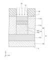
第1実施形態について説明する。第1実施形態は、炭化珪素を用いたいわゆる縦型のMOS型電界効果トランジスタ(field effect transistor:FET)に関し、このMOS型FETは炭化珪素半導体装置の一例である。図1は、第1実施形態に係る炭化珪素半導体装置の構成を示す断面図である。 (First embodiment)
A first embodiment will be described. The first embodiment relates to a so-called vertical MOS type field effect transistor (FET) using silicon carbide, and this MOS type FET is an example of a silicon carbide semiconductor device. FIG. 1 is a cross-sectional view showing the configuration of a silicon carbide semiconductor device according to a first embodiment.
図1に示されるように、第1実施形態に係る炭化珪素半導体装置100は、炭化珪素基板10と、ゲート絶縁膜81と、ゲート電極82と、層間絶縁膜83と、ソース電極60と、ドレイン電極70とを主に有している。
As shown in FIG. 1, a silicon carbide semiconductor device 100 according to the first embodiment includes a silicon carbide substrate 10, a gate insulating film 81, a gate electrode 82, an interlayer insulating film 83, a source electrode 60, and a drain. It mainly has an electrode 70.
炭化珪素基板10は、第1主面1と、第1主面1とは反対の第2主面2とを有する。第1主面1及び第2主面2はXY平面に平行であり、第1主面1は第2主面2からみて+Z方向にある。炭化珪素基板10は、炭化珪素単結晶基板50と、炭化珪素単結晶基板50上にある炭化珪素エピタキシャル層40とを含む。炭化珪素エピタキシャル層40は第1主面1を構成し、炭化珪素単結晶基板50は第2主面2を構成する。炭化珪素単結晶基板50及び炭化珪素エピタキシャル層40は、例えばポリタイプ4Hの六方晶炭化珪素から構成されている。炭化珪素単結晶基板50は、例えば窒素(N)等のn型不純物を含み、n型の導電型(第1導電型)を有する。
Silicon carbide substrate 10 has a first main surface 1 and a second main surface 2 opposite to first main surface 1 . The first main surface 1 and the second main surface 2 are parallel to the XY plane, and the first main surface 1 is in the +Z direction when viewed from the second main surface 2. Silicon carbide substrate 10 includes a silicon carbide single crystal substrate 50 and a silicon carbide epitaxial layer 40 on silicon carbide single crystal substrate 50. Silicon carbide epitaxial layer 40 constitutes first principal surface 1 , and silicon carbide single crystal substrate 50 constitutes second principal surface 2 . Silicon carbide single crystal substrate 50 and silicon carbide epitaxial layer 40 are made of, for example, hexagonal silicon carbide of polytype 4H. Silicon carbide single crystal substrate 50 contains an n-type impurity such as nitrogen (N), and has an n-type conductivity type (first conductivity type).
第1主面1は、{0001}面又は{0001}面がオフ方向に8°以下のオフ角だけ傾斜した面である。好ましくは、第1主面1は、(000-1)面又は(000-1)面がオフ方向に8°以下のオフ角だけ傾斜した面である。オフ方向は、例えば<11-20>方向であってもよいし、<1-100>方向であってもよい。オフ角は、例えば1°以上であってもよいし、2°以上であってもよい。オフ角は、6°以下であってもよいし、4°以下であってもよい。
The first principal surface 1 is a {0001} plane or a {0001} plane inclined in the off direction by an off angle of 8° or less. Preferably, the first principal surface 1 is a (000-1) plane or a plane in which the (000-1) plane is inclined in the off direction by an off angle of 8° or less. The off direction may be, for example, the <11-20> direction or the <1-100> direction. The off-angle may be, for example, 1° or more, or 2° or more. The off angle may be 6° or less, or 4° or less.
炭化珪素エピタキシャル層40は、ドリフト領域11と、ボディ領域12と、ソース領域13と、コンタクト領域18と、電界緩和領域16とを主に有する。
Silicon carbide epitaxial layer 40 mainly includes drift region 11 , body region 12 , source region 13 , contact region 18 , and electric field relaxation region 16 .
ドリフト領域11は、例えば窒素又はリン(P)等のn型不純物を含み、n型の導電型を有する。ドリフト領域11は、第1領域11Aと、第2領域11Bと、第3領域11Cと、第4領域11Dとを有する。
The drift region 11 contains an n-type impurity such as nitrogen or phosphorus (P), and has an n-type conductivity type. The drift region 11 has a first region 11A, a second region 11B, a third region 11C, and a fourth region 11D.
第4領域11Dは炭化珪素単結晶基板50の上に設けられている。第4領域11Dの下面と炭化珪素単結晶基板50の上面とが互いに接触する。第4領域11Dのn型不純物の実効濃度は、例えば1.0×1015cm-3以上5.0×1016cm-3以下である。
Fourth region 11D is provided on silicon carbide single crystal substrate 50. The lower surface of fourth region 11D and the upper surface of silicon carbide single crystal substrate 50 are in contact with each other. The effective concentration of n-type impurities in the fourth region 11D is, for example, 1.0×10 15 cm −3 or more and 5.0×10 16 cm −3 or less.
電界緩和領域16は、例えばアルミニウム(Al)等のp型不純物を含み、p型の導電型(第2導電型)を有する。電界緩和領域16は第4領域11Dの一部の上に設けられている。電界緩和領域16の下面と第4領域11Dの上面とが互いに接触する。電界緩和領域16のp型不純物の実効濃度は、例えば1.0×1016cm-3以上5.0×1018cm-3以下である。電界緩和領域16の下面が第4領域11Dの上面から離れ、これらの間に第3領域11Cの一部があってもよい。また、電界緩和領域16の下面と第3領域11Cの下面とが面一ではなく、電界緩和領域16の下面が第3領域11Cの下面よりも第2主面2に近くてもよい。つまり、電界緩和領域16が第3領域11Cよりも深く形成されていてもよい。
The electric field relaxation region 16 contains a p-type impurity such as aluminum (Al), and has a p-type conductivity type (second conductivity type). The electric field relaxation region 16 is provided on a part of the fourth region 11D. The lower surface of the electric field relaxation region 16 and the upper surface of the fourth region 11D are in contact with each other. The effective concentration of p-type impurities in the electric field relaxation region 16 is, for example, 1.0×10 16 cm −3 or more and 5.0×10 18 cm −3 or less. The lower surface of the electric field relaxation region 16 may be separated from the upper surface of the fourth region 11D, and a portion of the third region 11C may exist between them. Further, the lower surface of the electric field relaxation region 16 and the lower surface of the third region 11C may not be flush with each other, and the lower surface of the electric field relaxation region 16 may be closer to the second main surface 2 than the lower surface of the third region 11C. That is, the electric field relaxation region 16 may be formed deeper than the third region 11C.
第3領域11Cは第4領域11Dの一部の上に設けられている。第3領域11Cの下面と第4領域11Dの上面とが互いに接触する。第3領域11Cは電界緩和領域16に隣接する。第3領域11Cの側面と電界緩和領域16の側面とが互いに接触する。第3領域11Cのn型不純物の実効濃度は、例えば5.0×1015cm-3以上2.0×1018cm-3以下である。
The third region 11C is provided on a part of the fourth region 11D. The lower surface of the third region 11C and the upper surface of the fourth region 11D are in contact with each other. The third region 11C is adjacent to the electric field relaxation region 16. The side surface of the third region 11C and the side surface of the electric field relaxation region 16 are in contact with each other. The effective concentration of n-type impurities in the third region 11C is, for example, 5.0×10 15 cm −3 or more and 2.0×10 18 cm −3 or less.
第1領域11Aは電界緩和領域16の上に設けられている。第1領域11Aの下面と電界緩和領域16の上面とが互いに接触する。第1領域11Aのn型不純物の実効濃度は、例えば1.0×1016cm-3以上2.0×1018cm-3以下である。
The first region 11A is provided on the electric field relaxation region 16. The lower surface of the first region 11A and the upper surface of the electric field relaxation region 16 are in contact with each other. The effective concentration of n-type impurities in the first region 11A is, for example, 1.0×10 16 cm −3 or more and 2.0×10 18 cm −3 or less.
第2領域11Bは第3領域11Cの上に設けられている。第2領域11Bの下面と第3領域11Cの上面とが互いに接触する。第2領域11Bは第1領域11Aに隣接する。第2領域11Bの側面と第1領域11Aの側面とが互いに接触する。第2領域11Bのn型不純物の実効濃度は、例えば1.0×1016cm-3以上1.0×1018cm-3以下である。第1領域11A及び第2領域11Bが電流拡散領域とよばれることがある。
The second region 11B is provided on the third region 11C. The lower surface of the second region 11B and the upper surface of the third region 11C are in contact with each other. The second region 11B is adjacent to the first region 11A. The side surface of the second region 11B and the side surface of the first region 11A are in contact with each other. The effective concentration of n-type impurities in the second region 11B is, for example, 1.0×10 16 cm −3 or more and 1.0×10 18 cm −3 or less. The first region 11A and the second region 11B are sometimes called current diffusion regions.
例えば、第3領域11Cと第2領域11Bとの界面は、電界緩和領域16と第1領域11Aとの界面と面一である。第3領域11Cと第2領域11Bとの界面が、電界緩和領域16と第1領域11Aとの界面よりも第1主面1又は第2主面2に近くてもよい。第1領域11Aと第2領域11Bとの界面は、電界緩和領域16と第3領域11Cとの界面と面一であってもよく、第3領域11Cの上方にあってもよい。つまり、第1領域11Aの幅が電界緩和領域16の幅と等しくてもよく、電界緩和領域16の幅より広くてもよい。
For example, the interface between the third region 11C and the second region 11B is flush with the interface between the electric field relaxation region 16 and the first region 11A. The interface between the third region 11C and the second region 11B may be closer to the first main surface 1 or the second main surface 2 than the interface between the electric field relaxation region 16 and the first region 11A. The interface between the first region 11A and the second region 11B may be flush with the interface between the electric field relaxation region 16 and the third region 11C, or may be located above the third region 11C. That is, the width of the first region 11A may be equal to the width of the electric field relaxation region 16, or may be wider than the width of the electric field relaxation region 16.
このように、第1領域11Aは、電界緩和領域16と第1主面1との間に位置する。第2領域11Bは、第1主面1に平行な面内で第1領域11Aに隣接する。第3領域11Cは、第2領域11Bと第2主面2との間に位置し、第2領域11Bにつながり、第1主面1に平行な面内で電界緩和領域16に隣接する。第4領域11Dは、電界緩和領域16及び第3領域11Cと第2主面2との間に位置し、第3領域11Cにつながる。
In this way, the first region 11A is located between the electric field relaxation region 16 and the first main surface 1. The second region 11B is adjacent to the first region 11A in a plane parallel to the first main surface 1. The third region 11C is located between the second region 11B and the second main surface 2, is connected to the second region 11B, and is adjacent to the electric field relaxation region 16 in a plane parallel to the first main surface 1. The fourth region 11D is located between the electric field relaxation region 16 and the third region 11C and the second main surface 2, and is connected to the third region 11C.
ボディ領域12は、例えばアルミニウム等のp型不純物を含み、p型の導電型を有する。ボディ領域12はドリフト領域11の上に設けられている。ボディ領域12は第1領域11A及び第2領域11Bの上に設けられている。ボディ領域12のp型不純物の実効濃度は、例えば1.0×1017cm-3以上5.0×1018cm-3以下である。
Body region 12 contains, for example, a p-type impurity such as aluminum, and has p-type conductivity type. Body region 12 is provided above drift region 11 . The body region 12 is provided on the first region 11A and the second region 11B. The effective concentration of p-type impurities in the body region 12 is, for example, 1.0×10 17 cm −3 or more and 5.0×10 18 cm −3 or less.
ソース領域13は、例えば窒素又はリンなどのn型不純物を含み、n型の導電型を有する。ソース領域13はボディ領域12の上に設けられている。ソース領域13は、ボディ領域12によってドリフト領域11から隔てられている。ソース領域13は第1主面1を構成する。ソース領域13のn型不純物の実効濃度は、例えば5.0×1018cm-3以上2.0×1020cm-3以下である。
Source region 13 contains an n-type impurity such as nitrogen or phosphorus, and has n-type conductivity. Source region 13 is provided above body region 12 . Source region 13 is separated from drift region 11 by body region 12 . Source region 13 constitutes first main surface 1 . The effective concentration of n-type impurities in the source region 13 is, for example, 5.0×10 18 cm −3 or more and 2.0×10 20 cm −3 or less.
コンタクト領域18は、例えばアルミニウム等のp型不純物を含み、p型の導電型を有する。コンタクト領域18は、ソース領域13を貫通し、ボディ領域12に接する。コンタクト領域18は第1主面1を構成する。コンタクト領域18のp型不純物濃度の実効濃度は、例えば1.0×1018cm-3以上5.0×1020cm-3以下である。電界緩和領域16は電気的にコンタクト領域18に接続されている。なお、コンタクト領域18は、図1に示される断面とは異なる断面に現れる位置に形成されていてもよい。
Contact region 18 contains, for example, a p-type impurity such as aluminum, and has p-type conductivity type. Contact region 18 penetrates source region 13 and contacts body region 12 . Contact region 18 constitutes first main surface 1 . The effective p-type impurity concentration of the contact region 18 is, for example, 1.0×10 18 cm −3 or more and 5.0×10 20 cm −3 or less. Electric field relaxation region 16 is electrically connected to contact region 18 . Note that the contact region 18 may be formed at a position that appears in a cross section different from the cross section shown in FIG.
第1主面1に、側面3と底面4とにより規定されるゲートトレンチ5が設けられている。ゲートトレンチ5は、例えばY軸に沿って延びる。側面3は、ソース領域13と、ボディ領域12と、第1領域11Aの一部とを貫通し、第1領域11Aに至る。底面4は側面3と連なる。底面4は第1領域11Aに位置する。例えば、底面4は第1主面1及び第2主面2と平行である。底面4を含む平面に対する側面3の角度θ1は、例えば45°以上65°以下である。角度θ1は、例えば50°以上であってもよい。角度θ1は、例えば60°以下であってもよい。側面3は、好ましくは、{0-33-8}面を有する。{0-33-8}面は、優れた移動度が得られる結晶面である。
A gate trench 5 defined by a side surface 3 and a bottom surface 4 is provided on the first main surface 1 . Gate trench 5 extends, for example, along the Y axis. Side surface 3 penetrates source region 13, body region 12, and part of first region 11A, and reaches first region 11A. The bottom surface 4 is continuous with the side surface 3. The bottom surface 4 is located in the first region 11A. For example, the bottom surface 4 is parallel to the first main surface 1 and the second main surface 2. The angle θ1 of the side surface 3 with respect to the plane including the bottom surface 4 is, for example, 45° or more and 65° or less. The angle θ1 may be, for example, 50° or more. The angle θ1 may be, for example, 60° or less. The side surface 3 preferably has a {0-33-8} plane. The {0-33-8} plane is a crystal plane that provides excellent mobility.
ゲート絶縁膜81は、例えば酸化膜である。ゲート絶縁膜81は、例えば二酸化珪素を含む材料により構成されている。ゲート絶縁膜81は、側面3及び底面4に接する。ゲート絶縁膜81は、底面4において第1領域11Aと接する。ゲート絶縁膜81は、側面3においてソース領域13、ボディ領域12及び第1領域11Aと接する。ゲート絶縁膜81は、第1主面1においてソース領域13と接していてもよい。
The gate insulating film 81 is, for example, an oxide film. The gate insulating film 81 is made of a material containing silicon dioxide, for example. The gate insulating film 81 is in contact with the side surfaces 3 and the bottom surface 4 . The gate insulating film 81 is in contact with the first region 11A at the bottom surface 4. Gate insulating film 81 contacts source region 13, body region 12, and first region 11A on side surface 3. Gate insulating film 81 may be in contact with source region 13 on first main surface 1 .
ゲート電極82は、ゲート絶縁膜81の上に設けられている。ゲート電極82は、例えば導電性不純物を含むポリシリコン(ポリSi)から構成されている。ゲート電極82は、ゲートトレンチ5の内部に配置されている。ゲート電極82の一部は、第1主面1上に配置されていてもよい。
The gate electrode 82 is provided on the gate insulating film 81. The gate electrode 82 is made of, for example, polysilicon (polySi) containing conductive impurities. Gate electrode 82 is placed inside gate trench 5 . A portion of the gate electrode 82 may be placed on the first main surface 1.
層間絶縁膜83はゲート電極82を覆う。層間絶縁膜83はゲート電極82及びゲート絶縁膜81に接する。層間絶縁膜83は、例えば酸化膜である。層間絶縁膜83は、例えば二酸化珪素を含む材料から構成されている。層間絶縁膜83は、ゲート電極82とソース電極60とを互いに電気的に絶縁している。層間絶縁膜83の一部は、ゲートトレンチ5の内部に設けられていてもよい。
The interlayer insulating film 83 covers the gate electrode 82. Interlayer insulating film 83 is in contact with gate electrode 82 and gate insulating film 81 . The interlayer insulating film 83 is, for example, an oxide film. The interlayer insulating film 83 is made of a material containing silicon dioxide, for example. Interlayer insulating film 83 electrically insulates gate electrode 82 and source electrode 60 from each other. A portion of interlayer insulating film 83 may be provided inside gate trench 5 .
層間絶縁膜83の上面及び側面と、ゲート絶縁膜81の側面とを覆うバリアメタル膜84が設けられている。バリアメタル膜84は層間絶縁膜83及びゲート絶縁膜81と接している。バリアメタル膜84は、例えば窒化チタン(TiN)を含む材料から構成されている。
A barrier metal film 84 is provided to cover the top and side surfaces of the interlayer insulating film 83 and the side surfaces of the gate insulating film 81. Barrier metal film 84 is in contact with interlayer insulating film 83 and gate insulating film 81 . The barrier metal film 84 is made of a material containing, for example, titanium nitride (TiN).
層間絶縁膜83及びゲート絶縁膜81にコンタクトホール90が形成されている。コンタクトホール90を通じてソース領域13が層間絶縁膜83及びゲート絶縁膜81から露出している。
A contact hole 90 is formed in the interlayer insulating film 83 and the gate insulating film 81. Source region 13 is exposed from interlayer insulating film 83 and gate insulating film 81 through contact hole 90 .
ソース電極60は第1主面1に接する。ソース電極60は、コンタクトホール90内に設けられたコンタクト電極61と、ソース配線62とを有する。コンタクト電極61は、第1主面1において、ソース領域13及びコンタクト領域18に接している。コンタクト電極61は、例えばニッケルシリサイド(NiSi)を含む材料から構成されている。コンタクト電極61が、チタン(Ti)と、アルミニウムと、シリコンとを含む材料から構成されていてもよい。コンタクト電極61は、ソース領域13及びコンタクト領域18とオーミック接合している。ソース配線62は、層間絶縁膜83の上面及び側面と、コンタクト電極61の上面とを覆う。ソース配線62は、バリアメタル膜84及びコンタクト電極61と接している。ソース配線62は、例えばアルミニウムを含む材料から構成されている。ボディ領域12及び電界緩和領域16にはコンタクト領域18を介してソース電極60から電位が印加される。
The source electrode 60 is in contact with the first main surface 1. The source electrode 60 has a contact electrode 61 provided in the contact hole 90 and a source wiring 62. Contact electrode 61 is in contact with source region 13 and contact region 18 on first main surface 1 . The contact electrode 61 is made of a material containing, for example, nickel silicide (NiSi). The contact electrode 61 may be made of a material containing titanium (Ti), aluminum, and silicon. Contact electrode 61 is in ohmic contact with source region 13 and contact region 18 . The source wiring 62 covers the upper surface and side surfaces of the interlayer insulating film 83 and the upper surface of the contact electrode 61. The source wiring 62 is in contact with the barrier metal film 84 and the contact electrode 61. The source wiring 62 is made of a material containing aluminum, for example. A potential is applied to body region 12 and electric field relaxation region 16 from source electrode 60 via contact region 18 .
ドレイン電極70は第2主面2に接する。ドレイン電極70は、第2主面2において炭化珪素単結晶基板50と接している。ドレイン電極70は、ドリフト領域11と電気的に接続されている。ドレイン電極70は、例えばニッケルシリサイドを含む材料から構成されている。ドレイン電極70がチタンと、アルミニウムと、シリコンとを含む材料から構成されていてもよい。ドレイン電極70は、炭化珪素単結晶基板50とオーミック接合している。
The drain electrode 70 is in contact with the second main surface 2. Drain electrode 70 is in contact with silicon carbide single crystal substrate 50 at second main surface 2 . Drain electrode 70 is electrically connected to drift region 11 . The drain electrode 70 is made of a material containing, for example, nickel silicide. The drain electrode 70 may be made of a material containing titanium, aluminum, and silicon. Drain electrode 70 is in ohmic contact with silicon carbide single crystal substrate 50 .
炭化珪素単結晶基板50と第4領域11Dとの間に、例えば窒素等のn型不純物を含み、n型の導電型を有するバッファ層が設けられていてもよい。バッファ層のn型不純物の実効濃度は、第4領域11Dのn型不純物の実効濃度よりも高くてもよい。
A buffer layer containing an n-type impurity such as nitrogen and having n-type conductivity may be provided between silicon carbide single crystal substrate 50 and fourth region 11D. The effective concentration of n-type impurities in the buffer layer may be higher than the effective concentration of n-type impurities in the fourth region 11D.
p型の領域におけるp型不純物の実効濃度とは、当該領域におけるp型不純物の濃度からn型不純物の濃度を減じて得られる値である。n型の領域におけるn型不純物の実効濃度とは、当該領域におけるn型不純物の濃度からp型不純物の濃度を減じて得られる値である。p型不純物の実効濃度及びn型不純物の実効濃度は、例えば走査型静電容量顕微鏡(Scanning Capacitance Microscope:SCM)法又は二次イオン質量分析(Secondary Ion Mass Spectrometry:SIMS)法等により測定可能である。p型の領域とn型の領域との境界面(つまりpn接合界面)の位置は、例えばSCM法又はSIMS法などにより特定できる。
The effective concentration of p-type impurities in a p-type region is a value obtained by subtracting the concentration of n-type impurities from the concentration of p-type impurities in the region. The effective concentration of n-type impurities in an n-type region is a value obtained by subtracting the concentration of p-type impurities from the concentration of n-type impurities in the region. The effective concentration of p-type impurities and the effective concentration of n-type impurities can be measured, for example, by a scanning capacitance microscope (SCM) method or a secondary ion mass spectrometry (SIMS) method. be. The position of the interface between the p-type region and the n-type region (that is, the pn junction interface) can be specified by, for example, the SCM method or the SIMS method.
次に、第1実施形態における各領域の間の実効濃度の関係について説明する。図2は、不純物の実効濃度の分布の一例を示す図である。図2には、図1中の二点鎖線Lに沿った不純物の実効濃度の絶対値の分布を示す。図2の横軸は第1主面1を基準とした深さを示し、縦軸は不純物の実効濃度の絶対値を示す。
Next, the relationship in effective concentration between each region in the first embodiment will be explained. FIG. 2 is a diagram showing an example of the distribution of effective concentration of impurities. FIG. 2 shows the distribution of the absolute value of the effective concentration of impurities along the two-dot chain line L in FIG. The horizontal axis in FIG. 2 indicates the depth with respect to the first main surface 1, and the vertical axis indicates the absolute value of the effective concentration of impurities.
本実施形態では、第1領域11Aにおけるn型不純物の実効濃度の第1最大値が、第2領域11Bにおけるn型不純物の実効濃度の第2最大値よりも高い。第3領域11Cにおけるn型不純物の実効濃度の第3最大値が、第2最大値以下である。第4領域11Dにおけるn型不純物の実効濃度の第4最大値が、第3最大値以下である。
In this embodiment, the first maximum value of the effective concentration of n-type impurities in the first region 11A is higher than the second maximum value of the effective concentration of n-type impurities in the second region 11B. The third maximum value of the effective concentration of n-type impurities in the third region 11C is less than or equal to the second maximum value. The fourth maximum value of the effective concentration of n-type impurities in the fourth region 11D is equal to or less than the third maximum value.
図2に示すように、ソース領域13におけるn型不純物の実効濃度の最大値が、ボディ領域12におけるp型不純物の実効濃度の最大値より高くてよい。ボディ領域12におけるp型不純物の実効濃度の最大値が、第1領域11Aにおけるn型不純物の実効濃度の第1最大値より高くてよい。第1領域11Aにおけるn型不純物の実効濃度の第1最大値が、電界緩和領域16におけるp型不純物の実効濃度の第5最大値より高くてよい。
As shown in FIG. 2, the maximum effective concentration of n-type impurities in source region 13 may be higher than the maximum effective concentration of p-type impurities in body region 12. The maximum value of the effective concentration of p-type impurities in body region 12 may be higher than the first maximum value of the effective concentration of n-type impurities in first region 11A. The first maximum value of the effective concentration of n-type impurities in the first region 11A may be higher than the fifth maximum value of the effective concentration of p-type impurities in the electric field relaxation region 16.
次に、第1実施形態に係る炭化珪素半導体装置100の製造方法について説明する。図3から図11は、第1実施形態に係る炭化珪素半導体装置の製造方法を示す断面図である。
Next, a method for manufacturing silicon carbide semiconductor device 100 according to the first embodiment will be described. 3 to 11 are cross-sectional views showing a method of manufacturing a silicon carbide semiconductor device according to the first embodiment.
まず、図3に示されるように、炭化珪素単結晶基板50を準備する。次に、炭化珪素単結晶基板50の上に炭化珪素エピタキシャル層40を形成する。炭化珪素エピタキシャル層40は、第4領域11Dと、後に第3領域11C等が形成されるn型領域111Cとを含む。例えば、炭化珪素単結晶基板50は、窒素等のn型不純物を含み、n型の導電型を有する。例えば、炭化珪素エピタキシャル層40は窒素等のn型不純物を添加したエピタキシャル成長により形成できる。このようにして、第1主面1と、第2主面2とを有する炭化珪素基板10が得られる。
First, as shown in FIG. 3, a silicon carbide single crystal substrate 50 is prepared. Next, silicon carbide epitaxial layer 40 is formed on silicon carbide single crystal substrate 50 . Silicon carbide epitaxial layer 40 includes a fourth region 11D and an n-type region 111C in which a third region 11C and the like will be formed later. For example, silicon carbide single crystal substrate 50 contains n-type impurities such as nitrogen and has n-type conductivity type. For example, silicon carbide epitaxial layer 40 can be formed by epitaxial growth doped with n-type impurities such as nitrogen. In this way, silicon carbide substrate 10 having first main surface 1 and second main surface 2 is obtained.
次に、図4に示されるように、炭化珪素エピタキシャル層40の上にレジストマスク30を形成する。レジストマスク30には、n型領域111Cの電界緩和領域16を形成する領域を露出する開口31が形成されている。
Next, as shown in FIG. 4, a resist mask 30 is formed on the silicon carbide epitaxial layer 40. An opening 31 is formed in the resist mask 30 to expose a region where the electric field relaxation region 16 of the n-type region 111C is to be formed.
次に、図5に示されるように、開口31を通じたp型不純物21のイオン注入を行うことにより、n型領域111C内にp型領域116を形成する。p型領域116は電界緩和領域16となる領域であるが、電界緩和領域16よりも浅い領域まで形成する。p型不純物21のイオン注入では、例えばチャネリング注入を行う。つまり、{0001}面に垂直にイオン注入を行う。
Next, as shown in FIG. 5, p-type impurity 21 is ion-implanted through opening 31 to form p-type region 116 in n-type region 111C. The p-type region 116 is a region that becomes the electric field relaxation region 16, and is formed to a shallower region than the electric field relaxation region 16. In the ion implantation of the p-type impurity 21, channeling implantation is performed, for example. That is, ion implantation is performed perpendicularly to the {0001} plane.
次に、図6に示されるように、開口31を通じたn型不純物22のイオン注入を行うことにより、n型領域111C内にn型領域111Aを形成する。n型領域111Aは第1領域11Aとなる領域であるが、第1領域11Aよりも浅い領域まで形成する。例えば、n型領域111Aは第1主面1を構成する。また、n型領域111Aはp型領域116の一部と重なるように形成する。n型領域111Aの形成に伴って、p型領域116から電界緩和領域16が形成される。n型不純物22のイオン注入では、Z軸に沿って第1主面1に垂直にイオン注入を行う。
Next, as shown in FIG. 6, an n-type impurity 22 is ion-implanted through the opening 31 to form an n-type region 111A within the n-type region 111C. The n-type region 111A is a region that becomes the first region 11A, but is formed to a shallower region than the first region 11A. For example, the n-type region 111A constitutes the first main surface 1. Further, the n-type region 111A is formed so as to partially overlap the p-type region 116. Along with the formation of n-type region 111A, electric field relaxation region 16 is formed from p-type region 116. In the ion implantation of the n-type impurity 22, ions are implanted perpendicularly to the first main surface 1 along the Z axis.
次に、図7に示されるように、レジストマスク30を除去し、第1主面1の全体へのp型不純物23のイオン注入を行うことにより、n型領域111C及び111A内にp型領域112を形成する。p型領域112はボディ領域12となる領域であるが、ボディ領域12よりも浅い領域まで形成する。例えば、p型領域112は第1主面1を構成する。p型不純物23のイオン注入では、Z軸に沿って第1主面1に垂直にイオン注入を行う。
Next, as shown in FIG. 7, the resist mask 30 is removed and p-type impurity 23 is ion-implanted into the entire first main surface 1, thereby forming p-type regions in the n-type regions 111C and 111A. 112 is formed. Although the p-type region 112 is a region that will become the body region 12, it is formed to a shallower region than the body region 12. For example, p-type region 112 constitutes first main surface 1 . In the ion implantation of the p-type impurity 23, ions are implanted perpendicularly to the first main surface 1 along the Z axis.
次に、図8に示されるように、第1主面1の全体へのn型不純物24のイオン注入を行うことにより、p型領域112内にn型領域113を形成し、n型領域111A内に第1領域11Aを形成し、n型領域111C内に第2領域11Bを形成する。第2領域11Bの形成に伴って、n型領域111Cから第3領域11Cが形成される。n型不純物24のイオン注入では、Z軸に沿って第1主面1に垂直にイオン注入を行う。
Next, as shown in FIG. 8, an n-type impurity 24 is ion-implanted into the entire first main surface 1 to form an n-type region 113 in the p-type region 112, and an n-type region 111A A first region 11A is formed within the n-type region 111C, and a second region 11B is formed within the n-type region 111C. Along with the formation of the second region 11B, a third region 11C is formed from the n-type region 111C. In the ion implantation of the n-type impurity 24, the ion implantation is performed perpendicularly to the first main surface 1 along the Z axis.
次に、図9に示されるように、レジストマスク(図示せず)を用いた第1主面1の一部へのp型不純物のイオン注入を行うことにより、n型領域113内にコンタクト領域18を形成する。コンタクト領域18の形成に伴って、n型領域113からソース領域13が形成される。p型不純物のイオン注入では、Z軸に沿って第1主面1に垂直にイオン注入を行う。
Next, as shown in FIG. 9, a contact region is formed in the n-type region 113 by implanting p-type impurity ions into a part of the first main surface 1 using a resist mask (not shown). form 18. Along with the formation of contact region 18, source region 13 is formed from n-type region 113. In the ion implantation of p-type impurities, ions are implanted perpendicularly to the first main surface 1 along the Z axis.
次に、図10に示されるように、側面3及び底面4を備えたゲートトレンチ5を形成する。ゲートトレンチ5は、例えばマスクを用いた、反応性イオンエッチング(reactive ion etching:RIE)及び熱エッチング等により形成できる。
Next, as shown in FIG. 10, a gate trench 5 having side surfaces 3 and a bottom surface 4 is formed. The gate trench 5 can be formed by, for example, reactive ion etching (RIE), thermal etching, etc. using a mask.
次に、図11に示されるように、ゲート絶縁膜81、ゲート電極82及び層間絶縁膜83を形成する。次に、ゲート絶縁膜81及び層間絶縁膜83にコンタクトホール90を形成し、バリアメタル膜84を形成する。次に、コンタクト電極61及びソース配線62を備えたソース電極60を形成する。また、ドレイン電極70を形成する。
Next, as shown in FIG. 11, a gate insulating film 81, a gate electrode 82, and an interlayer insulating film 83 are formed. Next, a contact hole 90 is formed in the gate insulating film 81 and the interlayer insulating film 83, and a barrier metal film 84 is formed. Next, a source electrode 60 including a contact electrode 61 and a source wiring 62 is formed. Additionally, a drain electrode 70 is formed.
このようにして、第1実施形態に係る炭化珪素半導体装置100を製造できる。
In this way, silicon carbide semiconductor device 100 according to the first embodiment can be manufactured.
第1実施形態に係る炭化珪素半導体装置100では、第1領域11Aにおけるn型不純物の実効濃度の第1最大値が、第2領域11Bにおけるn型不純物の実効濃度の第2最大値よりも高い。このため、オン抵抗を低減しながら、ボディ領域12の下方での過度な電界集中を抑制して高い耐圧を得られる。また、第2最大値が第1最大値よりも小さいため、ソース電極60とドレイン電極70との間の容量を低く抑えてスイッチング損失を低減できる。
In silicon carbide semiconductor device 100 according to the first embodiment, the first maximum value of the effective concentration of n-type impurities in first region 11A is higher than the second maximum value of the effective concentration of n-type impurities in second region 11B. . Therefore, while reducing the on-resistance, it is possible to suppress excessive electric field concentration below the body region 12 and obtain a high breakdown voltage. Further, since the second maximum value is smaller than the first maximum value, the capacitance between the source electrode 60 and the drain electrode 70 can be kept low, and switching loss can be reduced.
また、第3領域11Cにおけるn型不純物の実効濃度の第3最大値が、第2最大値以下である。このため、第2領域11Bにおける電気抵抗の上昇を抑制できる。好ましくは、第3最大値は第4最大値よりも高い。
Further, the third maximum value of the effective concentration of n-type impurities in the third region 11C is equal to or less than the second maximum value. Therefore, an increase in electrical resistance in the second region 11B can be suppressed. Preferably, the third maximum value is higher than the fourth maximum value.
また、第4領域11Dにおけるn型不純物の実効濃度の第4最大値が、第3最大値以下である。このため、第3領域11Cにおける電気抵抗の上昇を抑制できる。例えば、電界緩和領域16と第3領域11Cとが交互に並び、複数のセルが配置された場合でも、隣り合う電界緩和領域16の間の第3領域11Cにおける電気抵抗を低く抑制できる。好ましくは、第3最大値は第2最大値よりも低い。
Furthermore, the fourth maximum value of the effective concentration of n-type impurities in the fourth region 11D is equal to or less than the third maximum value. Therefore, an increase in electrical resistance in the third region 11C can be suppressed. For example, even if the electric field relaxation regions 16 and the third regions 11C are arranged alternately and a plurality of cells are arranged, the electrical resistance in the third region 11C between the adjacent electric field relaxation regions 16 can be suppressed to a low level. Preferably, the third maximum value is lower than the second maximum value.
電界緩和領域16は、第1領域11Aと接する第1面41と、第1面41とは反対の第2面42と、を有する。好ましくは、図2に示すように、電界緩和領域16におけるp型不純物の実効濃度は、第1面41から第2面42に向かって0.3μm離れた第1仮想面51から第2面42にかけて漸減している。この場合、ゲートトレンチ5の底部におけるゲート絶縁膜81への電界集中を緩和しやすい。
The electric field relaxation region 16 has a first surface 41 in contact with the first region 11A, and a second surface 42 opposite to the first surface 41. Preferably, as shown in FIG. 2, the effective concentration of p-type impurities in the electric field relaxation region 16 is from the first virtual surface 51 to the second surface 42, which is 0.3 μm apart from the first surface 41 toward the second surface 42. It gradually decreases over time. In this case, electric field concentration on the gate insulating film 81 at the bottom of the gate trench 5 can be easily alleviated.
第1最大値は、電界緩和領域16におけるp型不純物の実効濃度の第5最大値の、好ましくは50%以上である。この場合、オン抵抗を低減しやすい。第1最大値は第5最大値の、より好ましくは60%以上であり、更に好ましくは70%以上である。なお、ボディ領域12のチャネルとして機能する部分におけるパンチスルーを抑制するために、第1最大値はボディ領域12におけるp型不純物の実効濃度の最大値より低いことが好ましい。
The first maximum value is preferably 50% or more of the fifth maximum value of the effective concentration of p-type impurities in the electric field relaxation region 16. In this case, it is easy to reduce the on-resistance. The first maximum value is preferably 60% or more, and even more preferably 70% or more, of the fifth maximum value. Note that, in order to suppress punch-through in the portion of the body region 12 that functions as a channel, the first maximum value is preferably lower than the maximum value of the effective concentration of p-type impurities in the body region 12.
第2最大値は、電界緩和領域16におけるp型不純物の実効濃度の第5最大値の、好ましくは20%以上である。この場合、アバランシェ降伏時に、第2領域11B上においてボディ領域12内の電界が電界緩和領域16内の電界よりも高くなりやすい。電界集中が生じる箇所が分散され、より高い耐圧が得られる。第2最大値は第5最大値の、より好ましくは30%以上であり、更に好ましくは40%以上である。
The second maximum value is preferably 20% or more of the fifth maximum value of the effective concentration of p-type impurities in the electric field relaxation region 16. In this case, at the time of avalanche breakdown, the electric field in the body region 12 tends to be higher than the electric field in the electric field relaxation region 16 on the second region 11B. The locations where electric field concentration occurs are dispersed, resulting in higher breakdown voltage. The second maximum value is preferably 30% or more, and even more preferably 40% or more, of the fifth maximum value.
第3領域11Cは、第1面41と面一の第3面43を有する。第3面43は第2領域11Bに接する。第3領域11Cは、更に第5領域11Eを有する。第5領域11Eは、第3面43と、第3面43から第2主面2に向かって1μm離れた第2仮想面52との間の領域である。電界緩和領域16の厚さは1μm以上であり、第3面43から第2主面2に向かって第1距離だけ離れた位置での第5領域11Eにおけるn型不純物の実効濃度は、第1面41から第2主面2に向かって第1距離だけ離れた位置での電界緩和領域16におけるp型不純物の実効濃度の、好ましくは10%以上であり、より好ましくは20%以上であり、更に好ましくは30%以上である。このような関係が成り立つ場合、電界緩和領域16内の空乏化が促進されやすい。また、第2領域11B上においてボディ領域12内に電界集中が生じやすくなる。このため、より高い耐圧が得られる。電界緩和領域16の厚さは、好ましくは1μm以上であり、より好ましくは1.5μm以上であり、更に好ましくは2μm以上である。
The third region 11C has a third surface 43 that is flush with the first surface 41. The third surface 43 contacts the second region 11B. The third region 11C further includes a fifth region 11E. The fifth region 11E is a region between the third surface 43 and the second virtual surface 52 that is 1 μm away from the third surface 43 toward the second main surface 2. The thickness of the electric field relaxation region 16 is 1 μm or more, and the effective concentration of n-type impurities in the fifth region 11E at a position away from the third surface 43 by the first distance toward the second main surface 2 is the first It is preferably 10% or more, more preferably 20% or more of the effective concentration of the p-type impurity in the electric field relaxation region 16 at a position separated by the first distance from the surface 41 toward the second main surface 2, More preferably, it is 30% or more. When such a relationship holds true, depletion within the electric field relaxation region 16 is likely to be promoted. Further, electric field concentration tends to occur in the body region 12 on the second region 11B. Therefore, higher breakdown voltage can be obtained. The thickness of the electric field relaxation region 16 is preferably 1 μm or more, more preferably 1.5 μm or more, and still more preferably 2 μm or more.
本実施形態では、ゲートトレンチ5の底面4が第1領域11Aにより構成されることで、オン抵抗を低減しやすい。また、第1領域11Aの幅が電界緩和領域16の幅よりも広い場合には、よりオン抵抗を低減しやすい。
In this embodiment, since the bottom surface 4 of the gate trench 5 is constituted by the first region 11A, it is easy to reduce the on-resistance. Further, when the width of the first region 11A is wider than the width of the electric field relaxation region 16, it is easier to reduce the on-resistance.
(第2実施形態)
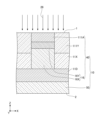
第2実施形態について説明する。第2実施形態は、主として、電界緩和領域16の構成の点で第1実施形態と相違する。図12は、第2実施形態に係る炭化珪素半導体装置を示す断面図である。 (Second embodiment)
A second embodiment will be described. The second embodiment differs from the first embodiment mainly in the configuration of the electricfield relaxation region 16. FIG. 12 is a cross-sectional view showing a silicon carbide semiconductor device according to a second embodiment.
第2実施形態について説明する。第2実施形態は、主として、電界緩和領域16の構成の点で第1実施形態と相違する。図12は、第2実施形態に係る炭化珪素半導体装置を示す断面図である。 (Second embodiment)
A second embodiment will be described. The second embodiment differs from the first embodiment mainly in the configuration of the electric
図12に示されるように、第2実施形態に係る炭化珪素半導体装置200では、電界緩和領域16が第6領域16Xと、第7領域16Yとを有する。第6領域16Xは、第4領域11Dの一部の上に設けられている。第6領域16Xの下面と第4領域11Dの上面とが互いに接触する。第7領域16Yは第6領域16Xの上に設けられている。第7領域16Yの下面と第6領域16Xの上面とが互いに接触する。また、第7領域16Yの上面と第1領域11Aの下面とが互いに接触する。第7領域16Yのp型不純物の実効濃度は、第6領域16Xのp型不純物の実効濃度よりも高い。第6領域16Xのp型不純物の実効濃度は、例えば1.0×1016cm-3以上4.0×1018cm-3以下である。第7領域16Yのp型不純物の実効濃度は、例えば1.0×1017cm-3以上5.0×1018cm-3以下である。
As shown in FIG. 12, in silicon carbide semiconductor device 200 according to the second embodiment, electric field relaxation region 16 includes sixth region 16X and seventh region 16Y. The sixth region 16X is provided on a part of the fourth region 11D. The lower surface of the sixth region 16X and the upper surface of the fourth region 11D are in contact with each other. The seventh region 16Y is provided on the sixth region 16X. The lower surface of the seventh region 16Y and the upper surface of the sixth region 16X are in contact with each other. Further, the upper surface of the seventh region 16Y and the lower surface of the first region 11A are in contact with each other. The effective concentration of p-type impurities in the seventh region 16Y is higher than the effective concentration of p-type impurities in the sixth region 16X. The effective concentration of p-type impurities in the sixth region 16X is, for example, 1.0×10 16 cm −3 or more and 4.0×10 18 cm −3 or less. The effective concentration of p-type impurities in the seventh region 16Y is, for example, 1.0×10 17 cm −3 or more and 5.0×10 18 cm −3 or less.
他の構成は第1実施形態と同一である。
The other configurations are the same as the first embodiment.
次に、第2実施形態に係る炭化珪素半導体装置200の製造方法について説明する。図13は、第2実施形態に係る炭化珪素半導体装置の製造方法を示す断面図である。
Next, a method for manufacturing silicon carbide semiconductor device 200 according to the second embodiment will be described. FIG. 13 is a cross-sectional view showing a method for manufacturing a silicon carbide semiconductor device according to a second embodiment.
まず、第1実施形態に倣って、n型不純物22のイオン注入までの処理を行う(図6参照)。本実施形態では、n型領域111Aが形成された時点では、電界緩和領域16は形成されない。次に、図13に示されるように、開口31を通じたp型不純物25のイオン注入を行うことにより、p型領域116内に第7領域16Yを形成する。第7領域16Yの形成に伴って、p型領域116から第6領域16Xが形成される。この結果、第6領域16X及び第7領域16Yを有する電界緩和領域16が形成される。p型不純物25のイオン注入では、Z軸に沿って第1主面1に垂直にイオン注入を行う。
First, following the first embodiment, processing up to ion implantation of the n-type impurity 22 is performed (see FIG. 6). In this embodiment, the electric field relaxation region 16 is not formed at the time when the n-type region 111A is formed. Next, as shown in FIG. 13, the p-type impurity 25 is ion-implanted through the opening 31 to form a seventh region 16Y in the p-type region 116. Along with the formation of the seventh region 16Y, a sixth region 16X is formed from the p-type region 116. As a result, an electric field relaxation region 16 having a sixth region 16X and a seventh region 16Y is formed. In the ion implantation of the p-type impurity 25, the ion implantation is performed perpendicularly to the first main surface 1 along the Z axis.
その後、第1実施形態に倣って、レジストマスク30の除去以降の処理を行う。このようにして、第2実施形態に係る炭化珪素半導体装置200を製造できる。
Then, following the first embodiment, the process after removing the resist mask 30 is performed. In this way, silicon carbide semiconductor device 200 according to the second embodiment can be manufactured.
第2実施形態によっても第1実施形態と同一の効果が得られる。
The second embodiment also provides the same effects as the first embodiment.
(第3実施形態)
第3実施形態について説明する。第3実施形態は、主として、第3領域11Cの構成の点で第2実施形態と相違する。図14は、第3実施形態に係る炭化珪素半導体装置を示す断面図である。 (Third embodiment)
A third embodiment will be described. The third embodiment differs from the second embodiment mainly in the configuration of thethird region 11C. FIG. 14 is a cross-sectional view showing a silicon carbide semiconductor device according to a third embodiment.
第3実施形態について説明する。第3実施形態は、主として、第3領域11Cの構成の点で第2実施形態と相違する。図14は、第3実施形態に係る炭化珪素半導体装置を示す断面図である。 (Third embodiment)
A third embodiment will be described. The third embodiment differs from the second embodiment mainly in the configuration of the
図14に示されるように、第3実施形態に係る炭化珪素半導体装置300では、第3領域11Cが第8領域11Xと、第9領域11Yとを有する。第8領域11Xは、第4領域11Dの一部の上に設けられている。第8領域11Xの下面と第4領域11Dの上面とが互いに接触する。第9領域11Yは第8領域11Xの上に設けられている。第9領域11Yの下面と第8領域11Xの上面とが互いに接触する。また、第9領域11Yの上面と第2領域11Bの下面とが互いに接触する。第9領域11Yのn型不純物の実効濃度は、第8領域11Xのp型不純物の実効濃度よりも高い。第8領域11Xのn型不純物の実効濃度は、例えば5.0×1015cm-3以上5.0×1017cm-3以下である。第9領域11Yのn型不純物の実効濃度は、例えば1.0×1016cm-3以上1.0×1018cm-3以下である。
As shown in FIG. 14, in silicon carbide semiconductor device 300 according to the third embodiment, third region 11C includes eighth region 11X and ninth region 11Y. The eighth region 11X is provided on a part of the fourth region 11D. The lower surface of the eighth region 11X and the upper surface of the fourth region 11D are in contact with each other. The ninth region 11Y is provided on the eighth region 11X. The lower surface of the ninth region 11Y and the upper surface of the eighth region 11X are in contact with each other. Further, the upper surface of the ninth region 11Y and the lower surface of the second region 11B are in contact with each other. The effective concentration of n-type impurities in the ninth region 11Y is higher than the effective concentration of p-type impurities in the eighth region 11X. The effective concentration of n-type impurities in the eighth region 11X is, for example, 5.0×10 15 cm −3 or more and 5.0×10 17 cm −3 or less. The effective concentration of n-type impurities in the ninth region 11Y is, for example, 1.0×10 16 cm −3 or more and 1.0×10 18 cm −3 or less.
他の構成は第2実施形態と同一である。
The other configurations are the same as the second embodiment.
なお、第8領域11Xと第9領域11Yとの界面は、第2仮想面52(図1参照)と一致していてもよく、第2仮想面52より第1主面1に近くてもよく、第2仮想面52より第2主面2に近くてもよい。上記のように、第2仮想面52は、第2領域11Bに接する第3面43から第2主面2に向かって1μm離れた面である。
Note that the interface between the eighth region 11X and the ninth region 11Y may coincide with the second virtual surface 52 (see FIG. 1), and may be closer to the first principal surface 1 than the second virtual surface 52. , may be closer to the second principal surface 2 than the second virtual surface 52. As described above, the second virtual surface 52 is a surface that is 1 μm away from the third surface 43 in contact with the second region 11B toward the second main surface 2.
次に、第3実施形態に係る炭化珪素半導体装置300の製造方法について説明する。図15及びは、第3実施形態に係る炭化珪素半導体装置の製造方法を示す断面図である。
Next, a method for manufacturing silicon carbide semiconductor device 300 according to the third embodiment will be described. FIG. 15 and FIG. 15 are cross-sectional views showing a method for manufacturing a silicon carbide semiconductor device according to a third embodiment.
まず、図15に示されるように、第2実施形態に倣って、レジストマスク30の除去までの処理を行う。次に、図16に示されるように、第1主面1の全体へのn型不純物26のイオン注入を行うことにより、n型領域111C内にn型領域111Yを形成する。n型領域111Yは第9領域11Yとなる領域であるが、第9領域11Yよりも浅い領域まで形成する。例えば、n型領域111Yは第1主面1を構成する。n型領域111Yの形成に伴って、n型領域111Cから第8領域11Xが形成される。n型不純物26のイオン注入では、例えばチャネリング注入を行う。つまり、{0001}面に垂直にイオン注入を行う。
First, as shown in FIG. 15, processing up to the removal of the resist mask 30 is performed in accordance with the second embodiment. Next, as shown in FIG. 16, an n-type impurity 26 is ion-implanted into the entire first main surface 1 to form an n-type region 111Y in the n-type region 111C. The n-type region 111Y is a region that will become the ninth region 11Y, and is formed to a shallower region than the ninth region 11Y. For example, the n-type region 111Y constitutes the first main surface 1. With the formation of n-type region 111Y, eighth region 11X is formed from n-type region 111C. In the ion implantation of the n-type impurity 26, channeling implantation is performed, for example. That is, ion implantation is performed perpendicularly to the {0001} plane.
その後、第1実施形態に倣って、p型領域112の形成以降の処理を行う。第1主面1の全体へのn型不純物24のイオン注入により第2領域11Bが形成され(図8参照)、第2領域11Bの形成に伴って、n型領域111Xから第9領域11Yが形成される(図14参照)。この結果、第8領域11X及び第9領域11Yを有する第3領域11Cが形成される。このようにして、第3実施形態に係る炭化珪素半導体装置300を製造できる。
Thereafter, processes after forming the p-type region 112 are performed in accordance with the first embodiment. The second region 11B is formed by ion implantation of the n-type impurity 24 into the entire first main surface 1 (see FIG. 8), and with the formation of the second region 11B, the ninth region 11Y is expanded from the n-type region 111X. (See FIG. 14). As a result, a third region 11C having an eighth region 11X and a ninth region 11Y is formed. In this way, silicon carbide semiconductor device 300 according to the third embodiment can be manufactured.
第3実施形態によっても第1実施形態及び第2実施形態と同一の効果が得られる。
The third embodiment also provides the same effects as the first and second embodiments.
なお、イオン注入に用いるマスクとして、レジストマスクに代えて、ポリシリコン又は酸化シリコン等のハードマスクを用いてもよい。
Note that as a mask used for ion implantation, a hard mask such as polysilicon or silicon oxide may be used instead of a resist mask.
以上、実施形態について詳述したが、特定の実施形態に限定されるものではなく、請求の範囲に記載された範囲内において、種々の変形及び変更が可能である。
Although the embodiments have been described in detail above, they are not limited to specific embodiments, and various modifications and changes are possible within the scope of the claims.
1 第1主面
2 第2主面
3 側面
4 底面
5 ゲートトレンチ
10 炭化珪素基板
11 ドリフト領域
11A 第1領域
11B 第2領域
11C 第3領域
11D 第4領域
11E 第5領域
11X 第8領域
11Y 第9領域
12 ボディ領域
13 ソース領域
16 電界緩和領域
16X 第6領域
16Y 第7領域
21、23、25 p型不純物
22、24、26 n型不純物
30 レジストマスク
31 開口
40 炭化珪素エピタキシャル層
41 第1面
42 第2面
43 第3面
50 炭化珪素単結晶基板
51 第1仮想面
52 第2仮想面
60 ソース電極
61 コンタクト電極
62 ソース配線
70 ドレイン電極
81 ゲート絶縁膜
82 ゲート電極
83 層間絶縁膜
84 バリアメタル膜
90 コンタクトホール
100、200、300 炭化珪素半導体装置
111A、111C、111X、111Y n型領域
112、116 p型領域
113 n型領域 1 Firstmain surface 2 Second main surface 3 Side surface 4 Bottom surface 5 Gate trench 10 Silicon carbide substrate 11 Drift region 11A First region 11B Second region 11C Third region 11D Fourth region 11E Fifth region 11X Eighth region 11Y 9 region 12 Body region 13 Source region 16 Electric field relaxation region 16X Sixth region 16Y Seventh region 21, 23, 25 P- type impurity 22, 24, 26 N-type impurity 30 Resist mask 31 Opening 40 Silicon carbide epitaxial layer 41 First surface 42 Second surface 43 Third surface 50 Silicon carbide single crystal substrate 51 First virtual surface 52 Second virtual surface 60 Source electrode 61 Contact electrode 62 Source wiring 70 Drain electrode 81 Gate insulating film 82 Gate electrode 83 Interlayer insulating film 84 Barrier metal Film 90 Contact holes 100, 200, 300 Silicon carbide semiconductor devices 111A, 111C, 111X, 111Y N-type regions 112, 116 P-type region 113 N-type region
2 第2主面
3 側面
4 底面
5 ゲートトレンチ
10 炭化珪素基板
11 ドリフト領域
11A 第1領域
11B 第2領域
11C 第3領域
11D 第4領域
11E 第5領域
11X 第8領域
11Y 第9領域
12 ボディ領域
13 ソース領域
16 電界緩和領域
16X 第6領域
16Y 第7領域
21、23、25 p型不純物
22、24、26 n型不純物
30 レジストマスク
31 開口
40 炭化珪素エピタキシャル層
41 第1面
42 第2面
43 第3面
50 炭化珪素単結晶基板
51 第1仮想面
52 第2仮想面
60 ソース電極
61 コンタクト電極
62 ソース配線
70 ドレイン電極
81 ゲート絶縁膜
82 ゲート電極
83 層間絶縁膜
84 バリアメタル膜
90 コンタクトホール
100、200、300 炭化珪素半導体装置
111A、111C、111X、111Y n型領域
112、116 p型領域
113 n型領域 1 First
Claims (9)
- 第1主面と、前記第1主面とは反対の第2主面とを有する炭化珪素基板を備え、
前記炭化珪素基板は、
第1導電型を有するドリフト領域と、
前記ドリフト領域上に設けられ、前記第1導電型と異なる第2導電型を有するボディ領域と、
前記ドリフト領域から隔てられるように前記ボディ領域上に設けられ、前記第1導電型を有するソース領域と、
を有し、
前記第1主面には、前記ソース領域及び前記ボディ領域を貫通して前記ドリフト領域に至る側面と、前記側面と連なる底面とにより規定されるゲートトレンチが設けられており、
前記炭化珪素基板は、前記ゲートトレンチと前記第2主面との間に設けられ、前記第2導電型を有する電界緩和領域を更に有し、
前記ドリフト領域は、
前記電界緩和領域と前記第1主面との間に位置する第1領域と、
前記第1主面に平行な面内で前記第1領域に隣接する第2領域と、
前記第2領域と前記第2主面との間に位置し、前記第2領域につながり、前記第1主面に平行な面内で前記電界緩和領域に隣接する第3領域と、
前記電界緩和領域及び前記第3領域と前記第2主面との間に位置し、前記第3領域につながる第4領域と、
を有し、
前記第1領域における前記第1導電型の不純物の実効濃度の第1最大値は、前記第2領域における前記第1導電型の不純物の実効濃度の第2最大値よりも高く、
前記第3領域における前記第1導電型の不純物の実効濃度の第3最大値は、前記第2最大値以下であり、
前記第4領域における前記第1導電型の不純物の実効濃度の第4最大値は、前記第3最大値以下である、炭化珪素半導体装置。 comprising a silicon carbide substrate having a first main surface and a second main surface opposite to the first main surface,
The silicon carbide substrate is
a drift region having a first conductivity type;
a body region provided on the drift region and having a second conductivity type different from the first conductivity type;
a source region provided on the body region so as to be separated from the drift region and having the first conductivity type;
has
A gate trench defined by a side surface that penetrates the source region and the body region and reaches the drift region, and a bottom surface that is continuous with the side surface is provided on the first main surface,
The silicon carbide substrate further includes an electric field relaxation region provided between the gate trench and the second main surface and having the second conductivity type,
The drift region is
a first region located between the electric field relaxation region and the first main surface;
a second region adjacent to the first region in a plane parallel to the first main surface;
a third region located between the second region and the second main surface, connected to the second region, and adjacent to the electric field relaxation region in a plane parallel to the first main surface;
a fourth region located between the electric field relaxation region and the third region and the second main surface and connected to the third region;
has
A first maximum value of the effective concentration of the impurity of the first conductivity type in the first region is higher than a second maximum value of the effective concentration of the impurity of the first conductivity type in the second region,
A third maximum value of the effective concentration of impurities of the first conductivity type in the third region is equal to or less than the second maximum value,
A silicon carbide semiconductor device, wherein a fourth maximum value of the effective concentration of the first conductivity type impurity in the fourth region is equal to or less than the third maximum value. - 前記第3最大値は、前記第4最大値よりも高く、前記第2最大値よりも低い、請求項1に記載の炭化珪素半導体装置。 The silicon carbide semiconductor device according to claim 1, wherein the third maximum value is higher than the fourth maximum value and lower than the second maximum value.
- 前記電界緩和領域は、
前記第1領域と接する第1面と、
前記第1面とは反対の第2面と、
を有し、
前記電界緩和領域における前記第2導電型の不純物の実効濃度は、前記第1面から前記第2面に向かって0.3μm離れた第1仮想面から前記第2面にかけて漸減している、請求項1又は請求項2に記載の炭化珪素半導体装置。 The electric field relaxation region is
a first surface in contact with the first region;
a second surface opposite to the first surface;
has
The effective concentration of the second conductivity type impurity in the electric field relaxation region gradually decreases from the first virtual surface 0.3 μm away from the first surface to the second surface. The silicon carbide semiconductor device according to claim 1 or claim 2. - 前記第1最大値は、前記電界緩和領域における前記第2導電型の不純物の実効濃度の第5最大値の50%以上である、請求項1から請求項3のいずれか1項に記載の炭化珪素半導体装置。 The carbonization according to any one of claims 1 to 3, wherein the first maximum value is 50% or more of a fifth maximum value of the effective concentration of the second conductivity type impurity in the electric field relaxation region. Silicon semiconductor device.
- 前記第2最大値は、前記電界緩和領域における前記第2導電型の不純物の実効濃度の第5最大値の20%以上である、請求項1から請求項4のいずれか1項に記載の炭化珪素半導体装置。 The carbonization according to any one of claims 1 to 4, wherein the second maximum value is 20% or more of a fifth maximum value of the effective concentration of the second conductivity type impurity in the electric field relaxation region. Silicon semiconductor device.
- 前記電界緩和領域の厚さは1μm以上であり、
前記電界緩和領域は、前記第1領域と接する第1面を有し、
前記第3領域は、
前記第2領域に接し、前記第1面と面一の第3面と、
前記第3面と前記第3面から前記第2主面に向かって1μm離れた第2仮想面との間の第5領域と、
を有し、
前記第3面から前記第2主面に向かって第1距離だけ離れた位置での前記第5領域における前記第1導電型の不純物の実効濃度は、前記第1面から前記第2主面に向かって前記第1距離だけ離れた位置での前記電界緩和領域における前記第2導電型の不純物の実効濃度の10%以上である、請求項1から請求項5のいずれか1項に記載の炭化珪素半導体装置。 The thickness of the electric field relaxation region is 1 μm or more,
The electric field relaxation region has a first surface in contact with the first region,
The third region is
a third surface in contact with the second region and flush with the first surface;
a fifth region between the third surface and a second virtual surface that is 1 μm away from the third surface toward the second main surface;
has
The effective concentration of the first conductivity type impurity in the fifth region at a position a first distance away from the third surface toward the second main surface is: The carbonization according to any one of claims 1 to 5, wherein the effective concentration of the second conductivity type impurity in the electric field relaxation region at a position separated by the first distance is 10% or more. Silicon semiconductor device. - 前記ゲートトレンチの前記底面は、前記第1領域により構成される、請求項1から請求項6のいずれか1項に記載の炭化珪素半導体装置。 The silicon carbide semiconductor device according to any one of claims 1 to 6, wherein the bottom surface of the gate trench is configured by the first region.
- 前記第1領域の幅は、前記電界緩和領域の幅よりも広い、請求項1から請求項7のいずれか1項に記載の炭化珪素半導体装置。 The silicon carbide semiconductor device according to any one of claims 1 to 7, wherein the width of the first region is wider than the width of the electric field relaxation region.
- 前記ゲートトレンチの前記側面は、{0-33-8}面を含む、請求項1から請求項8のいずれか1項に記載の炭化珪素半導体装置。 The silicon carbide semiconductor device according to any one of claims 1 to 8, wherein the side surface of the gate trench includes a {0-33-8} plane.
Applications Claiming Priority (2)
| Application Number | Priority Date | Filing Date | Title |
|---|---|---|---|
| JP2022-085313 | 2022-05-25 | ||
| JP2022085313 | 2022-05-25 |
Publications (1)
| Publication Number | Publication Date |
|---|---|
| WO2023228473A1 true WO2023228473A1 (en) | 2023-11-30 |
Family
ID=88918893
Family Applications (1)
| Application Number | Title | Priority Date | Filing Date |
|---|---|---|---|
| PCT/JP2023/002283 WO2023228473A1 (en) | 2022-05-25 | 2023-01-25 | Silicon carbide semiconductor device |
Country Status (1)
| Country | Link |
|---|---|
| WO (1) | WO2023228473A1 (en) |
Citations (4)
| Publication number | Priority date | Publication date | Assignee | Title |
|---|---|---|---|---|
| WO2019155783A1 (en) * | 2018-02-06 | 2019-08-15 | 住友電気工業株式会社 | Silicon carbide semiconductor device |
| WO2020031446A1 (en) * | 2018-08-09 | 2020-02-13 | 住友電気工業株式会社 | Silicon carbide semiconductor device and method for manufacturing silicon carbide semiconductor device |
| JP2020136416A (en) * | 2019-02-15 | 2020-08-31 | 富士電機株式会社 | Semiconductor device and semiconductor device manufacturing method |
| JP2021184412A (en) * | 2020-05-21 | 2021-12-02 | 株式会社東芝 | Semiconductor device |
-
2023
- 2023-01-25 WO PCT/JP2023/002283 patent/WO2023228473A1/en unknown
Patent Citations (4)
| Publication number | Priority date | Publication date | Assignee | Title |
|---|---|---|---|---|
| WO2019155783A1 (en) * | 2018-02-06 | 2019-08-15 | 住友電気工業株式会社 | Silicon carbide semiconductor device |
| WO2020031446A1 (en) * | 2018-08-09 | 2020-02-13 | 住友電気工業株式会社 | Silicon carbide semiconductor device and method for manufacturing silicon carbide semiconductor device |
| JP2020136416A (en) * | 2019-02-15 | 2020-08-31 | 富士電機株式会社 | Semiconductor device and semiconductor device manufacturing method |
| JP2021184412A (en) * | 2020-05-21 | 2021-12-02 | 株式会社東芝 | Semiconductor device |
Similar Documents
| Publication | Publication Date | Title |
|---|---|---|
| JP7132207B2 (en) | SiC semiconductor device with offset below trench | |
| US20210098568A1 (en) | Power semiconductor devices having gate trenches and buried edge terminations and related methods | |
| JP6168732B2 (en) | Silicon carbide semiconductor device and manufacturing method thereof | |
| JP5586887B2 (en) | Semiconductor device and manufacturing method thereof | |
| US9825166B2 (en) | Silicon carbide semiconductor device and method for producing same | |
| US10002952B2 (en) | Silicon carbide semiconductor device and method of manufacturing silicon carbide semiconductor device | |
| US8536641B1 (en) | Semiconductor device | |
| US8969953B2 (en) | Method of forming a self-aligned charge balanced power DMOS | |
| US20080153216A1 (en) | Method for manufacturing silicon carbide semiconductor device | |
| JP6532549B2 (en) | Semiconductor device | |
| US11888032B2 (en) | Method of producing a silicon carbide device with a trench gate | |
| US11961904B2 (en) | Semiconductor device including trench gate structure and buried shielding region and method of manufacturing | |
| US11355630B2 (en) | Trench bottom shielding methods and approaches for trenched semiconductor device structures | |
| US11211468B2 (en) | Silicon carbide device with trench gate structure and method of manufacturing | |
| CN111081779A (en) | Shielding gate trench type MOSFET and manufacturing method thereof | |
| US10777678B2 (en) | Semiconductor device | |
| JPWO2020031446A1 (en) | Silicon Carbide Semiconductor Device and Method for Manufacturing Silicon Carbide Semiconductor Device | |
| US20200411642A1 (en) | Nitride semiconductor device | |
| WO2023228473A1 (en) | Silicon carbide semiconductor device | |
| US11769828B2 (en) | Gate trench power semiconductor devices having improved deep shield connection patterns | |
| US20220130998A1 (en) | Power semiconductor devices including angled gate trenches | |
| JP7156313B2 (en) | Silicon carbide semiconductor device | |
| WO2022270245A1 (en) | Silicon carbide semiconductor device | |
| JP2013243187A (en) | Semiconductor device | |
| JP7124582B2 (en) | Silicon carbide semiconductor device |
Legal Events
| Date | Code | Title | Description |
|---|---|---|---|
| 121 | Ep: the epo has been informed by wipo that ep was designated in this application |
Ref document number: 23811354 Country of ref document: EP Kind code of ref document: A1 |