WO2023218990A1 - 成膜装置及び成膜方法 - Google Patents
成膜装置及び成膜方法 Download PDFInfo
- Publication number
- WO2023218990A1 WO2023218990A1 PCT/JP2023/016688 JP2023016688W WO2023218990A1 WO 2023218990 A1 WO2023218990 A1 WO 2023218990A1 JP 2023016688 W JP2023016688 W JP 2023016688W WO 2023218990 A1 WO2023218990 A1 WO 2023218990A1
- Authority
- WO
- WIPO (PCT)
- Prior art keywords
- gas
- vacuum container
- film forming
- film
- antenna
- Prior art date
- Legal status (The legal status is an assumption and is not a legal conclusion. Google has not performed a legal analysis and makes no representation as to the accuracy of the status listed.)
- Ceased
Links
Images



Classifications
-
- C—CHEMISTRY; METALLURGY
- C23—COATING METALLIC MATERIAL; COATING MATERIAL WITH METALLIC MATERIAL; CHEMICAL SURFACE TREATMENT; DIFFUSION TREATMENT OF METALLIC MATERIAL; COATING BY VACUUM EVAPORATION, BY SPUTTERING, BY ION IMPLANTATION OR BY CHEMICAL VAPOUR DEPOSITION, IN GENERAL; INHIBITING CORROSION OF METALLIC MATERIAL OR INCRUSTATION IN GENERAL
- C23C—COATING METALLIC MATERIAL; COATING MATERIAL WITH METALLIC MATERIAL; SURFACE TREATMENT OF METALLIC MATERIAL BY DIFFUSION INTO THE SURFACE, BY CHEMICAL CONVERSION OR SUBSTITUTION; COATING BY VACUUM EVAPORATION, BY SPUTTERING, BY ION IMPLANTATION OR BY CHEMICAL VAPOUR DEPOSITION, IN GENERAL
- C23C16/00—Chemical coating by decomposition of gaseous compounds, without leaving reaction products of surface material in the coating, i.e. chemical vapour deposition [CVD] processes
- C23C16/22—Chemical coating by decomposition of gaseous compounds, without leaving reaction products of surface material in the coating, i.e. chemical vapour deposition [CVD] processes characterised by the deposition of inorganic material, other than metallic material
- C23C16/26—Deposition of carbon only
- C23C16/27—Diamond only
- C23C16/274—Diamond only using microwave discharges
-
- C—CHEMISTRY; METALLURGY
- C23—COATING METALLIC MATERIAL; COATING MATERIAL WITH METALLIC MATERIAL; CHEMICAL SURFACE TREATMENT; DIFFUSION TREATMENT OF METALLIC MATERIAL; COATING BY VACUUM EVAPORATION, BY SPUTTERING, BY ION IMPLANTATION OR BY CHEMICAL VAPOUR DEPOSITION, IN GENERAL; INHIBITING CORROSION OF METALLIC MATERIAL OR INCRUSTATION IN GENERAL
- C23C—COATING METALLIC MATERIAL; COATING MATERIAL WITH METALLIC MATERIAL; SURFACE TREATMENT OF METALLIC MATERIAL BY DIFFUSION INTO THE SURFACE, BY CHEMICAL CONVERSION OR SUBSTITUTION; COATING BY VACUUM EVAPORATION, BY SPUTTERING, BY ION IMPLANTATION OR BY CHEMICAL VAPOUR DEPOSITION, IN GENERAL
- C23C16/00—Chemical coating by decomposition of gaseous compounds, without leaving reaction products of surface material in the coating, i.e. chemical vapour deposition [CVD] processes
- C23C16/44—Chemical coating by decomposition of gaseous compounds, without leaving reaction products of surface material in the coating, i.e. chemical vapour deposition [CVD] processes characterised by the method of coating
- C23C16/50—Chemical coating by decomposition of gaseous compounds, without leaving reaction products of surface material in the coating, i.e. chemical vapour deposition [CVD] processes characterised by the method of coating using electric discharges
- C23C16/505—Chemical coating by decomposition of gaseous compounds, without leaving reaction products of surface material in the coating, i.e. chemical vapour deposition [CVD] processes characterised by the method of coating using electric discharges using radio frequency discharges
- C23C16/507—Chemical coating by decomposition of gaseous compounds, without leaving reaction products of surface material in the coating, i.e. chemical vapour deposition [CVD] processes characterised by the method of coating using electric discharges using radio frequency discharges using external electrodes, e.g. in tunnel type reactors
-
- H—ELECTRICITY
- H05—ELECTRIC TECHNIQUES NOT OTHERWISE PROVIDED FOR
- H05H—PLASMA TECHNIQUE; PRODUCTION OF ACCELERATED ELECTRICALLY-CHARGED PARTICLES OR OF NEUTRONS; PRODUCTION OR ACCELERATION OF NEUTRAL MOLECULAR OR ATOMIC BEAMS
- H05H1/00—Generating plasma; Handling plasma
- H05H1/24—Generating plasma
- H05H1/46—Generating plasma using applied electromagnetic fields, e.g. high frequency or microwave energy
-
- C—CHEMISTRY; METALLURGY
- C23—COATING METALLIC MATERIAL; COATING MATERIAL WITH METALLIC MATERIAL; CHEMICAL SURFACE TREATMENT; DIFFUSION TREATMENT OF METALLIC MATERIAL; COATING BY VACUUM EVAPORATION, BY SPUTTERING, BY ION IMPLANTATION OR BY CHEMICAL VAPOUR DEPOSITION, IN GENERAL; INHIBITING CORROSION OF METALLIC MATERIAL OR INCRUSTATION IN GENERAL
- C23C—COATING METALLIC MATERIAL; COATING MATERIAL WITH METALLIC MATERIAL; SURFACE TREATMENT OF METALLIC MATERIAL BY DIFFUSION INTO THE SURFACE, BY CHEMICAL CONVERSION OR SUBSTITUTION; COATING BY VACUUM EVAPORATION, BY SPUTTERING, BY ION IMPLANTATION OR BY CHEMICAL VAPOUR DEPOSITION, IN GENERAL
- C23C16/00—Chemical coating by decomposition of gaseous compounds, without leaving reaction products of surface material in the coating, i.e. chemical vapour deposition [CVD] processes
- C23C16/22—Chemical coating by decomposition of gaseous compounds, without leaving reaction products of surface material in the coating, i.e. chemical vapour deposition [CVD] processes characterised by the deposition of inorganic material, other than metallic material
- C23C16/26—Deposition of carbon only
- C23C16/27—Diamond only
-
- C—CHEMISTRY; METALLURGY
- C23—COATING METALLIC MATERIAL; COATING MATERIAL WITH METALLIC MATERIAL; CHEMICAL SURFACE TREATMENT; DIFFUSION TREATMENT OF METALLIC MATERIAL; COATING BY VACUUM EVAPORATION, BY SPUTTERING, BY ION IMPLANTATION OR BY CHEMICAL VAPOUR DEPOSITION, IN GENERAL; INHIBITING CORROSION OF METALLIC MATERIAL OR INCRUSTATION IN GENERAL
- C23C—COATING METALLIC MATERIAL; COATING MATERIAL WITH METALLIC MATERIAL; SURFACE TREATMENT OF METALLIC MATERIAL BY DIFFUSION INTO THE SURFACE, BY CHEMICAL CONVERSION OR SUBSTITUTION; COATING BY VACUUM EVAPORATION, BY SPUTTERING, BY ION IMPLANTATION OR BY CHEMICAL VAPOUR DEPOSITION, IN GENERAL
- C23C16/00—Chemical coating by decomposition of gaseous compounds, without leaving reaction products of surface material in the coating, i.e. chemical vapour deposition [CVD] processes
- C23C16/22—Chemical coating by decomposition of gaseous compounds, without leaving reaction products of surface material in the coating, i.e. chemical vapour deposition [CVD] processes characterised by the deposition of inorganic material, other than metallic material
- C23C16/26—Deposition of carbon only
- C23C16/27—Diamond only
- C23C16/272—Diamond only using DC, AC or RF discharges
-
- C—CHEMISTRY; METALLURGY
- C23—COATING METALLIC MATERIAL; COATING MATERIAL WITH METALLIC MATERIAL; CHEMICAL SURFACE TREATMENT; DIFFUSION TREATMENT OF METALLIC MATERIAL; COATING BY VACUUM EVAPORATION, BY SPUTTERING, BY ION IMPLANTATION OR BY CHEMICAL VAPOUR DEPOSITION, IN GENERAL; INHIBITING CORROSION OF METALLIC MATERIAL OR INCRUSTATION IN GENERAL
- C23C—COATING METALLIC MATERIAL; COATING MATERIAL WITH METALLIC MATERIAL; SURFACE TREATMENT OF METALLIC MATERIAL BY DIFFUSION INTO THE SURFACE, BY CHEMICAL CONVERSION OR SUBSTITUTION; COATING BY VACUUM EVAPORATION, BY SPUTTERING, BY ION IMPLANTATION OR BY CHEMICAL VAPOUR DEPOSITION, IN GENERAL
- C23C16/00—Chemical coating by decomposition of gaseous compounds, without leaving reaction products of surface material in the coating, i.e. chemical vapour deposition [CVD] processes
- C23C16/44—Chemical coating by decomposition of gaseous compounds, without leaving reaction products of surface material in the coating, i.e. chemical vapour deposition [CVD] processes characterised by the method of coating
- C23C16/50—Chemical coating by decomposition of gaseous compounds, without leaving reaction products of surface material in the coating, i.e. chemical vapour deposition [CVD] processes characterised by the method of coating using electric discharges
- C23C16/505—Chemical coating by decomposition of gaseous compounds, without leaving reaction products of surface material in the coating, i.e. chemical vapour deposition [CVD] processes characterised by the method of coating using electric discharges using radio frequency discharges
-
- C—CHEMISTRY; METALLURGY
- C23—COATING METALLIC MATERIAL; COATING MATERIAL WITH METALLIC MATERIAL; CHEMICAL SURFACE TREATMENT; DIFFUSION TREATMENT OF METALLIC MATERIAL; COATING BY VACUUM EVAPORATION, BY SPUTTERING, BY ION IMPLANTATION OR BY CHEMICAL VAPOUR DEPOSITION, IN GENERAL; INHIBITING CORROSION OF METALLIC MATERIAL OR INCRUSTATION IN GENERAL
- C23C—COATING METALLIC MATERIAL; COATING MATERIAL WITH METALLIC MATERIAL; SURFACE TREATMENT OF METALLIC MATERIAL BY DIFFUSION INTO THE SURFACE, BY CHEMICAL CONVERSION OR SUBSTITUTION; COATING BY VACUUM EVAPORATION, BY SPUTTERING, BY ION IMPLANTATION OR BY CHEMICAL VAPOUR DEPOSITION, IN GENERAL
- C23C16/00—Chemical coating by decomposition of gaseous compounds, without leaving reaction products of surface material in the coating, i.e. chemical vapour deposition [CVD] processes
- C23C16/44—Chemical coating by decomposition of gaseous compounds, without leaving reaction products of surface material in the coating, i.e. chemical vapour deposition [CVD] processes characterised by the method of coating
- C23C16/50—Chemical coating by decomposition of gaseous compounds, without leaving reaction products of surface material in the coating, i.e. chemical vapour deposition [CVD] processes characterised by the method of coating using electric discharges
- C23C16/505—Chemical coating by decomposition of gaseous compounds, without leaving reaction products of surface material in the coating, i.e. chemical vapour deposition [CVD] processes characterised by the method of coating using electric discharges using radio frequency discharges
- C23C16/509—Chemical coating by decomposition of gaseous compounds, without leaving reaction products of surface material in the coating, i.e. chemical vapour deposition [CVD] processes characterised by the method of coating using electric discharges using radio frequency discharges using internal electrodes
-
- C—CHEMISTRY; METALLURGY
- C23—COATING METALLIC MATERIAL; COATING MATERIAL WITH METALLIC MATERIAL; CHEMICAL SURFACE TREATMENT; DIFFUSION TREATMENT OF METALLIC MATERIAL; COATING BY VACUUM EVAPORATION, BY SPUTTERING, BY ION IMPLANTATION OR BY CHEMICAL VAPOUR DEPOSITION, IN GENERAL; INHIBITING CORROSION OF METALLIC MATERIAL OR INCRUSTATION IN GENERAL
- C23C—COATING METALLIC MATERIAL; COATING MATERIAL WITH METALLIC MATERIAL; SURFACE TREATMENT OF METALLIC MATERIAL BY DIFFUSION INTO THE SURFACE, BY CHEMICAL CONVERSION OR SUBSTITUTION; COATING BY VACUUM EVAPORATION, BY SPUTTERING, BY ION IMPLANTATION OR BY CHEMICAL VAPOUR DEPOSITION, IN GENERAL
- C23C16/00—Chemical coating by decomposition of gaseous compounds, without leaving reaction products of surface material in the coating, i.e. chemical vapour deposition [CVD] processes
- C23C16/44—Chemical coating by decomposition of gaseous compounds, without leaving reaction products of surface material in the coating, i.e. chemical vapour deposition [CVD] processes characterised by the method of coating
- C23C16/52—Controlling or regulating the coating process
-
- C—CHEMISTRY; METALLURGY
- C30—CRYSTAL GROWTH
- C30B—SINGLE-CRYSTAL GROWTH; UNIDIRECTIONAL SOLIDIFICATION OF EUTECTIC MATERIAL OR UNIDIRECTIONAL DEMIXING OF EUTECTOID MATERIAL; REFINING BY ZONE-MELTING OF MATERIAL; PRODUCTION OF A HOMOGENEOUS POLYCRYSTALLINE MATERIAL WITH DEFINED STRUCTURE; SINGLE CRYSTALS OR HOMOGENEOUS POLYCRYSTALLINE MATERIAL WITH DEFINED STRUCTURE; AFTER-TREATMENT OF SINGLE CRYSTALS OR A HOMOGENEOUS POLYCRYSTALLINE MATERIAL WITH DEFINED STRUCTURE; APPARATUS THEREFOR
- C30B29/00—Single crystals or homogeneous polycrystalline material with defined structure characterised by the material or by their shape
- C30B29/02—Elements
- C30B29/04—Diamond
-
- H—ELECTRICITY
- H01—ELECTRIC ELEMENTS
- H01J—ELECTRIC DISCHARGE TUBES OR DISCHARGE LAMPS
- H01J37/00—Discharge tubes with provision for introducing objects or material to be exposed to the discharge, e.g. for the purpose of examination or processing thereof
- H01J37/32—Gas-filled discharge tubes
- H01J37/32009—Arrangements for generation of plasma specially adapted for examination or treatment of objects, e.g. plasma sources
- H01J37/32082—Radio frequency generated discharge
- H01J37/321—Radio frequency generated discharge the radio frequency energy being inductively coupled to the plasma
-
- H—ELECTRICITY
- H01—ELECTRIC ELEMENTS
- H01J—ELECTRIC DISCHARGE TUBES OR DISCHARGE LAMPS
- H01J37/00—Discharge tubes with provision for introducing objects or material to be exposed to the discharge, e.g. for the purpose of examination or processing thereof
- H01J37/32—Gas-filled discharge tubes
- H01J37/32009—Arrangements for generation of plasma specially adapted for examination or treatment of objects, e.g. plasma sources
- H01J37/32082—Radio frequency generated discharge
- H01J37/321—Radio frequency generated discharge the radio frequency energy being inductively coupled to the plasma
- H01J37/3211—Antennas, e.g. particular shapes of coils
-
- H—ELECTRICITY
- H01—ELECTRIC ELEMENTS
- H01J—ELECTRIC DISCHARGE TUBES OR DISCHARGE LAMPS
- H01J37/00—Discharge tubes with provision for introducing objects or material to be exposed to the discharge, e.g. for the purpose of examination or processing thereof
- H01J37/32—Gas-filled discharge tubes
- H01J37/32431—Constructional details of the reactor
- H01J37/32798—Further details of plasma apparatus not provided for in groups H01J37/3244 - H01J37/32788; special provisions for cleaning or maintenance of the apparatus
- H01J37/32853—Hygiene
-
- H—ELECTRICITY
- H01—ELECTRIC ELEMENTS
- H01J—ELECTRIC DISCHARGE TUBES OR DISCHARGE LAMPS
- H01J37/00—Discharge tubes with provision for introducing objects or material to be exposed to the discharge, e.g. for the purpose of examination or processing thereof
- H01J37/32—Gas-filled discharge tubes
- H01J37/32917—Plasma diagnostics
- H01J37/32935—Monitoring and controlling tubes by information coming from the object and/or discharge
- H01J37/32972—Spectral analysis
-
- H—ELECTRICITY
- H10—SEMICONDUCTOR DEVICES; ELECTRIC SOLID-STATE DEVICES NOT OTHERWISE PROVIDED FOR
- H10P—GENERIC PROCESSES OR APPARATUS FOR THE MANUFACTURE OR TREATMENT OF DEVICES COVERED BY CLASS H10
- H10P14/00—Formation of materials, e.g. in the shape of layers or pillars
- H10P14/20—Formation of materials, e.g. in the shape of layers or pillars of semiconductor materials
- H10P14/29—Formation of materials, e.g. in the shape of layers or pillars of semiconductor materials characterised by the substrates
-
- H—ELECTRICITY
- H10—SEMICONDUCTOR DEVICES; ELECTRIC SOLID-STATE DEVICES NOT OTHERWISE PROVIDED FOR
- H10P—GENERIC PROCESSES OR APPARATUS FOR THE MANUFACTURE OR TREATMENT OF DEVICES COVERED BY CLASS H10
- H10P14/00—Formation of materials, e.g. in the shape of layers or pillars
- H10P14/20—Formation of materials, e.g. in the shape of layers or pillars of semiconductor materials
- H10P14/24—Formation of materials, e.g. in the shape of layers or pillars of semiconductor materials using chemical vapour deposition [CVD]
-
- H—ELECTRICITY
- H10—SEMICONDUCTOR DEVICES; ELECTRIC SOLID-STATE DEVICES NOT OTHERWISE PROVIDED FOR
- H10P—GENERIC PROCESSES OR APPARATUS FOR THE MANUFACTURE OR TREATMENT OF DEVICES COVERED BY CLASS H10
- H10P14/00—Formation of materials, e.g. in the shape of layers or pillars
- H10P14/20—Formation of materials, e.g. in the shape of layers or pillars of semiconductor materials
- H10P14/34—Deposited materials, e.g. layers
- H10P14/3402—Deposited materials, e.g. layers characterised by the chemical composition
- H10P14/3404—Deposited materials, e.g. layers characterised by the chemical composition being Group IVA materials
- H10P14/3406—Carbon, e.g. diamond-like carbon
-
- H—ELECTRICITY
- H10—SEMICONDUCTOR DEVICES; ELECTRIC SOLID-STATE DEVICES NOT OTHERWISE PROVIDED FOR
- H10P—GENERIC PROCESSES OR APPARATUS FOR THE MANUFACTURE OR TREATMENT OF DEVICES COVERED BY CLASS H10
- H10P14/00—Formation of materials, e.g. in the shape of layers or pillars
- H10P14/20—Formation of materials, e.g. in the shape of layers or pillars of semiconductor materials
- H10P14/34—Deposited materials, e.g. layers
- H10P14/3451—Structure
- H10P14/3452—Microstructure
- H10P14/3456—Polycrystalline
-
- H—ELECTRICITY
- H10—SEMICONDUCTOR DEVICES; ELECTRIC SOLID-STATE DEVICES NOT OTHERWISE PROVIDED FOR
- H10P—GENERIC PROCESSES OR APPARATUS FOR THE MANUFACTURE OR TREATMENT OF DEVICES COVERED BY CLASS H10
- H10P14/00—Formation of materials, e.g. in the shape of layers or pillars
- H10P14/60—Formation of materials, e.g. in the shape of layers or pillars of insulating materials
- H10P14/63—Formation of materials, e.g. in the shape of layers or pillars of insulating materials characterised by the formation processes
- H10P14/6326—Deposition processes
- H10P14/6328—Deposition from the gas or vapour phase
- H10P14/6334—Deposition from the gas or vapour phase using decomposition or reaction of gaseous or vapour phase compounds, i.e. chemical vapour deposition
- H10P14/6336—Deposition from the gas or vapour phase using decomposition or reaction of gaseous or vapour phase compounds, i.e. chemical vapour deposition in the presence of a plasma [PECVD]
Definitions
- the present invention relates to a film forming apparatus and a film forming method for forming a carbon-based thin film by a plasma CVD method.
- film forming apparatuses for synthesizing carbon-based thin films such as diamond using the CVD method include filament CVD apparatuses, microwave resonator-type plasma CVD apparatuses, microwave surface wave plasma CVD apparatuses, and high-frequency waves using coiled electrodes.
- Inductively coupled (RF-ICP) type plasma CVD apparatuses and the like are known (for example, Patent Document 1).
- RF plasma a linear antenna type ICP plasma CVD apparatus is also known.
- the above-mentioned filament CVD equipment installs a metal wire with a high melting point above the base material on which diamond is to be formed, and synthesizes diamond by decomposing the raw material gas using thermionic electrons released when the metal wire is heated. It is configured. Further, a plasma CVD apparatus that uses microwaves or a plasma CVD apparatus that uses high frequency waves is configured to generate plasma containing a source gas by applying a high frequency current, and synthesize diamond using the activated gas. It is known that these CVD devices mainly generate active atomic hydrogen in the plasma, and its action removes sp1 and sp2 bonded non-diamond components, allowing growth of mainly sp3 bonded diamond components. There is.
- diamond when diamond is synthesized using a plasma CVD apparatus such as the one described above, diamond can only be synthesized in a small area due to constraints on the structure of the apparatus. For example, when we tried to stretch a filament for a long time, it could not withstand its own weight during heating and broke. Furthermore, microwaves of 2.45 GHz, 915 MHz, etc. are used, but the plasma size cannot be increased due to problems with resonance wavelengths.
- the present invention has been made to solve the above problems, and is capable of forming a carbon-based thin film using a raw material gas having a wide composition range, in a film-forming apparatus that forms a carbon-based thin film such as diamond using a CVD method, and which can be used to form a carbon-based thin film using a wide composition range.
- the main objective is to enable film formation over a specific area.
- the film forming apparatus includes a vacuum container in which a base material is placed, and an inductively coupled plasma generated in the vacuum container, and a conductive element and a capacitive element electrically connected to each other in series.
- a high-frequency power source that supplies a high-frequency current to the antenna; and a gas supply mechanism that supplies a raw material gas containing C, H, and O into the vacuum container, and causes a high-frequency current to flow through the antenna.
- the method is characterized in that a carbon-based thin film is formed on the base material in the vacuum container by a plasma CVD method using inductively coupled plasma generated in the vacuum container.
- an inductively coupled plasma may be generated using a linear antenna in which a plurality of linear conductive elements serving as inductors and a capacitive element serving as a capacitor are connected in series between them.
- the capacitive element serving as a capacitor refers to a capacitive element different from the matching box.
- the composition range of the raw material gas supplied by the gas supply mechanism is preferably such that the ratio of the concentration of O atoms to the total concentration of O atoms and H atoms is 10 at % or more and 60 at % or less.
- a carbon-based thin film can be formed even in such a composition range of the raw material gas.
- the gas supply mechanism supplies Ar gas into the vacuum container together with the source gas, and the ratio of the flow rate of the Ar gas to the total flow rate of all gases supplied into the vacuum container is 50%. It is preferable that the ratio be 90% or less.
- Ar which is easily ionized, acts as a catalyst to promote the decomposition of the source gas. Thereby, the composition range of the raw material gas that can form a carbon-based thin film can be made wider. Such an effect becomes remarkable when the flow rate ratio of Ar gas is set to 50% or more and 90% or less.
- the ratio of the emission intensity of C 2 radicals to the emission intensity of H ⁇ radicals is 30% or more and 300% or less. If the ratio of the emission intensity of C 2 radicals to the emission intensity of H ⁇ radicals is less than 30%, etching will be greater than film synthesis, and there is a possibility that nucleation will not occur. On the other hand, if the ratio of the emission intensity of C 2 radicals to the emission intensity of H ⁇ radicals is more than 300%, non-diamond components may increase, resulting in graphite or DLC film.
- the pressure inside the vacuum container during film formation is 7 Pa or more and 100 Pa or less. If the pressure inside the vacuum container during film formation is less than 7 Pa, the ion bombardment on the synthesized film will be large and there is a risk that it will become a graphite film. On the other hand, if the pressure inside the vacuum container during film formation exceeds 100 Pa, plasma may concentrate around the antenna, making it impossible to synthesize a carbon-based thin film.
- a specific embodiment of the thin film device includes one in which the carbon-based thin film is a diamond film.
- the film forming method of the present invention also includes supplying a raw material gas containing C, H, and O into a vacuum container in which a base material is placed, and an antenna placed inside or outside the vacuum container, Inductively coupled plasma is generated in the vacuum vessel by passing a high frequency current through an antenna having a conductive element and a capacitive element connected in series with each other, and the plasma CVD method using the generated inductively coupled plasma is used to It is characterized by forming a carbon-based thin film on a base material.
- a film forming apparatus that forms carbon-based thin films such as diamond by the CVD method, it is possible to form carbon-based thin films using raw material gases having a wide composition range, and moreover, it is possible to form carbon-based thin films over a large area. Film formation becomes possible.
- FIG. 1 is a diagram schematically showing the configuration of a film forming apparatus according to an embodiment of the present invention.
- FIG. 3 is a diagram showing the gas composition range of source gas supplied in the film forming apparatus and the first film forming method of the embodiment.
- FIG. 3 is a diagram showing the relationship between the ratio of Ar gas to be supplied and the emission intensity ratio of C 2 radicals and H ⁇ radicals in the generated plasma.
- FIG. 7 is a diagram showing the gas composition range of source gas supplied in the second film-forming method.
- 3 is a diagram showing the gas composition and pressure during film formation of each sample synthesized in Example 1.
- FIG. FIG. 3 is a diagram showing Raman scattering spectra of each sample synthesized in Example 1.
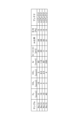
- FIG. 3 is a diagram showing the gas composition and pressure during film formation of each sample synthesized in Example 2.
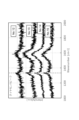
- FIG. 3 is a diagram showing the Raman scattering spectra of each sample synthesized in Example 2.
- FIG. 2 is a diagram showing the composition range of raw material gas in which diamond can be synthesized in a conventional CVD method.
- the film forming apparatus 100 of this embodiment is a plasma CVD apparatus that forms a carbon-based thin film on a base material W by a plasma CVD method using inductively coupled plasma P.
- the carbon-based thin film is, for example, a diamond film, a diamond-like carbon (DLC) film, or the like.
- the base material W of this embodiment is a plate-shaped material made of a material suitable for forming a carbon-based thin film.
- the base material W may be made of, for example, glass, plastic, silicon, iron, titanium, copper, metals such as cemented carbide, other alloy materials such as tool steel, materials such as SiC, GaN, AlN, BN, diamond, etc. These include, but are not limited to.
- the base material W has a rectangular or circular shape in plan view.
- the length of the base material W may be, for example, 20 cm or more or 50 cm or more, but is not limited thereto.
- the base material W may be, for example, a plurality of small chip-shaped base materials of about 1 mm, 5 mm, or 10 mm arranged with the same length or area.
- the base material W is not limited to a plate shape, but may be columnar, perforated, or porous. Further, it may have a complicated shape, such as tools such as drills and end mills.
- the base material W may be subjected to surface treatment such as so-called scratching treatment or seeding treatment.
- surface treatment such as so-called scratching treatment or seeding treatment.
- the base material W when the base material W is silicon, it may be immersed in alcohol together with diamond fine particles and subjected to a scratching process or a seeding process to form irregularities on the surface by ultrasonic treatment.
- the base material W is a cemented carbide
- the Co in the base material may be removed by immersing it in an acidic solution such as an aqueous nitric acid solution, or the surface of the WC (tungsten carbide) particles may be cleaned with an alkaline solution such as diluted NaOH. After the treatment, a seeding treatment as described above may be performed.
- the film forming apparatus 100 includes a vacuum container 2 that is evacuated and into which gas G is introduced, a gas supply mechanism 7 that supplies gas G to the vacuum container 2, and a gas supply mechanism 7 that supplies gas G to the vacuum container 2.
- the antenna 3 is provided with a linear antenna 3 disposed in the vacuum container 2, and a high frequency power source 4 that applies high frequency waves to the antenna 3 to generate inductively coupled plasma P within the vacuum container 2.
- a high frequency current IR flows through the antenna 3, an induced electric field is generated in the vacuum container 2, and an inductively coupled plasma P is generated. be done.
- the vacuum container 2 is a container made of metal such as SUS or aluminum, and the inside thereof is evacuated by a vacuum exhaust device 6.
- the vacuum container 2 is electrically grounded in this example.
- the vacuum evacuation device 6 includes a pressure regulator 61 such as a valve that regulates the pressure inside the vacuum container 2.
- the pressure regulator 61 is controlled to adjust the pressure inside the vacuum container 2 during plasma generation, for example, to a pressure of 7 Pa or more and 100 P or less.
- a gas G such as a raw material gas is introduced into the vacuum container 2 via, for example, a flow rate regulator (not shown) and a plurality of gas introduction ports 21 arranged in a direction along the antenna 3.
- a substrate holder 8 that holds the substrate W is provided inside the vacuum container 2, and a heater 81 that heats the substrate W is provided within the substrate holder 8.
- the film forming apparatus 100 of this embodiment has a function of adjusting the potential of the generated inductively coupled plasma in the range of, for example, +100V to -100V by applying a bias voltage from the bias power supply 9 to the substrate holder 8. It's okay.
- the applied bias voltage is, for example, a negative DC voltage, but is not limited to this.
- the energy when positive ions in the plasma P are incident on the base material W can be controlled to control the degree of crystallinity of a film formed on the surface of the base material W. I can do it.
- the gas supply mechanism 7 supplies gas G such as raw material gas into the vacuum container through the gas introduction port 21.
- the gas supply mechanism 7 is configured to supply the gas G downward from a gas introduction port 21 provided on the upper wall of the vacuum container 2 .
- This gas supply mechanism 7 is configured to be able to supply a raw material gas containing at least C (carbon), H (hydrogen), and O (oxygen), and specifically includes H 2 gas, CH 4 gas, and CO
- the structure is such that two gases can be supplied as raw material gases. Note that if the gas supply mechanism 7 is configured to be able to supply a raw material gas containing C, H, and O into the vacuum container 2, it may be used in addition to or in place of H2 gas, CH4 gas, and CO2 gas. Alternatively, any other gas may be supplied as the raw material gas.
- the gas supply mechanism 7 is configured to be able to supply H 2 gas, CH 4 gas, and CO 2 gas at arbitrary flow rates.
- the gas supply mechanism 7 of the present embodiment has a ratio of the concentration of O atoms to the total concentration of O atoms and H atoms (O /(O+H)) is, for example, 10 at % or more and 60 at % or less, so that the flow rate of each gas can be adjusted and supplied.
- the gas supply mechanism 7 is configured to be able to supply catalyst gas into the vacuum container 2 at an arbitrary flow rate along with the raw material gas.
- This catalyst gas functions as a catalyst during plasma generation and promotes decomposition of the raw material gas.
- the gas supply mechanism 7 has a ratio of, for example, 50% to 90%, preferably 75% or more to the total flow rate of all gases supplied into the vacuum container 2 (here, the total flow rate of raw material gas and catalyst gas).
- the structure is such that the catalyst gas can be supplied so that the amount is 90% or less.
- examples of this catalyst gas include rare gases such as Ar gas, He gas, and Ne gas.
- the antenna 3 is arranged above the base material W in the vacuum container 2 so as to follow the surface of the base material W.
- a plurality of linear antennas 3 are arranged in parallel along the base material W (for example, substantially parallel to the surface of the base material W). In this way, it is possible to generate plasma P with good uniformity over a wider range, and therefore it is possible to process a larger base material W.
- the number of antennas 3 is not limited to a plurality of antennas, and may be just one.
- the number is preferably an even number (for example, 2, 4, 6, etc.).
- the interval between each antenna 3 is preferably 5 cm or more, more preferably 10 cm or more, and even more preferably 15 cm or more.
- the spacing between the antennas 3 is preferably 25 cm or less.
- the plurality of antennas 3 are arranged parallel to each other and on the same plane, and the plane surrounded by the antennas 3 at both ends is square or rectangular (preferably, one side is 40 cm or more). More preferably, each side is 50 cm or more, still more preferably one side is 70 cm or more, and still more preferably one side is 100 cm or more.
- the vicinity of both ends of the antenna 3 penetrate a pair of opposing side walls 2a and 2b of the vacuum container 2, respectively.
- Insulating members 11 are provided at the portions where both ends of the antenna 3 are penetrated to the outside of the vacuum container 2 . Both ends of the antenna 3 pass through each insulating member 11, and the penetrating portion is vacuum-sealed with, for example, a packing 12.
- the antenna 3 is supported via the insulating member 11 while being electrically insulated from the opposing side walls 2a and 2b of the vacuum container 2.
- the space between each insulating member 11 and the vacuum container 2 is also vacuum-sealed by, for example, a packing 13.
- the material of the insulating member 11 is, for example, ceramics such as alumina, quartz, or engineering plastics such as polyphenylene sulfide (PPS) and polyether ether ketone (PEEK).
- the antenna 3 is a so-called LC antenna that includes an L section that serves as an inductor and a C section that serves as a capacitor.
- this antenna 3 includes at least two tubular metal conductor elements 31 (hereinafter referred to as metal pipes 31) and a tubular conductor element 31 that is provided between adjacent metal pipes 31 and insulates the metal pipes 31.
- the capacitor 33 is provided between an insulating element 32 (hereinafter referred to as an insulating pipe 32) and two adjacent metal pipes 31, and is electrically connected in series with these elements.
- the conductor element 31 functions as the L section
- the capacitor 33 functions as the C section.
- the number of metal pipes 31 is three, and the number of insulating pipes 32 and capacitors 33 is two each.
- the antenna 3 may have a configuration having four or more metal pipes 31, and in this case, the number of insulating pipes 32 and capacitors 33 are each one less than the number of metal pipes 31.
- the material of the metal pipe 31 is, for example, copper, aluminum, an alloy thereof, stainless steel, etc., but is not limited thereto.
- the antenna 3 may be made hollow and a coolant such as cooling water may be allowed to flow therein to cool the antenna 3.
- the insulating pipe 32 of this embodiment is formed from a single member, it is not limited to this.
- the material of the insulating pipe 32 is, for example, alumina, fluororesin, polyethylene (PE), engineering plastic (eg, polyphenylene sulfide (PPS), polyether ether ketone (PEEK), etc.).
- a portion of the antenna 3 located inside the vacuum container 2 is covered with a straight-tube-shaped insulating cover (antenna protection tube) 10. Both ends of this insulating cover 10 are supported by insulating members 11. Note that there is no need to seal between both ends of the insulating cover 10 and the insulating member 11. This is because even if the gas G enters the space inside the insulating cover 10, plasma P is usually not generated in the space because the space is small and the distance that electrons travel is short.
- the material of the insulating cover 10 is, for example, quartz, alumina, fluororesin, silicon nitride, silicon carbide, silicon, or the like.
- the insulating cover 10 By providing the insulating cover 10, it is possible to suppress charged particles in the plasma P from entering the metal pipe 31 constituting the antenna 3. It is possible to suppress an increase in the plasma potential, and also to suppress metal contamination on the plasma P and the base material W due to sputtering of the metal pipe 31 by charged particles (mainly ions). can.
- the length of the antenna 3 is, for example, preferably 20 cm or more, more preferably 50 cm or more, and even more preferably 100 cm or more. On the other hand, from the viewpoint of ensuring the strength of the insulating pipe 32, the length of the antenna 3 is preferably 1000 cm or less, more preferably 500 cm or less.
- the antenna 3 has a feeding end 3a to which high frequency power is fed in the antenna direction (longitudinal direction X) and a grounding end 3b that is grounded. Specifically, at both ends of each antenna 3 in the longitudinal direction This becomes the grounding end 3b.
- a high frequency is applied to the feeding end 3a of each antenna 3 from the high frequency power source 4 via the matching box 41.
- the frequency of the high frequency is 400 kHz or more and 100 MHz or less, for example, a common frequency of 13.56 MHz, but is not limited to this. For example, it may be 27.12 MHz, 40.68 MHz, 60 MHz, etc.
- a method for forming a carbon-based thin film using the film forming apparatus 100 described above will be described.
- a first film-forming method and a second film-forming method using different composition ratios of source gases to be supplied will be described.
- a carbon-based thin film such as diamond can be formed using any film forming method.
- the base material W is set in the base material holder 8 in the vacuum container 2 of the film forming apparatus 100, and the vacuum container 2 is evacuated by the vacuum evacuation device 6. It is preferable that the base material W is heated by the heater 81 and the temperature of the base material W is set to 100° C. or more and 1200° C. or less. The temperature range of the base material W may be changed depending on the grain size and crystallinity of the diamond to be synthesized. In the first film formation method, for example, when synthesizing a carbon-based thin film in which diamond microcrystals are present in a DLC film, it is preferable that the temperature of the base material W be 100° C. or more and 400° C. or less.
- the temperature of the base material W is preferably 200°C or more and less than 500°C.
- the temperature of the base material W is preferably 200° C. or more and less than 500° C.
- the temperature of the base material W is preferably 700° C. or more and 1200° C. or less.
- the gas supply mechanism 7 supplies H 2 gas, CH 4 gas, and CO 2 gas as raw material gases into the vacuum container 2 at a predetermined flow rate.
- the atomic ratio of O atoms, C atoms, and H atoms in the source gas falls within the diagonally shaded range shown in the composition ternary diagram (C-H-O diagram) in FIG. Then, adjust the flow rates of H 2 gas, CH 4 gas, and CO 2 gas. The atomic ratio of each atom will be explained below.
- the ratio of the concentration of O atoms to the total concentration of O atoms and H atoms contained is preferably 10 at% or more and 60 at% or less, more preferably 30 at%.
- the flow rates of H 2 gas, CH 4 gas, and CO 2 gas are controlled and supplied so that the amount is 50 at % or less.
- the ratio of the concentration of C atoms to the total concentration of O atoms and C atoms contained is preferably 30 at% or more and 45 at% or less, more preferably 35 at%.
- the flow rates of H 2 gas, CH 4 gas, and CO 2 gas are controlled and supplied so that the amount is 45 at % or less.
- the ratio of the concentration of H atoms to the total concentration of C atoms and H atoms contained is preferably 40 at% or more and 90 at% or less, more preferably 50 at%. % or more and 80 at % or less, the respective flow rates of H 2 gas, CH 4 gas, and CO 2 gas are controlled and supplied.
- the gas supply mechanism 7 supplies a catalyst gas such as Ar gas into the vacuum container along with the raw material gas.
- the flow rate of the catalyst gas to be supplied is set so that the ratio to the total flow rate of all gases supplied to the vacuum container 2 is preferably 50% or more and 90% or less, more preferably 75% or more and 90% or less. .
- energy can be transferred from, for example, Ar, which is easily ionized, to CH 4 , and a large amount of C 2 radicals, which can easily generate diamond, can be generated.
- the ratio of the emission intensity of C2 radicals to the emission intensity of H ⁇ radicals is set at 30% or more and 300% or less, more preferably 90% or more and 250% or less. % or less.
- the gas supply mechanism 7 introduces the raw material gas and the catalyst gas, and the pressure regulator 61 adjusts the pressure inside the vacuum container 2 to 7 Pa or more and 100 Pa or less, more preferably 10 Pa or more and 50 Pa or less.
- high-frequency power is supplied from the high-frequency power source 4 to the antenna 3 while the flow rates of the raw material gas and the catalyst gas are adjusted and the pressure inside the vacuum container 2 is adjusted as described above.
- an induced electric field is generated in the vacuum container 2 to generate inductively coupled plasma P, and a carbon-based thin film is formed on the base material W.
- the frequency of the high-frequency power is 400 kHz or more and 100 MHz or less, and preferably 13.56 MHz, for example.
- the power density of the high frequency power to be supplied is preferably 0.1 W/cm 2 or more, more preferably 0.5 W/cm 2 or more, and even more preferably 1 W/cm 2 or more. Further, the power density is preferably 1000 W/cm 2 or less, more preferably 100 W/cm 2 or less, and even more preferably 50 W/cm 2 or less.
- the base material W is set in the base material holder 8 in the vacuum container 2 of the film forming apparatus 100, and the vacuum container 2 is evacuated by the vacuum evacuation device 6. It is preferable that the base material W is heated by the heater 81 and the temperature of the base material W is set to 100° C. or more and 1200° C. or less. The temperature range of the base material W may be changed depending on the grain size and crystallinity of the diamond to be synthesized.
- the supplied raw material gas when synthesizing a carbon-based thin film containing diamond with a particle size of 50 nm or less, the supplied raw material gas is hydrogen-rich and the temperature of the base material W is set at 500°C or more and 1200°C or less. is preferable.
- the supplied raw material gas be enriched with oxygen and the temperature of the base material W be 800° C. or less.
- the gas supply mechanism 7 supplies H 2 gas, CH 4 gas, and CO 2 gas as raw material gases into the vacuum container 2 at a predetermined flow rate.
- the atomic ratio of O atoms, C atoms, and H atoms in the source gas falls within the diagonally shaded range shown in the composition ternary diagram (C-H-O diagram) in FIG. Then, adjust the flow rates of H 2 gas, CH 4 gas, and CO 2 gas. The atomic ratio of each atom will be explained below.
- the ratio of the concentration of O atoms to the total concentration of O atoms and H atoms contained is preferably 5 at% or more and 45 at% or less, more preferably 5 at%.
- the flow rates of H 2 gas, CH 4 gas, and CO 2 gas are controlled and supplied so that the amount is 10 at % or less.
- H 2 gas, CH 4 gas and CO 2 gas are controlled and supplied.
- the ratio of the concentration of H atoms to the total concentration of C atoms and H atoms contained is preferably 60 at% or more and 95 at% or less, more preferably 90 at%. % or more and 95 at % or less, the respective flow rates of H 2 gas, CH 4 gas, and CO 2 gas are controlled and supplied.
- the gas supply mechanism 7 supplies a catalyst gas such as Ar gas into the vacuum container along with the raw material gas.
- the flow rate of the catalyst gas to be supplied is such that the ratio to the total flow rate of all gases supplied to the vacuum container 2 is preferably 50% or more and 95% or less, more preferably 70% or more and 90% or less.
- the ratio of the emission intensity of C2 radicals to the emission intensity of H ⁇ radicals can be increased from 30% to 300% in the emission spectrum of the generated inductively coupled plasma.
- it can be set to 90% or more and 250% or less.
- the gas supply mechanism 7 introduces the raw material gas and the catalyst gas, and the pressure regulator 61 adjusts the pressure inside the vacuum container 2 to 7 Pa or more and 100 Pa or less, more preferably 10 Pa or more and 50 Pa or less.
- high-frequency power is supplied from the high-frequency power source 4 to the antenna 3 while the flow rates of the raw material gas and the catalyst gas are adjusted and the pressure inside the vacuum container 2 is adjusted as described above.
- an induced electric field is generated in the vacuum container 2 to generate inductively coupled plasma P, and a carbon-based thin film is formed on the base material W.
- the frequency of the high-frequency power is 400 kHz or more and 100 MHz or less, and preferably 13.56 MHz, for example.
- the power density of the high frequency power to be supplied is preferably 0.1 W/cm 2 or more, more preferably 0.5 W/cm 2 or more, and even more preferably 1 W/cm 2 or more. Further, the power density is preferably 1000 W/cm 2 or less, more preferably 100 W/cm 2 or less, and even more preferably 50 W/cm 2 or less.
- carbon-based thin films such as diamond can be formed using raw material gases with a wide composition range, which was not possible with methods using conventional CVD equipment, and carbon-based thin films with larger areas can be formed compared to conventional plasma CVD equipment. can do. Furthermore, by introducing Ar gas as a catalyst gas, the generation of C 2 radicals can also be promoted. A carbon-based thin film such as diamond can be easily formed on the base material W by forming a film on the base material W using these C 2 radicals and removing non-diamond components using oxygen-containing radicals and hydrogen radicals.
- the diamond peak intensity near 1333 cm -1 is the G-band peak near 1550 cm -1 .
- a diamond film having a strength of more than 20%, preferably 100% or more, and more preferably 1000% or more can be formed.
- the film forming apparatus 100 of the present invention is not limited to the above embodiment.
- the antenna 3 that generates inductively coupled plasma is placed inside the vacuum container 2, but the present invention is not limited to this.
- the film forming apparatus 100 of other embodiments may have a structure in which the antenna 3 is disposed outside the vacuum container 2.
- a high-frequency power source that supplies a high-frequency current to the antenna, and a gas supply mechanism that supplies a raw material gas containing C, H, and O into the vacuum container, and by flowing a high-frequency current to the antenna, the gas is supplied into the vacuum container.
- Aspect 2 The film forming apparatus according to Aspect 1, wherein the composition of the source gas supplied by the gas supply mechanism is such that the ratio of the concentration of O atoms to the total concentration of O atoms and H atoms is 10 at% or more and 60 at% or less. .
- the gas supply mechanism supplies a catalyst gas into the vacuum container together with the source gas, and sets the ratio of the flow rate of the catalyst gas to the total flow rate of all gases supplied into the vacuum container to be 50% or more and 90%.
- the diamond film has a diamond peak intensity near 1333 cm -1 that is more than 20% of a G-band peak intensity near 1550 cm -1 in Raman spectroscopy with 325 nm excitation.
- a source gas containing C, H, and O is supplied into a vacuum container in which a base material is placed, and the antennas are arranged inside or outside the vacuum container, and the antennas are electrically connected to each other in series.
- an inductively coupled plasma is generated in the vacuum container, and carbon is deposited on the base material by a plasma CVD method using the generated inductively coupled plasma.
- the carbon-based thin film is a diamond film, and the diamond film has a diamond peak intensity near 1333 cm -1 that is 20% of the G-band peak intensity near 1550 cm -1 in Raman spectroscopy with 325 nm excitation.
- Example 1 In Example 1, a plurality of samples (No. 1 to No. ) was deposited on the substrate. Moreover, sample No. A film of No. 11 was formed on the substrate.
- the flow rate of the source gas, the composition of the source gas, the flow rate ratio of Ar gas, and the pressure inside the vacuum container 2 during film formation of each sample are as shown in FIG.
- Other film forming conditions are as follows. ⁇ Frequency of high frequency power supplied: 13.56MHz ⁇ Power density of high frequency power supplied: 1.4W/ cm2 ⁇ Substrate temperature: 500°C
- FIG. 6 shows the Raman scattering spectra obtained for each sample.
- an LC antenna is used, and the ratio of the concentration of O atoms to the total concentration of O atoms and H atoms in the source gas is 10 at% or more and 60 at% or less, and the flow rate of Ar gas in the total gas is No. 1, in which the ratio is 50% or more and 90% or less, and the pressure inside the vacuum container 2 is 7Pa or more and 100Pa or less. 1 ⁇ No. In sample No. 4, an optical phonon peak of diamond was observed near the wavelength of 1333 cm -1 , confirming that diamond could be formed into a film.
- Example 2 In Example 2, a plurality of samples (No. 12 to No. 15) were prepared by changing the composition of the source gas, the pressure of the vacuum container 2, and the flow rate ratio of Ar gas by the plasma CVD method using the film forming apparatus 100 described above. ) was deposited on the substrate.
- the flow rate of the source gas, the composition of the source gas, the flow rate ratio of Ar gas, and the pressure inside the vacuum vessel 2 during film formation of each sample are as shown in FIG.
- Other film forming conditions are as follows. ⁇ Frequency of high frequency power supplied: 13.56MHz ⁇ Power density of high frequency power supplied: 1.4W/ cm2 ⁇ Substrate temperature: 500°C
- FIG. 8 shows the Raman scattering spectra obtained for each sample.
- the ratio of the concentration of O atoms to the total concentration of O atoms and H atoms is 5 at% or more and 45 at% or less, and the total concentration of O atoms and C atoms is The ratio of the concentration of C atoms to the total concentration of C atoms and H atoms is 45 at% to 70 at%, the ratio of the concentration of H atoms to the total concentration of C atoms and H atoms is 60 at% to 95 at%, and the flow rate of Ar gas in the total gas is No.
- a film forming apparatus that forms a carbon-based thin film such as diamond using the CVD method, it is possible to form a carbon-based thin film using a raw material gas having a wide composition range, and it is also possible to form a film over a large area. Become.
- Plasma CVD apparatus 2 Vacuum container 3
- Antenna 7 Gas supply mechanism W
- Base material P Base material
Landscapes
- Chemical & Material Sciences (AREA)
- Engineering & Computer Science (AREA)
- Physics & Mathematics (AREA)
- Plasma & Fusion (AREA)
- Materials Engineering (AREA)
- Organic Chemistry (AREA)
- Metallurgy (AREA)
- General Chemical & Material Sciences (AREA)
- Chemical Kinetics & Catalysis (AREA)
- Mechanical Engineering (AREA)
- Analytical Chemistry (AREA)
- Inorganic Chemistry (AREA)
- Spectroscopy & Molecular Physics (AREA)
- Electromagnetism (AREA)
- Public Health (AREA)
- Epidemiology (AREA)
- Crystallography & Structural Chemistry (AREA)
- Health & Medical Sciences (AREA)
- Chemical Vapour Deposition (AREA)
- Crystals, And After-Treatments Of Crystals (AREA)
- Plasma Technology (AREA)
Abstract
Description
前記した本発明の成膜装置では、このような原料ガスの組成範囲においても炭素系薄膜を形成することができる。
原料ガスと共にArガスを供給することにより、電離しやすいArが触媒となって原料ガスの分解を促進できる。これにより、炭素系薄膜を形成可能な原料ガスの組成範囲をより広範囲にすることができる。このような効果は、Arガスの流量割合を50%以上90%以下とすることで顕著になる。
Hαラジカルの発光強度に対するC2ラジカルの発光強度の比率が30%未満の場合、膜合成よりもエッチングが大きくなり核生成しない恐れがある。一方で、Hαラジカルの発光強度に対するC2ラジカルの発光強度の比率が300%超の場合、非ダイヤモンド成分が多くなり黒鉛やDLC膜となる恐れがある。
成膜時の真空容器内の圧力が7Pa未満の場合、合成した膜へのイオン衝撃が大きくなり黒鉛膜となる恐れがある。一方で、成膜時の真空容器内の圧力が100Pa超の場合、アンテナ周辺にプラズマが集中し炭素系薄膜を合成できない恐れがある。
本実施形態の成膜装置100は、誘導結合型のプラズマPを用いたプラズマCVD法により、基材W上に炭素系薄膜の形成を行うプラズマCVD装置である。ここで炭素系薄膜とは、例えばダイヤモンド膜、ダイヤモンドライクカーボン(DLC)膜等である。
次に上記した成膜装置100を用いた炭素系薄膜の成膜方法について説明する。以下、供給する原料ガスの組成比が異なる第1の成膜方法と第2の成膜方法を説明する。上記した成膜装置100によれば、いずれの成膜方法によってもダイヤモンド等の炭素系薄膜を形成することができる。
まず成膜装置100の真空容器内2に基材ホルダ8に基材Wをセットし、真空排気装置6により真空容器2を真空排気する。ヒータ81により基材Wを加熱し、基材Wの温度を100℃以上1200℃以下とするのが好ましい。基材Wの温度の範囲は、合成するダイヤモンドの粒径や結晶性によって変更してもよい。第1の成膜方法では、例えばDLC膜中にダイヤモンド微結晶が存在する炭素系薄膜を合成する場合には、基材Wの温度を100℃以上400℃以下とするのが好ましい。粒径200nm以下のダイヤモンドを含む炭素系薄膜を合成する場合には、基材Wの温度を200℃以上500℃未満とするのが好ましい。粒径200nm以上1000nm以下のダイヤモンドを含む炭素系薄膜を合成する場合には、基材Wの温度を200℃以上500℃未満とするのが好ましい。粒径1000nm以上のダイヤモンドを含む炭素系薄膜を合成する場合には、基材Wの温度を700℃以上1200℃以下とするのが好ましい。
次にガス供給機構7により、原料ガスとしてのH2ガス、CH4ガス及びCO2ガスを真空容器2内に所定の流量で供給する。本実施形態の成膜方法では、原料ガス中のO原子、C原子、H原子の原子数比率が、図2の組成三元図(C-H-Oダイアグラム)に示す斜線の範囲となるように、H2ガス、CH4ガス及びCO2ガスの各流量を調整する。各原子の原子数比率について以下に説明する。
供給する原料ガスにおいて、含有するO原子とH原子の合計濃度に対するO原子の濃度の割合(O/(O+H))が、好ましくは10at%以上60at%以下となるように、より好ましくは30at%以上50at%以下となるように、H2ガス、CH4ガス及びCO2ガスの各流量を制御して供給する。
供給する原料ガスにおいて、含有するO原子とC原子の合計濃度に対するC原子の濃度の割合(C/(O+C))が、好ましくは30at%以上45at%以下となるように、より好ましくは35at%以上45at%以下となるように、H2ガス、CH4ガス及びCO2ガスの各流量を制御して供給する。
また供給する原料ガスにおいて、含有するC原子とH原子の合計濃度に対するH原子の濃度の割合(H/(C+H))が、好ましくは40at%以上90at%以下となるように、より好ましくは50at%以上80at%以下となるように、H2ガス、CH4ガス及びCO2ガスの各流量を制御して供給する。
さらにガス供給機構7により、原料ガスとともに、Arガス等の触媒ガスを真空容器内に供給する。供給する触媒ガスの流量は、真空容器2に供給する全ガスの合計流量に対する割合が、好ましくは50%以上90%以下となるように、より好ましくは75%以上90%以下となるようにする。供給する触媒ガスの流量をこのような範囲にすることで、成膜時において、電離しやすい例えばArからCH4にエネルギーを受け渡し、ダイヤモンドを生成しやすいC2ラジカルを多く生成させることができる。これにより、図3に示すように、生成する誘導結合型プラズマの発光スペクトルにおいて、Hαラジカルの発光強度に対するC2ラジカルの発光強度の比率を30%以上300%以下、より好ましくは90%以上250%以下とすることができる。
そしてガス供給機構7により、原料ガス及び触媒ガスを導入しつつ、圧力調整器61により真空容器2内の圧力を7Pa以上100Pa以下、より好ましくは10Pa以上50Pa以下となるように調整する。
そして、上記のように原料ガス及び触媒ガスの流量を調整し、真空容器2内の圧力を調整した状態で、高周波電源4からアンテナ3に高周波電力を供給する。これにより真空容器2内に誘導電界を生じさせて誘導結合型のプラズマPを生成させ、基材Wに炭素系薄膜を形成する。高周波電力の周波数は、400kHz以上100MHz以下であり、例えば13.56MHzが望ましい。また供給する高周波電力の電力密度は、0.1W/cm2以上が好ましく、0.5W/cm2以上がより好ましく、1W/cm2以上がさらに好ましい。また電力密度は、1000W/cm2以下が好ましく、100W/cm2以下がより好ましく、50W/cm2以下がさらに好ましい。
次に、第1の成膜方法とは、供給する原料ガスのガス組成比が異なる第2の成膜方法を説明する。まず成膜装置100の真空容器内2に基材ホルダ8に基材Wをセットし、真空排気装置6により真空容器2を真空排気する。ヒータ81により基材Wを加熱し、基材Wの温度を100℃以上1200℃以下とするのが好ましい。基材Wの温度の範囲は、合成するダイヤモンドの粒径や結晶性によって変更してもよい。第2の成膜方法では、粒径50nm以下のダイヤモンドを含む炭素系薄膜を合成する場合には、供給する原料ガスを水素リッチにして、基材Wの温度を500℃以上1200℃以下とするのが好ましい。粒径10nm以下のダイヤモンドを含む炭素系薄膜を合成する場合には、供給する原料ガスを酸素リッチにして、基材Wの温度を800℃以下とするのが好ましい。
次にガス供給機構7により、原料ガスとしてのH2ガス、CH4ガス及びCO2ガスを真空容器2内に所定の流量で供給する。本実施形態の成膜方法では、原料ガス中のO原子、C原子、H原子の原子数比率が、図4の組成三元図(C-H-Oダイアグラム)に示す斜線の範囲となるように、H2ガス、CH4ガス及びCO2ガスの各流量を調整する。各原子の原子数比率について以下に説明する。
供給する原料ガスにおいて、含有するO原子とH原子の合計濃度に対するO原子の濃度の割合(O/(O+H))が、好ましくは5at%以上45at%以下となるように、より好ましくは5at%以上10at%以下となるように、H2ガス、CH4ガス及びCO2ガスの各流量を制御して供給する。
供給する原料ガスにおいて、含有するO原子とC原子の合計濃度に対するC原子の濃度の割合(C/(O+C))が、好ましくは45at%以上70at%以下となるように、H2ガス、CH4ガス及びCO2ガスの各流量を制御して供給する。
また供給する原料ガスにおいて、含有するC原子とH原子の合計濃度に対するH原子の濃度の割合(H/(C+H))が、好ましくは60at%以上95at%以下となるように、より好ましくは90at%以上95at%以下となるように、H2ガス、CH4ガス及びCO2ガスの各流量を制御して供給する。
さらにガス供給機構7により、原料ガスとともに、Arガス等の触媒ガスを真空容器内に供給する。供給する触媒ガスの流量は、真空容器2に供給する全ガスの合計流量に対する割合が、好ましくは50%以上95%以下、より好ましくは70%以上90%以下となるようにする。供給する触媒ガスの流量をこのような範囲にすることで、生成する誘導結合型プラズマの発光スペクトルにおいて、Hαラジカルの発光強度に対するC2ラジカルの発光強度の比率を30%以上300%以下、より好ましくは90%以上250%以下とすることができる。
そしてガス供給機構7により、原料ガス及び触媒ガスを導入しつつ、圧力調整器61により真空容器2内の圧力を7Pa以上100Pa以下、より好ましくは10Pa以上50Pa以下となるように調整する。
そして、上記のように原料ガス及び触媒ガスの流量を調整し、真空容器2内の圧力を調整した状態で、高周波電源4からアンテナ3に高周波電力を供給する。これにより真空容器2内に誘導電界を生じさせて誘導結合型のプラズマPを生成させ、基材Wに炭素系薄膜を形成する。高周波電力の周波数は、400kHz以上100MHz以下であり、例えば13.56MHzが望ましい。また供給する高周波電力の電力密度は、0.1W/cm2以上が好ましく、0.5W/cm2以上がより好ましく、1W/cm2以上がさらに好ましい。また電力密度は、1000W/cm2以下が好ましく、100W/cm2以下がより好ましく、50W/cm2以下がさらに好ましい。
このように構成された本実施形態の成膜装置100及び成膜方法によれば、高周波の誘導電界により生成した誘導結合型のプラズマPを用いることで、原料ガスに含まれる結合エネルギーが高い分子であるCO2等の分解が広範囲にわたって可能となり、酸素含有ラジカルの生成を促進できる。さらに、アンテナ3により誘導結合プラズマを生成する構成としているため、原料ガスが酸素を多く含むガス組成であっても、長時間の活性化を可能にできる。これにより、従来のCVD装置を用いた方法では実現できなかった広い組成範囲の原料ガスでダイヤモンド等の炭素系薄膜を形成でき、しかも従来のプラズマCVD装置に比べて大面積の炭素系薄膜を形成することができる。
また触媒ガスとしてArガスを導入することによりC2ラジカルの生成も促進できる。このC2ラジカル等によって基材W上に膜を形成し、酸素含有ラジカルおよび水素ラジカルによって非ダイヤモンド成分を除去することで、ダイヤモンド等の炭素系薄膜を基材W上に形成しやすくできる。
例えば、前記実施形態の成膜装置100は、誘導結合型プラズマを生成するアンテナ3は真空容器2内に配置されていたが、これに限らない。他の実施形態の成膜装置100は、真空容器2の外部にアンテナ3を配置した構造であってもよい。
以下、実施例を挙げて本発明をより具体的に説明する。本発明は以下の実施例によって制限を受けるものではなく、前記、後記の趣旨に適合し得る範囲で変更を加えて実施することも可能であり、それらはいずれも本発明の技術的範囲に包含される。
実施例1では、前記した成膜装置100を用いたプラズマCVD法により、原料ガスの組成、真空容器2の圧力及びArガスの流量比率を変えて、複数のサンプル(No.1~No.10)を基板上に成膜した。また、LCアンテナではない(すなわちコンデンサ部を備えない)単純な直線状アンテナを用いた成膜装置を用いてサンプルNo.11を基板上に成膜した。各サンプルの成膜時における原料ガスの流量、原料ガスの組成、Arガスの流量比率、及び真空容器2内の圧力は、図5に示すとおりである。その他の成膜条件は、次のとおりである。
・供給する高周波電力の周波数:13.56MHz
・供給する高周波電力の電力密度:1.4W/cm2
・基板温度:500℃
実施例2では、前記した成膜装置100を用いたプラズマCVD法により、原料ガスの組成、真空容器2の圧力及びArガスの流量比率を変えて、複数のサンプル(No.12~No.15)を基板上に成膜した。各サンプルの成膜時における原料ガスの流量、原料ガスの組成、Arガスの流量比率、及び真空容器2内の圧力は、図7に示すとおりである。その他の成膜条件は、次のとおりである。
・供給する高周波電力の周波数:13.56MHz
・供給する高周波電力の電力密度:1.4W/cm2
・基板温度:500℃
2・・・真空容器
3・・・アンテナ
7・・・ガス供給機構
W・・・基材
P・・・プラズマ
Claims (11)
- 基材が配置される真空容器と、
前記真空容器内に誘導結合型プラズマを発生させるものであって、電気的に互いに直列接続された導体要素と容量素子とを有するアンテナと、
前記アンテナに高周波電流を供給する高周波電源と、
前記真空容器内にC、H及びOを含む原料ガスを供給するガス供給機構とを備え、
前記アンテナに高周波電流を流すことによって当該真空容器内に生じる誘導結合型プラズマを用いたプラズマCVD法により前記真空容器内の前記基材上に炭素系薄膜を形成する成膜装置。 - 前記ガス供給機構が供給する前記原料ガスの組成は、O原子とH原子の合計濃度に対するO原子の濃度の割合が10at%以上60at%以下である請求項1に記載の成膜装置。
- 前記ガス供給機構が前記原料ガスとともに触媒ガスを前記真空容器内に供給し、前記真空容器内に供給する全ガスの合計流量に対する前記触媒ガスの流量の割合を50%以上90%以下とする請求項1に記載の成膜装置。
- 前記触媒ガスがArガスである請求項3に記載の成膜装置。
- 前記誘導結合型プラズマの発光スペクトルは、Hαラジカルの発光強度に対するC2ラジカルの発光強度の比率が30%以上300%以下である請求項1に記載の成膜装置。
- 成膜時における前記真空容器内の圧力が7Pa以上100Pa以下である請求項1に記載の成膜装置。
- 前記アンテナが直線状をなし、長さが20cm以上のものである請求項1に記載の成膜装置。
- 前記炭素系薄膜がダイヤモンド膜である請求項1に記載の成膜装置。
- 前記ダイヤモンド膜は、325nm励起のラマン分光分析において、1333cm-1付近のダイヤモンドのピーク強度が1550cm-1付近のGバンドのピーク強度の20%超である請求項1に記載の成膜装置。
- 基材が配置された真空容器内にC、H及びOを含有する原料ガスを供給し、
前記真空容器の内部又は外部に配置したアンテナであって、電気的に互いに直列接続された導体要素と容量素子とを有するアンテナに高周波電流を流すことによって当該真空容器内に誘導結合型プラズマを生成し、
生成した誘導結合型プラズマを用いたプラズマCVD法により、前記基材上に炭素系薄膜を形成する成膜方法。 - 前記炭素系薄膜がダイヤモンド膜であり、当該ダイヤモンド膜は、325nm励起のラマン分光分析において、1333cm-1付近のダイヤモンドのピーク強度が1550cm-1付近のGバンドのピーク強度の20%超である請求項10に記載の成膜方法。
Priority Applications (5)
| Application Number | Priority Date | Filing Date | Title |
|---|---|---|---|
| CN202380016467.2A CN118510939A (zh) | 2022-05-10 | 2023-04-27 | 成膜装置及成膜方法 |
| DE112023002182.1T DE112023002182T5 (de) | 2022-05-10 | 2023-04-27 | Filmbildungsvorrichtung und Filmbildungsverfahren |
| JP2024520396A JP7749173B2 (ja) | 2022-05-10 | 2023-04-27 | 成膜装置及び成膜方法 |
| GB2409339.5A GB2632050A (en) | 2022-05-10 | 2023-04-27 | Film forming device and film forming method |
| US18/833,913 US20250129480A1 (en) | 2022-05-10 | 2023-04-27 | Film forming device and film forming method |
Applications Claiming Priority (2)
| Application Number | Priority Date | Filing Date | Title |
|---|---|---|---|
| JP2022077363 | 2022-05-10 | ||
| JP2022-077363 | 2022-05-10 |
Publications (1)
| Publication Number | Publication Date |
|---|---|
| WO2023218990A1 true WO2023218990A1 (ja) | 2023-11-16 |
Family
ID=88730416
Family Applications (1)
| Application Number | Title | Priority Date | Filing Date |
|---|---|---|---|
| PCT/JP2023/016688 Ceased WO2023218990A1 (ja) | 2022-05-10 | 2023-04-27 | 成膜装置及び成膜方法 |
Country Status (6)
| Country | Link |
|---|---|
| US (1) | US20250129480A1 (ja) |
| JP (1) | JP7749173B2 (ja) |
| CN (1) | CN118510939A (ja) |
| DE (1) | DE112023002182T5 (ja) |
| GB (1) | GB2632050A (ja) |
| WO (1) | WO2023218990A1 (ja) |
Cited By (1)
| Publication number | Priority date | Publication date | Assignee | Title |
|---|---|---|---|---|
| WO2026004639A1 (ja) * | 2024-06-26 | 2026-01-02 | 日新電機株式会社 | 金属加工工具及び金属加工工具の製造方法 |
Citations (3)
| Publication number | Priority date | Publication date | Assignee | Title |
|---|---|---|---|---|
| JP2005088452A (ja) * | 2003-09-18 | 2005-04-07 | Dainippon Printing Co Ltd | ガスバリア性フィルム及びそれを用いてなる積層体 |
| JP2015183250A (ja) * | 2014-03-25 | 2015-10-22 | 株式会社Screenホールディングス | 成膜装置および成膜方法 |
| JP2020087891A (ja) * | 2018-11-30 | 2020-06-04 | 日新電機株式会社 | アンテナ及び成膜装置 |
Family Cites Families (5)
| Publication number | Priority date | Publication date | Assignee | Title |
|---|---|---|---|---|
| JP6471515B2 (ja) * | 2015-01-28 | 2019-02-20 | 日新電機株式会社 | パイプ保持接続構造およびそれを備える高周波アンテナ装置 |
| CN110291847A (zh) * | 2017-02-16 | 2019-09-27 | 日新电机株式会社 | 等离子体产生用的天线、具有所述天线的等离子体处理装置以及天线构造 |
| CN113632592A (zh) * | 2019-03-20 | 2021-11-09 | 日新电机株式会社 | 等离子体处理装置 |
| US12288672B2 (en) * | 2020-01-15 | 2025-04-29 | Applied Materials, Inc. | Methods and apparatus for carbon compound film deposition |
| US20220127721A1 (en) * | 2020-10-23 | 2022-04-28 | Applied Materials, Inc. | Depositing Low Roughness Diamond Films |
-
2023
- 2023-04-27 DE DE112023002182.1T patent/DE112023002182T5/de active Pending
- 2023-04-27 US US18/833,913 patent/US20250129480A1/en active Pending
- 2023-04-27 WO PCT/JP2023/016688 patent/WO2023218990A1/ja not_active Ceased
- 2023-04-27 GB GB2409339.5A patent/GB2632050A/en active Pending
- 2023-04-27 JP JP2024520396A patent/JP7749173B2/ja active Active
- 2023-04-27 CN CN202380016467.2A patent/CN118510939A/zh active Pending
Patent Citations (3)
| Publication number | Priority date | Publication date | Assignee | Title |
|---|---|---|---|---|
| JP2005088452A (ja) * | 2003-09-18 | 2005-04-07 | Dainippon Printing Co Ltd | ガスバリア性フィルム及びそれを用いてなる積層体 |
| JP2015183250A (ja) * | 2014-03-25 | 2015-10-22 | 株式会社Screenホールディングス | 成膜装置および成膜方法 |
| JP2020087891A (ja) * | 2018-11-30 | 2020-06-04 | 日新電機株式会社 | アンテナ及び成膜装置 |
Non-Patent Citations (2)
| Title |
|---|
| ANONYMOUS: "About ``Raman spectroscopy'' useful for DLC film evaluation.", MANAGEMENT & TECHNOLOGY FOR CREATIVE KYOTO, 1 April 2011 (2011-04-01), pages 17, XP093107535 * |
| SAKAI T., M. FUJIWARA, D. AZUMA, S. NAKATA, K. IRISAWA, K. KUBOTA, Y. ANDOH : "Development of CVD Apparatus for Manufacturing Flat Panel Displays ", NISSIN ELECTRIC, vol. 63, no. 1, 1 April 2018 (2018-04-01), pages 35 - 40, XP093107530 * |
Cited By (1)
| Publication number | Priority date | Publication date | Assignee | Title |
|---|---|---|---|---|
| WO2026004639A1 (ja) * | 2024-06-26 | 2026-01-02 | 日新電機株式会社 | 金属加工工具及び金属加工工具の製造方法 |
Also Published As
| Publication number | Publication date |
|---|---|
| JP7749173B2 (ja) | 2025-10-06 |
| GB202409339D0 (en) | 2024-08-14 |
| US20250129480A1 (en) | 2025-04-24 |
| CN118510939A (zh) | 2024-08-16 |
| JPWO2023218990A1 (ja) | 2023-11-16 |
| GB2632050A (en) | 2025-01-22 |
| DE112023002182T5 (de) | 2025-04-30 |
Similar Documents
| Publication | Publication Date | Title |
|---|---|---|
| JP3167938B2 (ja) | 表面のプラズマ処理のための方法及び装置 | |
| US5039548A (en) | Plasma chemical vapor reaction method employing cyclotron resonance | |
| US5368897A (en) | Method for arc discharge plasma vapor deposition of diamond | |
| US7632379B2 (en) | Plasma source and plasma processing apparatus | |
| Mitsuda et al. | Development of a new microwave plasma torch and its application to diamond synthesis | |
| US5980999A (en) | Method of manufacturing thin film and method for performing precise working by radical control and apparatus for carrying out such methods | |
| EP2573047B1 (en) | Method for producing onion-like carbon | |
| JPH04232274A (ja) | Cvdダイヤモンドによるドリルの被覆法 | |
| JP7749173B2 (ja) | 成膜装置及び成膜方法 | |
| KR20180000721A (ko) | 성형된 피처리물 지지체를 갖는 토로이달 플라즈마 처리 장치 | |
| JP2020105040A (ja) | 基板上のグラフェン膜の直接成膜法及び走査型プローブ顕微鏡用カンチレバー | |
| JPWO2006043433A1 (ja) | プラズマcvd装置 | |
| WO2025009325A1 (ja) | ダイヤモンド薄膜の製造方法及びダイヤモンド薄膜製造装置 | |
| JP2025002656A (ja) | ダイヤモンド薄膜及びダイヤモンド薄膜の製造方法 | |
| JP5039120B2 (ja) | プラズマ処理装置用のアルミナ部材及びプラズマ処理装置用のアルミナ部材の製造方法 | |
| TWI429779B (zh) | 鑽石成核方法 | |
| WO2026004639A1 (ja) | 金属加工工具及び金属加工工具の製造方法 | |
| JPH0812492A (ja) | 気相合成装置および気相合成方法 | |
| RU214891U1 (ru) | Устройство для газоструйного осаждения алмазных покрытий | |
| RU2792526C1 (ru) | Устройство для нанесения алмазных покрытий | |
| JPH031377B2 (ja) | ||
| JPH0532489A (ja) | プラズマを用いるダイヤモンドの合成法 | |
| DE69615677T2 (de) | Verfahren zur Oberflächen-Plasmabearbeitung | |
| JPS6265997A (ja) | ダイヤモンド合成方法およびその装置 | |
| JPH0649635B2 (ja) | ダイヤモンドの合成方法 |
Legal Events
| Date | Code | Title | Description |
|---|---|---|---|
| 121 | Ep: the epo has been informed by wipo that ep was designated in this application |
Ref document number: 23803469 Country of ref document: EP Kind code of ref document: A1 |
|
| ENP | Entry into the national phase |
Ref document number: 2024520396 Country of ref document: JP Kind code of ref document: A |
|
| ENP | Entry into the national phase |
Ref document number: 202409339 Country of ref document: GB Kind code of ref document: A Free format text: PCT FILING DATE = 20230427 |
|
| WWE | Wipo information: entry into national phase |
Ref document number: 2409339.5 Country of ref document: GB |
|
| WWE | Wipo information: entry into national phase |
Ref document number: 202380016467.2 Country of ref document: CN |
|
| WWE | Wipo information: entry into national phase |
Ref document number: 18833913 Country of ref document: US |
|
| WWE | Wipo information: entry into national phase |
Ref document number: 112023002182 Country of ref document: DE |
|
| WWP | Wipo information: published in national office |
Ref document number: 2409339.5 Country of ref document: GB |
|
| WWP | Wipo information: published in national office |
Ref document number: 18833913 Country of ref document: US |
|
| WWP | Wipo information: published in national office |
Ref document number: 112023002182 Country of ref document: DE |
|
| 122 | Ep: pct application non-entry in european phase |
Ref document number: 23803469 Country of ref document: EP Kind code of ref document: A1 |