WO2023195325A1 - パワーモジュールおよび電力変換装置 - Google Patents
パワーモジュールおよび電力変換装置 Download PDFInfo
- Publication number
- WO2023195325A1 WO2023195325A1 PCT/JP2023/010614 JP2023010614W WO2023195325A1 WO 2023195325 A1 WO2023195325 A1 WO 2023195325A1 JP 2023010614 W JP2023010614 W JP 2023010614W WO 2023195325 A1 WO2023195325 A1 WO 2023195325A1
- Authority
- WO
- WIPO (PCT)
- Prior art keywords
- power module
- conductor layer
- power
- ceramic substrate
- region
- Prior art date
- Legal status (The legal status is an assumption and is not a legal conclusion. Google has not performed a legal analysis and makes no representation as to the accuracy of the status listed.)
- Ceased
Links
Images







Classifications
-
- H—ELECTRICITY
- H10—SEMICONDUCTOR DEVICES; ELECTRIC SOLID-STATE DEVICES NOT OTHERWISE PROVIDED FOR
- H10W—GENERIC PACKAGES, INTERCONNECTIONS, CONNECTORS OR OTHER CONSTRUCTIONAL DETAILS OF DEVICES COVERED BY CLASS H10
- H10W90/00—Package configurations
-
- H—ELECTRICITY
- H02—GENERATION; CONVERSION OR DISTRIBUTION OF ELECTRIC POWER
- H02M—APPARATUS FOR CONVERSION BETWEEN AC AND AC, BETWEEN AC AND DC, OR BETWEEN DC AND DC, AND FOR USE WITH MAINS OR SIMILAR POWER SUPPLY SYSTEMS; CONVERSION OF DC OR AC INPUT POWER INTO SURGE OUTPUT POWER; CONTROL OR REGULATION THEREOF
- H02M7/00—Conversion of AC power input into DC power output; Conversion of DC power input into AC power output
- H02M7/42—Conversion of DC power input into AC power output without possibility of reversal
- H02M7/44—Conversion of DC power input into AC power output without possibility of reversal by static converters
- H02M7/48—Conversion of DC power input into AC power output without possibility of reversal by static converters using discharge tubes with control electrode or semiconductor devices with control electrode
- H02M7/53—Conversion of DC power input into AC power output without possibility of reversal by static converters using discharge tubes with control electrode or semiconductor devices with control electrode using devices of a triode or transistor type requiring continuous application of a control signal
- H02M7/537—Conversion of DC power input into AC power output without possibility of reversal by static converters using discharge tubes with control electrode or semiconductor devices with control electrode using devices of a triode or transistor type requiring continuous application of a control signal using semiconductor devices only, e.g. single switched pulse inverters
- H02M7/5387—Conversion of DC power input into AC power output without possibility of reversal by static converters using discharge tubes with control electrode or semiconductor devices with control electrode using devices of a triode or transistor type requiring continuous application of a control signal using semiconductor devices only, e.g. single switched pulse inverters in a bridge configuration
-
- H—ELECTRICITY
- H10—SEMICONDUCTOR DEVICES; ELECTRIC SOLID-STATE DEVICES NOT OTHERWISE PROVIDED FOR
- H10W—GENERIC PACKAGES, INTERCONNECTIONS, CONNECTORS OR OTHER CONSTRUCTIONAL DETAILS OF DEVICES COVERED BY CLASS H10
- H10W40/00—Arrangements for thermal protection or thermal control
- H10W40/10—Arrangements for heating
-
- H—ELECTRICITY
- H10—SEMICONDUCTOR DEVICES; ELECTRIC SOLID-STATE DEVICES NOT OTHERWISE PROVIDED FOR
- H10W—GENERIC PACKAGES, INTERCONNECTIONS, CONNECTORS OR OTHER CONSTRUCTIONAL DETAILS OF DEVICES COVERED BY CLASS H10
- H10W40/00—Arrangements for thermal protection or thermal control
- H10W40/20—Arrangements for cooling
- H10W40/22—Arrangements for cooling characterised by their shape, e.g. having conical or cylindrical projections
- H10W40/226—Arrangements for cooling characterised by their shape, e.g. having conical or cylindrical projections characterised by projecting parts, e.g. fins to increase surface area
-
- H—ELECTRICITY
- H10—SEMICONDUCTOR DEVICES; ELECTRIC SOLID-STATE DEVICES NOT OTHERWISE PROVIDED FOR
- H10W—GENERIC PACKAGES, INTERCONNECTIONS, CONNECTORS OR OTHER CONSTRUCTIONAL DETAILS OF DEVICES COVERED BY CLASS H10
- H10W40/00—Arrangements for thermal protection or thermal control
- H10W40/20—Arrangements for cooling
- H10W40/25—Arrangements for cooling characterised by their materials
- H10W40/255—Arrangements for cooling characterised by their materials having a laminate or multilayered structure, e.g. direct bond copper [DBC] ceramic substrates
-
- H—ELECTRICITY
- H10—SEMICONDUCTOR DEVICES; ELECTRIC SOLID-STATE DEVICES NOT OTHERWISE PROVIDED FOR
- H10W—GENERIC PACKAGES, INTERCONNECTIONS, CONNECTORS OR OTHER CONSTRUCTIONAL DETAILS OF DEVICES COVERED BY CLASS H10
- H10W70/00—Package substrates; Interposers; Redistribution layers [RDL]
- H10W70/60—Insulating or insulated package substrates; Interposers; Redistribution layers
- H10W70/611—Insulating or insulated package substrates; Interposers; Redistribution layers for connecting multiple chips together
-
- H—ELECTRICITY
- H10—SEMICONDUCTOR DEVICES; ELECTRIC SOLID-STATE DEVICES NOT OTHERWISE PROVIDED FOR
- H10W—GENERIC PACKAGES, INTERCONNECTIONS, CONNECTORS OR OTHER CONSTRUCTIONAL DETAILS OF DEVICES COVERED BY CLASS H10
- H10W70/00—Package substrates; Interposers; Redistribution layers [RDL]
- H10W70/60—Insulating or insulated package substrates; Interposers; Redistribution layers
- H10W70/67—Insulating or insulated package substrates; Interposers; Redistribution layers characterised by their insulating layers or insulating parts
- H10W70/68—Shapes or dispositions thereof
- H10W70/685—Shapes or dispositions thereof comprising multiple insulating layers
-
- H—ELECTRICITY
- H10—SEMICONDUCTOR DEVICES; ELECTRIC SOLID-STATE DEVICES NOT OTHERWISE PROVIDED FOR
- H10W—GENERIC PACKAGES, INTERCONNECTIONS, CONNECTORS OR OTHER CONSTRUCTIONAL DETAILS OF DEVICES COVERED BY CLASS H10
- H10W76/00—Containers; Fillings or auxiliary members therefor; Seals
- H10W76/10—Containers or parts thereof
- H10W76/12—Containers or parts thereof characterised by their shape
- H10W76/15—Containers comprising an insulating or insulated base
-
- H—ELECTRICITY
- H10—SEMICONDUCTOR DEVICES; ELECTRIC SOLID-STATE DEVICES NOT OTHERWISE PROVIDED FOR
- H10W—GENERIC PACKAGES, INTERCONNECTIONS, CONNECTORS OR OTHER CONSTRUCTIONAL DETAILS OF DEVICES COVERED BY CLASS H10
- H10W76/00—Containers; Fillings or auxiliary members therefor; Seals
- H10W76/40—Fillings or auxiliary members in containers, e.g. centering rings
- H10W76/42—Fillings
- H10W76/47—Solid or gel fillings
-
- H—ELECTRICITY
- H10—SEMICONDUCTOR DEVICES; ELECTRIC SOLID-STATE DEVICES NOT OTHERWISE PROVIDED FOR
- H10W—GENERIC PACKAGES, INTERCONNECTIONS, CONNECTORS OR OTHER CONSTRUCTIONAL DETAILS OF DEVICES COVERED BY CLASS H10
- H10W90/00—Package configurations
- H10W90/701—Package configurations characterised by the relative positions of pads or connectors relative to package parts
-
- H—ELECTRICITY
- H10—SEMICONDUCTOR DEVICES; ELECTRIC SOLID-STATE DEVICES NOT OTHERWISE PROVIDED FOR
- H10W—GENERIC PACKAGES, INTERCONNECTIONS, CONNECTORS OR OTHER CONSTRUCTIONAL DETAILS OF DEVICES COVERED BY CLASS H10
- H10W72/00—Interconnections or connectors in packages
- H10W72/071—Connecting or disconnecting
- H10W72/073—Connecting or disconnecting of die-attach connectors
- H10W72/07331—Connecting techniques
- H10W72/07336—Soldering or alloying
-
- H—ELECTRICITY
- H10—SEMICONDUCTOR DEVICES; ELECTRIC SOLID-STATE DEVICES NOT OTHERWISE PROVIDED FOR
- H10W—GENERIC PACKAGES, INTERCONNECTIONS, CONNECTORS OR OTHER CONSTRUCTIONAL DETAILS OF DEVICES COVERED BY CLASS H10
- H10W72/00—Interconnections or connectors in packages
- H10W72/30—Die-attach connectors
- H10W72/351—Materials of die-attach connectors
- H10W72/352—Materials of die-attach connectors comprising metals or metalloids, e.g. solders
-
- H—ELECTRICITY
- H10—SEMICONDUCTOR DEVICES; ELECTRIC SOLID-STATE DEVICES NOT OTHERWISE PROVIDED FOR
- H10W—GENERIC PACKAGES, INTERCONNECTIONS, CONNECTORS OR OTHER CONSTRUCTIONAL DETAILS OF DEVICES COVERED BY CLASS H10
- H10W74/00—Encapsulations, e.g. protective coatings
- H10W74/40—Encapsulations, e.g. protective coatings characterised by their materials
- H10W74/47—Encapsulations, e.g. protective coatings characterised by their materials comprising organic materials, e.g. plastics or resins
- H10W74/473—Encapsulations, e.g. protective coatings characterised by their materials comprising organic materials, e.g. plastics or resins containing a filler
-
- H—ELECTRICITY
- H10—SEMICONDUCTOR DEVICES; ELECTRIC SOLID-STATE DEVICES NOT OTHERWISE PROVIDED FOR
- H10W—GENERIC PACKAGES, INTERCONNECTIONS, CONNECTORS OR OTHER CONSTRUCTIONAL DETAILS OF DEVICES COVERED BY CLASS H10
- H10W90/00—Package configurations
- H10W90/701—Package configurations characterised by the relative positions of pads or connectors relative to package parts
- H10W90/751—Package configurations characterised by the relative positions of pads or connectors relative to package parts of bond wires
- H10W90/753—Package configurations characterised by the relative positions of pads or connectors relative to package parts of bond wires between laterally-adjacent chips
-
- H—ELECTRICITY
- H10—SEMICONDUCTOR DEVICES; ELECTRIC SOLID-STATE DEVICES NOT OTHERWISE PROVIDED FOR
- H10W—GENERIC PACKAGES, INTERCONNECTIONS, CONNECTORS OR OTHER CONSTRUCTIONAL DETAILS OF DEVICES COVERED BY CLASS H10
- H10W90/00—Package configurations
- H10W90/701—Package configurations characterised by the relative positions of pads or connectors relative to package parts
- H10W90/751—Package configurations characterised by the relative positions of pads or connectors relative to package parts of bond wires
- H10W90/754—Package configurations characterised by the relative positions of pads or connectors relative to package parts of bond wires between a chip and a stacked insulating package substrate, interposer or RDL
-
- H—ELECTRICITY
- H10—SEMICONDUCTOR DEVICES; ELECTRIC SOLID-STATE DEVICES NOT OTHERWISE PROVIDED FOR
- H10W—GENERIC PACKAGES, INTERCONNECTIONS, CONNECTORS OR OTHER CONSTRUCTIONAL DETAILS OF DEVICES COVERED BY CLASS H10
- H10W90/00—Package configurations
- H10W90/701—Package configurations characterised by the relative positions of pads or connectors relative to package parts
- H10W90/751—Package configurations characterised by the relative positions of pads or connectors relative to package parts of bond wires
- H10W90/755—Package configurations characterised by the relative positions of pads or connectors relative to package parts of bond wires between a chip and a laterally-adjacent insulating package substrate, interpose or RDL
Definitions
- the present disclosure relates to a power module and a power conversion device.
- Power modules are installed in all kinds of products, including industrial equipment, home appliances, and information terminals, and high productivity is required of power modules.
- Power modules installed in electric vehicles are required to have high heat dissipation, and high flatness is required to ensure secure connection to the water cooling jacket.
- SiC semiconductors which are likely to become mainstream in the future.
- Patent Document 1 proposes a power module structure in which a semiconductor element is mounted on a ceramic substrate, a circuit is formed by wire bonding, and pin terminals are used as external terminals.
- Patent Document 1 a surface conductor layer that serves as a circuit pattern is provided on the top surface of the ceramic substrate for mounting semiconductor elements and pin terminals, but a back surface conductor layer is provided on the bottom surface of the ceramic substrate. are provided almost all over the area.
- the element size exceeds 10 mm square, and in the case of a 6in1 module, the number of elements is 12, and the ceramic substrate size is large at 60 mm to 70 mm square.
- the heat dissipation member When a large ceramic substrate is bonded to a copper or aluminum heat dissipation member, the heat dissipation member is excessively warped due to the large difference in linear expansion coefficient between the ceramic substrate and the heat dissipation member.
- water cooling liquid cooling
- warping can be suppressed to some extent by tightening screws or the like, it is necessary to further suppress warping in order to evenly apply deforming pressure to the O-ring to obtain watertightness.
- an object of the present disclosure is to provide a technology that can suppress warping of a heat dissipation member caused by thermal stress in a power module.
- a power module includes a semiconductor element, an insulating substrate having a mounting surface on which the semiconductor element is mounted, and a heat dissipation member bonded to a surface of the insulating substrate opposite to the mounting surface,
- the bonding area with the heat dissipating member on the insulating substrate is an area corresponding to the part on which the semiconductor element is mounted, and the area of the bonding area with the heat dissipating member on the insulating substrate corresponds to the area on which the semiconductor element is mounted. smaller than the area of the part.
- the present disclosure by reducing the area of the bonding region of the insulating substrate with the heat dissipating member, it is possible to suppress warpage of the heat dissipating member caused by thermal stress.
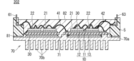
- FIG. 2 is a cross-sectional view of the power module according to the first embodiment.
- FIG. 3 is a top view showing the power module according to the first embodiment with the sealing resin removed.
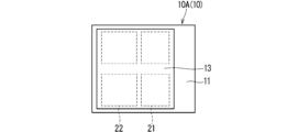
- FIG. 3 is a bottom view of a ceramic substrate included in the power module according to the first embodiment.
- FIG. 3 is a bottom view showing another example of the ceramic substrate included in the power module according to the first embodiment.
- 7 is a bottom view showing still another example of the ceramic substrate included in the power module according to the first embodiment.
- FIG. 1 is a schematic diagram showing a manufacturing process of a power module according to Embodiment 1.
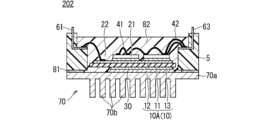
- FIG. FIG. 3 is a cross-sectional view of a power module according to Modification 1 of Embodiment 1.
- FIG. 7 is a cross-sectional view of a power module according to a second modification of the first embodiment.
- FIG. FIG. 7 is a top view showing a state in which a sealing resin is removed from a power module according to a second modification of the first embodiment.
- 7 is a bottom view of a ceramic substrate included in a power module according to a second modification of the first embodiment.
- FIG. FIG. 3 is a cross-sectional view of a power module according to a second embodiment.
- FIG. 3 is a bottom view of a ceramic substrate included in a power module according to a second embodiment.
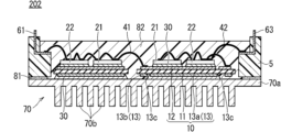
- FIG. 3 is a cross-sectional view of a power module according to a third embodiment.
- FIG. 7 is a bottom view of a ceramic substrate included in the power module according to Embodiment 3.
- FIG. 3 is a block diagram showing the configuration of a power conversion system to which a power conversion device according to a fourth embodiment is applied.
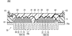
- FIG. 1 is a cross-sectional view of a power module 202 according to the first embodiment.
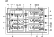
- FIG. 2 is a top view showing the power module 202 according to the first embodiment with the sealing resin 82 removed.
- the power module 202 is a 6-in-1 module, and includes six sets of semiconductor elements 21 and 22, two ceramic substrates 10A and 10B, a case 5, and a plurality of external electrodes 61. It includes a plurality of signal electrodes 63, a sealing resin 82, and a fin base 70.
- the ceramic substrate 10 corresponds to an insulating substrate
- the fin base 70 corresponds to a heat radiating member.
- the numbers of semiconductor elements 21 and 22 and ceramic substrate 10 are not limited to six and two, respectively.
- the case 5 is made of PPS (Polyphenylenesulfide) resin and has a rectangular frame shape when viewed from above.
- the case 5 has a width of 100 mm, a depth of 80 mm, and a thickness of 6 mm.
- the external electrode 61 and the signal electrode 63 are integrally formed with the case 5 by insert molding.
- the fin base 70 is made of aluminum alloy and includes a base portion 70a and a plurality of pin portions 70b protruding downward from the base portion 70a.
- the base portion 70a is formed into a rectangular shape when viewed from above.
- the size of the base portion 70a is 100 mm in width, 80 mm in depth, and 3 mm in thickness.
- the size of each pin portion 70b is 1.5 mm in diameter and 5 mm in length.
- the peripheral edge of the upper surface of the base portion 70a is fixed to the case 5 with an adhesive 81.
- the upper surface of the base portion 70a is nickel plated on the upper surface of the base portion 70a, except for the peripheral edge portion, and is bonded to the ceramic substrate 10 by solder 30.
- Solder 30 is composed of 96.5% tin, 3% silver, and 0.5% copper, and has a melting point of 217°C.
- Each of the two ceramic substrates 10 includes a base material 11, a front conductor layer 12, and a back conductor layer 13.
- the base material 11 is made of aluminum nitride, and the thickness of the base material 11 is 0.64 mm.
- the surface conductor layer 12 is made of copper and is provided on the upper surface of the base material 11.
- the surface conductor layer 12 forms a mounting surface on which the semiconductor elements 21 and 22 of the ceramic substrate 10 are mounted.
- the back conductor layer 13 is made of copper and is provided on the lower surface of the base material 11.
- the back conductor layer 13 forms the surface of the ceramic substrate 10 opposite to the mounting surface.
- Both the front conductor layer 12 and the back conductor layer 13 have a thickness of 0.8 mm, and are formed by brazing.
- the surface conductor layer 12 of each of the two ceramic substrates 10 has a region where semiconductor elements 21 and 22 are mounted, and a region where a circuit is formed using wires 41.
- the semiconductor element 21 is a diode made of silicon, and the size of the semiconductor element 21 is 13 mm in width, 10 mm in depth, and 0.2 mm in thickness.
- the semiconductor element 22 is a silicon IGBT (Insulated Gate Bipolar Transistor), and the size of the semiconductor element 22 is 13 mm in width, 13 mm in depth, and 0.2 mm in thickness.
- One ceramic substrate 10A (external dimensions 35 mm x 65 mm) has one surface conductor layer 12 (external dimensions 31 mm x 61 mm), and one surface conductor layer 12 has three sets of semiconductor elements 21 and 22. It is installed.
- the other ceramic substrate 10B (external dimensions 45 mm x 65 mm) has four surface conductor layers 12, and each of the three large surface conductor layers 12 (external dimensions 30 mm x 19 mm) has a set of Semiconductor elements 21 and 22 are mounted.
- the main terminals of the semiconductor elements 21 and 22 are connected to an external electrode 61 inserted into the case 5 by an aluminum wire 41 (diameter 0.4 mm).
- the gate electrode 221 of the semiconductor element 22 and the signal electrode 63 inserted into the case 5 are wire-bonded using an aluminum wire 42 (diameter 0.15 mm) to form a circuit.
- the sealing resin 82 is made of epoxy resin in which silica filler is dispersed.
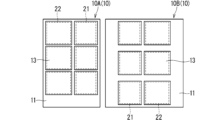
- FIG. 3 is a bottom view of the ceramic substrates 10A and 10B included in the power module 202 according to the first embodiment.
- the back conductor layer 13 is formed in a region corresponding to the portion where the semiconductor elements 21 and 22 are mounted. Specifically, the back conductor layer 13 is formed integrally in an area corresponding to the entire portion where the three sets of semiconductor elements 21 and 22 are mounted, without being divided, and is not formed in other areas. Not yet. Therefore, as shown in FIG. 1, since there is no back conductor layer 13 in the area corresponding to the portion where the wire 41 is directly bonded to the ceramic substrate 10, this area is not bonded to the base portion 70a of the fin base 70.
- the outer dimensions of the back conductor layer 13 of the ceramic substrate 10A are 31 mm x 55 mm, and the outer dimensions of the back conductor layer 13 of the ceramic substrate 10B are 31 mm x 61 mm.
- the area corresponding to the portion of the back conductor layer 13 on which the semiconductor elements 21 and 22 are mounted is the area of the back conductor layer 13 that faces the semiconductor elements 21 and 22 via the base material 11 and the front conductor layer 12. It is.
- FIG. 4 is a bottom view showing another example of the ceramic substrates 10A, 10B included in the power module 202 according to the first embodiment.
- the back conductor layer 13 is divided into regions corresponding to portions on which the semiconductor elements 21 and 22 are each mounted. That is, six back conductor layers 13 are provided for each ceramic substrate 10. This reduces the area of each back conductor layer 13, making it possible to suppress shrinkage cavities that tend to occur when soldering a large area.
- FIG. 5 is a bottom view showing still another example of the ceramic substrates 10A and 10B included in the power module 202 according to the first embodiment.
- the back conductor layer 13 is formed in a region corresponding to a portion where three sets of semiconductor elements 21 and 22 are mounted.
- the four corners of each back conductor layer 13 have an R-chamfered shape. This makes it possible to suppress cracks during temperature cycling, which tend to occur when soldering a large area.
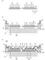
- FIGS. 6(a) to 6(c) are schematic diagrams showing the manufacturing process of the power module 202 according to the first embodiment.
- a sheet-shaped solder 30 having a thickness of 0.2 mm cut into predetermined dimensions is mounted on the surface conductor layer 12 of the ceramic substrate 10, and the semiconductor elements 21 and 22 are mounted on the surface conductor layer 12 of the ceramic substrate 10. Place it in position.
- the semiconductor elements 21 and 22 are soldered to the surface conductor layer 12 by heating the semiconductor elements 21 and 22 arranged on the surface conductor layer 12 in a reflow oven.
- a sheet-like solder 30 with a thickness of 0.4 mm and the ceramic substrate 10 are placed in the area excluding the peripheral edge of the base portion 70a of the fin base 70.
- An adhesive 81 is applied to the peripheral edge of the base portion 70a, and the case 5 is placed thereon.
- the semiconductor elements 21 and 22 and the external electrode 61 are connected by the wire 41, and the signal electrode (not shown) of the semiconductor element 22 and the signal electrode 63 are connected by the wire 42.
- the power module 202 is manufactured by injecting the sealing resin 82 and heating and hardening the sealing resin 82 in an oven.
- the power module 202 includes the semiconductor elements 21 and 22, the ceramic substrate 10 having a mounting surface on which the semiconductor elements 21 and 22 are mounted, and the mounting surface of the ceramic substrate 10 that is opposite to the mounting surface.
- the fin base 70 is bonded to the side surface of the ceramic substrate 10, and the bonding area with the fin base 70 on the ceramic substrate 10 corresponds to the area where the semiconductor elements 21 and 22 are mounted.
- the area of the junction region with 70 is smaller than the area of the portion where semiconductor elements 21 and 22 are mounted.
- the ceramic substrate 10 also includes a back conductor layer 13 forming a surface opposite to the mounting surface, and the back conductor layer 13 is formed in an area corresponding to the portion where the semiconductor elements 21 and 22 are mounted. . Therefore, since the area of the back conductor layer 13 can be reduced, the weight of the power module 202 can be reduced. As described above, it is possible to improve the durability of the power module 202 and reduce energy consumption.
- the area of the front conductor layer 12 of the ceramic substrate 10 is larger than the area of the back conductor layer 13. That is, on the front side of the ceramic substrate 10, the area of the copper conductor layer with a large coefficient of linear expansion is larger than on the back side, but the semiconductor elements 21 and 22, which have a coefficient of linear expansion smaller than that of the front conductor layer 12, By mounting the ceramic substrate 10 on the ceramic substrate 10, it is possible to obtain the effect that the warpage of the ceramic substrate 10 is offset and reduced.
- three sets of semiconductor elements 21 and 22 are mounted on each of the two ceramic substrates 10A and 10B. From the viewpoint of temperature cycle performance and warpage in each ceramic substrate 10, it is considered effective to reduce the external dimensions of the ceramic substrate 10 as much as possible by mounting only one or two semiconductor elements 21, 22 on each ceramic substrate 10.
- the ceramic substrate 10 requires a certain amount of area (frame area) for the base material 11 at the periphery of the ceramic substrate 10, so if the ceramic substrate 10 is divided too much, The frame area of the entire ceramic substrate 10 becomes larger, and the entire power module 202 becomes larger. Therefore, it is considered effective to use two ceramic substrates 10 so that each ceramic substrate 10 has an external dimension that allows three sets of semiconductor elements 21 and 22 to be mounted thereon.
- FIG. 7 is a sectional view of the power module 202 according to the first modification of the first embodiment.
- the fin base 70 is provided with a convex portion 71 that contacts a region of the surface of the ceramic substrate 10 opposite to the mounting surface to which the fin base 70 is not bonded.
- the convex portion 71 is provided at a position in contact with a region of the ceramic substrate 10 where the back conductor layer 13 is not formed.
- the height of the convex portion 71 is 1.0 mm. Since the sealing resin 82 has poor thermal conductivity, the provision of the convex portion 71 reduces the thickness of the sealing resin 82 filled in the gap between the base material 11 and the base portion 70a of the fin base 70. be able to. This makes it easier to radiate Joule heat generated at the joint between the wire 41 and the surface conductor layer 12.
- FIG. 8 is a cross-sectional view of the power module 202 according to the second modification of the first embodiment.
- FIG. 9 is a top view showing a state in which the sealing resin 82 is removed from the power module 202 according to the second modification of the first embodiment.
- FIG. 10 is a bottom view of the ceramic substrate 10A included in the power module 202 according to the second modification of the first embodiment.
- the same components as those described in the first embodiment are given the same reference numerals, and the description thereof will be omitted.
- the power module 202 has a configuration in which three 2-in-1 modules are arranged.
- the power module 202 includes six sets of semiconductor elements 21 and 22, three ceramic substrates 10A, 10B, and 10C, a case 5, a plurality of external electrodes 61, a plurality of signal electrodes 63, and a sealing resin 82.
- a fin base 70 is provided.
- the three ceramic substrates 10A, 10B, and 10C are not distinguished, they are also simply referred to as the ceramic substrate 10.
- Case 5 is different in size from Embodiment 1.
- the case 5 has a width of 70 mm, a depth of 120 mm, and a thickness of 6 mm.
- the fin base 70 is different from the first embodiment in the size of the base portion 70a.
- the size of the base portion 70a is 70 mm in width, 120 mm in depth, and 3 mm in thickness.
- Each of the three ceramic substrates 10 has two surface conductor layers 12 (external dimensions: 41 mm x 32 mm). Two sets of semiconductor elements 21 and 22 are mounted on each of the two surface conductor layers 12 of the three ceramic substrates 10.
- the back conductor layer 13 (external dimensions 32 mm x 32 mm) is formed in a region corresponding to the portion where the semiconductor elements 21 and 22 are mounted. Specifically, the back conductor layer 13 is formed integrally without being divided in an area corresponding to the entire portion where the two sets of semiconductor elements 21 and 22 are mounted, and is not formed in other areas. Not yet. Therefore, as shown in FIG. 10, since there is no back conductor layer 13 in the area corresponding to the portion where the wire 41 is directly bonded to the ceramic substrate 10, this area is not bonded to the base portion 70a of the fin base 70. Therefore, in this region, there is a gap between the base material 11 and the base portion 70a of the fin base 70, and this gap is filled with the sealing resin 82. Note that the configuration of Modification 2 of Embodiment 1 can also be adopted in Modification 1 of Embodiment 1 and Embodiments 2 and 3 below.
- two sets of semiconductor elements 21 and 22 are mounted on each of three ceramic substrates 10A, 10B, and 10C. From the viewpoint of temperature cycle performance and warpage in each ceramic substrate 10, it is considered effective to reduce the external dimensions of the ceramic substrate 10 as much as possible by mounting only one or two semiconductor elements 21, 22 on each ceramic substrate 10.
- the ceramic substrate 10 requires a certain amount of area (frame area) for the base material 11 at the periphery of the ceramic substrate 10, so if the ceramic substrate 10 is divided too much, The frame area of the entire ceramic substrate 10 becomes larger, and the entire power module 202 becomes larger. Therefore, it is considered effective to use three ceramic substrates 10 so that each ceramic substrate 10 has an external dimension that allows two sets of semiconductor elements 21 and 22 to be mounted thereon.
- FIG. 11 is a cross-sectional view of the power module 202 according to the second embodiment.
- FIG. 12 is a bottom view of the ceramic substrate 10 included in the power module 202 according to the second embodiment. Note that, in the second embodiment, the same components as those described in the first embodiment are given the same reference numerals, and a description thereof will be omitted.
- the back conductor layer 13 is provided on the entire back surface of the base material 11. Therefore, a region of the back conductor layer 13 corresponding to the portion where the semiconductor elements 21 and 22 are mounted is bonded to the base portion 70a of the fin base 70, and other regions are not bonded to the fin base 70.
- a solder resist 131 made of UV curing resin is formed for this purpose. The solder resist 131 is soldered to a region of the back conductor layer 13 other than the region corresponding to the portion where the semiconductor elements 21 and 22 are mounted.
- the ceramic substrate 10 includes the back conductor layer 13 forming the surface opposite to the mounting surface, and of the back conductor layer 13, the semiconductor elements 21, A solder resist 131 is formed in an area other than the area where the fin base 22 is mounted to prevent it from being joined to the fin base 70.
- a region of the back conductor layer 13 other than the region corresponding to the portion where the semiconductor elements 21 and 22 are mounted is not joined to the base portion 70a of the fin base 70.
- the convex portion 71 of the modification of the first embodiment may be provided so as to be in contact with a region of the ceramic substrate 10 where the solder resist 131 is formed. Also in this case, it is possible to improve the heat dissipation of Joule heat generated at the joint between the wire 41 and the surface conductor layer 12.
- FIG. 13 is a cross-sectional view of the power module 202 according to the third embodiment.
- FIG. 14 is a bottom view of the ceramic substrate 10 included in the power module 202 according to the third embodiment.
- the same components as those explained in the first and second embodiments are designated by the same reference numerals, and the explanation thereof will be omitted.
- the back conductor layer 13 has a first region 13a which is a region corresponding to the portion where the semiconductor elements 21 and 22 are mounted by the slit 13c and a It is divided into a second region 13b.
- the first region 13a of the back conductor layer 13 is joined to the base portion 70a of the fin base 70, and the second region 13b is not joined to the base portion 70a.
- the ceramic substrate 10 includes the back conductor layer 13 forming the surface opposite to the mounting surface, and the back conductor layer 13 has the slit 13c for the semiconductor element 21. , 22 are mounted, and a second area 13b is the other area.
- the convex portion 71 of the modification of the first embodiment may be provided so as to be in contact with the second region 13b. Also in this case, it is possible to improve the heat dissipation of Joule heat generated at the joint between the wire 41 and the surface conductor layer 12.
- the fin base 70 has been described as being made of aluminum alloy, the same effect can be obtained even if it is made of copper or copper alloy.
- the semiconductor elements 21 and 22 have been described as being made of silicon, similar effects can be obtained even if they are made of wide bandgap semiconductors such as silicon carbide and gallium nitride.
- the solder 30 is composed of 96.5% tin, 3% silver, and 0.5% copper, and its melting point is 217°C, but it is composed of 99.3% tin and 0.7% copper. The same effect can be obtained even if the melting point is 224°C, or if it is composed of 95% tin and 5% antimony and the melting point is 240°C.
- solder 30 The same effect can also be obtained by replacing a part of the solder 30 with a bonding material other than solder, such as a silver epoxy adhesive, a silver sintered material, or a brazing material.
- a bonding material other than solder such as a silver epoxy adhesive, a silver sintered material, or a brazing material.
- wires 41 and 42 have been described as being made of aluminum, the same effect can be obtained even if they are made of aluminum alloy containing a small amount of additives such as iron or copper.
- the external electrode 61 and the signal electrode 63 have been described as frames made of copper, the same effect can be obtained even if they are appropriately nickel-plated, or replaced with ones made of copper alloy or nickel-plated aluminum.
- the sealing resin 82 is made of epoxy resin in which silica filler is dispersed, filler such as alumina may be dispersed in place of the silica filler, or silicone resin may be added to the epoxy resin.
- filler such as alumina may be dispersed in place of the silica filler, or silicone resin may be added to the epoxy resin.
- silicone resin may be added to the epoxy resin.
- the power module 202 according to the first to third embodiments described above is applied to a power conversion device.
- Application of the power module 202 according to Embodiments 1 to 3 is not limited to a specific power conversion device, but hereinafter, as Embodiment 4, the power module 202 according to Embodiments 1 to 3 is applied to a three-phase inverter. A case where module 202 is applied will be explained.
- FIG. 15 is a block diagram showing the configuration of a power conversion system to which the power conversion device according to Embodiment 4 is applied.
- the power conversion system shown in FIG. 15 is composed of a power source 100, a power conversion device 200, and a load 300.
- Power supply 100 is a DC power supply and supplies DC power to power conversion device 200.
- the power source 100 can be composed of various things, for example, it can be composed of a DC system, a solar battery, a storage battery, or it can be composed of a rectifier circuit or an AC/DC converter connected to an AC system. Good too.
- the power supply 100 may be configured with a DC/DC converter that converts DC power output from a DC system into predetermined power.
- the power conversion device 200 is a three-phase inverter connected between the power source 100 and the load 300, converts the DC power supplied from the power source 100 into AC power, and supplies the AC power to the load 300.
- the power conversion device 200 includes a main conversion circuit 201 that converts DC power into AC power and outputs it, and a control circuit 203 that outputs a control signal for controlling the main conversion circuit 201 to the main conversion circuit 201. It is equipped with
- the load 300 is a three-phase electric motor driven by AC power supplied from the power conversion device 200.
- the load 300 is not limited to a specific application, but is a motor installed in various electrical devices, and is used, for example, as a motor for a hybrid vehicle, an electric vehicle, a railway vehicle, an elevator, or an air conditioner.
- the main conversion circuit 201 includes a switching element (not shown) and a freewheeling diode (not shown), and when the switching element switches, it converts DC power supplied from the power supply 100 into AC power, and converts the DC power supplied from the power supply 100 into AC power. Supply to 300.
- the main conversion circuit 201 is a two-level three-phase full bridge circuit, and has six switching elements and each switching element. It can be constructed from six freewheeling diodes arranged in antiparallel.
- At least one of each switching element and each freewheeling diode of main conversion circuit 201 is configured by power module 202 corresponding to any one of the first to third embodiments described above.
- the six switching elements are connected in series every two switching elements to constitute upper and lower arms, and each upper and lower arm constitutes each phase (U phase, V phase, W phase) of the full bridge circuit.
- the output terminals of the upper and lower arms, that is, the three output terminals of the main conversion circuit 201, are connected to the load 300.
- the main conversion circuit 201 includes a drive circuit (not shown) that drives each switching element, but the drive circuit may be built in the power module 202 or a drive circuit may be provided separately from the power module 202.
- the configuration may include the following.
- the drive circuit generates a drive signal for driving the switching element of the main conversion circuit 201 and supplies it to the control electrode of the switching element of the main conversion circuit 201.
- a drive signal that turns the switching element on and a drive signal that turns the switching element off are output to the control electrode of each switching element.
- the drive signal When keeping the switching element in the on state, the drive signal is a voltage signal (on signal) that is greater than or equal to the threshold voltage of the switching element, and when the switching element is kept in the off state, the drive signal is a voltage signal that is less than or equal to the threshold voltage of the switching element. signal (off signal).
- the control circuit 203 controls the switching elements of the main conversion circuit 201 so that the desired power is supplied to the load 300. Specifically, based on the power to be supplied to the load 300, the time (on time) during which each switching element of the main conversion circuit 201 should be in the on state is calculated. For example, the main conversion circuit 201 can be controlled by PWM control that modulates the on-time of the switching element according to the voltage to be output. Then, a control command (control signal) is given to the drive circuit included in the main conversion circuit 201 so that an on signal is output to the switching element that should be in the on state at each time, and an off signal is output to the switching element that should be in the off state. Output.
- the drive circuit outputs an on signal or an off signal as a drive signal to the control electrode of each switching element according to this control signal.
- the power module 202 according to Embodiments 1 to 3 is applied as the switching element and the freewheeling diode of the main conversion circuit 201, so that weight reduction, improved durability, and energy consumption can be achieved. reduction can be achieved.
- the power module 202 according to Embodiments 1 to 3 is applied to a two-level three-phase inverter.
- the present invention is not limited to this and can be applied to various power conversion devices.
- a two-level power converter is used, but a three-level or multi-level power converter may also be used, and in the case of supplying power to a single-phase load, a single-phase inverter is used.
- the power modules 202 according to Nos. 1 to 3 may be applied.
- the power module 202 according to Embodiments 1 to 3 can be applied to a DC/DC converter or an AC/DC converter.
- the power conversion device to which the power module 202 according to Embodiments 1 to 3 is applied is not limited to the case where the above-mentioned load is an electric motor, but is, for example, an electrical discharge machine, a laser processing machine, or an induction heating cooking It can also be used as a power supply device for a device or a non-contact power supply system, and furthermore, it can be used as a power conditioner for a solar power generation system, a power storage system, etc.
- a semiconductor element (Additional note 1) a semiconductor element; an insulating substrate having a mounting surface on which the semiconductor element is mounted; a heat dissipation member bonded to a surface of the insulating substrate opposite to the mounting surface; A bonding region of the insulating substrate with the heat dissipation member is a region corresponding to a portion on which the semiconductor element is mounted, In the power module, an area of a bonding region of the insulating substrate with the heat dissipating member is smaller than an area of a portion on which the semiconductor element is mounted.
- the insulating substrate includes a conductor layer forming a surface opposite to the mounting surface, The power module according to appendix 1, wherein the conductor layer is formed in a region corresponding to a portion where the semiconductor element is mounted.
- the insulating substrate includes a conductor layer forming a surface opposite to the mounting surface,
- the insulating substrate includes a conductor layer forming a surface opposite to the mounting surface, The power module according to appendix 1, wherein the conductor layer is divided by a slit into a region corresponding to a portion where the semiconductor element is mounted and a region other than the region.
- Appendix 7 A main conversion circuit that has the power module described in Appendix 1 and converts and outputs input power; a control circuit that outputs a control signal for controlling the main conversion circuit to the main conversion circuit; A power conversion device equipped with
Landscapes
- Engineering & Computer Science (AREA)
- Power Engineering (AREA)
- Cooling Or The Like Of Semiconductors Or Solid State Devices (AREA)
Priority Applications (3)
| Application Number | Priority Date | Filing Date | Title |
|---|---|---|---|
| JP2024514207A JP7710605B2 (ja) | 2022-04-04 | 2023-03-17 | パワーモジュールおよび電力変換装置 |
| CN202380030904.6A CN118974925A (zh) | 2022-04-04 | 2023-03-17 | 功率模块以及电力转换装置 |
| US18/838,152 US20250149399A1 (en) | 2022-04-04 | 2023-03-17 | Power module and power conversion apparatus |
Applications Claiming Priority (2)
| Application Number | Priority Date | Filing Date | Title |
|---|---|---|---|
| JP2022062224 | 2022-04-04 | ||
| JP2022-062224 | 2022-04-04 |
Publications (1)
| Publication Number | Publication Date |
|---|---|
| WO2023195325A1 true WO2023195325A1 (ja) | 2023-10-12 |
Family
ID=88242723
Family Applications (1)
| Application Number | Title | Priority Date | Filing Date |
|---|---|---|---|
| PCT/JP2023/010614 Ceased WO2023195325A1 (ja) | 2022-04-04 | 2023-03-17 | パワーモジュールおよび電力変換装置 |
Country Status (4)
| Country | Link |
|---|---|
| US (1) | US20250149399A1 (https=) |
| JP (1) | JP7710605B2 (https=) |
| CN (1) | CN118974925A (https=) |
| WO (1) | WO2023195325A1 (https=) |
Cited By (2)
| Publication number | Priority date | Publication date | Assignee | Title |
|---|---|---|---|---|
| EP4661076A1 (en) * | 2024-06-07 | 2025-12-10 | Infineon Technologies AG | Low profile power module |
| WO2026074615A1 (ja) * | 2024-10-01 | 2026-04-09 | 三菱電機株式会社 | 半導体装置および電力変換装置 |
Citations (6)
| Publication number | Priority date | Publication date | Assignee | Title |
|---|---|---|---|---|
| JPH088372A (ja) * | 1994-06-23 | 1996-01-12 | Toshiba Corp | 放熱装置 |
| JP2006344770A (ja) * | 2005-06-09 | 2006-12-21 | Mitsubishi Electric Corp | 半導体モジュールおよび半導体装置 |
| JP2010016254A (ja) * | 2008-07-04 | 2010-01-21 | Toyota Industries Corp | 半導体装置 |
| JP2014096461A (ja) * | 2012-11-08 | 2014-05-22 | Daikin Ind Ltd | パワーモジュール |
| JP2014239084A (ja) * | 2011-09-30 | 2014-12-18 | 三洋電機株式会社 | 回路装置 |
| JP2021034384A (ja) * | 2019-08-13 | 2021-03-01 | 富士電機株式会社 | 半導体装置 |
Family Cites Families (4)
| Publication number | Priority date | Publication date | Assignee | Title |
|---|---|---|---|---|
| JPH0982844A (ja) * | 1995-09-20 | 1997-03-28 | Mitsubishi Electric Corp | 半導体モジュール基板及びその製造方法 |
| JP4969738B2 (ja) * | 2001-06-28 | 2012-07-04 | 株式会社東芝 | セラミックス回路基板およびそれを用いた半導体モジュール |
| JP4621531B2 (ja) * | 2005-04-06 | 2011-01-26 | 株式会社豊田自動織機 | 放熱装置 |
| CN103477428B (zh) * | 2011-05-13 | 2016-10-19 | 富士电机株式会社 | 半导体器件及其制造方法 |
-
2023
- 2023-03-17 JP JP2024514207A patent/JP7710605B2/ja active Active
- 2023-03-17 US US18/838,152 patent/US20250149399A1/en active Pending
- 2023-03-17 CN CN202380030904.6A patent/CN118974925A/zh active Pending
- 2023-03-17 WO PCT/JP2023/010614 patent/WO2023195325A1/ja not_active Ceased
Patent Citations (6)
| Publication number | Priority date | Publication date | Assignee | Title |
|---|---|---|---|---|
| JPH088372A (ja) * | 1994-06-23 | 1996-01-12 | Toshiba Corp | 放熱装置 |
| JP2006344770A (ja) * | 2005-06-09 | 2006-12-21 | Mitsubishi Electric Corp | 半導体モジュールおよび半導体装置 |
| JP2010016254A (ja) * | 2008-07-04 | 2010-01-21 | Toyota Industries Corp | 半導体装置 |
| JP2014239084A (ja) * | 2011-09-30 | 2014-12-18 | 三洋電機株式会社 | 回路装置 |
| JP2014096461A (ja) * | 2012-11-08 | 2014-05-22 | Daikin Ind Ltd | パワーモジュール |
| JP2021034384A (ja) * | 2019-08-13 | 2021-03-01 | 富士電機株式会社 | 半導体装置 |
Cited By (2)
| Publication number | Priority date | Publication date | Assignee | Title |
|---|---|---|---|---|
| EP4661076A1 (en) * | 2024-06-07 | 2025-12-10 | Infineon Technologies AG | Low profile power module |
| WO2026074615A1 (ja) * | 2024-10-01 | 2026-04-09 | 三菱電機株式会社 | 半導体装置および電力変換装置 |
Also Published As
| Publication number | Publication date |
|---|---|
| CN118974925A (zh) | 2024-11-15 |
| US20250149399A1 (en) | 2025-05-08 |
| JP7710605B2 (ja) | 2025-07-18 |
| JPWO2023195325A1 (https=) | 2023-10-12 |
Similar Documents
| Publication | Publication Date | Title |
|---|---|---|
| JP7091878B2 (ja) | パワーモジュール、電力変換装置、及びパワーモジュールの製造方法 | |
| JP7196815B2 (ja) | 半導体モジュール及び電力変換装置 | |
| CN109727960A (zh) | 半导体模块、其制造方法以及电力变换装置 | |
| JP6705393B2 (ja) | 半導体装置及び電力変換装置 | |
| JP7561677B2 (ja) | 電力半導体装置、電力半導体装置の製造方法及び電力変換装置 | |
| JP6743728B2 (ja) | 半導体パワーモジュール及び電力変換装置 | |
| JP7710605B2 (ja) | パワーモジュールおよび電力変換装置 | |
| CN111052325B (zh) | 半导体模块以及电力转换装置 | |
| JPWO2020174584A1 (ja) | 半導体装置、半導体装置の製造方法および電力変換装置 | |
| US10777499B2 (en) | Semiconductor module, method for manufacturing the same and power conversion apparatus | |
| KR20140130862A (ko) | 파워모듈 제조방법 및 이를 통해 재조된 고방열 파워모듈 | |
| JP7584668B2 (ja) | パワーモジュールおよび電力変換装置 | |
| JP7638193B2 (ja) | 半導体装置および電力変換装置 | |
| US11652032B2 (en) | Semiconductor device having inner lead exposed from sealing resin, semiconductor device manufacturing method thereof, and power converter including the semiconductor device | |
| JP2024010348A (ja) | 半導体モジュールおよび電力変換装置 | |
| JP7630721B2 (ja) | 半導体モジュール、電力変換装置、および半導体モジュールの製造方法 | |
| JP2023169589A (ja) | パワーモジュールおよび電力変換装置 | |
| JP7854857B2 (ja) | 半導体モジュールの製造方法、電力変換装置の製造方法、半導体モジュール、電力変換装置 | |
| JP7686143B2 (ja) | 半導体装置、電力変換装置および半導体装置の製造方法 | |
| JP7715022B2 (ja) | 半導体装置及び電力変換装置 | |
| JP2026046734A (ja) | パワーモジュールおよび電力変換装置 | |
| JP2023110389A (ja) | 半導体装置、電力変換装置、および、半導体装置の製造方法 | |
| CN111448653A (zh) | 半导体装置及电力转换装置 | |
| JP2024139935A (ja) | 半導体装置および電力変換装置 | |
| JP2025041092A (ja) | パワーモジュールおよび電力変換装置 |
Legal Events
| Date | Code | Title | Description |
|---|---|---|---|
| 121 | Ep: the epo has been informed by wipo that ep was designated in this application |
Ref document number: 23784615 Country of ref document: EP Kind code of ref document: A1 |
|
| ENP | Entry into the national phase |
Ref document number: 2024514207 Country of ref document: JP Kind code of ref document: A |
|
| WWE | Wipo information: entry into national phase |
Ref document number: 18838152 Country of ref document: US |
|
| WWE | Wipo information: entry into national phase |
Ref document number: 202380030904.6 Country of ref document: CN |
|
| NENP | Non-entry into the national phase |
Ref country code: DE |
|
| 122 | Ep: pct application non-entry in european phase |
Ref document number: 23784615 Country of ref document: EP Kind code of ref document: A1 |
|
| WWP | Wipo information: published in national office |
Ref document number: 18838152 Country of ref document: US |