WO2023175661A1 - 診断装置、半導体製造装置システム、半導体装置製造システムおよび診断方法 - Google Patents
診断装置、半導体製造装置システム、半導体装置製造システムおよび診断方法 Download PDFInfo
- Publication number
- WO2023175661A1 WO2023175661A1 PCT/JP2022/011254 JP2022011254W WO2023175661A1 WO 2023175661 A1 WO2023175661 A1 WO 2023175661A1 JP 2022011254 W JP2022011254 W JP 2022011254W WO 2023175661 A1 WO2023175661 A1 WO 2023175661A1
- Authority
- WO
- WIPO (PCT)
- Prior art keywords
- temperature data
- diagnostic device
- change
- sample
- abnormality
- Prior art date
- Legal status (The legal status is an assumption and is not a legal conclusion. Google has not performed a legal analysis and makes no representation as to the accuracy of the status listed.)
- Ceased
Links
Images




Classifications
-
- H—ELECTRICITY
- H10—SEMICONDUCTOR DEVICES; ELECTRIC SOLID-STATE DEVICES NOT OTHERWISE PROVIDED FOR
- H10P—GENERIC PROCESSES OR APPARATUS FOR THE MANUFACTURE OR TREATMENT OF DEVICES COVERED BY CLASS H10
- H10P72/00—Handling or holding of wafers, substrates or devices during manufacture or treatment thereof
- H10P72/70—Handling or holding of wafers, substrates or devices during manufacture or treatment thereof for supporting or gripping
- H10P72/72—Handling or holding of wafers, substrates or devices during manufacture or treatment thereof for supporting or gripping using electrostatic chucks
- H10P72/722—Details of electrostatic chucks
-
- G—PHYSICS
- G01—MEASURING; TESTING
- G01N—INVESTIGATING OR ANALYSING MATERIALS BY DETERMINING THEIR CHEMICAL OR PHYSICAL PROPERTIES
- G01N25/00—Investigating or analyzing materials by the use of thermal means
- G01N25/18—Investigating or analyzing materials by the use of thermal means by investigating thermal conductivity
-
- G—PHYSICS
- G01—MEASURING; TESTING
- G01N—INVESTIGATING OR ANALYSING MATERIALS BY DETERMINING THEIR CHEMICAL OR PHYSICAL PROPERTIES
- G01N25/00—Investigating or analyzing materials by the use of thermal means
- G01N25/72—Investigating presence of flaws
-
- H—ELECTRICITY
- H10—SEMICONDUCTOR DEVICES; ELECTRIC SOLID-STATE DEVICES NOT OTHERWISE PROVIDED FOR
- H10P—GENERIC PROCESSES OR APPARATUS FOR THE MANUFACTURE OR TREATMENT OF DEVICES COVERED BY CLASS H10
- H10P72/00—Handling or holding of wafers, substrates or devices during manufacture or treatment thereof
- H10P72/06—Apparatus for monitoring, sorting, marking, testing or measuring
- H10P72/0602—Temperature monitoring
-
- H—ELECTRICITY
- H10—SEMICONDUCTOR DEVICES; ELECTRIC SOLID-STATE DEVICES NOT OTHERWISE PROVIDED FOR
- H10P—GENERIC PROCESSES OR APPARATUS FOR THE MANUFACTURE OR TREATMENT OF DEVICES COVERED BY CLASS H10
- H10P72/00—Handling or holding of wafers, substrates or devices during manufacture or treatment thereof
- H10P72/06—Apparatus for monitoring, sorting, marking, testing or measuring
- H10P72/0604—Process monitoring, e.g. flow or thickness monitoring
-
- H—ELECTRICITY
- H10—SEMICONDUCTOR DEVICES; ELECTRIC SOLID-STATE DEVICES NOT OTHERWISE PROVIDED FOR
- H10P—GENERIC PROCESSES OR APPARATUS FOR THE MANUFACTURE OR TREATMENT OF DEVICES COVERED BY CLASS H10
- H10P72/00—Handling or holding of wafers, substrates or devices during manufacture or treatment thereof
- H10P72/06—Apparatus for monitoring, sorting, marking, testing or measuring
- H10P72/0616—Monitoring of warpages, curvatures, damages, defects or the like
-
- H—ELECTRICITY
- H10—SEMICONDUCTOR DEVICES; ELECTRIC SOLID-STATE DEVICES NOT OTHERWISE PROVIDED FOR
- H10P—GENERIC PROCESSES OR APPARATUS FOR THE MANUFACTURE OR TREATMENT OF DEVICES COVERED BY CLASS H10
- H10P72/00—Handling or holding of wafers, substrates or devices during manufacture or treatment thereof
- H10P72/70—Handling or holding of wafers, substrates or devices during manufacture or treatment thereof for supporting or gripping
-
- H—ELECTRICITY
- H10—SEMICONDUCTOR DEVICES; ELECTRIC SOLID-STATE DEVICES NOT OTHERWISE PROVIDED FOR
- H10P—GENERIC PROCESSES OR APPARATUS FOR THE MANUFACTURE OR TREATMENT OF DEVICES COVERED BY CLASS H10
- H10P72/00—Handling or holding of wafers, substrates or devices during manufacture or treatment thereof
- H10P72/70—Handling or holding of wafers, substrates or devices during manufacture or treatment thereof for supporting or gripping
- H10P72/72—Handling or holding of wafers, substrates or devices during manufacture or treatment thereof for supporting or gripping using electrostatic chucks
-
- H—ELECTRICITY
- H01—ELECTRIC ELEMENTS
- H01J—ELECTRIC DISCHARGE TUBES OR DISCHARGE LAMPS
- H01J37/00—Discharge tubes with provision for introducing objects or material to be exposed to the discharge, e.g. for the purpose of examination or processing thereof
- H01J37/32—Gas-filled discharge tubes
- H01J37/32917—Plasma diagnostics
- H01J37/32935—Monitoring and controlling tubes by information coming from the object and/or discharge
Definitions
- the present disclosure relates to a diagnostic device, a semiconductor manufacturing equipment system, a semiconductor device manufacturing system, and a diagnostic method.
- the present invention relates to a diagnostic device (PHM: Prognostics and Health Management) that uses time-series signals (sensor waveform data) sequentially acquired from multiple sensors of a plasma processing device, which is a semiconductor manufacturing device that processes semiconductor wafers.
- PPM Prognostics and Health Management
- the surface condition of an electrostatic chuck (ESC) that mounts and adsorbs a wafer during plasma processing gradually deteriorates due to surface damage, deposits, and other causes.
- ESC electrostatic chuck
- an abnormality in the wafer processing speed or an abnormality in wafer suction occurs, so it is desirable to have a technique that detects changes in the surface condition of the ESC and performs maintenance before the abnormality occurs.
- real-time monitoring of the surface condition of the ESC of the operating device is difficult due to the lack of associated sensors.
- An abnormality in the surface condition of the ESC is detected by a change in the thermal conductivity of the ESC surface.
- a method has been proposed in which a change in thermal conductivity is detected by a change in temperature sensor data, such as the method described in Patent Document 1.
- the value of the temperature sensor is kept constant by the temperature control system, so this method cannot detect changes in the thermal conductivity of the surface of the ESC.
- an object of the present disclosure is to provide a technique for detecting an abnormality in the surface state of a film of an electrostatic chuck.
- a diagnostic device for diagnosing the state of semiconductor manufacturing equipment that includes a sample stage on which a sample electrostatically adsorbed to a film is placed, temperature data before and after changes in energy applied to the sample are provided. is acquired, and an abnormality in the membrane is detected based on the acquired temperature data.
- the diagnostic device capable of predicting an abnormality changes the energy input to the wafer in the plasma control unit, acquires temperature change data before and after the energy change from the temperature sensor in the data collection unit, and The amount of change or rate of change of the temperature change data is calculated as a feature amount, and the abnormality detection section determines that the surface condition of the electrostatic chuck is abnormal when the feature amount exceeds a threshold value.
- FIG. 1 is a diagram illustrating an example of the configuration of a failure diagnosis device according to a first embodiment
- FIG. 2 is a diagram showing an example of an electrode configuration of the etching apparatus shown in FIG. 1.
- FIG. 3 is a diagram showing an example of sensor data according to Example 1.
- FIG. 3 is a diagram illustrating an example of a processing flow of feature amount calculation and abnormality determination according to the first embodiment. It is a figure which shows the calculation example of the feature-value F1, F2, F3. It is a figure which shows the calculation example of the feature-value F4.
- 5 is a diagram showing an example of abnormality determination according to the first embodiment.
- FIG. 7 is a diagram illustrating an example of a wafer chucking operation according to a second embodiment.
- FIG. FIG. 3 is a diagram showing an example of a diagnosis result display according to the first embodiment.
- An embodiment of the present invention is a diagnostic device for a plasma processing apparatus.
- the diagnostic device may be a general personal computer equipped with a processor and memory, and may be an implementation of software that processes according to a program, or a diagnostic device may be a dedicated hardware rather than a general computer. It may also be an implementation of software.
- diagnostic device may be externally connected, or may be externally connected as a module that is also used for other data processing.
- a semiconductor manufacturing equipment system 10 shown in FIG. 1 includes a failure diagnosis device (FDE, sometimes simply referred to as a diagnosis device) 100 and an etching device (PEE) 200.
- the failure diagnosis device 100 and the etching device 200 are connected by a network line NW.
- the etching apparatus 200 is a plasma processing apparatus as a semiconductor manufacturing apparatus.
- the fault diagnosis device (FDE) 100 includes a data collection unit (DCD) 101, a feature quantity calculation unit (FCP) 102, and an abnormality detection unit (ADD) 103, and is connected to the etching apparatus 200 by a network line NW.
- the etching apparatus 200 includes a plasma control unit (PCD) 201 and a chamber (CHA) 202 that are related to the present invention.
- the failure diagnosis device 100 receives time-series data (hereinafter referred to as sensor data) 204 measured by a sensor during the treatment process from the etching device 200 via the network line NW, analyzes the received sensor data 204, Output the analysis result RS.
- sensor data time-series data
- the plasma control unit 201 controls the energy applied to the wafer 203 as a sample in the chamber 202.
- the wafer 203 is processed under set process conditions, and sensor data 204 of this process is transmitted to the data collection unit 101 in real time.
- the data collection unit 101 extracts energy and temperature sensor data from the received sensor data 204 and transmits it to the feature calculation unit 102 .
- the feature amount calculation unit 102 acquires temperature change data before and after the energy change from the sensor data 204, and calculates the amount of change in the temperature change data or the rate of change in the temperature change data as a feature amount.
- the abnormality detection unit 103 analyzes the temporal change of the calculated feature amount, and outputs an analysis result RS indicating whether or not there is an abnormality.
- FIG. 2 shows an example of the configuration of the chamber 202.
- a sample stage is provided that includes an electrostatic chuck (ESC) 205 on which a wafer 203 is mounted and electrostatically attracted during plasma processing.
- the wafer 203 electrostatically attracted to the film 210 constituting the ESC 205 is placed on the sample stage.
- the temperature of the ESC 205 is controlled according to the process setting conditions, the wafer 203 is moved onto the ESC 205, and plasma PLA is generated in the space above the wafer 203.
- the present invention detects abnormalities in the surface state of the film 210 of the ESC 205 by monitoring changes in the thermal conductivity THC. The purpose is to detect.
- the temperature of the ESC 205 is controlled by a feedback temperature control system using a plurality of heaters 206 and a temperature sensor 207.
- the feedback temperature control system controls the heater power to be decreased when the temperature of the temperature sensor 207 is higher than the temperature of the set condition, and to increase the heater power when the temperature of the temperature sensor 207 is lower than the temperature of the set condition. Therefore, the sensor value (detected temperature value) of the temperature sensor 207 becomes almost constant during the process.
- the sensor value of the temperature sensor 207 changes temporarily, but since the temperature control by the feedback temperature control system operates, the temperature of the temperature sensor 207 returns to the temperature of the set condition.
- Temperature change data can be obtained from the above phenomenon, and the change in the thermal conductivity THC can be estimated using the temperature change data.
- the amount of energy (plasma heat input) 209 input from the plasma PLA to the wafer 203 changes, and the sensor value of the temperature sensor 207 temporarily deviates from the set condition value and returns.
- the rate of temperature change is calculated from the temperature change data of this process, and if the rate is faster than usual, it can be seen that the thermal conductivity THC has increased.
- FIG. 3 shows an example of the above sensor data.
- FIG. 3A is an example of sensor data showing temporal changes in plasma power of plasma PLA, where the vertical axis is plasma power and the horizontal axis is time (TT).
- FIG. 3B is an example of sensor data showing a change over time in the temperature sensor value (Sensor Temperature 01) of the temperature sensor 207, where the vertical axis is the temperature sensor value and the horizontal axis is time (TT).
- FIG. 3(c) is a table showing an example of sensor data collected at intervals of 0.1 seconds.
- the timestamp is at an interval of 0.1 seconds
- the sensor data is, in this example, the power of the plasma PLA (Plasma Power), the temperature sensor value (Sensor Temperature 01), and the power of the heater 206 (Heater Power 01). etc. are shown as examples.
- the plasma power of the plasma PLA is set to decrease once and then increase.
- the temperature sensor value (Sensor Temperature 01) decreases and increases.
- the temperature sensor value of the temperature sensor 207 increases and decreases.
- Sensor data is collected at intervals of 0.1 seconds, and is stored and transmitted as shown in the table in FIG. 3(c).
- FIG. 4 is a diagram illustrating an example of a processing flow of feature amount calculation and abnormality determination according to the embodiment.
- the processing flow in FIG. 4 is a processing flow executed by an application in a semiconductor device manufacturing system including a platform on which an application for diagnosing the state of semiconductor manufacturing equipment is installed.
- Step S40 First, in a semiconductor manufacturing apparatus 200 equipped with a sample stage on which a sample (wafer) 203 electrostatically attracted to the membrane 210 of the ESC 205 is placed, the energy input to the wafer 203 is changed by controlling plasma power. .
- the part of the plasma power change in the original process conditions can be used, but a process condition dedicated to failure diagnosis may be added to the original process conditions.
- Step S41 sensor data (T) before and after the energy change performed in step S40 (before and after the energy change) is collected.
- sensor data (T) is collected in a time range of 20 seconds from 5 seconds before the energy change to 20 seconds after the energy change. That is, in a diagnostic apparatus 100 that diagnoses the state of a semiconductor manufacturing apparatus 200 that includes a sample stage on which a sample 203 electrostatically attracted to a membrane 210 of an ESC 205 is placed, a sensor before and after a change in energy applied to a sample 203 is used. Data (hereinafter also referred to as temperature data) T is acquired. Then, based on the acquired temperature data T, the diagnostic device 100 detects an abnormality in the membrane 210 of the ESC 205.
- Step S42 From here on, the feature amount F1 is calculated using the data T.
- Data T1 before energy change is extracted. For example, the first 10 pieces of data T are taken as data (T1).
- Data T2 after the energy change is extracted.
- the last 10 pieces of data T are taken as data (T2).
- average values MEAN(T1), MEAN(T2) are calculated for each of the data before the energy change (T1) and the data after the energy change (T2).
- Step S43 Then, the feature amount F1 is calculated using Equation 1.
- F1 MEAN(T1)-MEAN(T2)
- feature amount F1 The difference between the T1 average value and the T2 average value (feature amount F1) is calculated using Equation 1. That is, the difference between the average value of the temperature data (T1) before the energy change and the average value of the temperature data (T2) after the energy change is determined as the feature amount F1.
- Step S44 Next, the maximum value (TMAX) and minimum value (TMIN) of data T are obtained.
- Step S45 Then, the feature amount F2 is calculated using Equation 2.
- F2 TMAX-TMIN Formula 2
- feature amount F2 The difference between the maximum value and the minimum value of the temperature data T (feature amount F2) is calculated by Equation 2. That is, the difference between the maximum value and the minimum value of the temperature data T is determined as the feature amount F2.
- Step S46 Next, the time (L1) of the maximum value (TMAX) of data T and the time (L2) of the minimum value (TMIN) of data T are acquired.
- Step S47 The slope of data T with respect to time between time L1 and time L2 is calculated as feature amount F3. That is, using data between the maximum value (TMAX) of the temperature data T and the minimum value (TMIN) of the temperature data T, the slope with respect to time (L1, L2) is determined as the feature amount F3.
- Step S48 Before this processing, normal waveform data of data T is prepared. This normal waveform data is past data T extracted from sensor data of past normal processing processes under the same calculation conditions.
- the feature amount F4 is calculated using Equation 3.
- Equation 3 the difference (feature amount F4) between the temperature data T and predefined normal waveform data is calculated. That is, the difference between the normal waveform data of the predefined normal temperature data and the waveform data of the temperature data T is obtained as the feature amount F4.
- Step S49 The above calculation completes the calculation of the feature amounts F1, F2, F3, and F4. Changes in the feature values (F1, F2, F3, F4) over time are monitored, and when they exceed a predetermined threshold value, it is determined to be abnormal. At the time of calculation, a general statistical processing method may be added to the feature value calculation method for the purpose of noise reduction or the like. Further, when a plurality of local maximum values and local minimum values can be taken instead of the maximum value and minimum value, depending on the pattern of plasma power change, the number of feature amounts may be increased.
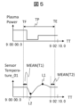
- FIG. 5 shows an example of the feature amounts F1, F2, and F3.
- the data T is data of the period TP before and after the energy change from 5 seconds before the time TF of the first energy change to 20 seconds after the time TE of the last energy change.
- the feature amount F1 can be calculated by calculating the T1 average (MEAN(T1)) using the first 10 pieces of data T, and calculating the T2 average (MEAN(T2)) using the last 10 pieces of data. Then, the feature quantity F2 and the feature quantity F3 can be calculated using the maximum value L1 and the minimum value L2 of the data T, and the data T between the maximum value L1 and the minimum value L2.
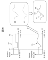
- FIG. 6 shows an example of the feature amount F4.
- Data T (61) is acquired using the same method as in the example of FIG. Then, the feature amount F4, which is the difference between the normal waveform data 60 and the data T(61), can be calculated.
- FIG. 7 is a diagram showing an example of abnormality determination.
- (a) of FIG. 7 is an example of monitoring the change in the feature amount F1 over time, where the vertical axis is the value of the feature amount F1, and the horizontal axis is the cumulative time CT of the etching process (or the number of processed wafers N): Indicates CT (or N).
- FIG. 7(b) is an example of monitoring the change in the feature amount F2 over time, where the vertical axis represents the value of the feature amount F2, and the horizontal axis represents the cumulative time CT of the etching process (or the number of processed wafers N). show.
- FIG. 7 is a diagram showing an example of abnormality determination.
- FIG. 7(c) is an example of monitoring the change in the feature amount F3 over time, where the vertical axis represents the value of the feature amount F3, and the horizontal axis represents the cumulative time CT of the etching process (or the number of processed wafers N). show.
- FIG. 7(d) is an example of monitoring the change in the feature amount F4 over time, where the vertical axis represents the value of the feature amount F4, and the horizontal axis represents the cumulative time CT of the etching process (or the number of processed wafers N). show.
- abnormalities are determined by analyzing the time series of feature amounts. For example, there are two upper and lower thresholds TH1 and TH2 for the feature amount F3, and if the value of the feature amount F3 exceeds either threshold TH1 or TH2, it is determined that the feature amount F3 is abnormal. In other words, if the feature amount F3 exceeds the range between the thresholds TH1 and TH2, it is determined that the feature amount F3 is abnormal (in other words, if it goes out of the range between TH1 and TH2 (F3>TH1 or TH2>F3) case), the feature amount F3 is determined to be abnormal).
- the feature amount F4 is determined to be abnormal (that is, if F4>TH3, the feature amount F4 is determined to be abnormal).
- the feature amount F1, F2, F3, and F4 becomes abnormal, it is determined that an abnormality has occurred in the apparatus. However, it may be determined that an abnormality has occurred in the etching apparatus 200 when there is an abnormality in two or more feature amounts, taking into consideration the relationship between the feature amounts and the failure.
- FIG. 7E shows an ESC 205 having four zones (first zone Z1, second zone Z2, third zone Z3, and fourth zone Z4).
- the processing flow for calculating the feature quantities (F1-F4) and determining an abnormality in FIG. 4 shows, for example, the processing flow for calculating the feature quantities (F1-F4) and determining an abnormality for the first zone Z1 of the ESC 205.
- the feature values (F1-F4) of each zone Z1, Z2, Z3, and Z4 are ) can be calculated and abnormality judgment can be made.
- a diagnostic method for diagnosing the state of the semiconductor manufacturing apparatus 200 that includes a sample stage on which the sample 203 electrostatically attracted to the film 210 is placed acquires temperature data before and after changes in the energy applied to the sample 203. and a step of detecting an abnormality in the membrane 210 based on the acquired temperature data.
- the semiconductor manufacturing equipment system 10 in FIG. 1 can be rephrased as a semiconductor device manufacturing system.
- the semiconductor device manufacturing system diagnoses the state of the semiconductor manufacturing device 200, which is connected to the semiconductor manufacturing device 200 via the network NW and includes a sample stage on which the sample 203 electrostatically attracted to the film 210 is placed. Equipped with a platform on which applications are implemented. Then, the application executes a step of acquiring temperature data before and after a change in the energy applied to the sample 203, and a step of detecting an abnormality in the membrane 210 based on the acquired temperature data. It is configured.
- a list of feature values, calculation results, abnormality diagnosis results, etc. can be displayed on a GUI (Graphic User Interface).
- the diagnostic device 100 has a display screen that displays a list of feature values, calculation results, abnormality diagnosis results, etc. using a GUI (Graphic User Interface).
- the list of feature values, calculation results, abnormality diagnosis results, etc. are displayed on the server using a GUI (Graphic User Interface).
- a display screen may be provided to display the information.
- FIG. 9 shows an example of the GUI screen.
- a GUI screen 90 in FIG. 9 depicts an example of an ESC fault diagnostic screen.
- an anomaly judgment area 95 changes over time of each calculated feature quantity (F1-F4) are displayed.
- the feature amount (in this example, F4) indicating the abnormality is presented in the alarm area 96.
- Action 97 presents tasks such as maintenance implementation and process condition adjustment as countermeasures for the abnormality.
- the feature values (F1, F2, F3, F4) which are the amount of change in temperature data or the speed of change in temperature data, the changes over time in the feature values (F1, F2, F3, F4), or the presence or absence of an abnormality in the membrane 210 are This is displayed on the GUI screen 90, and if the membrane 210 is abnormal, an action to be taken when the membrane 210 is abnormal is presented on the GUI screen 90.
- a technique for detecting an abnormality in the surface state of the film 210 of the electrostatic chuck 205 can be provided. This improves the accuracy of detecting abnormalities in the surface state of the film 210 of the electrostatic chuck 205.
- Example 2 a process will be described in which the wafer chuck 80 (the wafer 203 is placed on the ESC 205) is used instead of plasma heat input.
- the parts that are not explained are the same as in the first embodiment. That is, redundant explanation of the same parts as in the first embodiment will be omitted.
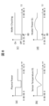
- FIGS. 8A and 8B show the situation of Example 1 (same as FIGS. 3A and 3B), and FIGS. 8C and 8D show the wafer chuck 80.
- FIGS. 8C and 8D show the wafer chuck 80.
- (c) of FIG. 8 shows the change between the on state (On) and the off state (Off) of the wafer chuck 80, and the vertical axis shows the on state (On) and the off state (Off) of the wafer chuck 80, The horizontal axis indicates time TT.
- (d) of FIG. 8 shows the state of the heater power value (data P) which is the amount of power consumed by the heater 206, the vertical axis shows the state of the heater power value (data P), and the horizontal axis shows the time TT. show.
- the temperature sensor value (data T) used in the feature value calculation in the first embodiment is changed to the heater power value (data P), which is the amount of power consumed by the heater, in the second embodiment.
- the temperature sensor value and heater power value are kept constant by temperature control. Since the temperature of the wafer 203 is lower than that of the ESC 205 during the wafer chuck 80, the temperature of the ESC 205 becomes lower.
- the temperature control system detects the temperature change of ESC 205 and increases the heater power of heater 206. When the temperature of the wafer 203 becomes the same as the temperature of the ESC 205, the heater power value of the heater 206 gradually returns to its original value.
- feature amounts can be calculated in the same manner as in the first embodiment, and an abnormality can be determined.
- Example 2 the power consumption of the heater 206 is acquired instead of the temperature data before and after the change in the energy applied to the sample 203, and the film 210 is An abnormality is detected.
- the temperature data of the ESC 205 before and after the electrostatic adsorption of the sample 203 is acquired, and the obtained temperature data of the ESC 205 before and after the electrostatic adsorption of the sample 203 is obtained. It may be configured such that an abnormality in the membrane 203 is detected based on temperature data.
Landscapes
- General Health & Medical Sciences (AREA)
- General Physics & Mathematics (AREA)
- Life Sciences & Earth Sciences (AREA)
- Chemical & Material Sciences (AREA)
- Analytical Chemistry (AREA)
- Biochemistry (AREA)
- Health & Medical Sciences (AREA)
- Immunology (AREA)
- Physics & Mathematics (AREA)
- Pathology (AREA)
- Drying Of Semiconductors (AREA)
- Container, Conveyance, Adherence, Positioning, Of Wafer (AREA)
- Investigating Or Analyzing Materials Using Thermal Means (AREA)
- Testing Of Individual Semiconductor Devices (AREA)
- Testing Or Measuring Of Semiconductors Or The Like (AREA)
Priority Applications (9)
| Application Number | Priority Date | Filing Date | Title |
|---|---|---|---|
| US18/026,217 US20240321608A1 (en) | 2022-03-14 | 2022-03-14 | Diagnostic device, semiconductor manufacturing equipment system, semiconductor equipment manufacturing system, and diagnostic method |
| CN202280005629.8A CN117063065A (zh) | 2022-03-14 | 2022-03-14 | 诊断装置、半导体制造装置系统、半导体装置制造系统以及诊断方法 |
| JP2023512208A JP7471513B2 (ja) | 2022-03-14 | 2022-03-14 | 診断装置、半導体製造装置システム、半導体装置製造システムおよび診断方法 |
| PCT/JP2022/011254 WO2023175661A1 (ja) | 2022-03-14 | 2022-03-14 | 診断装置、半導体製造装置システム、半導体装置製造システムおよび診断方法 |
| KR1020237005515A KR20230135558A (ko) | 2022-03-14 | 2022-03-14 | 진단 장치, 반도체 제조 장치 시스템, 반도체 장치 제조 시스템 및 진단 방법 |
| TW113119789A TW202436868A (zh) | 2022-03-14 | 2023-02-22 | 診斷裝置、半導體製造裝置系統、半導體裝置製造系統及診斷方法 |
| TW112106470A TWI849766B (zh) | 2022-03-14 | 2023-02-22 | 診斷裝置、半導體製造裝置系統、半導體裝置製造系統及診斷方法 |
| JP2024062447A JP7796794B2 (ja) | 2022-03-14 | 2024-04-09 | 診断装置、半導体装置製造システムおよび診断方法 |
| JP2025108667A JP2025126302A (ja) | 2022-03-14 | 2025-06-27 | 診断装置、半導体製造装置システム、半導体装置製造システムおよび診断方法 |
Applications Claiming Priority (1)
| Application Number | Priority Date | Filing Date | Title |
|---|---|---|---|
| PCT/JP2022/011254 WO2023175661A1 (ja) | 2022-03-14 | 2022-03-14 | 診断装置、半導体製造装置システム、半導体装置製造システムおよび診断方法 |
Publications (1)
| Publication Number | Publication Date |
|---|---|
| WO2023175661A1 true WO2023175661A1 (ja) | 2023-09-21 |
Family
ID=88022812
Family Applications (1)
| Application Number | Title | Priority Date | Filing Date |
|---|---|---|---|
| PCT/JP2022/011254 Ceased WO2023175661A1 (ja) | 2022-03-14 | 2022-03-14 | 診断装置、半導体製造装置システム、半導体装置製造システムおよび診断方法 |
Country Status (6)
| Country | Link |
|---|---|
| US (1) | US20240321608A1 (https=) |
| JP (3) | JP7471513B2 (https=) |
| KR (1) | KR20230135558A (https=) |
| CN (1) | CN117063065A (https=) |
| TW (2) | TWI849766B (https=) |
| WO (1) | WO2023175661A1 (https=) |
Citations (3)
| Publication number | Priority date | Publication date | Assignee | Title |
|---|---|---|---|---|
| US20100045316A1 (en) * | 2008-02-29 | 2010-02-25 | Lam Research Corporation | Method for inspecting electrostatic chucks with kelvin probe analysis |
| US20180047607A1 (en) * | 2014-02-12 | 2018-02-15 | Applied Materials, Inc. | Apparatus and method for measurement of the thermal performance of an electrostatic wafer chuck |
| WO2021255784A1 (ja) * | 2020-06-15 | 2021-12-23 | 株式会社日立ハイテク | 装置診断装置、装置診断方法、プラズマ処理装置および半導体装置製造システム |
Family Cites Families (13)
| Publication number | Priority date | Publication date | Assignee | Title |
|---|---|---|---|---|
| JPH08141861A (ja) * | 1994-11-14 | 1996-06-04 | Fujitsu Ltd | 真空チャック装置 |
| JP3556549B2 (ja) * | 1999-12-10 | 2004-08-18 | シャープ株式会社 | シート抵抗測定器および電子部品製造方法 |
| JP3897344B2 (ja) * | 2002-08-23 | 2007-03-22 | 株式会社オングストロームテクノロジーズ | チャッキング状態検出方法及びプラズマ処理装置 |
| WO2010026893A1 (ja) * | 2008-09-04 | 2010-03-11 | 株式会社クリエイティブ テクノロジー | 静電チャック装置及び基板の吸着状態判別方法 |
| CN103779165B (zh) * | 2012-10-19 | 2016-08-31 | 北京北方微电子基地设备工艺研究中心有限责任公司 | 等离子体设备及工件位置检测方法 |
| JP6222656B2 (ja) * | 2013-07-25 | 2017-11-01 | 株式会社クリエイティブテクノロジー | センサ一体型吸着チャック及び処理装置 |
| JP6418791B2 (ja) | 2014-05-29 | 2018-11-07 | 株式会社日立製作所 | 冷却装置の異常検知システム |
| KR101809654B1 (ko) * | 2014-06-03 | 2017-12-18 | 에이피시스템 주식회사 | 기판 처리 장치 및 그 작동 방법 |
| JP6316703B2 (ja) * | 2014-08-19 | 2018-04-25 | 東京エレクトロン株式会社 | 基板処理装置および基板処理方法 |
| KR102581356B1 (ko) * | 2016-08-30 | 2023-09-21 | 삼성전자주식회사 | 기판 처리 장치의 이상 진단 방법 및 이를 수행하기 위한 장치 |
| SG11202001500VA (en) * | 2017-08-22 | 2020-03-30 | Shinkawa Kk | Mounting apparatus and temperature measurement method |
| CN111699544B (zh) * | 2018-02-14 | 2024-03-22 | 东京毅力科创株式会社 | 基板处理装置、基板处理方法以及存储介质 |
| JP7137943B2 (ja) * | 2018-03-20 | 2022-09-15 | 株式会社日立ハイテク | 探索装置、探索方法及びプラズマ処理装置 |
-
2022
- 2022-03-14 KR KR1020237005515A patent/KR20230135558A/ko not_active Ceased
- 2022-03-14 JP JP2023512208A patent/JP7471513B2/ja active Active
- 2022-03-14 WO PCT/JP2022/011254 patent/WO2023175661A1/ja not_active Ceased
- 2022-03-14 CN CN202280005629.8A patent/CN117063065A/zh active Pending
- 2022-03-14 US US18/026,217 patent/US20240321608A1/en active Pending
-
2023
- 2023-02-22 TW TW112106470A patent/TWI849766B/zh active
- 2023-02-22 TW TW113119789A patent/TW202436868A/zh unknown
-
2024
- 2024-04-09 JP JP2024062447A patent/JP7796794B2/ja active Active
-
2025
- 2025-06-27 JP JP2025108667A patent/JP2025126302A/ja active Pending
Patent Citations (3)
| Publication number | Priority date | Publication date | Assignee | Title |
|---|---|---|---|---|
| US20100045316A1 (en) * | 2008-02-29 | 2010-02-25 | Lam Research Corporation | Method for inspecting electrostatic chucks with kelvin probe analysis |
| US20180047607A1 (en) * | 2014-02-12 | 2018-02-15 | Applied Materials, Inc. | Apparatus and method for measurement of the thermal performance of an electrostatic wafer chuck |
| WO2021255784A1 (ja) * | 2020-06-15 | 2021-12-23 | 株式会社日立ハイテク | 装置診断装置、装置診断方法、プラズマ処理装置および半導体装置製造システム |
Also Published As
| Publication number | Publication date |
|---|---|
| KR20230135558A (ko) | 2023-09-25 |
| CN117063065A (zh) | 2023-11-14 |
| TW202401001A (zh) | 2024-01-01 |
| TW202436868A (zh) | 2024-09-16 |
| JP2024088752A (ja) | 2024-07-02 |
| TWI849766B (zh) | 2024-07-21 |
| US20240321608A1 (en) | 2024-09-26 |
| JPWO2023175661A1 (https=) | 2023-09-21 |
| JP2025126302A (ja) | 2025-08-28 |
| JP7471513B2 (ja) | 2024-04-19 |
| JP7796794B2 (ja) | 2026-01-09 |
Similar Documents
| Publication | Publication Date | Title |
|---|---|---|
| US9423334B2 (en) | Method of cavitation/flashing detection in or near a process control valve | |
| JP4071449B2 (ja) | センサ異常検出方法及びセンサ異常検出装置 | |
| US9798320B2 (en) | Method and apparatus for alarm monitoring | |
| US9929062B2 (en) | Abnormality portent detection system and method of manufacturing semiconductor device | |
| CN106017729B (zh) | 一种基于统计过程控制的电机温度监控方法 | |
| US20100258246A1 (en) | Plasma Processing System | |
| KR20200005202A (ko) | 기계 학습 기반의 설비 이상 탐지 시스템 및 방법 | |
| JP2010283000A (ja) | 半導体製造における装置異常の予兆検知方法 | |
| TW201727073A (zh) | 真空泵之判斷系統及真空泵 | |
| CN107783495B (zh) | 单元控制系统 | |
| JP2000064964A (ja) | 真空ポンプの故障予知システム | |
| JP7471513B2 (ja) | 診断装置、半導体製造装置システム、半導体装置製造システムおよび診断方法 | |
| JP6841980B2 (ja) | 装置診断装置、プラズマ処理装置及び装置診断方法 | |
| JP7358791B2 (ja) | プラント監視システムおよびプラント監視方法 | |
| KR102797798B1 (ko) | 진단 장치 및 진단 방법 그리고 플라스마 처리 장치 및 반도체 장치 제조 시스템 | |
| TWI854452B (zh) | 診斷裝置、診斷方法、半導體製造裝置系統及半導體裝置製造系統 | |
| JPH0469916A (ja) | 半導体製造装置の診断制御方式 | |
| KR20260015776A (ko) | 진단 장치, 진단 방법 및 반도체 디바이스 제조 시스템 | |
| KR20240031891A (ko) | 입력 전류에 대한 rms 측정 값을 이용하여 유도전동기의 고장을 진단하는 방법 및 시스템 | |
| TW202606373A (zh) | 診斷裝置、診斷方法及半導體部件製造系統 |
Legal Events
| Date | Code | Title | Description |
|---|---|---|---|
| WWE | Wipo information: entry into national phase |
Ref document number: 202280005629.8 Country of ref document: CN |
|
| WWE | Wipo information: entry into national phase |
Ref document number: 2023512208 Country of ref document: JP |
|
| WWE | Wipo information: entry into national phase |
Ref document number: 18026217 Country of ref document: US |
|
| 121 | Ep: the epo has been informed by wipo that ep was designated in this application |
Ref document number: 22931946 Country of ref document: EP Kind code of ref document: A1 |
|
| NENP | Non-entry into the national phase |
Ref country code: DE |
|
| 122 | Ep: pct application non-entry in european phase |
Ref document number: 22931946 Country of ref document: EP Kind code of ref document: A1 |
|
| WWR | Wipo information: refused in national office |
Ref document number: 1020237005515 Country of ref document: KR |
|
| WWR | Wipo information: refused in national office |
Ref document number: 1020237005515 Country of ref document: KR |
|
| WWC | Wipo information: continuation of processing after refusal or withdrawal |
Ref document number: 1020237005515 Country of ref document: KR |