WO2023171426A1 - コンデンサ - Google Patents
コンデンサ Download PDFInfo
- Publication number
- WO2023171426A1 WO2023171426A1 PCT/JP2023/006860 JP2023006860W WO2023171426A1 WO 2023171426 A1 WO2023171426 A1 WO 2023171426A1 JP 2023006860 W JP2023006860 W JP 2023006860W WO 2023171426 A1 WO2023171426 A1 WO 2023171426A1
- Authority
- WO
- WIPO (PCT)
- Prior art keywords
- conductive layer
- layer
- capacitor
- conductive
- dielectric layer
- Prior art date
Links
Images


Classifications
-
- H—ELECTRICITY
- H01—ELECTRIC ELEMENTS
- H01G—CAPACITORS; CAPACITORS, RECTIFIERS, DETECTORS, SWITCHING DEVICES OR LIGHT-SENSITIVE DEVICES, OF THE ELECTROLYTIC TYPE
- H01G9/00—Electrolytic capacitors, rectifiers, detectors, switching devices, light-sensitive or temperature-sensitive devices; Processes of their manufacture
- H01G9/004—Details
- H01G9/022—Electrolytes; Absorbents
- H01G9/025—Solid electrolytes
- H01G9/032—Inorganic semiconducting electrolytes, e.g. MnO2
Definitions
- the present disclosure relates to capacitors.
- Patent Document 1 Japanese Unexamined Patent Application Publication No. 2017-103412 describes, “an anode body, a dielectric layer disposed on the surface of the anode body, and a dielectric layer disposed on the surface of the dielectric layer, A solid electrolytic capacitor comprising: a solid electrolyte layer made of zinc oxide having a conductivity of .
- Patent Document 2 Japanese Unexamined Patent Publication No. 2020-35890 describes an anode body made of a valve metal, a dielectric layer formed on the surface of the anode body, and a semiconductor layer formed on the dielectric layer. , a cathode layer formed on the semiconductor layer, and the semiconductor layer is configured using a p-type inorganic semiconductor.''
- one of the objectives of the present disclosure is to provide a new capacitor that is highly resistant to high temperatures.
- the capacitor includes an anode body having a dielectric layer formed on its surface, and a conductive layer made of a metal oxide formed on the dielectric layer, the conductive layer being formed on the dielectric layer. and a second conductive layer formed on the first conductive layer, wherein the average thickness of the second conductive layer is greater than the average thickness of the first conductive layer. It's also big.
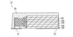
- FIG. 1 is a cross-sectional view schematically showing the structure of an example capacitor according to the present embodiment.
- 2 is a cross-sectional view schematically showing a part of the capacitor shown in FIG. 1.
- FIG. 3 is a cross-sectional view schematically showing the structure of another example of a capacitor according to the present embodiment.
- the capacitor according to this embodiment includes an anode body having a dielectric layer formed on its surface, and a conductive layer made of a metal oxide formed on the dielectric layer.
- the capacitor and the conductive layer may be hereinafter referred to as a "capacitor (C)" and a “conductive layer (L).”
- the conductive layer (L) includes a first conductive layer formed on the dielectric layer and a second conductive layer formed on the first conductive layer. The average thickness of the second conductive layer is greater than the average thickness of the first conductive layer.
- the capacitor (C) may further include a cathode extraction layer formed on the conductive layer and containing an inorganic conductive material. Since the capacitor (C) having this configuration does not include a solid electrolyte layer containing a conductive polymer, it has particularly high resistance to high temperatures.
- the average thickness T1 of the first conductive layer may be 1 nm or more, or 5 nm or more, or 1 ⁇ m, 500 nm or less, 100 nm or less, or 50 nm or less.
- the average thickness T1 of the first conductive layer may be in the range of 1 nm to 1 ⁇ m, or in the range of 5 nm to 1 ⁇ m. In any of these ranges, the upper limit may be 500 nm, 100 nm, or 50 nm.
- the average thickness T2 of the second conductive layer may be 50 nm or more, or 100 nm or more, and may be 50 ⁇ m or less, 20 ⁇ m or less, or 1 ⁇ m or less.
- the ratio T2/T1 between the average thickness T2 of the second conductive layer and the average thickness T1 of the first conductive layer is greater than 1, and may be greater than or equal to 10, greater than or equal to 1000, and less than or equal to 100000. , or 10,000 or less.
- the average thickness T1 of the first conductive layer can be measured as follows. First, a cross section of the first conductive layer is exposed, and an image of the cross section is acquired using an electron microscope. Next, ten arbitrary points are selected in the image and the thickness of the first conductive layer is measured. Then, the average thickness T1 is determined by arithmetic averaging the ten measured values obtained. The average thickness T2 of the second conductive layer is also determined in a similar manner. Note that if the boundary between the first conductive layer and the second conductive layer is unclear in the scanning electron microscope image, EDS The boundary between the two can be determined by (energy dispersive X-ray analysis) or electron diffraction.
- the anode body may include a porous portion on its surface.
- the dielectric layer is formed in the porous portion.
- the conductivity of the second conductive layer may be 1 S/cm or more, or 10 S/cm or more.
- the conductivity of the second conductive layer may be in the range of 1 S/cm to 10000 S/cm. By setting the conductivity of the second conductive layer to 1 S/cm or more, a reduction in ESR of the capacitor can be expected.
- the conductivity of the first conductive layer is also preferably within the range exemplified here.
- the conductive layer includes at least one selected from the group consisting of ZnO, TiO2 , indium tin oxide (ITO), In2O3 , SnO2 , MnO2 , NiO2 , CuInO2 , CuCrO2 , CuAlO2 , and CuScO2 . It may be composed of one type. Among these, ZnO, indium tin oxide (ITO), In 2 O 3 , CuInO 2 , and CuCrO 2 are preferable because of their high conductivity.
- ZnO and the like are sometimes classified as conductors and sometimes as semiconductors, they are treated as conductors in this specification.
- the material of the first conductive layer and the material of the second conductive layer may be different or may be the same. In order to improve the adhesion between the first conductive layer and the second conductive layer, it is preferable that the first conductive layer and the second conductive layer are made of the same material. In a preferred example, the material of the first conductive layer and the material of the second conductive layer are both ZnO or both indium tin oxide.
- the conductive layer may contain an impurity element to improve the conductivity of the conductive layer.
- concentration of the impurity element may be in the range of 0.1 to 15 atomic percent.
- the impurity element is selected depending on the material of the conductive layer. Only the first conductive layer may contain an impurity element, or only the second conductive layer may contain an impurity element. Alternatively, both the first and second conductive layers may contain an impurity element.
- Capacitor manufacturing method An example of a method for manufacturing a capacitor will be described below.
- the manufacturing method may be hereinafter referred to as "manufacturing method (M)".
- the capacitor (C) can be manufactured.
- the capacitor (C) may be manufactured by a manufacturing method other than the manufacturing method (M).
- the manufacturing method (M) includes step (i) and step (ii).
- Step (i) is a step of forming a conductive layer (L) on the dielectric layer formed on the surface of the anode body.
- Step (i) includes a step (ia) of forming a first conductive layer on the dielectric layer and a step (ib) of forming a second conductive layer on the first conductive layer. include.
- the method of forming the first and second conductive layers there is no particular limitation on the method of forming the first and second conductive layers, and any known method may be used. Examples of such formation methods include a gas phase method in which a layer is formed in a gas phase, and a liquid phase method in which a layer is formed in a liquid phase. Examples of vapor phase methods include vapor deposition, sputtering, atomic layer deposition (ALD), chemical vapor deposition (CVD), and the like. Examples of liquid phase methods include sol-gel method, chemical solution precipitation method, hydrothermal synthesis method, flux method, coating method, electrolytic plating, electroless plating, and the like. These methods are preferably selected in consideration of the material of the conductive layer.
- the first conductive layer is preferably formed using a method that provides a high coverage even when the surface is uneven.
- a method that provides a high coverage when the anode body has a porous portion on its surface, it is preferable to form the first conductive layer using a method that provides a high coverage. Examples of methods with high coverage include ALD methods.
- a preferred example of the method for forming the second conductive layer is a liquid phase method.
- the liquid phase method is preferable because it is low cost and it is easy to form a film even inside a porous structure.
- the first conductive layer is formed by an ALD method
- the second conductive layer is formed by a liquid phase method.
- the first conductive layer is made of ZnO formed by an ALD method
- the second conductive layer is made of ZnO formed by a liquid phase method.
- Step (ii) is a step of forming a cathode extraction layer on the second conductive layer.
- a capacitor element is obtained by steps (i) and (ii). After step (ii), a step of connecting a lead to the capacitor element and a step of covering the capacitor element with an exterior body are performed as necessary. In this way, the capacitor (C) is manufactured. Note that when the capacitor (C) includes a plurality of capacitor elements, the manufacturing method (M) includes a step of connecting the plurality of capacitor elements.
- the anode body can be formed using a valve metal, an alloy containing a valve metal, a compound containing a valve metal, or the like. These materials may be used alone or in combination of two or more.
- a valve metal for example, aluminum, tantalum, niobium, and titanium are preferably used.
- a foil made of the above material for example, a metal foil such as aluminum foil may be used.
- An anode body having a porous portion on the surface can be obtained, for example, by roughening the surface of a metal foil containing a valve metal.
- the surface roughening may be performed by electrolytic etching or the like.
- the anode body may be formed by sintering particles of the above material.
- the anode body may be a sintered body of tantalum.
- a porous portion is present on its surface.
- the capacitor (C) may include an anode wire partially embedded in the sintered body.
- the dielectric layer is an insulating layer that functions as a dielectric.
- the dielectric layer may be formed by anodizing the valve metal on the surface of the anode body (for example, metal foil).
- the dielectric layer only needs to be formed to cover at least a portion of the anode body.
- a dielectric layer is typically formed on the surface of the anode body. When a porous portion is present on the surface of the anode body, the dielectric layer is formed on the surface of the porous portion of the anode body.
- Typical dielectric layers include oxides of valve metals.
- a typical dielectric layer includes Ta 2 O 5 when tantalum is used as the valve metal, and a typical dielectric layer includes Al 2 O 3 when aluminum is used as the valve metal. Note that the dielectric layer is not limited to this, and may be any layer as long as it functions as a dielectric.
- the cathode extraction layer is a layer that has conductivity.
- the cathode extraction layer may be formed using conductive carbon or metal.
- the cathode extraction layer may be formed using a carbon paste containing conductive carbon particles or a metal paste containing metal particles.
- the cathode extraction layer may include a layer made only of metal (a vapor deposited layer or metal foil).
- Examples of conductive carbon include graphite, carbon black, graphene pieces, carbon nanotubes, and the like.
- metal pastes include silver pastes containing silver particles, and the like.
- the cathode extraction layer may include a first layer formed on the conductive layer (L) and a second layer formed on the first layer.
- the first layer may be a carbon layer containing conductive carbon
- the second layer may be a layer formed of metal paste.
- Lead member and exterior body There are no particular limitations on the lead member and the exterior body, and known lead members and exterior bodies may be used.
- the capacitor (C) may include only one capacitor element.
- the capacitor (C) may include multiple capacitor elements.
- the capacitor element (C) may include a plurality of capacitor elements connected in parallel.
- a plurality of capacitor elements (C) are usually connected in parallel in a stacked state and covered with an exterior body.
- FIG. 1 is a cross-sectional view schematically showing a capacitor according to a first embodiment.
- Capacitor 10 shown in FIG. 1 includes capacitor element 100, anode lead 21, cathode lead 22, metal paste layer 23, and exterior body 30.
- the capacitor element 100 includes an anode body 111, a dielectric layer 112, a conductive layer 120, and a cathode extraction layer 131.
- Dielectric layer 112 is formed to cover at least a portion of the surface of anode body 111.
- Conductive layer 120 is formed to cover at least a portion of dielectric layer 112.
- the cathode extraction layer 131 is formed to cover at least a portion of the conductive layer 120.
- the conductive layer 120 is the conductive layer (L) described above.
- the anode lead 21 is connected to the anode body 111.
- the cathode lead 22 is connected to the cathode extraction layer 131 via the metal paste layer 23.
- the metal paste layer 23 is formed of metal paste (silver paste) or the like.
- the exterior body 30 is formed to cover a portion of the anode lead 21, a portion of the cathode lead 22, and the capacitor element 100. A portion of the anode lead 21 and a portion of the cathode lead 22 are exposed from the exterior body 30 and function as terminals.
- FIG. 2 schematically shows a cross-sectional view of an example of a portion where the conductive layer 120 is present.
- the anode body 111 in the example of FIG. 2 has a porous portion 111a on the surface.
- conductive layer 120 includes a first conductive layer 121 formed on dielectric layer 112 and a second conductive layer 122 formed on first conductive layer 121.
- the average thickness of the second conductive layer 122 is greater than the average thickness of the first conductive layer 121.
- FIG. 1 shows a case where only one capacitor element 100 is included in the capacitor 10.
- capacitor 10 may include multiple capacitor elements 100.
- a cross-sectional view of an example of a capacitor 10 including a plurality of capacitor elements 100 is schematically shown in FIG. Note that in order to make the figure easier to read, illustration of some members is omitted in FIG. 3.
- the capacitor 10 in FIG. 3 includes a plurality of stacked capacitor elements 100.
- the plurality of capacitor elements 100 are connected in parallel.
- Example 2 An aluminum foil having a porous portion on the surface was prepared as an anode body. A conductive layer was formed on this aluminum foil by two methods. In the first method, a thick ZnO layer was formed only by a liquid phase method. In the second method, a thin ZnO layer (first conductive layer) was formed by an ALD method, and then a thick ZnO layer was formed by a liquid phase method. SEM-EDS measurements were performed on the cross sections of the porous portions of each of the conductive layer formed by the first method and the conductive layer formed by the second method. From the measurement results, the intensity ratio Zn/Al between Zn and Al was determined.
- the intensity ratio Zn/Al when the conductive layer was formed by the first method was 0.04, and the intensity ratio Zn/Al when the conductive layer was formed by the second method was 0.18. Ta. This result suggests that by forming the first conductive layer using the ALD method, the coverage of the conductive layer in the porous portion is improved.
- Capacitor 21 Anode lead 22 : Cathode lead 30 : Exterior body 100 : Capacitor element 111 : Anode body 111a : Porous part 112 : Dielectric layer 120 : Conductive layer 121 : First conductive layer 122 : Second conductive layer Layer 131: Cathode extraction layer
Abstract
開示されるコンデンサは、表面に誘電体層(112)が形成された陽極体(111)と、誘電体層(112)上に形成された金属酸化物からなる導電層(120)と、を含む。導電層(120)は、誘電体層(112)上に形成された第1の導電層(121)と、第1の導電層(121)上に形成された第2の導電層(122)とを含む。第2の導電層(122)の平均厚さは第1の導電層(121)の平均厚さよりも大きい。
Description
本開示は、コンデンサに関する。
従来から、様々なコンデンサが提案されている。特許文献1(特開2017-103412号公報)は、「陽極体と、前記陽極体の表面に配置された誘電体層と、前記誘電体層の表面に配置され、1(S/cm)以上の導電率を有する酸化亜鉛を用いて構成された固体電解質層と、を備える、固体電解コンデンサ。」を開示している。
特許文献2(特開2020-35890号公報)は、「弁金属からなる陽極体と、前記陽極体の表面に形成された誘電体層と、前記誘電体層の上に形成された半導体層と、前記半導体層の上に形成された陰極層と、を備え、前記半導体層は、p型無機半導体を用いて構成されている、固体電解コンデンサ。」を開示している。
現在、高温に対する耐性が高いコンデンサが求められている。そのような状況において、本開示の目的の1つは、高温に対する耐性が高い新規なコンデンサを提供することである。
本開示の一局面は、コンデンサに関する。当該コンデンサは、表面に誘電体層が形成された陽極体と、前記誘電体層上に形成された金属酸化物からなる導電層と、を含み、前記導電層は、前記誘電体層上に形成された第1の導電層と、前記第1の導電層上に形成された第2の導電層とを含み、前記第2の導電層の平均厚さは前記第1の導電層の平均厚さよりも大きい。
本開示によれば、高温に対する耐性が高いコンデンサが得られる。
本発明の新規な特徴を添付の請求の範囲に記述するが、本発明は、構成および内容の両方に関し、本発明の他の目的および特徴と併せ、図面を照合した以下の詳細な説明によりさらによく理解されるであろう。
本発明の新規な特徴を添付の請求の範囲に記述するが、本発明は、構成および内容の両方に関し、本発明の他の目的および特徴と併せ、図面を照合した以下の詳細な説明によりさらによく理解されるであろう。
以下では、本開示に係る実施形態について例を挙げて説明するが、本開示は以下で説明する例に限定されない。以下の説明では、具体的な数値や材料を例示する場合があるが、本開示に係る発明を実施できる限り、他の数値や他の材料を適用してもよい。この明細書において、「数値A~数値B」という記載は、数値Aおよび数値Bを含み、「数値A以上で数値B以下」と読み替えることが可能である。以下の説明において、特定の物性や条件などに関する数値の下限と上限とを例示した場合、下限が上限以上とならない限り、例示した下限のいずれかと例示した上限のいずれかとを任意に組み合わせることができる。
(コンデンサ)
本実施形態に係るコンデンサは、表面に誘電体層が形成された陽極体と、当該誘電体層上に形成された金属酸化物からなる導電層と、を含む。当該コンデンサおよび当該導電層を以下では、「コンデンサ(C)」および「導電層(L)」と称する場合がある。導電層(L)は、誘電体層上に形成された第1の導電層と、第1の導電層上に形成された第2の導電層とを含む。第2の導電層の平均厚さは第1の導電層の平均厚さよりも大きい。
本実施形態に係るコンデンサは、表面に誘電体層が形成された陽極体と、当該誘電体層上に形成された金属酸化物からなる導電層と、を含む。当該コンデンサおよび当該導電層を以下では、「コンデンサ(C)」および「導電層(L)」と称する場合がある。導電層(L)は、誘電体層上に形成された第1の導電層と、第1の導電層上に形成された第2の導電層とを含む。第2の導電層の平均厚さは第1の導電層の平均厚さよりも大きい。
コンデンサ(C)では、薄い第1の導電層によって応力を緩和できるため、高温にさらされたときでも導電層(L)が誘電体層から剥離することを抑制できる。
コンデンサ(C)は、導電層上に形成された、無機導電材料を含む陰極引出層をさらに含んでもよい。この構成を有するコンデンサ(C)は、導電性高分子を含む固体電解質層を含まないため、高温に対する耐性が特に高い。
第1の導電層の平均厚さT1は、1nm以上、または5nm以上であってもよく、1μm、500nm以下、100nm以下、または50nm以下であってもよい。第1の導電層の平均厚さT1は、1nm~1μmの範囲、または5nm~1μmの範囲にあってもよい。これらの範囲のいずれかにおいて、上限を、500nm、100nm、または50nmとしてもよい。
第2の導電層の平均厚さT2は、50nm以上、または100nm以上であってもよく、50μm以下、20μm以下、または1μm以下であってもよい。
第2の導電層の平均厚さT2と第1の導電層の平均厚さT1との比T2/T1は、1より大きく、10以上、100以上、または1000以上であってもよく、100000以下、または10000以下であってもよい。
第1の導電層の平均厚さT1は、以下のようにして測定できる。まず、第1の導電層の断面を露出させ、当該断面の画像を電子顕微鏡で取得する。次に、当該画像において任意の10点を選択して第1の導電層の厚さを測定する。そして、得られた10個の測定値を算術平均することによって、平均厚さT1が求められる。第2の導電層の平均厚さT2も、同様の方法で求められる。なお、第1の導電層と第2の導電層との境界が走査型電子顕微鏡の画像では不明確な場合、STEM(走査型透過電子顕微鏡)もしくはTEM(透過型電子顕微鏡)を用いて、EDS(エネルギー分散型X線分析)や、電子線回折法によって、両者の境界を判別できる。
陽極体は、その表面に多孔質部を含んでもよい。その場合、誘電体層は、当該多孔質部に形成されている。
第2の導電層の導電率は、1S/cm以上、または10S/cm以上であってもよい。第2の導電層の導電率は、1S/cm~10000S/cmの範囲にあってもよい。第2の導電層の導電率を1S/cm以上とすることによって、コンデンサのESR低減が期待できる。第1の導電層の導電率も、ここに例示した範囲にあることが好ましい。
導電層は、ZnO、TiO2、酸化インジウムスズ(ITO)、In2O3、SnO2、MnO2、NiO2、CuInO2、CuCrO2、CuAlO2、およびCuScO2からなる群より選択される少なくとも1種で構成されていてもよい。これらの中でも、導電率が高い点で、ZnO、酸化インジウムスズ(ITO)、In2O3、CuInO2、CuCrO2が好ましい。
なお、ZnOなどは、導電体として分類されることがある一方で、半導体として分類されることもあるが、この明細書では導電体として扱う。
第1の導電層の材料と第2の導電層の材料とは異なっていてもよいし、同じであってもよい。第1の導電層と第2の導電層との密着性を高めるため、両者は同じ材料で形成されていることが好ましい。好ましい一例では、第1の導電層の材料および第2の導電層の材料が共にZnOであるか、または、共に酸化インジウムスズである。
導電層は、導電層の導電性を向上させるための不純物元素を含んでもよい。不純物元素の濃度は、0.1~15原子%の範囲にあってもよい。不純物元素は、導電層の材料に応じて選択される。第1の導電層のみが不純物元素を含んでもよいし、第2の導電層のみが不純物元素を含んでもよい。あるいは、第1および第2の導電層の両方が不純物元素を含んでもよい。
(コンデンサの製造方法)
コンデンサの製造方法の一例について以下に説明する。当該製造方法を以下では「製造方法(M)」と称する場合がある。製造方法(M)によれば、コンデンサ(C)を製造できる。ただし、コンデンサ(C)は、製造方法(M)以外の製造方法で製造してもよい。
コンデンサの製造方法の一例について以下に説明する。当該製造方法を以下では「製造方法(M)」と称する場合がある。製造方法(M)によれば、コンデンサ(C)を製造できる。ただし、コンデンサ(C)は、製造方法(M)以外の製造方法で製造してもよい。
製造方法(M)は、工程(i)および工程(ii)を含む。工程(i)は、陽極体の表面に形成された誘電体層上に、導電層(L)を形成する工程である。工程(i)は、誘電体層上に第1の導電層を形成する工程(i-a)と、第1の導電層上に第2の導電層を形成する工程(i-b)とを含む。
第1および第2の導電層の形成方法に特に限定はなく、公知の方法で形成してもよい。それらの形成方法の例には、気相で層を形成する気相法や、液相で層を形成する液相法が含まれる。気相法の例には、蒸着法、スパッタリング法、原子層堆積法(ALD法)、化学気相成長法(CVD法)などが含まれる。液相法の例には、ゾルゲル法、化学溶液析出法、水熱合成法、フラックス法、塗布法、電解めっき、無電解めっきなどが含まれる。これらの方法は、導電層の材料を考慮して選択することが好ましい。
第1の導電層は、表面に凹凸がある場合でも被覆率が高い方法で形成することが好ましい。特に、陽極体がその表面に多孔質部を有する場合、被覆率が高い方法で第1の導電層を形成することが好ましい。被覆率が高い方法の例には、ALD法が含まれる。
第2の導電層の形成方法の好ましい一例は、液相法である。液相法は、コストが低い点、多孔質の内部にも成膜しやすい点で、好ましい。
好ましい一例では、第1の導電層をALD法で形成し、第2の導電層を液相法で形成する。導電層の好ましい一例では、第1の導電層がALD法で形成されたZnOからなり、第2の導電層が液相法で形成されたZnOからなる。
工程(ii)は、第2の導電層上に、陰極引出層を形成する工程である。工程(i)および工程(ii)によって、コンデンサ素子が得られる。工程(ii)の後は、必要に応じて、コンデンサ素子にリードを接続する工程、および、コンデンサ素子を外装体で覆う工程が行われる。このようにして、コンデンサ(C)が製造される。なお、コンデンサ(C)が複数のコンデンサ素子を含む場合、製造方法(M)は、複数のコンデンサ素子を接続する工程を含む。
コンデンサ(C)の構成および構成部材の例について、以下に説明する。本開示に特徴的な部分以外の構成部材には、公知の構成部材を適用してもよい。
(陽極体)
陽極体は、弁作用金属、弁作用金属を含む合金、および弁作用金属を含む化合物などを用いて形成できる。これらの材料は、一種を単独で使用してもよいし、二種以上を組み合わせて使用してもよい。弁作用金属としては、例えば、アルミニウム、タンタル、ニオブ、チタンが好ましく使用される。陽極体には、上記の材料の箔(例えばアルミニウム箔などの金属箔)を用いてもよい。
陽極体は、弁作用金属、弁作用金属を含む合金、および弁作用金属を含む化合物などを用いて形成できる。これらの材料は、一種を単独で使用してもよいし、二種以上を組み合わせて使用してもよい。弁作用金属としては、例えば、アルミニウム、タンタル、ニオブ、チタンが好ましく使用される。陽極体には、上記の材料の箔(例えばアルミニウム箔などの金属箔)を用いてもよい。
表面に多孔質部を有する陽極体は、例えば、弁作用金属を含む金属箔の表面を粗面化することによって得られる。粗面化は、電解エッチング等によって行ってもよい。
あるいは、陽極体は、上記材料の粒子を焼結することによって形成してもよい。例えば、陽極体はタンタルの焼結体であってもよい。陽極体が焼結体である場合、その表面には多孔質部が存在する。陽極体が焼結体である場合、コンデンサ(C)は、一部が焼結体に埋め込まれた陽極ワイヤを含んでもよい。
(誘電体層)
誘電体層は、誘電体として機能する絶縁性の層である。誘電体層は、陽極体(例えば金属箔)の表面の弁作用金属を、陽極酸化することによって形成してもよい。誘電体層は、陽極体の少なくとも一部を覆うように形成されていればよい。誘電体層は、通常、陽極体の表面に形成される。陽極体の表面に多孔質部が存在する場合、誘電体層は、陽極体の多孔質部の表面に形成される。
誘電体層は、誘電体として機能する絶縁性の層である。誘電体層は、陽極体(例えば金属箔)の表面の弁作用金属を、陽極酸化することによって形成してもよい。誘電体層は、陽極体の少なくとも一部を覆うように形成されていればよい。誘電体層は、通常、陽極体の表面に形成される。陽極体の表面に多孔質部が存在する場合、誘電体層は、陽極体の多孔質部の表面に形成される。
典型的な誘電体層は、弁作用金属の酸化物を含む。例えば、弁作用金属としてタンタルを用いた場合の典型的な誘電体層はTa2O5を含み、弁作用金属としてアルミニウムを用いた場合の典型的な誘電体層はAl2O3を含む。尚、誘電体層はこれに限らず、誘電体として機能するものであればよい。
(陰極引出層)
陰極引出層は、導電性を有する層である。陰極引出層は、導電性カーボンや金属を用いて形成してもよい。具体的には、陰極引出層は、導電性カーボンの粒子を含むカーボンペーストや、金属粒子を含む金属ペーストを用いて形成してもよい。あるいは、陰極引出層は、金属のみからなる層(蒸着層や金属箔)を含んでもよい。導電性カーボンの例には、グラファイト、カーボンブラック、グラフェン片、カーボンナノチューブなどが含まれる。金属ペーストの例には、銀粒子を含む銀ペーストなどが含まれる。
陰極引出層は、導電性を有する層である。陰極引出層は、導電性カーボンや金属を用いて形成してもよい。具体的には、陰極引出層は、導電性カーボンの粒子を含むカーボンペーストや、金属粒子を含む金属ペーストを用いて形成してもよい。あるいは、陰極引出層は、金属のみからなる層(蒸着層や金属箔)を含んでもよい。導電性カーボンの例には、グラファイト、カーボンブラック、グラフェン片、カーボンナノチューブなどが含まれる。金属ペーストの例には、銀粒子を含む銀ペーストなどが含まれる。
陰極引出層は、導電層(L)上に形成された第1の層と、第1の層上に形成された第2の層とを含んでもよい。その場合、第1の層は、導電性カーボンを含むカーボン層であってもよく、第2の層は、金属ペーストで形成された層であってもよい。
(リード部材および外装体)
リード部材および外装体に特に限定はなく、公知のリード部材および外装体を用いてもよい。
リード部材および外装体に特に限定はなく、公知のリード部材および外装体を用いてもよい。
(コンデンサ(C)の構造)
コンデンサ(C)は、コンデンサ素子を1つだけ含んでもよい。あるいは、コンデンサ(C)は、複数のコンデンサ素子を含んでもよい。例えば、コンデンサ素子(C)は、並列に接続された複数のコンデンサ素子を含んでもよい。複数のコンデンサ素子(C)は、通常、積層された状態で並列に接続され、外装体で覆われる。
コンデンサ(C)は、コンデンサ素子を1つだけ含んでもよい。あるいは、コンデンサ(C)は、複数のコンデンサ素子を含んでもよい。例えば、コンデンサ素子(C)は、並列に接続された複数のコンデンサ素子を含んでもよい。複数のコンデンサ素子(C)は、通常、積層された状態で並列に接続され、外装体で覆われる。
本開示に係る実施形態の例について、図面を参照して以下に具体的に説明する。以下で説明する例の構成要素には、上述した構成要素を適用できる。また、以下で説明する例は、上述した記載に基づいて変更できる。また、以下で説明する事項を、上記の実施形態に適用してもよい。また、以下で説明する実施形態において、本開示のコンデンサに必須ではない構成要素は省略してもよい。なお、以下の図は模式的なものであり、実際の構成とは異なる場合がある。
(実施形態1)
図1は、実施形態1に係るコンデンサを模式的に示す断面図である。図1に示すコンデンサ10は、コンデンサ素子100、陽極リード21、陰極リード22、金属ペースト層23、および外装体30を含む。
図1は、実施形態1に係るコンデンサを模式的に示す断面図である。図1に示すコンデンサ10は、コンデンサ素子100、陽極リード21、陰極リード22、金属ペースト層23、および外装体30を含む。
コンデンサ素子100は、陽極体111、誘電体層112、導電層120、および陰極引出層131を含む。誘電体層112は、陽極体111の表面の少なくとも一部を覆うように形成されている。導電層120は、誘電体層112の少なくとも一部を覆うように形成されている。陰極引出層131は、導電層120の少なくとも一部を覆うように形成されている。導電層120は、上述した導電層(L)である。
陽極リード21は、陽極体111に接続されている。陰極リード22は、金属ペースト層23を介して陰極引出層131に接続されている。金属ペースト層23は、金属ペースト(銀ペースト)などで形成される。外装体30は、陽極リード21の一部、陰極リード22の一部、およびコンデンサ素子100を覆うように形成されている。陽極リード21の一部および陰極リード22の一部は外装体30から露出しており、端子として機能する。
導電層120が存在する部分の一例の断面図を図2に模式的に示す。図2の一例の陽極体111は、表面に多孔質部111aを有する。図2に示すように、導電層120は、誘電体層112上に形成された第1の導電層121と、第1の導電層121上に形成された第2の導電層122とを含む。第2の導電層122の平均厚さは、第1の導電層121の平均厚さよりも大きい。
図1には、コンデンサ10に含まれるコンデンサ素子100が1つだけである場合を示した。しかし、コンデンサ10は、複数のコンデンサ素子100を含んでもよい。複数のコンデンサ素子100を含むコンデンサ10の一例の断面図を図3に模式的に示す。なお、図を見やすくするために、図3では、一部の部材の図示を省略する。
図3のコンデンサ10は積層された複数のコンデンサ素子100を含む。複数のコンデンサ素子100は、並列に接続されている。
(実施例)
陽極体として、表面に多孔質部を有するアルミニウム箔を準備した。このアルミニウム箔に、2つの方法によって導電層を形成した。第1の方法では、液相法のみによって厚いZnO層を形成した。第2の方法では、薄いZnO層(第1の導電層)をALD法で形成した後に、厚いZnO層を液相法によって形成した。第1の方法で形成された導電層および第2の方法で形成された導電層のそれぞれについて、多孔質部の断面のSEM-EDS測定を行った。その測定結果から、ZnとAlとの強度比Zn/Alを求めた。その結果、第1の方法で導電層を形成した場合の強度比Zn/Alは0.04であり、第2の方法で導電層を形成した場合の強度比Zn/Alは0.18であった。この結果は、ALD法で第1の導電層を形成することによって、多孔質部における導電層の被覆性が向上することを示唆している。
陽極体として、表面に多孔質部を有するアルミニウム箔を準備した。このアルミニウム箔に、2つの方法によって導電層を形成した。第1の方法では、液相法のみによって厚いZnO層を形成した。第2の方法では、薄いZnO層(第1の導電層)をALD法で形成した後に、厚いZnO層を液相法によって形成した。第1の方法で形成された導電層および第2の方法で形成された導電層のそれぞれについて、多孔質部の断面のSEM-EDS測定を行った。その測定結果から、ZnとAlとの強度比Zn/Alを求めた。その結果、第1の方法で導電層を形成した場合の強度比Zn/Alは0.04であり、第2の方法で導電層を形成した場合の強度比Zn/Alは0.18であった。この結果は、ALD法で第1の導電層を形成することによって、多孔質部における導電層の被覆性が向上することを示唆している。
本開示は、コンデンサに利用できる。
本発明を現時点での好ましい実施態様に関して説明したが、そのような開示を限定的に解釈してはならない。種々の変形および改変は、上記開示を読むことによって本発明に属する技術分野における当業者には間違いなく明らかになるであろう。したがって、添付の請求の範囲は、本発明の真の精神および範囲から逸脱することなく、すべての変形および改変を包含する、と解釈されるべきものである。
本発明を現時点での好ましい実施態様に関して説明したが、そのような開示を限定的に解釈してはならない。種々の変形および改変は、上記開示を読むことによって本発明に属する技術分野における当業者には間違いなく明らかになるであろう。したがって、添付の請求の範囲は、本発明の真の精神および範囲から逸脱することなく、すべての変形および改変を包含する、と解釈されるべきものである。
10 :コンデンサ
21 :陽極リード
22 :陰極リード
30 :外装体
100 :コンデンサ素子
111 :陽極体
111a :多孔質部
112 :誘電体層
120 :導電層
121 :第1の導電層
122 :第2の導電層
131 :陰極引出層
21 :陽極リード
22 :陰極リード
30 :外装体
100 :コンデンサ素子
111 :陽極体
111a :多孔質部
112 :誘電体層
120 :導電層
121 :第1の導電層
122 :第2の導電層
131 :陰極引出層
Claims (7)
- コンデンサであって、
表面に誘電体層が形成された陽極体と、
前記誘電体層上に形成された金属酸化物からなる導電層と、を含み、
前記導電層は、前記誘電体層上に形成された第1の導電層と、前記第1の導電層上に形成された第2の導電層とを含み、
前記第2の導電層の平均厚さは前記第1の導電層の平均厚さよりも大きい、コンデンサ。 - 前記導電層上に形成された、無機導電材料を含む陰極引出層をさらに含む、請求項1に記載のコンデンサ。
- 前記第1の導電層の平均厚さは、1nm~1μmの範囲にある、請求項1または2に記載のコンデンサ。
- 前記陽極体は、前記表面に多孔質部を含み、
前記誘電体層は前記多孔質部に形成されている、請求項1~3のいずれか1項に記載のコンデンサ。 - 前記第2の導電層の導電率は、1S/cm以上である、請求項1~4のいずれか1項に記載のコンデンサ。
- 前記導電層は、ZnO、TiO2、酸化インジウムスズ、In2O3、SnO2、MnO2、NiO2、CuInO2、CuCrO2、CuAlO2、およびCuScO2からなる群より選択される少なくとも1種で構成されている、請求項1~5のいずれか1項に記載のコンデンサ。
- 前記導電層は、前記導電層の導電性を向上させるための不純物元素を含む、請求項1~6のいずれか1項に記載のコンデンサ。
Applications Claiming Priority (2)
| Application Number | Priority Date | Filing Date | Title |
|---|---|---|---|
| JP2022-036524 | 2022-03-09 | ||
| JP2022036524 | 2022-03-09 |
Publications (1)
| Publication Number | Publication Date |
|---|---|
| WO2023171426A1 true WO2023171426A1 (ja) | 2023-09-14 |
Family
ID=87935137
Family Applications (1)
| Application Number | Title | Priority Date | Filing Date |
|---|---|---|---|
| PCT/JP2023/006860 WO2023171426A1 (ja) | 2022-03-09 | 2023-02-24 | コンデンサ |
Country Status (1)
| Country | Link |
|---|---|
| WO (1) | WO2023171426A1 (ja) |
Citations (3)
| Publication number | Priority date | Publication date | Assignee | Title |
|---|---|---|---|---|
| JP2005294401A (ja) * | 2004-03-31 | 2005-10-20 | Sanyo Electric Co Ltd | 固体電解コンデンサおよびその製造方法 |
| JP2017103412A (ja) * | 2015-12-04 | 2017-06-08 | 株式会社トーキン | 固体電解コンデンサ |
| JP2020035890A (ja) * | 2018-08-30 | 2020-03-05 | 株式会社トーキン | 固体電解コンデンサ、及び固体電解コンデンサの製造方法 |
-
2023
- 2023-02-24 WO PCT/JP2023/006860 patent/WO2023171426A1/ja unknown
Patent Citations (3)
| Publication number | Priority date | Publication date | Assignee | Title |
|---|---|---|---|---|
| JP2005294401A (ja) * | 2004-03-31 | 2005-10-20 | Sanyo Electric Co Ltd | 固体電解コンデンサおよびその製造方法 |
| JP2017103412A (ja) * | 2015-12-04 | 2017-06-08 | 株式会社トーキン | 固体電解コンデンサ |
| JP2020035890A (ja) * | 2018-08-30 | 2020-03-05 | 株式会社トーキン | 固体電解コンデンサ、及び固体電解コンデンサの製造方法 |
Similar Documents
| Publication | Publication Date | Title |
|---|---|---|
| US8116068B2 (en) | Solid electrolytic capacitor | |
| JP5458271B2 (ja) | 色素増感太陽電池およびその製造方法 | |
| WO2009125620A1 (ja) | コンデンサおよびその製造方法 | |
| CN109564970B (zh) | 二次电池 | |
| JP4834193B2 (ja) | 電極構造体の製造方法、電極構造体およびコンデンサ | |
| WO2023171426A1 (ja) | コンデンサ | |
| JP2009071300A (ja) | 固体電解コンデンサ | |
| JP2010212594A (ja) | 固体電解コンデンサ及びその製造方法 | |
| US5938797A (en) | Low impedance solid electrolytic capacitor and method for fabricating the same | |
| US8587928B2 (en) | Electrode for capacitor and capacitor | |
| WO2020162459A1 (en) | Capacitor | |
| TW529049B (en) | Electrode and capacitor with the electrode | |
| US7885054B2 (en) | Solid electrolytic capacitor | |
| JPH03150822A (ja) | 電解コンデンサ用アルミニウム電極 | |
| WO2023176381A1 (ja) | コンデンサ | |
| US20230250542A1 (en) | Electrode | |
| WO2021200452A1 (ja) | 固体電解コンデンサ | |
| US3182235A (en) | Electrical capacitor and titaniumcontaining electrode material therefor | |
| EP4187239A1 (en) | Electrode | |
| Mozalev et al. | Porous-Anodic-Alumina-Templated Ta-Nb-Alloy/Oxide Coatings Via the Magnetron-Sputtering/Anodizing as Novel 3d Nanostructured Electrodes for Energy-Storage Applications | |
| JP2020053592A (ja) | 固体電解コンデンサおよびその製造方法 | |
| JP2013077676A (ja) | 電極構造体の製造方法、電極構造体およびコンデンサ | |
| TW201830430A (zh) | 電容器封裝結構及其抗氧化複合式電極箔 |
Legal Events
| Date | Code | Title | Description |
|---|---|---|---|
| 121 | Ep: the epo has been informed by wipo that ep was designated in this application |
Ref document number: 23766604 Country of ref document: EP Kind code of ref document: A1 |