WO2023171139A1 - 半導体装置 - Google Patents
半導体装置 Download PDFInfo
- Publication number
- WO2023171139A1 WO2023171139A1 PCT/JP2023/001366 JP2023001366W WO2023171139A1 WO 2023171139 A1 WO2023171139 A1 WO 2023171139A1 JP 2023001366 W JP2023001366 W JP 2023001366W WO 2023171139 A1 WO2023171139 A1 WO 2023171139A1
- Authority
- WO
- WIPO (PCT)
- Prior art keywords
- region
- gate
- gate region
- bottom gate
- layer
- Prior art date
- Legal status (The legal status is an assumption and is not a legal conclusion. Google has not performed a legal analysis and makes no representation as to the accuracy of the status listed.)
- Ceased
Links
Images




Classifications
-
- H—ELECTRICITY
- H10—SEMICONDUCTOR DEVICES; ELECTRIC SOLID-STATE DEVICES NOT OTHERWISE PROVIDED FOR
- H10D—INORGANIC ELECTRIC SEMICONDUCTOR DEVICES
- H10D30/00—Field-effect transistors [FET]
- H10D30/01—Manufacture or treatment
- H10D30/051—Manufacture or treatment of FETs having PN junction gates
-
- H—ELECTRICITY
- H10—SEMICONDUCTOR DEVICES; ELECTRIC SOLID-STATE DEVICES NOT OTHERWISE PROVIDED FOR
- H10D—INORGANIC ELECTRIC SEMICONDUCTOR DEVICES
- H10D30/00—Field-effect transistors [FET]
- H10D30/80—FETs having rectifying junction gate electrodes
- H10D30/83—FETs having PN junction gate electrodes
-
- H—ELECTRICITY
- H10—SEMICONDUCTOR DEVICES; ELECTRIC SOLID-STATE DEVICES NOT OTHERWISE PROVIDED FOR
- H10D—INORGANIC ELECTRIC SEMICONDUCTOR DEVICES
- H10D30/00—Field-effect transistors [FET]
- H10D30/80—FETs having rectifying junction gate electrodes
- H10D30/87—FETs having Schottky gate electrodes, e.g. metal-semiconductor FETs [MESFET]
-
- H—ELECTRICITY
- H10—SEMICONDUCTOR DEVICES; ELECTRIC SOLID-STATE DEVICES NOT OTHERWISE PROVIDED FOR
- H10D—INORGANIC ELECTRIC SEMICONDUCTOR DEVICES
- H10D62/00—Semiconductor bodies, or regions thereof, of devices having potential barriers
- H10D62/10—Shapes, relative sizes or dispositions of the regions of the semiconductor bodies; Shapes of the semiconductor bodies
- H10D62/102—Constructional design considerations for preventing surface leakage or controlling electric field concentration
- H10D62/103—Constructional design considerations for preventing surface leakage or controlling electric field concentration for increasing or controlling the breakdown voltage of reverse-biased devices
- H10D62/105—Constructional design considerations for preventing surface leakage or controlling electric field concentration for increasing or controlling the breakdown voltage of reverse-biased devices by having particular doping profiles, shapes or arrangements of PN junctions; by having supplementary regions, e.g. junction termination extension [JTE]
- H10D62/106—Constructional design considerations for preventing surface leakage or controlling electric field concentration for increasing or controlling the breakdown voltage of reverse-biased devices by having particular doping profiles, shapes or arrangements of PN junctions; by having supplementary regions, e.g. junction termination extension [JTE] having supplementary regions doped oppositely to or in rectifying contact with regions of the semiconductor bodies, e.g. guard rings with PN or Schottky junctions
- H10D62/107—Buried supplementary regions, e.g. buried guard rings
-
- H—ELECTRICITY
- H10—SEMICONDUCTOR DEVICES; ELECTRIC SOLID-STATE DEVICES NOT OTHERWISE PROVIDED FOR
- H10D—INORGANIC ELECTRIC SEMICONDUCTOR DEVICES
- H10D62/00—Semiconductor bodies, or regions thereof, of devices having potential barriers
- H10D62/10—Shapes, relative sizes or dispositions of the regions of the semiconductor bodies; Shapes of the semiconductor bodies
- H10D62/124—Shapes, relative sizes or dispositions of the regions of semiconductor bodies or of junctions between the regions
- H10D62/126—Top-view geometrical layouts of the regions or the junctions
- H10D62/127—Top-view geometrical layouts of the regions or the junctions of cellular field-effect devices, e.g. multicellular DMOS transistors or IGBTs
-
- H—ELECTRICITY
- H10—SEMICONDUCTOR DEVICES; ELECTRIC SOLID-STATE DEVICES NOT OTHERWISE PROVIDED FOR
- H10D—INORGANIC ELECTRIC SEMICONDUCTOR DEVICES
- H10D62/00—Semiconductor bodies, or regions thereof, of devices having potential barriers
- H10D62/10—Shapes, relative sizes or dispositions of the regions of the semiconductor bodies; Shapes of the semiconductor bodies
- H10D62/17—Semiconductor regions connected to electrodes not carrying current to be rectified, amplified or switched, e.g. channel regions
- H10D62/343—Gate regions of field-effect devices having PN junction gates
-
- H—ELECTRICITY
- H10—SEMICONDUCTOR DEVICES; ELECTRIC SOLID-STATE DEVICES NOT OTHERWISE PROVIDED FOR
- H10D—INORGANIC ELECTRIC SEMICONDUCTOR DEVICES
- H10D62/00—Semiconductor bodies, or regions thereof, of devices having potential barriers
- H10D62/10—Shapes, relative sizes or dispositions of the regions of the semiconductor bodies; Shapes of the semiconductor bodies
- H10D62/17—Semiconductor regions connected to electrodes not carrying current to be rectified, amplified or switched, e.g. channel regions
- H10D62/393—Body regions of DMOS transistors or IGBTs
-
- H—ELECTRICITY
- H10—SEMICONDUCTOR DEVICES; ELECTRIC SOLID-STATE DEVICES NOT OTHERWISE PROVIDED FOR
- H10D—INORGANIC ELECTRIC SEMICONDUCTOR DEVICES
- H10D64/00—Electrodes of devices having potential barriers
- H10D64/20—Electrodes characterised by their shapes, relative sizes or dispositions
- H10D64/27—Electrodes not carrying the current to be rectified, amplified, oscillated or switched, e.g. gates
- H10D64/311—Gate electrodes for field-effect devices
- H10D64/411—Gate electrodes for field-effect devices for FETs
- H10D64/511—Gate electrodes for field-effect devices for FETs for IGFETs
- H10D64/517—Gate electrodes for field-effect devices for FETs for IGFETs characterised by the conducting layers
- H10D64/519—Gate electrodes for field-effect devices for FETs for IGFETs characterised by the conducting layers characterised by their top-view geometrical layouts
Definitions
- the present disclosure relates to a semiconductor device.
- Patent Document 1 discloses a junction field effect transistor.
- a junction field effect transistor an n ⁇ type epitaxial layer is stacked on a semiconductor substrate.
- a plurality of gate regions are formed at intervals, and source regions are formed between adjacent gate regions at intervals from the gate regions.
- a gate electrode and a source electrode are connected to the gate region and the source region, respectively.
- the drain electrode is connected to the back surface of the semiconductor substrate.
- An embodiment of the present disclosure provides a semiconductor device that can form a junction field effect transistor that can reduce gate current.
- a semiconductor device includes a semiconductor layer having a first surface, a bottom gate region of a first conductivity type formed in the semiconductor layer, and a surface layer portion of the first surface of the semiconductor layer. a top gate region of a first conductivity type that is formed and faces the bottom gate region in the thickness direction of the semiconductor layer; and a top gate region of a first conductivity type that is formed in a surface layer portion of the first surface of the semiconductor layer in a direction along the first surface.
- a semiconductor device can be provided.
- FIG. 1 is a schematic perspective view of a semiconductor device according to an embodiment of the present disclosure.
- 2 is a schematic plan view of the first element region of FIG. 1.
- FIG. 3 is a cross-sectional view taken along line III-III in FIG. 2.
- FIG. 4 is a cross-sectional view for explaining the configuration of an n-channel JFET according to a comparative example.
- FIG. 5 is a diagram for explaining the operation of the n-channel JFET in FIG. 4.
- FIG. 6 is a diagram for explaining the operation of the n-channel JFET in FIG. 4.
- FIG. 7A is a simulation image showing impact ionization in an n-channel JFET according to a comparative example when the drain-source voltage Vds is 30V.
- FIG. 1 is a schematic perspective view of a semiconductor device according to an embodiment of the present disclosure.
- FIG. 3 is a cross-sectional view taken along line III-III in FIG. 2.
- FIG. 4 is a cross-
- FIG. 7B is a simulation image showing impact ionization in the n-channel JFET according to this embodiment when the drain-source voltage Vds is 30V.
- FIG. 8 is a flowchart showing a part of the manufacturing process of the semiconductor device.
- FIG. 9 is a schematic plan view for explaining a p-channel JFET according to an embodiment of the present disclosure.
- FIG. 10 is a sectional view taken along line XX in FIG. 9.
- FIG. 11 is a flowchart showing a part of the manufacturing process of the JFET shown in FIG.
- FIG. 1 is a schematic perspective view of a semiconductor device 1 according to an embodiment of the present disclosure.
- the semiconductor device 1 includes, for example, a chip-shaped integrated circuit (IC) device.
- the semiconductor device 1 is classified into SSI (Small Scale IC), MSI (Middle Scale IC), LSI (Large Scale IC), VLSI (Very Large Scale IC), and ULSI (Ultra Large Scale IC) based on the number of integrated circuit elements. IC).
- SSI Small Scale IC
- MSI Middle Scale IC
- LSI Large Scale IC
- VLSI Very Large Scale IC
- ULSI Ultra Large Scale IC
- the semiconductor device 1 has a plurality of element regions 2 in which circuit elements are formed. Each of the plurality of element regions 2 is a region in which a functional device is formed, and is insulated and isolated from other element regions.
- the functional device may include, for example, at least one of a semiconductor switching device, a semiconductor rectifying device, and a passive device.
- the functional device may include, for example, a circuitry combining at least two of a semiconductor switching device, a semiconductor rectifying device, and a passive device.
- the semiconductor switching device may include, for example, at least one of a MOSFET (Metal Oxide Semiconductor Field Effect Transistor), a BJT (Bipolar Junction Transistor), an IGBT (Insulated Gate Bipolar Junction Transistor), and a JFET (Junction Field Effect Transistor).
- the semiconductor rectifier device may include, for example, at least one of a pn junction diode, a pin junction diode, a Zener diode, a Schottky barrier diode, and a fast recovery diode.
- Passive devices may include, for example, at least one of a resistor, a capacitor, and an inductor.
- the plurality of element regions 2 include a first element region 2A.
- the first element region 2A may be a JFET element region in which an n-channel JFET 3 is formed as a circuit element. Although four element regions 2 are shown in FIG. 1, the semiconductor device 1 may have a larger number of element regions.
- FIG. 2 is a schematic plan view of the first element region 2A (n-channel JFET 3) in FIG. 1.
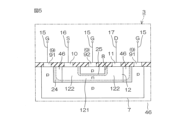
- FIG. 3 is a cross-sectional view taken along line III-III in FIG. 2.
- a semiconductor device 1 includes a semiconductor substrate 4, an element isolation section 5, a buried layer 6, a bottom gate region 7, a top gate region 8, a gate contact region 9, a source region 10, and a drain region 11. , a channel region 12 , and a field insulating film 13 .
- the channel region 12 is selectively hatched to aid in understanding the structure.
- the semiconductor substrate 4 may include a base substrate 41 and an epitaxial layer 42 as an example of a semiconductor layer.
- the base substrate 41 is formed of a silicon (Si) substrate in this embodiment, it may be a substrate formed of another material (for example, silicon carbide (SiC), etc.).
- Base substrate 41 is p - type in this embodiment.
- the base substrate 41 may have an impurity concentration of, for example, 1 ⁇ 10 14 cm ⁇ 3 or more and 5 ⁇ 10 18 cm ⁇ 3 or less. Further, the thickness of the base substrate 41 may be, for example, 500 ⁇ m or more and 800 ⁇ m or less before grinding.
- the epitaxial layer 42 is in contact with the base substrate 41 and is laminated on the base substrate 41.
- the epitaxial layer 42 has an element main surface 43 and a bonding surface 44 facing opposite to the element main surface 43 in the thickness direction of the epitaxial layer 42 .
- the element main surface 43 is a surface on which the element region 2 (first element region 2A in FIGS. 2 and 3) is formed.
- the bonding surface 44 is a surface in contact with the base substrate 41.
- Epitaxial layer 42 has a conductivity type opposite to that of base substrate 41 in this embodiment, and is n - type in this embodiment.
- Epitaxial layer 42 has a lower impurity concentration than base substrate 41.
- the epitaxial layer 42 may have an impurity concentration of, for example, 5 ⁇ 10 14 cm ⁇ 3 or more and 1 ⁇ 10 17 cm ⁇ 3 or less. Further, the thickness of the epitaxial layer 42 may be, for example, 3 ⁇ m to 20 ⁇ m.
- the element isolation section 5 may include an element isolation well. More specifically, as shown in FIGS. 2 and 3, a band-shaped p-type device isolation well that has a closed curve in plan view is formed to reach the base substrate 41 from the main device surface 43 of the epitaxial layer 42. You can leave it there.
- the element isolation section 5 is formed into a square ring shape in a plan view as shown in FIG. 2, but it may have another closed curve structure such as a circular ring shape or a triangular ring shape.
- element isolation section 5 has two layers: a p-type well region 51 disposed on the upper side and a p - type low isolation (L/I) region 52 disposed on the lower side. It may consist of a structure. The impurity concentration of the low isolation region 52 may be lower than that of the well region 51.
- the boundary 53 between these regions 51 and 52 may be set in the middle of the epitaxial layer 42 in the thickness direction. For example, the boundary 53 between the regions 51 and 52 may be set at a depth of 1.0 ⁇ m to 2.0 ⁇ m from the element main surface 43 of the epitaxial layer 42.
- a first element region 2A is defined in the semiconductor substrate 4, which is formed of a part of the epitaxial layer 42 surrounded by the element isolation part 5 on the base substrate 41.
- a virtual boundary 54 is shown in the middle part of the well region 51 in the thickness direction of the epitaxial layer 42.
- the virtual boundary 54 does not indicate a boundary that physically and functionally divides the well region 51 into a plurality of regions, but indicates, for example, a depth position corresponding to a timing at which a process is changed during manufacturing of the semiconductor device 1.
- the virtual boundary 54 is formed at a depth corresponding to the switching timing between the second stage epitaxial process and the third stage epitaxial process. It may also indicate the location.
- the n + type buried layer 6 (B/L) is formed into an island shape in plan view.
- the buried layer 6 is surrounded by an n ⁇ type outer epitaxial region 45 of the epitaxial layer 42 .
- the outer epitaxial region 45 is a region where the impurity concentration of the epitaxial layer 42 is maintained.
- an impurity region formed by separately diffusing impurities into the epitaxial layer 42, such as the buried layer 6, may be referred to as a diffusion region with respect to the epitaxial region.
- the buried layer 6 is formed into a rectangular shape in a plan view as shown in FIG. 2, but it may have another planar structure such as a circular shape or a triangular shape. Furthermore, the buried layer 6 is selectively buried in the first element region 2A, as shown in FIG. The buried layer 6 is formed at the boundary between the base substrate 41 and the epitaxial layer 42 in the semiconductor substrate 4 . The buried layer 6 may straddle the boundary between the base substrate 41 and the epitaxial layer 42, and may be partially buried in the base substrate 41. The thickness of the buried layer 6 may be, for example, 1.0 ⁇ m to 6.0 ⁇ m.
- a first contact region 61 and a first intermediate region 62 for the buried layer 6 are further formed in the epitaxial layer 42 .
- the first contact region 61 is of the n + type in this embodiment and has a higher impurity concentration than the buried layer 6 . As shown in FIGS. 2 and 3, the first contact region 61 is formed in the surface layer of the device main surface 43 of the epitaxial layer 42, and extends in an annular shape (in this embodiment) along the peripheral edge of the buried layer 6 in plan view. It has a square ring shape.
- the first intermediate region 62 may have a two-layer structure including an n-type upper intermediate region 63 disposed on the upper side and an n-type lower intermediate region 64 disposed on the lower side.
- the impurity concentration of the lower intermediate region 64 may be lower than that of the upper intermediate region 63.
- an inner epitaxial region 46 is formed in the epitaxial layer 42, as shown in FIG. ing.
- the inner epitaxial region 46 is a region in which the impurity concentration of the epitaxial layer 42 is maintained.
- the bottom gate region 7 is formed into an island shape in plan view.
- the bottom gate region 7 is formed into a rectangular shape in plan view as shown in FIG. 2, but it may have another planar structure such as a circular shape or a triangular shape.
- bottom gate region 7 is formed away from element main surface 43 of epitaxial layer 42 toward junction surface 44 side.
- Bottom gate region 7 may be embedded in epitaxial layer 42 .
- An inner epitaxial region 46 is formed around the bottom gate region 7 .
- bottom gate region 7 is surrounded by inner epitaxial region 46 with its bottom in contact with buried layer 6 in the thickness direction of epitaxial layer 42 .
- the bottom gate region 7 may be surrounded by the inner epitaxial region 46 while being separated upward from the buried layer 6 in the thickness direction of the epitaxial layer 42 .
- Bottom gate region 7 is p-type in this embodiment.
- the top gate region 8 is formed linearly in plan view.
- the top gate region 8 extends in a direction that divides the island-shaped bottom gate region 7, as shown in FIG.
- the bottom gate region 7 has a first bottom gate region 71 and a second bottom gate region 72 separated by the top gate region 8 in plan view. That is, the bottom gate region 7 has a first bottom gate region 71 on the source region 10 side and a second bottom gate region 72 on the drain region 11 side.
- top gate region 8 is formed in the surface layer of element main surface 43 of epitaxial layer 42. As shown in FIG. Top gate region 8 faces bottom gate region 7 in the thickness direction of epitaxial layer 42 . Top gate region 8 is p-type in this embodiment. The impurity concentration of top gate region 8 may be the same as the impurity concentration of bottom gate region 7.
- the thickness of the first bottom gate region 71 on the source region 10 side (the depth of impurity diffusion) and the thickness of the second bottom gate region 72 on the drain region 11 side (the depth of impurity diffusion) are shown. ) is different from The thickness of the second bottom gate region 72 is thinner than the thickness of the first bottom gate region 71.
- the distance D1 in the thickness direction between the top gate region 8 and the first bottom gate region 71 is smaller than the distance D2 in the thickness direction between the top gate region 8 and the second bottom gate region 72.
- the interval D2 is larger than the interval D1.
- the distance D1 is preferably 1/5 or more and 4/5 or less of the distance D2. In this embodiment, the distance D1 is approximately 1/2 of the distance D2.
- the first bottom gate region 71 may integrally include a first gate facing portion 73 and a first gate extension portion 74.
- the first gate opposing portion 73 may be a region that faces the region of the top gate region 8 on the source region 10 side in the thickness direction of the epitaxial layer 42 .
- the first gate extension portion 74 is extended from the first gate opposing portion 73 toward the source region 10 in a direction along the element main surface 43 . Since the first gate extension portion 74 does not face the top gate region 8 in the thickness direction of the epitaxial layer 42, it may also be referred to as a first gate non-opposing portion.
- the second bottom gate region 72 may integrally include a second gate facing portion 75 and a second gate extension portion 76.
- the second gate opposing portion 75 may be a region that faces the region of the top gate region 8 on the drain region 11 side in the thickness direction of the epitaxial layer 42 .
- the second gate extension portion 76 is extended from the second gate opposing portion 75 toward the drain region 11 in a direction along the element main surface 43 . Since the second gate extension portion 76 does not face the top gate region 8 in the thickness direction of the epitaxial layer 42, it may also be referred to as a second gate non-opposing portion.
- Gate contact region 9 is p + type in this embodiment and has a higher impurity concentration than bottom gate region 7 and top gate region 8 . As shown in FIGS. 2 and 3, the gate contact region 9 is formed in the surface layer portion of the device main surface 43 of the epitaxial layer 42. As shown in FIGS.
- the gate contact region 9 integrally includes a first contact portion 91 electrically connected to the bottom gate region 7 and a second contact portion 92 electrically connected to the top gate region 8.
- the first contact portion 91 is formed in an annular shape along the peripheral edge of the bottom gate region 7.
- the first contact portion 91 is formed into a rectangular ring shape in plan view including a pair of first straight portions 911 facing each other and a pair of second straight portions 912 facing each other.
- the first straight portion 911 and the second straight portion 912 may be orthogonal to each other.
- a gate intermediate region 77 is formed between the first contact portion 91 and the peripheral portion of the bottom gate region 7 (the first gate extension portion 74 and the second gate extension portion 76). .
- Gate intermediate region 77 is p-type in this embodiment and has a lower impurity concentration than bottom gate region 7 and top gate region 8 .
- the gate intermediate region 77 is formed between a first gate intermediate region 78 formed between the first contact portion 91 and the first gate extension portion 74 and a first gate intermediate region 78 formed between the first contact portion 91 and the second gate extension portion 76. and a second gate intermediate region 79.
- the second gate intermediate region 79 includes a lower region 79a and an upper region 79b. The length along the thickness direction of the semiconductor layer 2 in the second gate intermediate region 79 is longer than the length along the thickness direction of the semiconductor layer 2 in the first gate intermediate region 78 .
- the first gate intermediate region 78 is physically and electrically connected to both the first contact section 91 and the first gate extension section 74, and is connected vertically by the first contact section 91 and the first gate extension section 74. It is sandwiched between.
- the second gate intermediate region 79 is physically and electrically connected to both the first contact section 91 and the second gate extension section 76 , and is connected vertically by the first contact section 91 and the second gate extension section 76 . It is sandwiched between.
- the first contact portion 91 (gate contact region 9) is electrically connected to the bottom gate region 7 via the gate intermediate regions 77 and 78.
- the gate intermediate region 77 is formed in an annular shape (in this embodiment, a square annular shape) along the first contact portion 91.
- Gate intermediate region 77 has a width wider than first contact portion 91 in plan view.
- the gate intermediate region 77 has drawn-out portions 80 drawn out from both sides of the first contact portion 91 in the width direction.
- the annular gate intermediate region 77 has extensions 80 on both sides, inside and outside the ring.
- second contact portion 92 is formed across multiple locations of first contact portion 91 so as to divide bottom gate region 7.
- the second contact part 92 is formed in a straight line that connects the pair of first straight parts 911.
- the second contact portion 92 is formed on the top gate region 8 and has a linear shape along the top gate region 8 . Therefore, in plan view, the first bottom gate region 71 and the second bottom gate region 72 may be laterally separated from each other by the second contact portion 92.
- the second contact portion 92 is located directly above the boundary between the first bottom gate region 71 and the second bottom gate region 72 .
- the boundary between the first bottom gate region 71 and the second bottom gate region 72 extends from the width center of the top gate region 8 (the width center of the second contact portion 92) to the drain region 11 in the top gate region 8 in plan view. It may be located within the range up to the side edges and closer to the drain region 11 than the center of the width of the top gate region 8 . Further, the boundary between the first bottom gate region 71 and the second bottom gate region 72 extends from the width center of the top gate region 8 (the width center of the second contact portion 92) to the source region 10 in the top gate region 8 in plan view. It may be located within the range up to the end of the side, and closer to the source region 10 than the center of the width of the top gate region 8 .
- the top gate region 8 has a wider width than the second contact portion 92 in plan view.
- the top gate region 8 has drawn-out portions 81 drawn out from both sides of the second contact portion 92 in the width direction.
- the second contact portion 92 is physically and electrically connected to the top gate region 8 .
- the gate contact region 9 including the first contact portion 91 and the second contact portion 92 is electrically connected to the bottom gate region 7 and the top gate region 8 in common.
- Source region 10 is of n + type in this embodiment and has a higher impurity concentration than buried layer 6 . As shown in FIGS. 2 and 3, the source region 10 is formed in the surface layer of the device main surface 43 of the epitaxial layer 42. As shown in FIGS. Referring to FIG. 2, source region 10 is formed on first bottom gate region 71 and is separated from top gate region 8 in the direction along element main surface 43.
- the source region 10 is formed near the center of the first bottom gate region 71 in a direction perpendicular to the top gate region 8 (horizontal direction in the paper of FIG. 3).
- the source region 10 may be formed closer to the top gate region 8 or farther from the top gate region 8 than the center of the first bottom gate region 71 in the direction perpendicular to the top gate region 8 .
- Drain region 11 is of n + type in this embodiment and has a higher impurity concentration than buried layer 6 . As shown in FIGS. 2 and 3, the drain region 11 is formed in the surface layer of the device main surface 43 of the epitaxial layer 42. As shown in FIGS. Referring to FIG. 2, drain region 11 is formed on second bottom gate region 72 and is separated from top gate region 8 on the opposite side of source region 10 in the direction along element main surface 43.
- the drain region 11 is formed near the center of the second bottom gate region 72 in the direction perpendicular to the top gate region 8 . Drain region 11 may be formed on a side closer to top gate region 8 or farther from top gate region 8 than the center of second bottom gate region 72 in the direction perpendicular to top gate region 8 .
- channel region 12 is formed between source region 10 and drain region 11 in the direction along element main surface 43.
- channel region 12 may be formed approximately in the center between source region 10 and drain region 11.
- channel region 12 is formed between bottom gate region 7 and top gate region 8 in the thickness direction of epitaxial layer 42.
- Channel region 12 is n-type in this embodiment.
- the width Wc of the channel region 12 in the thickness direction of the epitaxial layer 42 may be, for example, 0.5 ⁇ m or more and 2 ⁇ m or less.
- channel region 12 is in contact with top gate region 8 and forms an interface therebetween.
- channel region 12 is separated from bottom gate region 7 . That is, a part of the n ⁇ type inner epitaxial region 46 is interposed between the channel region 12 and the bottom gate region 7.
- a pnp structure is formed in which a part of the n-type channel region 12 and the n - type inner epitaxial region 46 are sandwiched between the p-type gate regions 7 and 8 from both upper and lower sides.
- This pnp structure forms an n-channel junction field effect transistor (JFET3).
- channel region 12 may be in contact with both the bottom gate region 7 and the top gate region 8. Further, the channel region 12 may be in contact with the bottom gate region 7 and may be apart from the top gate region 8.
- the channel region 12 may include a channel portion 121 and a channel surrounding portion 122.
- Channel portion 121 is a portion sandwiched between top gate region 8 and inner epitaxial region 46 below top gate region 8 .
- the channel surrounding portion 122 may be formed outside the top gate region 8 in plan view, and may be a portion surrounding both the top gate region 8 and the channel portion 121.
- the field insulating film 14 is formed on the element main surface 43 of the epitaxial layer 42.
- the field insulating film 14 may be, for example, a LOCOS film (silicon oxide film) formed by selectively oxidizing the main surface 43 of the element.
- the field insulating film 14 includes a gate opening 141 that exposes the gate contact region 9 , a source opening 142 that exposes the source region 10 , a drain opening 143 that exposes the drain region 11 , and a first contact opening that exposes the first contact region 61 . It has 144.
- the gate opening 141 has the same planar shape as the gate contact region 9.
- the gate opening 141 includes a first opening 145 that exposes the first contact part 91 and a second opening 146 that exposes the second contact part 92.
- the first opening 145 is formed in an annular shape along the annular first contact portion 91 .
- the second openings 146 are formed across multiple locations of the first openings 145 so as to divide the bottom gate region 7 .
- the source opening 142 has the same planar shape as the source region 10.
- Drain opening 143 has the same planar shape as drain region 11 .
- the first contact opening 144 has the same planar shape as the first contact region 61.
- the first contact opening 144 is formed in an annular shape along the annular first contact region 61 .
- Wiring is connected to the impurity regions exposed from the openings 141 to 146.
- the gate wiring 15 is connected to the gate contact region 9
- the source wiring 16 is connected to the source region 10
- the drain wiring 17 is connected to the drain region 11
- the first wiring 18 is connected to the first contact region 61. It's okay.
- FIG. 4 is a cross-sectional view for explaining the configuration of an n-channel JFET 103 according to a comparative example, and is a cross-sectional view corresponding to the cross-sectional view of FIG. 3.
- parts corresponding to those in FIG. 3 are designated by the same reference numerals as in FIG.
- the JFET 103 according to the comparative example differs from the JFET 3 according to the present embodiment in the following points (a), (b), and (c).
- the thickness of the bottom gate region 7 is the same throughout. In other words, the thickness of the first bottom gate region 71 and the thickness of the second bottom gate region 72 are the same. However, the distance D between the bottom gate region 7 and the top gate region 8 is equal to the distance D1 between the first bottom gate region 71 and the top gate region 8 in the JFET 3 of this embodiment.
- the bottom gate region 7 is separated from the buried layer 6. However, the bottom gate region 7 may be in contact with the buried layer 6.
- FIG. 5 and 6 are diagrams for explaining the operation of the JFET 103 according to the comparative example.
- FIG. 5 shows the on state of the JFET 103
- FIG. 6 shows the off state of the JFET 103.
- the operation of the JFET 103 will be explained.
- a voltage is applied with the drain wiring 17 on the high potential side and the source wiring 16 on the low potential side
- conduction occurs between the source region 10 and the drain region 11 via the channel region 12.
- either no control voltage (gate voltage) is applied to the gate wiring 15, or a control voltage (gate voltage) on the negative side with respect to the source potential is applied to such an extent that the channel region is not blocked by the depletion layers 24 and 25.
- a depletion layer 24 having a sufficient extent from the pn junction between the n-type channel region 12 and the p-type bottom gate region 7 and the pn junction between the n-type channel region 12 and the p-type top gate region 8 is formed.
- 25 do not extend (see Figure 5). That is, the current flowing through the channel region 12 in the direction along the element main surface 43 is not blocked by the depletion layers 24 and 25, and the JFET 103 is in an on state (normally on).
- the drain-source voltage Vds is 1V or more and the source-gate voltage Vgs is 0V.
- the channel region 12 on the drain region 11 side is pinched off.
- an impact ionization phenomenon occurs due to electrons moving from the source region 10 side to the drain region 11 side, and electron-hole pairs are generated. Since the charges (holes) generated at this time flow to the gate regions 7 and 8, the gate current becomes large.
- the distance D1 between the first bottom gate region 71 on the source region side and the top gate region 8 in the thickness direction is larger than that between the second bottom gate region 72 on the drain region side and the top gate region 8 on the drain region side.
- the distance D2 in the thickness direction is set large. This makes it possible to suppress the occurrence of impact ionization, thereby reducing the gate current. The reason for this will be explained below.
- the cutoff voltage of JFET 3 is determined by the spread of the depletion layer on the source region side. In other words, the narrower the interval D1, the lower the cutoff voltage.
- the electric field strength when a high voltage is applied between the drain and the source is determined by the spread of the depletion layer on the drain region side. That is, the larger the distance D2 is, the weaker the electric field strength becomes.
- the depth of impurity diffusion is determined between the first bottom gate region 71 where the cut-off voltage is determined and the second bottom gate region 72 where the electric field strength at high drain-source voltage is determined. different. Specifically, the depth of impurity diffusion in the second bottom gate region 72 is made thinner than the depth of impurity diffusion in the first bottom gate region 71, thereby making the distance D2 larger than the distance D1. Thereby, the electric field strength can be suppressed while the cutoff voltage remains low, so that the occurrence of impact ionization phenomenon can be suppressed. Thereby, gate current can be reduced.
- FIG. 7A is a simulation image showing impact ionization in the n-channel JFET 103 according to the comparative example when the drain-source voltage Vds is 30V.
- FIG. 7B is a simulation image showing impact ionization in the n-channel JFET 3 according to this embodiment when the drain-source voltage Vds is 30V.
- a hatched region S indicates a region where impact ionization of a predetermined level or higher is occurring. It can be seen from FIGS. 7A and 7B that in this embodiment, impact ionization near the drain region 11 when the drain-source voltage Vds is high is suppressed compared to the comparative example.
- the gate current in the comparative example is 1.0 ⁇ 10 ⁇ 9 [A], whereas in the present embodiment, it is reduced to 1.0 ⁇ 10 ⁇ 10 [A]. .
- the gate current in the comparative example is 1.0 ⁇ 10 -8 [A], whereas in this embodiment it is 1.0 ⁇ 10 -10 [A].
- the gate current in the comparative example is 1.0 ⁇ 10 -7 [A]
- the gate current in the comparative example is 1.0 ⁇ 10 -6 [A]
- the cross-sectional area of the electron movement path is larger on the second bottom gate region 72 side than in the comparative example, so it is possible to increase the drain current with respect to the drain-source voltage.
- the drain current in the comparative example is 4 ⁇ 10 ⁇ 4 [A], whereas in the present embodiment, it increases to 1.4 ⁇ 10 ⁇ 3 [A]. Furthermore, when the drain-source voltage is 15V, the gate current in the comparative example is 5.0 ⁇ 10 -4 [A], whereas in this embodiment it is 1.6 ⁇ 10 -3 [A]. increased. Furthermore, when the drain-source voltage is 25V, the gate current in the comparative example is 5 ⁇ 10 ⁇ 4 [A], whereas in the present embodiment, it increases to 1.7 ⁇ 10 ⁇ 3 [A]. .
- FIG. 8 is a flowchart showing a part of the manufacturing process of the semiconductor device 1. As shown in FIG. Next, an example of the manufacturing process of the semiconductor device 1 will be described with reference to FIG.
- a p - type base substrate 41 is prepared. Next, an n-type impurity and a p-type impurity are selectively implanted into the surface of the base substrate 41. Then, silicon of the base substrate 41 is epitaxially grown while adding n-type impurities (step S1). As a result, a semiconductor substrate 4 including a p ⁇ type base substrate 41 and an n ⁇ type epitaxial layer 42 (first stage portion) is formed.
- the n-type impurity and the p-type impurity implanted into the base substrate 41 diffuse in the growth direction of the epitaxial layer 42.
- a buried layer 6 and a p - type low isolation region 52 are formed at the boundary between the base substrate 41 and the epitaxial layer 42 .
- an ion implantation mask having an opening selectively in the region where the p-type second bottom gate region 72 is to be formed is formed on the epitaxial layer 42. Then, p-type impurities are implanted into the epitaxial layer 42 through the ion implantation mask. As a result, a p-type second bottom gate region 72 is formed (step S2).
- step S3 the silicon of the base substrate 41 is further epitaxially grown while adding n-type impurities.
- step S3 the silicon of the base substrate 41 is further epitaxially grown while adding n-type impurities.
- step S3 a second stage portion of the n ⁇ type epitaxial layer 42 is formed.
- an ion implantation mask having selective openings in regions where the p-type first bottom gate region 71, the p-type second gate intermediate region 79, and the p-type well region 51 are to be formed is placed on the epitaxial layer 42. It is formed. Then, p-type impurities are implanted into the epitaxial layer 42 through the ion implantation mask. As a result, a p-type first bottom gate region 71 is formed, and a lower region 79a of the second gate intermediate region 79 is formed.
- an element isolation part 5 (element isolation well) is formed which has a two-layer structure of a p - type well region 51 (a portion below the virtual boundary 54 in FIG. 3) and a p-type low isolation region 52. (Step S4).
- an ion implantation mask is formed over epitaxial layer 42 having selective openings in regions where n-type lower intermediate region 64 is to be formed. Then, n-type impurities are implanted into the epitaxial layer 42 through the ion implantation mask. As a result, an n-type lower intermediate region 64 is formed (step S5). Then, the silicon of the base substrate 41 is further epitaxially grown while adding n-type impurities (step S6). As a result, a third stage portion of the n ⁇ type epitaxial layer 42 is formed.
- an ion implantation mask having an opening selectively in the region where the n-type upper intermediate region 63 is to be formed is formed on the epitaxial layer 42. Then, n-type impurities are implanted into the epitaxial layer 42 through the ion implantation mask. As a result, an n-type upper intermediate region 63 is formed.
- an ion implantation mask having an opening selectively in the region where the n-type channel region 12 is to be formed is formed on the epitaxial layer 42. Then, n-type impurities are implanted into the epitaxial layer 42 through the ion implantation mask. As a result, an n-type channel region 12 is formed (step S7).
- an ion implantation mask having selective openings in regions where the p-type well region 51 and the p-type gate intermediate region 77 are to be formed is formed on the epitaxial layer .
- p-type impurities are implanted into the epitaxial layer 42 through the ion implantation mask.
- the p-type well region 51 (a portion above the virtual boundary 54 in FIG. 3), the p-type first gate intermediate region 78, and the upper region 79b of the p-type second gate intermediate region 79 are formed.
- a gate intermediate region 77 consisting of a first gate intermediate region 78 and a second gate intermediate region 79 is formed (step S8).
- an ion implantation mask having an opening selectively in the region where the p-type top gate region 8 is to be formed is formed on the epitaxial layer 42. Then, p-type impurities are implanted into the epitaxial layer 42 through the ion implantation mask. As a result, p-type top gate region 8 is formed (step S9).
- an ion implantation mask having selective openings in regions where the n + type source region 10, the n + type drain region 11, and the n + type first contact region 61 are to be formed is formed on the epitaxial layer 42. be done. Then, n-type impurities are implanted into the epitaxial layer 42 through the ion implantation mask. As a result, the n + type source region 10, the n + type drain region 11, and the n + type first contact region 61 are formed (step S10).
- an ion implantation mask having selective openings in regions where p + type gate contact regions 9 are to be formed is formed on epitaxial layer 42 .
- p-type impurities are implanted into the epitaxial layer 42 through the ion implantation mask.
- p + type gate contact region 9 is formed (step S11).
- the above-described semiconductor device 1 is obtained by performing the process of forming the wirings 15 to 18 (step S12), etc.
- the manufacturing process of the semiconductor device 1 described using FIG. 8 is an example, and the semiconductor device 1 may be manufactured by other manufacturing processes.
- FIG. 9 is a schematic plan view of the p-channel JFET 3A.
- FIG. 10 is a sectional view taken along line XX in FIG. 9.
- the same elements as those shown in FIGS. 2 and 3 described above are designated by the same reference numerals as in FIGS. 2 and 3, and the description thereof will be omitted.
- the JFET 3A has a different structure from the JFET 3 described above, including a semiconductor substrate 4A, a bottom gate region 7A, a top gate region 8A, a gate contact region 9A, a source region 10A, a drain region 11A, a channel region 12A, and an epitaxial structure. layer 42A and gate intermediate region 77A. In FIG. 10, the channel region 12A is selectively hatched to help understand the structure.
- epitaxial layer 42A is p - type.
- the epitaxial layer 42A is in contact with the base substrate 41 and is laminated on the base substrate 41.
- the epitaxial layer 42A has an element main surface 43A and a bonding surface 44A facing opposite to the element main surface 43A in the thickness direction of the epitaxial layer 42A.
- the epitaxial layer 42A includes an outer epitaxial region 45A and an inner epitaxial region 46A.
- the buried layer 6 of FIG. 3 is not formed. Note that also in this embodiment, a buried layer 6 as shown in FIG. 3 may be formed.
- the bottom gate region 7A is formed into an island shape in plan view.
- the bottom gate region 7A is formed into a rectangular shape in a plan view as shown in FIG. 9, but it may have another planar structure such as a circular shape or a triangular shape.
- bottom gate region 7A is formed away from element main surface 43A of epitaxial layer 42A toward junction surface 44A.
- the bottom gate region 7A may be embedded in the epitaxial layer 42A.
- the bottom gate region 7A straddles the boundary between the base substrate 41 and the epitaxial layer 42A, and is partially embedded in the base substrate 41.
- Bottom gate region 7A is n-type in this embodiment.
- the top gate region 8A is formed linearly in plan view.
- the top gate region 8A extends in a direction that divides the island-shaped bottom gate region 7A, as shown in FIG.
- the bottom gate region 7A includes a first bottom gate region 71A and a second bottom gate region 72A separated by a top gate region 8A in plan view. That is, the bottom gate region 7A has a first bottom gate region 71A on the source region 10A side and a second bottom gate region 72A on the drain region 11A side.
- the top gate region 8A is formed in the surface layer portion of the device main surface 43A of the epitaxial layer 42A.
- Top gate region 8A faces bottom gate region 7A in the thickness direction of epitaxial layer 42A.
- Top gate region 8A is n-type in this embodiment.
- the impurity concentration of the top gate region 8A may be the same as the impurity concentration of the bottom gate region 7A.
- the thickness (impurity diffusion depth) of the first bottom gate region 71A on the source region 10A side, and the thickness (impurity diffusion depth) of the second bottom gate region 72A on the drain region 11A side. ) is different from The thickness of the second bottom gate region 72A is thinner than the thickness of the first bottom gate region 71A. Thereby, the distance D1 in the thickness direction between the top gate region 8A and the first bottom gate region 71A is smaller than the distance D2 in the thickness direction between the top gate region 8A and the second bottom gate region 72A.
- the distance D1 is preferably 1/5 or more and 4/5 or less of the distance D2. In this embodiment, the distance D1 is approximately 1/2 of the distance D2.
- the first bottom gate region 71A may integrally include a first gate opposing portion 73A and a first gate extension portion 74A.
- the first gate opposing portion 73A may be a region that faces the region of the top gate region 8A on the source region 10A side in the thickness direction of the epitaxial layer 42A.
- the first gate extension portion 74A is extended from the first gate opposing portion 73A toward the source region 10A in a direction along the element main surface 43A. Since the first gate extension portion 74A does not face the top gate region 8A in the thickness direction of the epitaxial layer 42A, it may be referred to as a first gate non-opposing portion.
- the second bottom gate region 72A may integrally include a second gate facing portion 75A and a second gate extension portion 76A.
- the second gate opposing portion 75A may be a region that faces the region of the top gate region 8A on the drain region 11A side in the thickness direction of the epitaxial layer 42A.
- the second gate extension portion 76A is extended from the second gate opposing portion 75A toward the drain region 11A in a direction along the element main surface 43A. Since the second gate extension portion 76A does not face the top gate region 8A in the thickness direction of the epitaxial layer 42A, it may be referred to as a second gate non-opposing portion.
- Gate contact region 9A is n + type in this embodiment and has a higher impurity concentration than bottom gate region 7A and top gate region 8A. As shown in FIGS. 9 and 10, the gate contact region 9A is formed in the surface layer portion of the device main surface 43A of the epitaxial layer 42A.
- the gate contact region 9A integrally includes a first contact portion 91A electrically connected to the bottom gate region 7A and a second contact portion 92A electrically connected to the top gate region 8A.
- the first contact portion 91A is formed in an annular shape along the peripheral edge of the bottom gate region 7A.
- the first contact portion 91A is formed into a rectangular ring shape in plan view including a pair of first straight portions 911A facing each other and a pair of second straight portions 912A facing each other.
- the first straight portion 911A and the second straight portion 912A may be orthogonal to each other.
- a gate intermediate region 77A is formed between the first contact portion 91A and the peripheral portion of the bottom gate region 7A (first gate extension portion 74A and second gate extension portion 76A).
- Gate intermediate region 77A is n-type in this embodiment and has a lower impurity concentration than bottom gate region 7A and top gate region 8A.
- the gate intermediate region 77A is formed between a first gate intermediate region 78A formed between the first contact portion 91A and the first gate extension portion 74A, and a first gate intermediate region 78A formed between the first contact portion 91A and the second gate extension portion 76A. and a second gate intermediate region 79A.
- the second gate intermediate region 79A includes a lower region 79Aa and an upper region 79Ab.
- the length along the thickness direction of the semiconductor layer 2 in the second gate intermediate region 79A is longer than the length along the thickness direction of the semiconductor layer 2 in the first gate intermediate region 78A.
- the first gate intermediate region 78A is physically and electrically connected to both the first contact portion 91A and the first gate extension portion 74A, and is connected vertically by the first contact portion 91A and the first gate extension portion 74A. It is sandwiched between.
- the second gate intermediate region 79A is physically and electrically connected to both the first contact portion 91A and the second gate extension portion 76A, and is connected vertically by the first contact portion 91A and the second gate extension portion 76A. It is sandwiched between.
- the first contact portion 91A (gate contact region 9A) is electrically connected to the bottom gate region 7A via the gate intermediate regions 77A and 78A.
- the gate intermediate region 77A is formed in an annular shape (in this embodiment, a square annular shape) along the first contact portion 91A.
- the gate intermediate region 77A has a width wider than the first contact portion 91A in plan view.
- the gate intermediate region 77A has lead-out portions 80A drawn out from both widthwise sides of the first contact portion 91A.
- the annular gate intermediate region 77A has extension portions 80A on both sides of the inner and outer sides of the ring.
- the second contact portion 92A is formed across multiple locations of the first contact portion 91A so as to divide the bottom gate region 7A.
- the second contact portion 92A is formed in a straight line that connects the pair of first straight portions 911A.
- the second contact portion 92A is formed on the top gate region 8A and has a linear shape along the top gate region 8A. Therefore, in plan view, the first bottom gate region 71A and the second bottom gate region 72A may be laterally separated from each other by the second contact portion 92A.
- the second contact portion 92A is located directly above the boundary between the first bottom gate region 71A and the second bottom gate region 72A.
- the boundary between the first bottom gate region 71A and the second bottom gate region 72A is from the width center of the top gate region 8A (the width center of the second contact portion 92A) to the drain region 11A in the top gate region 8A. It may be located within the range up to the end of the side, and closer to the drain region 11A than the center of the width of the top gate region 8A.
- the boundary between the first bottom gate region 71A and the second bottom gate region 72A is, in plan view, from the width center of the top gate region 8A (the width center of the second contact portion 92A) to the source region 10A in the top gate region 8A. It may be located within the range up to the end of the side, and closer to the source region 10A than the center of the width of the top gate region 8A.
- the top gate region 8A has a wider width than the second contact portion 92A in plan view.
- the top gate region 8A has drawn-out portions 81A drawn out from both sides of the second contact portion 92A in the width direction.
- the second contact portion 92A is physically and electrically connected to the top gate region 8A.
- the gate contact region 9A including the first contact portion 91A and the second contact portion 92A is electrically connected in common to the bottom gate region 7A and the top gate region 8A.
- Source region 10A is p + type in this embodiment and has a higher impurity concentration than channel region 12A. As shown in FIGS. 9 and 10, the source region 10A is formed in the surface layer of the device main surface 43A of the epitaxial layer 42A. Referring to FIG. 9, source region 10A is formed on first bottom gate region 71A and is separated from top gate region 8A in the direction along element main surface 43A.
- the source region 10A is formed near the center of the first bottom gate region 71A in a direction perpendicular to the top gate region 8A (horizontal direction in the paper of FIG. 10).
- the source region 10A may be formed closer to the top gate region 8A or farther from the top gate region 8A than the center of the first bottom gate region 71A in the direction orthogonal to the top gate region 8A.
- the drain region 11A is p + type in this embodiment and has a higher impurity concentration than the channel region 12A. As shown in FIGS. 9 and 10, the drain region 11A is formed in the surface layer of the device main surface 43A of the epitaxial layer 42A. Referring to FIG. 9, drain region 11A is formed on second bottom gate region 72A, and is separated from top gate region 8A on the opposite side of source region 10A in the direction along element main surface 43A.
- the drain region 11A is formed near the center of the second bottom gate region 72A in the direction perpendicular to the top gate region 8A.
- the drain region 11A may be formed on the side closer to the top gate region 8A or on the side farther from the top gate region 8A than the central part of the second bottom gate region 72A in the direction orthogonal to the top gate region 8A.
- channel region 12A is formed between source region 10A and drain region 11A in the direction along element main surface 43A.
- the channel region 12A may be formed approximately in the center between the source region 10A and the drain region 11A.
- channel region 12A is formed between bottom gate region 7A and top gate region 8A in the thickness direction of epitaxial layer 42A.
- channel region 12 is p-type.
- the width Wc of the channel region 12A in the thickness direction of the epitaxial layer 42A may be, for example, 0.5 ⁇ m or more and 2 ⁇ m or less.
- the channel region 12A is in contact with the top gate region 8A and forms an interface therebetween.
- the channel region 12A is separated from the bottom gate region 7A. That is, a part of the p - type inner epitaxial region 46A is interposed between the channel region 12A and the bottom gate region 7A.
- an npn structure is formed in which a part of the p-type channel region 12A and the p - type inner epitaxial region 46A is sandwiched between the n-type gate regions 7A and 8A from both upper and lower sides.
- This npn structure forms a p-channel junction field effect transistor (JFET3A).
- channel region 12A may be in contact with both the bottom gate region 7A and the top gate region 8A. Further, the channel region 12A may be in contact with the bottom gate region 7A and may be apart from the top gate region 8A.
- the channel region 12A may include a channel portion 121A and a channel surrounding portion 122A.
- the channel portion 121A is a portion sandwiched between the top gate region 8A and the inner epitaxial region 46A below the top gate region 8A.
- the channel peripheral portion 122A is formed outside the top gate region 8A in plan view, and may be a portion surrounding both the top gate region 8A and the channel portion 121A.
- the gate current can be reduced and the drain current can be increased.
- FIG. 11 is a flowchart showing part of the manufacturing process of JFET3A. Next, an example of the manufacturing process of the JFET 3A will be described with reference to FIG.
- a p - type base substrate 41 is prepared.
- p-type impurities are selectively implanted into the surface of the base substrate 41.
- silicon of the base substrate 41 is epitaxially grown while adding p-type impurities (step S11).
- a semiconductor substrate 4A including a p - type base substrate 41 and a p - type epitaxial layer 42A (first stage portion) is formed.
- the p-type impurity implanted into the base substrate 41 diffuses in the growth direction of the epitaxial layer 42.
- a p - type low isolation region 52 is formed at the boundary between the base substrate 41 and the epitaxial layer 42A.
- an ion implantation mask having an opening selectively in the region where the n-type second bottom gate region 72A is to be formed is formed on the epitaxial layer 42A. Then, an n-type impurity is implanted into the epitaxial layer 42A through the ion implantation mask. As a result, the n-type second bottom gate region 72A is formed (step S12).
- the silicon of the base substrate 41 is further epitaxially grown while adding p-type impurities (step S13). As a result, a second stage portion of the p - type epitaxial layer 42A is formed.
- an ion implantation mask having openings selectively in regions where the n-type first bottom gate region 71A and second gate intermediate region 79 are to be formed is formed on the epitaxial layer 42A.
- an n-type impurity is implanted into the epitaxial layer 42A through the ion implantation mask.
- the n-type first bottom gate region 71A is formed, and the lower region 79Aa of the second gate intermediate region 79A is formed (step S14).
- an ion implantation mask having selective openings in regions where p-type well region 51 is to be formed is formed on epitaxial layer 42A.
- p-type impurities are implanted into the epitaxial layer 42A through the ion implantation mask.
- an element isolation section 5 (element isolation well) consisting of a two-layer structure of a p-type well region 51 (a portion below the virtual boundary 54 in FIG. 10) and a p - type low isolation region 52 is formed. is formed (step S15).
- the silicon of the base substrate 41 is further epitaxially grown while adding p-type impurities (step S16). As a result, a third stage portion of the p ⁇ type epitaxial layer 42A is formed.
- n-type gate intermediate regions 77A (78A, 79A) are to be formed is formed on the epitaxial layer 42A.
- an n-type impurity is implanted into the epitaxial layer 42A through the ion implantation mask.
- upper regions 79Ab of the n-type first gate intermediate region 78A and the second gate intermediate region 79A are formed.
- a gate intermediate region 77A consisting of a first gate intermediate region 78A and a gate intermediate region 79A is formed (step S17).
- an ion implantation mask having an opening selectively in the region where the p-type well region 51 is to be formed is formed on the epitaxial layer 42A.
- p-type impurities are implanted into the epitaxial layer 42A through the ion implantation mask.
- a p-type well region 51 (a portion above the virtual boundary 54 in FIG. 10) is formed.
- an ion implantation mask having selective openings in regions where the p-type channel region 12A is to be formed is formed on the epitaxial layer 42A.
- p-type impurities are implanted into the epitaxial layer 42A through the ion implantation mask.
- a p-type channel region 12A is formed (step S18).
- an ion implantation mask having an opening selectively in the region where the n-type top gate region 8A is to be formed is formed on the epitaxial layer 42A. Then, an n-type impurity is implanted into the epitaxial layer 42A through the ion implantation mask. As a result, an n-type top gate region 8A is formed (step S19).
- an ion implantation mask having selective openings in regions where n + type gate contact regions 9A are to be formed is formed on the epitaxial layer 42A. Then, an n-type impurity is implanted into the epitaxial layer 42A through the ion implantation mask. As a result, an n + type gate contact region 9A is formed (step S20).
- an ion implantation mask having selective openings in regions where the p + type source region 10A and the p + type drain region 11A are to be formed is formed on the epitaxial layer 42A. Then, p-type impurities are implanted into the epitaxial layer 42A through the ion implantation mask. As a result, p + type source region 10A and p + type drain region 11A are formed (step S21).
- the above-mentioned JFET 3A is obtained by performing the process of forming the wirings 15 to 18 (step S22), etc.
- the manufacturing process of the JFET 3A described using FIG. 11 is an example, and the JFET 3A may be manufactured using other manufacturing processes.
- a structure may be adopted in which the conductivity type of each semiconductor portion is inverted. That is, the p-type portion may be made into the n-type, and the n-type portion may be made into the p-type.
- the bottom gate region (7, 7A) includes a first bottom gate region (71, 71A) on the source region side and a second bottom gate region (72, 72A) on the drain region side,
- the distance (D2) in the thickness direction between the second bottom gate region (72, 72A) and the top gate region (8, 8A) is the same as that between the first bottom gate region (71, 71A) and the top gate region (8, 8A). 8, 8A), which is larger than the distance (D1) in the thickness direction between the semiconductor device (1) and the semiconductor device (1).
- the first bottom gate region (71, 71A) includes a first gate opposing portion (73, 73A) that faces the top gate region (8, 8A), and a first gate opposing portion (73, 73A) that faces the top gate region (8, 8A).
- the second bottom gate region (72, 72A) includes a second gate opposing portion (75, 75A) that faces the top gate region (8, 8A), and a second gate opposing portion (75, 75A) that faces the top gate region (8, 8A).
- the semiconductor device (1) according to appendix 1-1, which integrally includes a second gate extension part (76, 76A) extended to a position below the drain region (11, 11A).
- An opening (1422, 143) is formed in the first surface (43, 43A) of the semiconductor layer (42, 42A) and exposes the source region (10, 10A) and the drain region (11, 11A).
- the semiconductor device (1) according to appendix 1-1 or appendix 1-2, including an insulating layer (13).
- the first contact portion (91, 91A) is formed across a plurality of locations of the first contact portion (91, 91A) so as to divide the bottom gate region (7, 7A), and the top gate region (8 , 8A) and a second contact portion (92, 92A) electrically connected to the semiconductor device (1) according to Supplementary Notes 1-1 to 1-3.
- the bottom gate region (7, 7A) is separated from the first bottom gate region (71, 71A) and the second bottom gate region (72, 72A) by the second contact portion (92, 92A). ), including The source region (10, 10A) is formed on the first bottom gate region (71, 71A), The semiconductor device (1) according to appendix 1-4, wherein the drain region (11, 11A) is formed on the second bottom gate region (72, 72A).
- the first contact portion (91, 91A) is formed into a square ring shape in plan view, including a pair of first straight portions (911, 911A) facing each other and a pair of second straight portions (912, 912A) facing each other.
- the gate intermediate region (77, 77A) is a first gate intermediate region (78, 78A) formed between the first bottom gate region (71, 71A) and the first contact portion (91, 91A); Supplementary Note 1-7, including a second gate intermediate region (79, 79A) formed between the second bottom gate region (72, 72A) and the first contact portion (91, 91A).
- the length along the thickness direction of the semiconductor layer (42, 42A) in the second gate intermediate region (79, 79A) is equal to the length of the semiconductor layer (42, 42A) in the first gate intermediate region (78, 78A).
- the width of the channel region (12, 12A) in the thickness direction of the semiconductor layer (42, 42A) is 0.5 ⁇ m or more and 2 ⁇ m or less, according to any one of Appendix 1-1 to Appendix 1-10. semiconductor device (1).
Landscapes
- Junction Field-Effect Transistors (AREA)
Priority Applications (2)
| Application Number | Priority Date | Filing Date | Title |
|---|---|---|---|
| JP2024505929A JPWO2023171139A1 (https=) | 2022-03-10 | 2023-01-18 | |
| US18/797,966 US20240405074A1 (en) | 2022-03-10 | 2024-08-08 | Semiconductor device |
Applications Claiming Priority (2)
| Application Number | Priority Date | Filing Date | Title |
|---|---|---|---|
| JP2022037592 | 2022-03-10 | ||
| JP2022-037592 | 2022-03-10 |
Related Child Applications (1)
| Application Number | Title | Priority Date | Filing Date |
|---|---|---|---|
| US18/797,966 Continuation US20240405074A1 (en) | 2022-03-10 | 2024-08-08 | Semiconductor device |
Publications (1)
| Publication Number | Publication Date |
|---|---|
| WO2023171139A1 true WO2023171139A1 (ja) | 2023-09-14 |
Family
ID=87936657
Family Applications (1)
| Application Number | Title | Priority Date | Filing Date |
|---|---|---|---|
| PCT/JP2023/001366 Ceased WO2023171139A1 (ja) | 2022-03-10 | 2023-01-18 | 半導体装置 |
Country Status (3)
| Country | Link |
|---|---|
| US (1) | US20240405074A1 (https=) |
| JP (1) | JPWO2023171139A1 (https=) |
| WO (1) | WO2023171139A1 (https=) |
Families Citing this family (1)
| Publication number | Priority date | Publication date | Assignee | Title |
|---|---|---|---|---|
| US20250048665A1 (en) * | 2023-08-03 | 2025-02-06 | Globalfoundries Singapore Pte Ltd. | Junction field effect transistor with bottom gate underlying drain and optionally partially underlying top gate and method |
Citations (5)
| Publication number | Priority date | Publication date | Assignee | Title |
|---|---|---|---|---|
| JPH01127262U (https=) * | 1988-02-23 | 1989-08-31 | ||
| JPH10209174A (ja) * | 1997-01-27 | 1998-08-07 | Nikon Corp | 接合型電界効果トランジスタ |
| JP2000138233A (ja) * | 1998-10-29 | 2000-05-16 | Nec Yamagata Ltd | 接合型電界効果トランジスタ及びその製造方法 |
| JP2013541199A (ja) * | 2010-09-13 | 2013-11-07 | アナログ デバイシス, インコーポレイテッド | 電圧保護のための接合型電界効果トランジスタ |
| CN104201208A (zh) * | 2014-08-26 | 2014-12-10 | 电子科技大学 | 一种恒流jfet器件及其制造方法 |
-
2023
- 2023-01-18 JP JP2024505929A patent/JPWO2023171139A1/ja active Pending
- 2023-01-18 WO PCT/JP2023/001366 patent/WO2023171139A1/ja not_active Ceased
-
2024
- 2024-08-08 US US18/797,966 patent/US20240405074A1/en active Pending
Patent Citations (5)
| Publication number | Priority date | Publication date | Assignee | Title |
|---|---|---|---|---|
| JPH01127262U (https=) * | 1988-02-23 | 1989-08-31 | ||
| JPH10209174A (ja) * | 1997-01-27 | 1998-08-07 | Nikon Corp | 接合型電界効果トランジスタ |
| JP2000138233A (ja) * | 1998-10-29 | 2000-05-16 | Nec Yamagata Ltd | 接合型電界効果トランジスタ及びその製造方法 |
| JP2013541199A (ja) * | 2010-09-13 | 2013-11-07 | アナログ デバイシス, インコーポレイテッド | 電圧保護のための接合型電界効果トランジスタ |
| CN104201208A (zh) * | 2014-08-26 | 2014-12-10 | 电子科技大学 | 一种恒流jfet器件及其制造方法 |
Also Published As
| Publication number | Publication date |
|---|---|
| JPWO2023171139A1 (https=) | 2023-09-14 |
| US20240405074A1 (en) | 2024-12-05 |
Similar Documents
| Publication | Publication Date | Title |
|---|---|---|
| US11069805B2 (en) | Embedded JFETs for high voltage applications | |
| JP4526179B2 (ja) | 半導体装置 | |
| JP2021141175A (ja) | 半導体装置 | |
| TWI830294B (zh) | 半導體功率元件及其製造方法 | |
| JP2026027463A (ja) | 短絡回路性能を改良した4H-SiC電子装置及びその製造方法 | |
| CN107958936B (zh) | 半导体器件以及用于制造半导体器件的方法 | |
| US8227857B2 (en) | Planar extended drain transistor and method of producing the same | |
| WO2023171139A1 (ja) | 半導体装置 | |
| JP6234715B2 (ja) | 半導体装置 | |
| JPH05343691A (ja) | 縦型絶縁ゲート電界効果トランジスタ | |
| CN1677664B (zh) | 静电放电保护器件及其制造方法 | |
| US20240332430A1 (en) | Semiconductor device | |
| CN223488655U (zh) | 一种共源共栅级联器件 | |
| CN115485855A (zh) | 具有短路保护功能的碳化硅(SiC)金属氧化物半导体场效应晶体管(MOSFET) | |
| KR20230112730A (ko) | 트랜지스터 디바이스 | |
| JP2003303962A (ja) | 半導体装置及びその製造方法 | |
| TWI385802B (zh) | 高壓金氧半導體元件及其製作方法 | |
| JP6533266B2 (ja) | 半導体装置 | |
| JP2023095570A (ja) | 半導体装置 | |
| CN104733528A (zh) | 半导体器件及其制造方法 | |
| CN119275219B (zh) | 共源共栅级联器件 | |
| JP4231658B2 (ja) | 半導体装置およびその製造方法 | |
| JP2988047B2 (ja) | 半導体装置 | |
| JPH1012876A (ja) | 半導体装置 | |
| JPH1041402A (ja) | 過電流保護形dmos fet |
Legal Events
| Date | Code | Title | Description |
|---|---|---|---|
| 121 | Ep: the epo has been informed by wipo that ep was designated in this application |
Ref document number: 23766319 Country of ref document: EP Kind code of ref document: A1 |
|
| ENP | Entry into the national phase |
Ref document number: 2024505929 Country of ref document: JP Kind code of ref document: A |
|
| NENP | Non-entry into the national phase |
Ref country code: DE |
|
| 122 | Ep: pct application non-entry in european phase |
Ref document number: 23766319 Country of ref document: EP Kind code of ref document: A1 |