WO2023167096A1 - 電流センサ、及び電流検出方法 - Google Patents
電流センサ、及び電流検出方法 Download PDFInfo
- Publication number
- WO2023167096A1 WO2023167096A1 PCT/JP2023/006676 JP2023006676W WO2023167096A1 WO 2023167096 A1 WO2023167096 A1 WO 2023167096A1 JP 2023006676 W JP2023006676 W JP 2023006676W WO 2023167096 A1 WO2023167096 A1 WO 2023167096A1
- Authority
- WO
- WIPO (PCT)
- Prior art keywords
- pair
- signal
- signals
- circuit
- output
- Prior art date
- Legal status (The legal status is an assumption and is not a legal conclusion. Google has not performed a legal analysis and makes no representation as to the accuracy of the status listed.)
- Ceased
Links
Images




Classifications
-
- G—PHYSICS
- G01—MEASURING; TESTING
- G01R—MEASURING ELECTRIC VARIABLES; MEASURING MAGNETIC VARIABLES
- G01R15/00—Details of measuring arrangements of the types provided for in groups G01R17/00 - G01R29/00, G01R33/00 - G01R33/26 or G01R35/00
- G01R15/14—Adaptations providing voltage or current isolation, e.g. for high-voltage or high-current networks
- G01R15/20—Adaptations providing voltage or current isolation, e.g. for high-voltage or high-current networks using galvano-magnetic devices, e.g. Hall-effect devices, i.e. measuring a magnetic field via the interaction between a current and a magnetic field, e.g. magneto resistive or Hall effect devices
- G01R15/207—Constructional details independent of the type of device used
-
- G—PHYSICS
- G01—MEASURING; TESTING
- G01R—MEASURING ELECTRIC VARIABLES; MEASURING MAGNETIC VARIABLES
- G01R15/00—Details of measuring arrangements of the types provided for in groups G01R17/00 - G01R29/00, G01R33/00 - G01R33/26 or G01R35/00
- G01R15/14—Adaptations providing voltage or current isolation, e.g. for high-voltage or high-current networks
- G01R15/18—Adaptations providing voltage or current isolation, e.g. for high-voltage or high-current networks using inductive devices, e.g. transformers
-
- G—PHYSICS
- G01—MEASURING; TESTING
- G01R—MEASURING ELECTRIC VARIABLES; MEASURING MAGNETIC VARIABLES
- G01R15/00—Details of measuring arrangements of the types provided for in groups G01R17/00 - G01R29/00, G01R33/00 - G01R33/26 or G01R35/00
- G01R15/14—Adaptations providing voltage or current isolation, e.g. for high-voltage or high-current networks
- G01R15/20—Adaptations providing voltage or current isolation, e.g. for high-voltage or high-current networks using galvano-magnetic devices, e.g. Hall-effect devices, i.e. measuring a magnetic field via the interaction between a current and a magnetic field, e.g. magneto resistive or Hall effect devices
-
- G—PHYSICS
- G01—MEASURING; TESTING
- G01R—MEASURING ELECTRIC VARIABLES; MEASURING MAGNETIC VARIABLES
- G01R19/00—Arrangements for measuring currents or voltages or for indicating presence or sign thereof
Definitions
- the present invention relates to a current sensor and a current detection method.
- Patent Document 1 a conductor through which a current to be measured flows, two magnetoelectric conversion elements arranged facing each other in the vicinity of the conductor), and an insulating member that supports the two magnetoelectric conversion elements, the conductor is insulated A current sensor is disclosed that is positioned so as not to contact the member and not support the insulating member.
- U.S. Pat. No. 6,200,000 discloses a current sensor that controls the output of a magnetic field sensor integrated circuit based on detection of transient voltages.
- a current sensor may include a conductor through which a current to be measured flows.
- the current sensor may include a first magnetoelectric conversion element arranged via the conductor and outputting a signal according to the magnetic field.
- the current sensor may include a plurality of magnetoelectric conversion elements, but if the installation location is less affected by the disturbance magnetic field, or if the disturbance magnetic field can be suppressed by a mechanism such as a magnetic shield, the plurality of magnetoelectric conversion elements is not provided.
- the current sensor may include a signal processing circuit having a pair of first input terminals connected to a pair of first output terminals of the first magnetoelectric conversion element via a pair of first conducting wires.
- the signal processing circuit may include a voltage detection circuit that detects a common-mode voltage obtained by synthesizing the voltages of the first signals output from the pair of first output terminals.
- the signal processing circuit outputs a signal obtained by amplifying each of the first signals with a predetermined gain when the common-mode voltage is equal to or lower than a predetermined threshold voltage, and the common-mode voltage is equal to or lower than the predetermined threshold voltage.
- It may have a differential amplifier circuit for outputting a signal obtained by amplifying each of the first signals with a gain lower than a predetermined gain when the voltage exceeds the voltage.
- the signal processing circuit may have a correction circuit that corrects the output signal of the differential amplifier circuit.
- the correction circuit may correct the output signal according to a predetermined temperature correction factor based on the operating temperature.
- the current sensor may derive the current value of the current flowing through the conductor based on the output signal corrected by the correction circuit.
- the current sensor may further include a second magnetoelectric conversion element arranged to face the first magnetoelectric conversion element via the conductor and outputting a signal corresponding to the magnetic field.
- the signal processing circuit may further have a pair of second input terminals connected to a pair of second output terminals of the second magnetoelectric transducer via a pair of second conducting wires.
- the voltage detection circuit detects the voltage of each of the first signals output from each of the pair of first output terminals and the voltage of each of the second signals output from each of the pair of second output terminals. A common mode voltage that is a combination of voltages of two or more signals may be detected.
- the differential amplifier circuit amplifies each of the first signals and each of the second signals with a predetermined gain when the common-mode voltage is equal to or lower than the predetermined threshold voltage, and amplifies the amplified first signal and each of the second signals. A difference between the 1 signal and the amplified second signal may be output.
- the differential amplifier circuit amplifies each of the first signals and each of the second signals with a gain lower than a predetermined gain when the common-mode voltage exceeds the predetermined threshold voltage, and amplifies and a subtraction circuit that outputs a difference between the amplified first signal and the amplified second signal.
- the signal processing circuit reduces the gain for a predetermined period after the common-mode voltage exceeds the predetermined threshold voltage, and the respective first signals and the respective A current value of the current flowing through the conductor may be derived based on the second signal.
- the voltage detection circuit may have a noise reduction circuit that reduces noise in each of the first signals and each of the second signals.
- the noise reduction circuit may include a high-pass filter and a low-pass filter.
- the high-pass filter includes a pair of first capacitors electrically connected at one end to each of the pair of first input terminals, and one end to each of the pair of second input terminals.
- a pair of electrically connected second capacitors, the other end of each of the pair of first capacitors, and the other end and one end of each of the pair of second capacitors are connected, and a reference voltage is applied to the other end.
- a first resistance that is When the detection is performed only by the first capacitance, the signal processing circuit may select arbitrary two terminals from each of the pair of first input terminals and each of the pair of second input terminals.
- the low-pass filter includes a second resistor having one end connected to the other end of the first resistor, and a third capacitor having one end connected to the other end of the second resistor and the other end grounded. may contain.
- the voltage detection circuit may output the common-mode voltage from the other end of the second resistor.
- a current sensor may include a conductor through which a current to be measured flows.
- the current sensor may include a first magnetoelectric conversion element arranged via the conductor and outputting a signal according to the magnetic field.
- the current sensor may include a signal processing circuit having a pair of first input terminals connected to a pair of first output terminals of the first magnetoelectric conversion element via a pair of first conducting wires.
- the signal processing circuit may include a voltage detection circuit that detects a common-mode voltage obtained by synthesizing the voltages of the first signals output from the pair of first output terminals.
- the signal processing circuit outputs a signal obtained by replacing each of the first signals with a predetermined signal when the common-mode voltage exceeds a predetermined threshold voltage, and the common-mode voltage exceeds the predetermined threshold voltage.
- the signal processing circuit may have a differential amplifier circuit that amplifies the output signal of the select circuit with a predetermined gain when the common-mode voltage is equal to or lower than the predetermined threshold voltage.
- the signal processing circuit may have a correction circuit that corrects the output signal of the differential amplifier circuit.
- the correction circuit may correct the output signal according to a predetermined temperature correction factor based on the operating temperature.
- the current sensor may derive the current value of the current flowing through the conductor based on the output signal corrected by the correction circuit.
- any one of the current sensors may further include a second magnetoelectric conversion element arranged to face the first magnetoelectric conversion element via the conductor and outputting a signal corresponding to the magnetic field.
- the signal processing circuit may further have a pair of second input terminals connected to a pair of second output terminals of the second magnetoelectric transducer via a pair of second conducting wires.
- the voltage detection circuit detects the voltage of each of the first signals output from each of the pair of first output terminals and the voltage of each of the second signals output from each of the pair of second output terminals. A common mode voltage that is a combination of voltages of two or more signals may be detected.
- the voltage detection circuit may select any two or more of a pair of first output terminals and a pair of second output terminals as output terminals for detecting the common-mode voltage.
- the differential amplifier circuit amplifies each of the first signals and each of the second signals with a predetermined gain when the common-mode voltage is equal to or lower than the predetermined threshold voltage, and amplifies the amplified first signal and each of the second signals. 1 signal and the amplified second signal, and if the common mode voltage exceeds the predetermined threshold voltage, output the respective first signal and the respective second signal to a predetermined It may have a subtraction circuit that outputs the signal replaced with the signal.
- the signal processing circuit preselects the respective first signal and the respective second signal for a predetermined period of time after the common mode voltage exceeds the predetermined threshold voltage.
- a signal replaced with a predetermined signal may be output.
- the signal processing circuit When the signal processing circuit includes the first magnetoelectric conversion element and the second magnetoelectric conversion element, it may include a subtraction circuit having a predetermined gain.
- the signal processing circuit when the signal processing circuit has the first magnetoelectric transducer, that is, when the signal processing circuit does not have a plurality of magnetoelectric transducers, the signal processing circuit has a predetermined gain. may have a differential amplifier circuit.
- the signal processing circuit may have a correction circuit that corrects the output signal of the subtraction circuit or the differential amplifier circuit.
- the signal processing circuit includes a correction circuit that performs offset correction based on the absolute value of the zero current voltage (open circuit voltage (OCV)) of the current sensor and offset correction due to temperature drift, and a corrected output value. and an amplifier circuit for amplifying.
- the correction circuit and the amplification circuit may be used according to the magnetoelectric transducer selected.
- the voltage detection circuit may have a noise reduction circuit that reduces noise in each of the first signals and each of the second signals.
- the noise reduction circuit may include a high-pass filter and a low-pass filter.
- the high-pass filter includes a pair of first capacitors electrically connected at one end to each of the pair of first input terminals, and one end to each of the pair of second input terminals.
- a pair of electrically connected second capacitors, the other end of each of the pair of first capacitors, and the other end and one end of each of the pair of second capacitors are connected, and a reference voltage is applied to the other end.
- a first resistance that is When the detection is performed only by the first capacitance, the signal processing circuit may select arbitrary two terminals from each of the pair of first input terminals and each of the pair of second input terminals.
- the low-pass filter includes a second resistor having one end connected to the other end of the first resistor, and a third capacitor having one end connected to the other end of the second resistor and the other end grounded. may contain.
- the voltage detection circuit may output the common-mode voltage from the other end of the second resistor.
- the signal processing circuit may be arranged on a metal plate insulated from the conductor.
- the pair of first conductors may be wired across the conductors.
- a current detection method includes a first magnetoelectric conversion element and a second magnetoelectric conversion element arranged to face each other through a conductor through which a current to be measured flows.
- a current detection method for detecting current may be used.
- the current detection method detects a common-mode voltage by synthesizing two or more of a pair of first output signals from the first magnetoelectric conversion element and a pair of second output signals from the second magnetoelectric conversion element. You may have to do.
- the current sensing method may comprise comparing the common mode signal to a predetermined threshold voltage.
- the pair of first output signals and the pair of second output signals are respectively reduced in gain, or the pair of It may comprise outputting a signal obtained by replacing each of the first output signal and the pair of second output signals with a predetermined signal as a correction signal.
- the current detection method may include outputting each of the pair of first output signals and the pair of second output signals as the correction signal when the common-mode voltage is equal to or lower than the predetermined threshold voltage.
- the current sensing method may comprise deriving a current value of the current flowing through the conductor based on the correction signal.
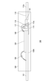
- FIG. 3 is a top view showing an example of the current sensor 100;
- FIG. FIG. 1B is a JJ′ cross-sectional view of the current sensor 100 shown in FIG. 1A.
- 3 is a diagram showing an example of functional blocks of a current sensor 100 including a signal processing IC 120;
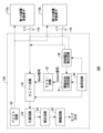
- FIG. 3 is a diagram showing an example of functional blocks of a current sensor 300 including a signal processing IC 120 according to the first embodiment;
- FIG. 3 is a diagram showing an example of a more specific circuit configuration of current sensor 300.
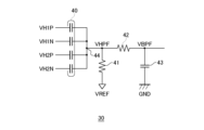
- FIG. 3 is a diagram showing an example of a specific circuit configuration of a common-mode voltage detection circuit 30;
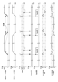
- FIG. 6 is a diagram showing an example of a specific operation of the current sensor 300 shown in FIGS. 3 and 5;
- FIG. 10 is a diagram showing an example of functional blocks of a current sensor 600 including a signal processing IC 120 according to a second embodiment
- FIG. 6 is a diagram showing an example of a more specific circuit configuration of current sensor 600.
- FIG. 9 is a diagram showing an example of a specific operation of current sensor 600 shown in FIGS. 7 and 8.
- FIG. 10 is a diagram showing an example of functional blocks of a current sensor 1000 including a signal processing IC 120 according to a third embodiment
- FIG. 11 is a diagram showing an example of functional blocks of a current sensor 1100 including a signal processing IC 120 according to a fourth embodiment;
- FIG. 1A is a top view showing an example of the current sensor 100.
- FIG. FIG. 1B is a JJ' cross-sectional view of the current sensor 100 shown in FIG. 1A.
- the current sensor 100 includes a conductor 110, a first magnetoelectric conversion element 113a, a second magnetoelectric conversion element 113b, a signal processing IC 120, and a metal plate .
- the conductor 110 has two lead terminals 112a and 112b.
- a current I to be measured flows through the conductor 110 .
- the conductor 110 has a U-shaped current path 111 through which the current I to be measured flows in the winding direction from the lead terminal 112a side to the lead terminal 112b side.
- a first magnetoelectric conversion element 113a is arranged in the gap 110a of the conductor 110 located inside the U-shaped current path 111 .
- a second magnetoelectric conversion element 113b is arranged with the current path 111 interposed therebetween.
- the first magnetoelectric conversion element 113a and the second magnetoelectric conversion element 113b are arranged to face each other via the conductor 110, and output a signal corresponding to the magnetic field.
- the signal processing IC 120 is supported by a metal plate 130 insulated from the conductor 110.
- the metal plate 130 includes a U-shaped portion, and the U-shaped portion of the current path 111 is arranged within the U-shaped portion of the metal plate 130 .
- a second magnetoelectric conversion element 113 b is arranged in the gap 110 b between the U-shaped portion of the current path 111 and the U-shaped portion of the metal plate 130 .
- the first magnetoelectric conversion element 113a and the second magnetoelectric conversion element 113b may be, for example, Hall elements, magnetoresistive effect elements, Hall ICs, and magnetoresistive effect ICs.
- Mold resin 180 is mold resin such as epoxy resin.
- the first magnetoelectric conversion element 113a is arranged in the gap 110a near the U-shaped portion of the current path 111. As shown in FIG. Therefore, the first magnetoelectric conversion element 113 a detects the magnetic flux density generated by the current I to be measured flowing through the conductor 110 and outputs an electric signal corresponding to the magnetic flux density to the signal processing IC 120 .
- the second magnetoelectric conversion element 113b also detects the magnetic flux density generated by the current I to be measured flowing through the conductor 110 and outputs an electrical signal corresponding to the magnetic flux density to the signal processing IC 120. In this manner, the first magnetoelectric conversion element 113a and the second magnetoelectric conversion element 113b detect the current according to the measured current I flowing through the conductor 110.
- the first magneto-electric conversion element 113a and the second magneto-electric conversion element 113b are separated from the conductor 110 by gaps 110a and 110b, respectively, and are in a state of not contacting the conductor 110 at all times. Thereby, there is no electrical continuity between the conductor 110 and the first magnetoelectric conversion element 113a and between the conductor 110 and the second magnetoelectric conversion element 113b. is ensured. Also, the first magnetoelectric conversion element 113a is supported by an insulating member 114 indicated by a dashed line in FIG. 1A.
- the insulating member 114 may be, for example, an insulating tape made of a polyimide material having a high withstand voltage.
- the first magnetoelectric conversion element 113a and the second magnetoelectric conversion element 113b are electrically connected to the signal processing IC 120 via wires 160, which are conductive wires such as metal wires.
- the signal processing IC 120 is electrically connected to lead terminals 141 via wires 150, which are conductive wires such as metal wires.
- the signal processing IC 120 may be composed of, for example, an LSI (Large Scale Integration).
- the signal processing IC 120 includes, for example, a memory, processor, bias circuit, subtraction circuit, correction circuit, amplifier circuit, and the like. The configuration of the signal processing IC 120 is shown in a detailed functional block diagram in FIG. 2, which will be described later.
- the insulating member 114 is joined to a portion of the back surface 130A of the metal plate 130 to support the first magnetoelectric conversion element 113a. be done. Although only the first magnetoelectric transducer 113a is shown in FIG. 1B, the insulating member 114 supports the second magnetoelectric transducer 113b as well as the first magnetoelectric transducer 113a.
- a step 101 is formed on the back surface of part of the conductor 110 , and the step 101 keeps the conductor 110 from contacting the insulating member 114 at all times.
- a mold resin 180 is filled between the back surface of the conductor 110 and the insulating member 114 .
- the insulating member 114 is made of, for example, an insulating tape made of a polyimide material having excellent pressure resistance, and is attached to the back surface 130A of the metal plate 130 in the state shown in FIG. 1B to support the first magnetoelectric conversion element 113a from the back surface. .
- the conductor 110 and the first magnetoelectric conversion element 113a are provided on the same surface of the insulating member 114. As shown in FIG. Further, the height position of the magneto-sensitive surface 116 of the first magnetoelectric conversion element 113a is arranged between the heights from the bottom surface to the top surface of the conductor 110, for example, in the center.
- the first magnetoelectric conversion element 113a and the second magnetoelectric conversion element 113b are electrically connected to the signal processing IC 120 via wires 160, which are conductive wires such as metal wires. However, due to the structure described above, conductor 110 and wire 160 are electrically joined by parasitic capacitance 117 .
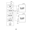
- FIG. 2 is a diagram showing an example of functional blocks of the current sensor 100 including the signal processing IC 120.
- the signal processing IC 120 includes a bias circuit 22 , a subtraction circuit 23 , a correction circuit 24 and an amplifier circuit 25 .
- the bias circuit 22 is connected to the first magnetoelectric conversion element 113a and the second magnetoelectric conversion element 113b, and supplies power to the first magnetoelectric conversion element 113a and the second magnetoelectric conversion element 113b. In other words, the bias circuit 22 applies (flows) an excitation current to the first magnetoelectric conversion element 113a and the second magnetoelectric conversion element 113b.
- the subtraction circuit 23 cancels the influence of the magnetic field generated outside based on the difference between the output of the first magnetoelectric conversion element 113a and the output of the second magnetoelectric conversion element 113b. Calculate the current value. Also, a transient high voltage (dvdt) is applied to conductor 110 and voltage noise propagating through parasitic capacitance 117 is similarly canceled.
- dvdt transient high voltage
- the correction circuit 24 corrects the output value from the subtraction circuit 23. For example, the correction circuit 24 corrects the output values of the first magnetoelectric conversion element 113a and the second magnetoelectric conversion element 113b based on the operating temperature and according to temperature correction coefficients stored in advance in the memory. The correction circuit 24 may perform offset correction based on the absolute value of the zero current voltage (open circuit voltage (OCV)) of the current sensor 100 and offset correction due to temperature drift.
- OCV open circuit voltage
- the amplifier circuit 25 amplifies the output value from the correction circuit 24 .
- the current sensor 100 configured as described above calculates the current value based on the difference between the outputs of the first magnetoelectric conversion element 113a and the second magnetoelectric conversion element 113b, the influence of the magnetic field generated outside can be canceled. . That is, according to the current sensor 100 configured as described above, in an ideal case, the effect of applying a transient high voltage (dvdt) to the conductor 110 is invisible. However, if there is wire flow during filling of the mold resin or deviation during assembly, the balance of the parasitic capacitance 117 is lost, and the propagating voltage noise is amplified and output without being canceled. .
- FIG. 3 shows an example of functional blocks of a current sensor 300 including the signal processing IC 120 according to the first embodiment.
- FIG. 4 is a diagram showing an example of a more specific circuit configuration of current sensor 300.
- the signal processing IC 120 includes a bias circuit 22 , a subtraction circuit 23 , a correction circuit 24 and an amplifier circuit 25 .
- the signal processing IC 120 further includes a common-mode voltage detection circuit 30, a threshold determination comparison circuit 31, a timer circuit 32, a select circuit 33, and a reference circuit .
- the signal processing IC 120 is an example of a signal processing section.
- the common-mode voltage detection circuit 30 is connected to the pair of first output terminals of the first magnetoelectric conversion element 113a, the pair of second output terminals of the second magnetoelectric conversion element 113b, and the reference circuit .
- the common-mode voltage detection circuit 30 detects the voltage of the first signal output from each of the pair of first output terminals of the first magnetoelectric conversion element 113a and the voltage of each of the pair of second output terminals of the second magnetoelectric conversion element 113b. and the voltage of the second signal output from the combined common mode voltage is detected.
- the common-mode voltage detection circuit 30 detects and outputs a common-mode voltage obtained by synthesizing the voltages propagated through the parasitic capacitances 117 when a transient high voltage (dvdt) is applied to the conductor 110 .
- the subtraction circuit 23 calculates the amount of current flowing through the conductor 110 based on each first signal and each second signal. Derive the current value.
- the subtraction circuit 23 is an example of a derivation unit, and may be an addition circuit or a differential amplifier circuit depending on the number of sensors and arrangement of conductors.
- the subtraction circuit 23 When the common-mode voltage detected by the common-mode voltage detection circuit 30 exceeds the threshold voltage, the subtraction circuit 23 masks the respective first signals and the respective second signals so that they are different from the first signals and the second signals. It outputs a predetermined reference signal. The subtraction circuit 23 derives the current value of the current flowing through the conductor 110 based on the first signal and the second signal after the gain is lowered, as shown in a second embodiment described later. You may
- the subtraction circuit 23 outputs signals obtained by replacing the respective first signals and the respective second signals with predetermined signals for a predetermined period after the common-mode voltage exceeds a predetermined threshold voltage. good. As shown in a second embodiment described later, the subtraction circuit 23, after the common-mode voltage exceeds a predetermined threshold voltage and for a predetermined period, reduces the gain below a predetermined gain. Based on the one signal and each second signal, a current value of the current flowing through conductor 110 may be derived.
- FIG. 5 is a diagram showing an example of a specific circuit configuration of the common-mode voltage detection circuit 30.
- a signal of voltage VH1P and a signal of voltage VH1N are output from a pair of first output terminals of the first magnetoelectric conversion element 113a.
- the signal of voltage VH1P and the signal of voltage VH1N are examples of the first signal.
- a signal of voltage VH2P and a signal of voltage VH2N are output from a pair of second output terminals of the second magnetoelectric conversion element 113b.
- the signal of voltage VH2P and the signal of voltage VH2N are examples of the second signal.
- Each of the pair of first output terminals and the pair of second output terminals is electrically connected to one end of each detection capacitor 40 .
- Each sensing capacitor 40 has the same capacitance.
- the other end of each detection capacitor 40 is electrically connected to a common node 44 .
- the detection capacitor 40 is an example of a first capacitor and a second capacitor.
- each detection capacitor 40 is connected to one end of resistor 41 via node 44 .
- the other end of the resistor 41 is connected to the reference circuit 34 and applied with the reference voltage VREF.
- One end of the resistor 41 is also connected to one end of the resistor 42 .
- One end of the capacitor 43 is connected to the other end of the resistor 42 .
- the other end of capacitor 43 is grounded.
- the capacity 43 is an example of a third capacity.
- a resistor 41 is connected between a node 44 to which the other end of each detection capacitor 40 is connected and the output terminal of the reference circuit 34 that outputs the reference voltage VREF.
- the common-mode voltage detection circuit 30 has a function of detecting a common-mode voltage.
- the changing voltage excited according to the current I to be measured flowing through the conductor 110 is the differential output ⁇ V1 of the first magnetoelectric conversion element 113a and the differential output ⁇ V1 of the second magnetoelectric conversion element 113b. is ⁇ V2, it is represented by the following equation.
- VH1P ⁇ V1/2 (3)
- VH1N - ⁇ V1/2 (4)
- VH2P - ⁇ V2/2 (5)
- VH2N ⁇ V2/2 (6)
- the changing voltage excited according to the current I to be measured becomes 0 and is not output.
- VH1P, VH1N, VH2P, and VH2N are expressed by the following equations.
- VH1P ⁇ Vd (8)
- VH1N ⁇ Vd (9)
- VH2P ⁇ Vd (10)
- VH2N ⁇ Vd (11)
- the common-mode voltage detection circuit 30 can detect only a transient high voltage (dvdt).
- the common-mode voltage detection circuit 30 can perform similar detection even when a pair of output terminals VH1P and VH1N are used.
- the signal processing IC 120 selects any two terminals from the pair of first output terminals of the first magnetoelectric conversion element 113a and the pair of second output terminals of the second magnetoelectric conversion element 113b, VH1P, VH1N, VH2P, and VH2N.
- the signal processing IC 120 generates a changing voltage excited according to the current I to be measured due to the positional relationship between the conductor 110 and the first magnetoelectric conversion element 113a and the second magnetoelectric conversion element 113b. It is also possible to select any combination that results in zero.
- the integrating circuit Configured. Unintended high-frequency noise can be removed by configuring such an integration circuit.
- FIG. 4 describes an example of configuring a low-pass filter using an integrating circuit
- the integrating circuit may not be used.
- another filter with arbitrary frequency characteristics may be used.
- the threshold judgment comparison circuit 31 is connected to the common-mode voltage detection circuit 30 and connected to the reference circuit 34 .
- a voltage of VREF ⁇ V is supplied to the threshold judgment comparison circuit 31 with respect to the reference voltage VREF supplied to the common-mode voltage detection circuit 30, and the threshold judgment comparison circuit 31 uses a general window comparator circuit to obtain
- the timer circuit 32 is connected to the threshold judgment/comparison circuit 31 and counts at an arbitrary CLK although not explicitly shown in FIG.
- the timer circuit 32 receives the first Detect signal from the threshold judgment comparison circuit 31, changes the Mask signal, which is an output signal, from Low level to High level, and maintains the High level time for a predetermined count number. After that, the Mask signal is changed from High level to Low level.
- the timer circuit 32 does not accept the second and subsequent Detect signals for a certain period of time. That is, the timer circuit 32 does not accept the Low signal for a certain period of time, and after that, at an arbitrary time, the timer circuit 32 is initialized and performs the operation of accepting the next Detect signal.
- the timer circuit 32 receives the first Detect signal from the threshold judgment comparison circuit 31 and changes the Mask signal, which is an output signal, from Low level to High level. Further, the timer circuit 32 receives the second Detect signal, changes the Mask signal from High level to Low level, and does not accept the third and subsequent Detect signals for a certain period of time. Thereafter, at an arbitrary time, the timer circuit 32 is initialized and performs an operation of accepting the next Detect signal. By operating in this manner, timer circuit 32 detects that a transient high voltage (dvdt) has been applied to conductor 110, and a predetermined time period has passed since the transient high voltage was applied. Alternatively, the Mask signal can be generated only during the time when the high voltage is applied.
- dvdt transient high voltage
- the Mask signal can be generated only during the time when the high voltage is applied.
- the select circuit 33 is connected to the pair of first output terminals of the first magnetoelectric conversion element 113a, the pair of second output terminals of the second magnetoelectric conversion element 113b, the reference circuit 34, and the timer circuit 32.
- the select circuit 33 selects the output from the pair of first output terminals of the first magnetoelectric conversion element 113a and the pair of second output terminals of the second magnetoelectric conversion element 113b. Output.
- the select circuit 33 controls the pair of first output terminals of the first magnetoelectric conversion element 113a and the second magnetoelectric conversion element 113b to suppress peaks in the sensor output.
- the correction circuit 24 corrects the output value from the subtraction circuit 23.
- the correction circuit 24 corrects the output values of the first magnetoelectric conversion element 113a and the second magnetoelectric conversion element 113b based on the operating temperature, for example, according to temperature correction coefficients stored in advance in the memory.
- the amplifier circuit 25 amplifies the output value from the correction circuit 24 .
- the bias circuit 22 is a circuit that supplies current or voltage to the first magnetoelectric conversion element 113a and the second magnetoelectric conversion element 113b, and the chopper switch 21 drives the first magnetoelectric conversion element 113a.
- a pair of input terminals for supplying current, a pair of first output terminals, and a pair of input terminals for supplying drive current to the second magnetoelectric transducer 113b and a pair of second output terminals are switched to drive the chopper. do.
- FIG. 6 shows an example of specific operations of the current sensor 300 shown in FIGS.
- a transient high voltage (dvdt) is input to the conductor 110 in addition to the input current
- the peak of the sensor output is suppressed as shown by the dashed line.
- the solid line of the sensor output (corresponding to ⁇ I) is the sensor output waveform when the Mask signal is not used, and the broken line is the sensor output waveform when the Mask signal is used.
- FIG. 7 is a diagram showing an example of functional blocks of a current sensor 600 including a signal processing IC 120 according to the second embodiment.
- FIG. 8 is a diagram showing an example of a more specific circuit configuration of current sensor 600. As shown in FIG. Since the current sensor 600 according to the second embodiment has the same functional blocks as the current sensor 300 according to the first embodiment, some of the same functional parts will be omitted.
- the timer circuit 32 is connected to the threshold judgment/comparison circuit 31 and to a subtraction circuit 63 having a gain adjusting function.
- the output signal from timer circuit 32 is generated in the same manner as in the first embodiment. However, although the output signal from the timer circuit 32 was used as the Mask signal in the first embodiment, it is used as the Adjust signal for gain adjustment in the second embodiment.
- the subtraction circuit 63 is connected to the pair of first output terminals of the first magnetoelectric conversion element 113a, the pair of second output terminals of the second magnetoelectric conversion element 113b, and the timer circuit 32.
- the subtraction circuit 63 calculates the influence of the magnetic field generated outside based on the difference between the output of the first magnetoelectric conversion element 113a and the output of the second magnetoelectric conversion element 113b.
- the current value is calculated by canceling (offsetting in-phase noise).
- the subtraction circuit 63 when it receives a High level Adjust signal, it shifts to a predetermined gain and calculates a current value.
- the gain to be fixed may be a gain setting selected from the total gain range required for the signal processing IC 120, or may be a separately prepared gain setting outside the range. In any case, in order to suppress the peak of the sensor output, it is desirable to lower the gain when the Adjust signal is at High level than when the Adjust signal is at Low level.
- the amplifier circuit 25 may receive the Adjust signal and adjust the gain.
- FIG. 9 shows an example of specific operation of the current sensor 600 shown in FIGS.
- An example is shown in which the gain is set to 1/2 when the Adjust signal is at High level.
- the Adjust signal is not used, there is a concern that when a transient high voltage (dvdt) is input, it will exceed the voltage (long two-dot chain line) that is allowed as a sensor output.
- the peak of the sensor output is suppressed as shown by the dashed line.
- the solid line of the sensor output (corresponding to ⁇ I) is the sensor output waveform when the Adjust signal is not used, and the broken line is the sensor output waveform when the Adjust signal is used.
- Adjust signal When the Adjust signal is not used, when a transient high voltage (dvdt) is input, it is superimposed on the sensor output that responds to the current, resulting in a complex sensor output waveform, and the allowable voltage (long two-dot chain line) is concerned about exceeding.
- the Adjust signal When the Adjust signal is used, it becomes like the broken line, the sensor output responds to the current equivalent to 1/2, and the peak is suppressed.
- the current sensor 600 according to the second embodiment by lowering the gain within a range where there is no influence, it is possible to accelerate the return to operation after applying a transient high voltage (dvdt). Further, according to the current sensor 600 according to the second embodiment, unlike the current sensor 300 according to the first embodiment, it is not necessary to switch the input using a switch or the like by the select circuit 33, and continuous operation can be performed. . Fluctuation of circuit operating point is small. From the above, the current sensor 600 according to the second embodiment can accelerate recovery more than the current sensor 300 according to the first embodiment.
- FIG. 10 shows an example of functional blocks of a current sensor 1000 including a signal processing IC 120 according to the third embodiment.
- This embodiment does not use the second magnetoelectric conversion element 113b of FIG. Since the current sensor 1000 according to the third embodiment has the same functional blocks as the current sensor 300 according to the first embodiment, some of the same functional parts will be omitted.
- the common-mode voltage detection circuit 30 is connected to a pair of output terminals of the first magnetoelectric conversion element 113a, and as described above, it is clear that similar detection can be performed even when a pair of output terminals VH1P and VH1N are used. be.
- FIG. 11 shows an example of functional blocks of a current sensor 1100 including a signal processing IC 120 according to the fourth embodiment. This is an embodiment that does not use the second magnetoelectric conversion element 113b of FIG. Since the current sensor 1100 according to the third embodiment has the same functional blocks as the current sensor 600 according to the second embodiment, some of the same functional parts will be omitted.
- the differential amplifier circuit 113 is connected to a pair of output terminals of the first magnetoelectric conversion element 113a, and when receiving a High level Adjust signal, shifts to a predetermined gain and calculates a current value.
- the predetermined gain may be set to a gain selected from within the total gain range required for the signal processing IC 120, or may be set to a separately prepared gain outside the range. In any case, in order to suppress the peak of the sensor output, it is desirable to lower the gain when the Adjust signal is at High level than when the Adjust signal is at Low level.
- the amplifier circuit 25 may receive the Adjust signal and adjust the gain.
- the current sensor 1000 according to the third embodiment and the current sensor 1100 according to the fourth embodiment when the disturbance magnetic field can be suppressed by a mechanism such as an installation location where the influence of the disturbance magnetic field is small, or a magnetic shield, Since there is no need to use a plurality of magnetoelectric conversion elements and a differential amplifier circuit can be used instead of a subtraction circuit, related circuits can be reduced, current consumption can be reduced, and die cost can be reduced.
Landscapes
- Physics & Mathematics (AREA)
- General Physics & Mathematics (AREA)
- Engineering & Computer Science (AREA)
- Power Engineering (AREA)
- Measuring Magnetic Variables (AREA)
Priority Applications (4)
| Application Number | Priority Date | Filing Date | Title |
|---|---|---|---|
| JP2024504656A JP7703772B2 (ja) | 2022-03-03 | 2023-02-24 | 電流センサ、及び電流検出方法 |
| DE112023001219.9T DE112023001219T5 (de) | 2022-03-03 | 2023-02-24 | Stromsensor und Stromerkennungsverfahren |
| CN202380024698.8A CN118891529A (zh) | 2022-03-03 | 2023-02-24 | 电流传感器以及电流检测方法 |
| US18/822,313 US20240418752A1 (en) | 2022-03-03 | 2024-09-02 | Current sensor and current detection method |
Applications Claiming Priority (2)
| Application Number | Priority Date | Filing Date | Title |
|---|---|---|---|
| JP2022-033016 | 2022-03-03 | ||
| JP2022033016 | 2022-03-03 |
Related Child Applications (1)
| Application Number | Title | Priority Date | Filing Date |
|---|---|---|---|
| US18/822,313 Continuation US20240418752A1 (en) | 2022-03-03 | 2024-09-02 | Current sensor and current detection method |
Publications (1)
| Publication Number | Publication Date |
|---|---|
| WO2023167096A1 true WO2023167096A1 (ja) | 2023-09-07 |
Family
ID=87883636
Family Applications (1)
| Application Number | Title | Priority Date | Filing Date |
|---|---|---|---|
| PCT/JP2023/006676 Ceased WO2023167096A1 (ja) | 2022-03-03 | 2023-02-24 | 電流センサ、及び電流検出方法 |
Country Status (5)
| Country | Link |
|---|---|
| US (1) | US20240418752A1 (https=) |
| JP (1) | JP7703772B2 (https=) |
| CN (1) | CN118891529A (https=) |
| DE (1) | DE112023001219T5 (https=) |
| WO (1) | WO2023167096A1 (https=) |
Citations (8)
| Publication number | Priority date | Publication date | Assignee | Title |
|---|---|---|---|---|
| JP2011146904A (ja) * | 2010-01-14 | 2011-07-28 | Renesas Electronics Corp | 受信回路 |
| JP2013531938A (ja) * | 2010-05-28 | 2013-08-08 | ザイリンクス インコーポレイテッド | 広いコモンモード入力範囲を有する差動比較回路 |
| JP2015045640A (ja) * | 2013-08-15 | 2015-03-12 | リニアー テクノロジー コーポレイションLinear Technology Corporation | 電流センス回路、およびモータの巻線を駆動するための回路 |
| WO2016047149A1 (ja) * | 2014-09-26 | 2016-03-31 | 旭化成エレクトロニクス株式会社 | ホール起電力信号検出回路及び電流センサ |
| JP6321800B2 (ja) * | 2014-06-27 | 2018-05-09 | 旭化成エレクトロニクス株式会社 | 電流センサ |
| CN111200402A (zh) * | 2020-02-19 | 2020-05-26 | 电子科技大学 | 一种能够提升增益的高线性度动态残差放大器电路 |
| US20200186102A1 (en) * | 2018-12-05 | 2020-06-11 | Bae Systems Information And Electronic Systems Integration Inc. | Dynamic differential amplifier with enhanced gain |
| JP2021036198A (ja) * | 2017-10-04 | 2021-03-04 | 株式会社村田製作所 | 電流センサの製造方法および電流センサ |
Family Cites Families (17)
| Publication number | Priority date | Publication date | Assignee | Title |
|---|---|---|---|---|
| JPS6321800U (https=) | 1986-07-28 | 1988-02-13 | ||
| JP3774604B2 (ja) * | 1999-12-27 | 2006-05-17 | 三菱電機株式会社 | ガス絶縁開閉装置 |
| US7852090B2 (en) * | 2007-10-01 | 2010-12-14 | Echostar Technologies L.L.C. | Apparatus, system and methods for ground current detection |
| JP5625316B2 (ja) * | 2009-10-22 | 2014-11-19 | 株式会社オートネットワーク技術研究所 | 電気接続箱 |
| GB0919969D0 (en) * | 2009-11-14 | 2009-12-30 | Gigle Semiconductor Ltd | Current measuring apparatus |
| JP5724660B2 (ja) * | 2011-06-15 | 2015-05-27 | 株式会社オートネットワーク技術研究所 | 電流検出装置 |
| US9945692B2 (en) * | 2013-04-29 | 2018-04-17 | Massachusetts Institute Of Technology | Non-intrusive monitoring |
| CA2868663C (en) * | 2013-10-21 | 2016-11-08 | Tomasz Barczyk | Methods and systems relating to ac current measurements |
| JP2015194472A (ja) * | 2014-01-23 | 2015-11-05 | 株式会社デンソー | 電流検出システム |
| JP6190537B2 (ja) * | 2014-08-05 | 2017-08-30 | アルプス電気株式会社 | 電流センサ |
| US20170184635A1 (en) * | 2015-12-28 | 2017-06-29 | Everspin Technologies, Inc. | Sensing apparatus for sensing current through a conductor and methods therefor |
| WO2018092336A1 (ja) * | 2016-11-17 | 2018-05-24 | 株式会社村田製作所 | 電流センサ |
| EP3671228B1 (en) * | 2018-12-12 | 2023-03-29 | Melexis Technologies SA | Current sensor with integrated current conductor |
| JP2020095029A (ja) * | 2018-12-12 | 2020-06-18 | メレキシス テクノロジーズ エス エーMelexis Technologies SA | 電流センサ |
| CN112114180B (zh) * | 2019-06-20 | 2024-04-26 | 株式会社电装 | 电力转换装置 |
| US12212137B2 (en) * | 2022-01-04 | 2025-01-28 | Solaredge Technologies Ltd. | System and methods for regulating connections of loads to a network |
| JP2024147280A (ja) * | 2023-04-03 | 2024-10-16 | 足立建設工業株式会社 | 充填装置 |
-
2023
- 2023-02-24 DE DE112023001219.9T patent/DE112023001219T5/de active Pending
- 2023-02-24 WO PCT/JP2023/006676 patent/WO2023167096A1/ja not_active Ceased
- 2023-02-24 CN CN202380024698.8A patent/CN118891529A/zh active Pending
- 2023-02-24 JP JP2024504656A patent/JP7703772B2/ja active Active
-
2024
- 2024-09-02 US US18/822,313 patent/US20240418752A1/en active Pending
Patent Citations (8)
| Publication number | Priority date | Publication date | Assignee | Title |
|---|---|---|---|---|
| JP2011146904A (ja) * | 2010-01-14 | 2011-07-28 | Renesas Electronics Corp | 受信回路 |
| JP2013531938A (ja) * | 2010-05-28 | 2013-08-08 | ザイリンクス インコーポレイテッド | 広いコモンモード入力範囲を有する差動比較回路 |
| JP2015045640A (ja) * | 2013-08-15 | 2015-03-12 | リニアー テクノロジー コーポレイションLinear Technology Corporation | 電流センス回路、およびモータの巻線を駆動するための回路 |
| JP6321800B2 (ja) * | 2014-06-27 | 2018-05-09 | 旭化成エレクトロニクス株式会社 | 電流センサ |
| WO2016047149A1 (ja) * | 2014-09-26 | 2016-03-31 | 旭化成エレクトロニクス株式会社 | ホール起電力信号検出回路及び電流センサ |
| JP2021036198A (ja) * | 2017-10-04 | 2021-03-04 | 株式会社村田製作所 | 電流センサの製造方法および電流センサ |
| US20200186102A1 (en) * | 2018-12-05 | 2020-06-11 | Bae Systems Information And Electronic Systems Integration Inc. | Dynamic differential amplifier with enhanced gain |
| CN111200402A (zh) * | 2020-02-19 | 2020-05-26 | 电子科技大学 | 一种能够提升增益的高线性度动态残差放大器电路 |
Also Published As
| Publication number | Publication date |
|---|---|
| JPWO2023167096A1 (https=) | 2023-09-07 |
| DE112023001219T5 (de) | 2025-01-16 |
| JP7703772B2 (ja) | 2025-07-07 |
| CN118891529A (zh) | 2024-11-01 |
| US20240418752A1 (en) | 2024-12-19 |
Similar Documents
| Publication | Publication Date | Title |
|---|---|---|
| US9983273B2 (en) | Magnetic field detecting sensor and magnetic field detecting apparatus using the same | |
| EP1965217B1 (en) | High bandwidth open-loop current sensor | |
| US7605580B2 (en) | Integrated hybrid current sensor | |
| US10215779B2 (en) | Non-contact voltage measurement device | |
| US10317439B2 (en) | Current sensor, system and method | |
| US11789095B2 (en) | Current sensor, magnetic sensor and circuit | |
| US10429221B2 (en) | Electromagnetic flowmeter | |
| JP2008513762A (ja) | 連続校正式磁界センサー | |
| CN101114540A (zh) | 线圈组及使用该线圈组的电子装置 | |
| US8525529B2 (en) | Impedance detection circuit and adjustment method of impedance detection circuit | |
| JP6564528B2 (ja) | 磁気イメージセンサー | |
| JP2008298761A (ja) | 電流センサ | |
| WO2023167096A1 (ja) | 電流センサ、及び電流検出方法 | |
| JP7731898B2 (ja) | 電流変換器 | |
| JPWO2023167096A5 (https=) | ||
| CN102971634B (zh) | 确定测量信道的修正参数和检测电动机的端子电压的方法或电压检测系统 | |
| US20240027496A1 (en) | Amplifier circuit and measurement apparatus | |
| JP5730697B2 (ja) | イオンセンシング装置およびイオン発生器 | |
| JP7803433B2 (ja) | 電流センサ | |
| JP7492445B2 (ja) | モータ制御装置 | |
| JP2024055404A (ja) | 半導体集積回路 | |
| JP2009047447A (ja) | 物理量センサ | |
| JP2026045277A (ja) | 処理回路、電流センサ、および処理方法 | |
| JP2003149309A (ja) | 多チャンネル形磁気検出装置 | |
| JP2003294783A (ja) | 加速度センサ |
Legal Events
| Date | Code | Title | Description |
|---|---|---|---|
| 121 | Ep: the epo has been informed by wipo that ep was designated in this application |
Ref document number: 23763355 Country of ref document: EP Kind code of ref document: A1 |
|
| ENP | Entry into the national phase |
Ref document number: 2024504656 Country of ref document: JP Kind code of ref document: A |
|
| WWE | Wipo information: entry into national phase |
Ref document number: 202380024698.8 Country of ref document: CN |
|
| WWE | Wipo information: entry into national phase |
Ref document number: 112023001219 Country of ref document: DE |
|
| 122 | Ep: pct application non-entry in european phase |
Ref document number: 23763355 Country of ref document: EP Kind code of ref document: A1 |