WO2023157291A1 - Appareil et procédé d'inspection de dispositifs - Google Patents
Appareil et procédé d'inspection de dispositifs Download PDFInfo
- Publication number
- WO2023157291A1 WO2023157291A1 PCT/JP2022/006941 JP2022006941W WO2023157291A1 WO 2023157291 A1 WO2023157291 A1 WO 2023157291A1 JP 2022006941 W JP2022006941 W JP 2022006941W WO 2023157291 A1 WO2023157291 A1 WO 2023157291A1
- Authority
- WO
- WIPO (PCT)
- Prior art keywords
- inspection
- semiconductor device
- probe head
- unit
- result
- Prior art date
Links
- 238000007689 inspection Methods 0.000 title claims abstract description 409
- 238000000034 method Methods 0.000 title claims description 83
- 239000000523 sample Substances 0.000 claims abstract description 231
- 239000004065 semiconductor Substances 0.000 claims abstract description 163
- 238000004458 analytical method Methods 0.000 claims abstract description 76
- 230000002159 abnormal effect Effects 0.000 claims abstract description 34
- 238000012545 processing Methods 0.000 claims abstract description 26
- 230000005856 abnormality Effects 0.000 claims description 71
- 230000002950 deficient Effects 0.000 claims description 63
- 238000012360 testing method Methods 0.000 claims description 30
- 238000010586 diagram Methods 0.000 description 21
- 230000007246 mechanism Effects 0.000 description 14
- 230000006870 function Effects 0.000 description 7
- 230000015654 memory Effects 0.000 description 5
- 230000008569 process Effects 0.000 description 5
- 239000000758 substrate Substances 0.000 description 4
- 238000000540 analysis of variance Methods 0.000 description 3
- 230000007257 malfunction Effects 0.000 description 3
- 239000004593 Epoxy Substances 0.000 description 2
- 238000005516 engineering process Methods 0.000 description 2
- 239000011521 glass Substances 0.000 description 2
- 239000013598 vector Substances 0.000 description 2
- 238000005452 bending Methods 0.000 description 1
- 238000004364 calculation method Methods 0.000 description 1
- 239000003990 capacitor Substances 0.000 description 1
- 230000008859 change Effects 0.000 description 1
- 238000004140 cleaning Methods 0.000 description 1
- 230000007547 defect Effects 0.000 description 1
- 238000001514 detection method Methods 0.000 description 1
- 238000000605 extraction Methods 0.000 description 1
- 238000012423 maintenance Methods 0.000 description 1
- 238000005259 measurement Methods 0.000 description 1
- 230000004048 modification Effects 0.000 description 1
- 238000012986 modification Methods 0.000 description 1
- 230000008439 repair process Effects 0.000 description 1
- 230000000717 retained effect Effects 0.000 description 1
- 230000003068 static effect Effects 0.000 description 1
- 238000010998 test method Methods 0.000 description 1
Images


Classifications
-
- H—ELECTRICITY
- H01—ELECTRIC ELEMENTS
- H01L—SEMICONDUCTOR DEVICES NOT COVERED BY CLASS H10
- H01L22/00—Testing or measuring during manufacture or treatment; Reliability measurements, i.e. testing of parts without further processing to modify the parts as such; Structural arrangements therefor
Definitions
- This application relates to a device inspection apparatus and a device inspection method.
- Japanese Unexamined Patent Application Publication No. 2002-100001 discloses a prober device and a semiconductor device inspection method for inspecting a plurality of chips formed on a semiconductor wafer in parallel in a wafer state. As the number of chips to be inspected increases, the contact resistance between the probe block and the electrodes of the chip increases, resulting in erroneous determination of defective products.
- the semiconductor device inspection method using the prober device of Patent Document 1 as the number of chips to be inspected increases, chips that have been erroneously determined to be defective are reinspected, so that chips to be reinspected are selected. a step of cleaning a plurality of probe blocks; and a step of selecting one probe block to be used for retesting from the plurality of probe blocks used in parallel testing of a plurality of chips.
- the device inspection which inspects the electrical characteristics, etc. of the semiconductor device to be inspected, is not limited to the wafer state, but may be performed in the separated chip state.
- Device inspection for inspecting an object to be inspected includes a method of inspecting by bringing electrodes of the object to be inspected into contact with a plurality of probes attached to a probe head.
- the probe head has a plurality of probes and corresponds to the probe block of Patent Document 1.
- an abnormality occurs in the probe that causes contact failure between the inspection object and the probe.
- a non-defective product is erroneously determined as a defective product.
- the non-defective product rate for each probe block is calculated based on the inspection results read after all the chips on the wafer have been inspected. Abnormalities in the probe block (probe head) cannot be detected in the first inspection.
- the technology disclosed in the specification of the present application aims to detect an abnormality of the probe head together with the result of the inspection target when the inspection of the device to be inspected ends.
- An example device inspection apparatus disclosed in the specification of the present application includes a housing for mounting a plurality of semiconductor devices, a plurality of probe heads that have probes that contact electrodes of the semiconductor devices, and is used individually for each semiconductor device, An inspection unit that applies an electrical signal for each semiconductor device to a plurality of semiconductor devices and measures inspection value data for each semiconductor device, and an inspection judgment that determines whether the semiconductor device is a non-defective product or a defective product based on the inspection value data. and An example of the device inspection apparatus disclosed in the present specification further includes a storage unit for storing inspection result data including inspection value data and semiconductor device judgment results, and each inspection item stored in the storage unit.
- Analysis unit that analyzes whether there is a significant difference between multiple inspection result data for each probe head by statistical processing based on multiple inspection result data, and determines that the probe head is abnormal when there is a significant difference and a warning unit that indicates the result of abnormality determination that the probe head is abnormal in the analysis unit.
- An example device inspection apparatus disclosed in the present specification analyzes whether there is a significant difference between a plurality of inspection result data for each probe head by statistical processing based on a plurality of inspection result data stored in a storage unit. Therefore, it is possible to detect an abnormality of the probe head together with the result of the inspection target at the end of the inspection of the device to be inspected.
- FIG. 1 is a diagram showing the configuration of a device inspection apparatus according to Embodiment 1;
- FIG. 2 is a diagram showing an inspection target and a probe head mounted on the housing of FIG. 1;
- FIG. 3 is a diagram showing the probe head of FIG. 2 and an object to be inspected;
- FIG. 3 is a diagram showing a moving mechanism of the probe head of FIG. 2;
- FIG. FIG. 5 is a diagram showing an example of inspection results according to Embodiment 1;
- FIG. FIG. 5 is a diagram showing an example of inspection results according to Embodiment 1;
- FIG. FIG. 5 is a diagram showing an example of inspection results according to Embodiment 1;
- FIG. FIG. 5 is a diagram showing an example of inspection results according to Embodiment 1;
- FIG. FIG. 5 is a diagram showing an example of inspection results according to Embodiment 1;
- FIG. 5 is a diagram showing an example of inspection results according to Embodiment 1;
- FIG. 5 is
- FIG. 4 is a flowchart showing a device inspection method according to Embodiment 1; 2 is a diagram showing a hardware configuration example that implements the functions of a control unit, an inspection determination unit, and an analysis unit in FIG. 1; FIG. FIG. 10 is a diagram showing the configuration of a device inspection apparatus according to Embodiment 2; FIG. 10 is a diagram showing an example of inspection results according to Embodiment 2; FIG. 10 is a diagram showing the configuration of a device inspection apparatus according to Embodiment 3;
- FIG. 1 is a diagram showing the configuration of a device inspection apparatus according to Embodiment 1.
- FIG. FIG. 2 is a diagram showing the test object and the probe head mounted on the housing of FIG. 1
- FIG. 3 is a diagram showing the probe head and the test object of FIG. 4 is a diagram showing a moving mechanism of the probe head of FIG. 2.
- FIG. 5 to 8 are diagrams showing examples of inspection results according to the first embodiment, respectively.
- FIG. 9 is a flow chart showing the device inspection method according to the first embodiment
- FIG. 10 is a diagram showing a hardware configuration example realizing the functions of the control unit, inspection determination unit, and analysis unit shown in FIG.
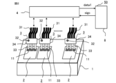
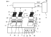
- a device inspection apparatus 50 of Embodiment 1 has a housing 1 for mounting a semiconductor device 2 to be inspected, a plurality of probes 33 , and at least one probe head 3 and an electrical signal to the semiconductor device 2 .
- An inspection unit 4 that measures inspection value data data1 of the semiconductor device 2 by applying voltage, a computer 8 that controls the inspection unit 4 and performs non-defective determination of the semiconductor device 2 and abnormality determination of the probe head 3, and abnormality determination of the probe head 3.
- a warning unit 41 for indicating a result, a moving mechanism 20 for moving the probe head 3, and an operation unit 5 for operating the computer 8 and the moving mechanism 20 are provided.
- the operation unit 5 is, for example, a touch panel display.
- FIG. 2 shows an example of a device inspection apparatus 50 that inspects a plurality of semiconductor devices 2 in parallel.
- FIG. 4 shows the moving mechanism 20 in the device inspection apparatus 50 when inspecting three semiconductor devices 2 in parallel.
- the moving mechanism 20 includes an actuator 24 that moves the head fixing plate 21 to which the plurality of probe heads 3a, 3b, and 3c are fixed in the x direction parallel to the device mounting surface 25 of the housing 1, and the head fixing plate 21. It has an air cylinder 23 that moves in the y direction, which is the direction perpendicular to the device mounting surface 25 of the housing 1 .
- the y-direction is perpendicular to the x-direction.
- the moving mechanism 20 has an air cylinder fixing plate 22 to which an air cylinder 23 is fixed.
- the air cylinder 23 holds the head fixing plate 21 to which the plurality of probe heads 3a, 3b, and 3c are fixed and moves the head fixing plate 21 in the y direction.
- the air cylinder fixed plate 22 is moved in the x direction by an actuator 24 .
- the moving mechanism 20 in the device inspection apparatus 50 for inspecting N semiconductor devices 2 in parallel is also the same as the moving mechanism 20 shown in FIG. N probe heads 3 are fixed to the head fixing plate 21 .
- the semiconductor device 2 to be inspected is, for example, an infrared sensor.
- An infrared sensor is a module in which a plurality of components are mounted on a substrate such as a glass epoxy substrate.
- the infrared sensor includes an infrared sensor chip having a temperature sensor formed by a photodiode, a control circuit or control IC (Integrated Circuit) for controlling the infrared sensor chip, and electronic components such as a capacitor.
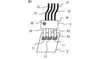
- 2 to 4 show only three of the plurality of electrodes 11 in the semiconductor device 2.
- the electrode 11 is, for example, an anode or cathode of a photodiode, an input/output electrode of a control circuit, or the like.
- the electrodes 11 of the semiconductor device 2 are formed on a substrate such as a glass epoxy substrate.
- the probe heads 3 and the semiconductor devices 2 to be inspected are in one-to-one correspondence, and the number of probe heads 3 and the number of semiconductor devices 2 to be inspected are the same.
- the probe head 3 includes a main body 34, a plurality of probes 33 fixed to the main body 34, and cables 31 connected to the plurality of probes 33, respectively. 2 to 4, since the light emitter 32 is provided on the main body 34 of the probe head 3, there is also a cable 31 for transmitting a signal for causing the light emitter 32 to emit light. Note that the number of cables 31 is not limited to the illustrated number.
- FIG. 4 shows a case in which there are three probe heads 3 and three semiconductor devices 2, and the three probe heads 3 are denoted by 3a, 3b, and 3c to distinguish them.
- reference numerals 2a, 2b, and 2c are attached to distinguish the three semiconductor devices 2, and reference numerals 32a, 32b, and 32c are attached to distinguish the three light emitters 32. . That is, the reference numerals for the probe heads are 3 in general, and 3a, 3b, and 3c when distinguishing them.
- the reference numerals for semiconductor devices are 2 in general, and 2a, 2b, and 2c when distinguishing them.
- the reference numerals for the light emitters are 32 in general, and 32a, 32b, and 32c when distinguishing them.
- a recess 26 for mounting the semiconductor device 2 is formed on the device mounting surface 25 of the housing 1 .
- a plurality of semiconductor devices 2 are placed on a tray (not shown) before being mounted in the recess 26 , and the semiconductor devices 2 are moved from the tray to the recess 26 by a device moving mechanism of the device inspection apparatus 50 (not shown). After the inspection, the device moving mechanism of the device inspection apparatus 50 moves the semiconductor device 2 from the concave portion 26 to another tray (not shown).
- the device moving mechanism is operated by the operating section 5 .
- the movement of the semiconductor device 2 to the concave portion 26 and the movement of the semiconductor device 2 from the concave portion 26 may be performed manually.
- the inspection unit 4 applies an electric signal for each semiconductor device 2 to a plurality of semiconductor devices 2 and measures inspection value data data1 for each semiconductor device 2 .
- the inspection unit 4 includes a current/voltage source 29 that supplies electrical signals such as DC voltages and control signals to the electrodes 11 of the semiconductor device 2 via the probes 33, an adapter 28 that communicates with the computer 8, and the like. ing.
- the adapter 28 inspects the semiconductor device 2 based on the control signal sigc from the computer 8 and outputs measured inspection value data data1 to the computer 8 .
- the computer 8 includes a control section 17 , an inspection determination section 18 , a storage section 16 and an analysis section 15 .
- the control unit 17 outputs the control signal sigc to the inspection unit 4 to control the inspection unit 4 .
- the inspection unit 4 operates the semiconductor device 2 based on the control signal sigc, and outputs the result of the operation to the computer 8 as inspection value data data1.
- data is written to the semiconductor device 2 according to inspection items, and voltage is applied by the current/voltage source 29 by the inspection unit 4 .
- the inspection determination unit 18 determines whether the semiconductor device 2 is a non-defective product or a defective product, that is, performs non-defective product determination.
- the storage unit 16 stores inspection result data data3 including inspection value data data1 and the result of non-defective product determination of the semiconductor device 2, that is, non-defective product determination result data2.
- the analysis unit 15 performs statistical processing based on the plurality of inspection result data data3 existing for each inspection item stored in the storage unit 16 to determine whether there is a significant difference between the plurality of inspection result data data3 for each probe head 3.
- the probe head is determined to be abnormal when it is analyzed and there is a significant difference. A significant difference is a difference recognized statistically or by statistical processing. Determining that the probe head is abnormal is determining that the probe head is abnormal.
- the warning unit 41 includes, for example, a light emitter 32 that is provided for each probe head 3 and indicates the result of abnormality determination by light, and an alarm 6 that indicates by sound when at least one probe head 3 is determined to be abnormal.
- the light emitter 32 corresponding to the probe head 3 emits light.
- the analysis unit 15 determines that the probe head 3 is abnormal, an abnormality determination light emission signal sig1 and an abnormality determination alarm signal sig2 indicating the abnormality determination are output to the warning unit 41 via the control unit 17 .
- An abnormality determination light emission signal sig1 is output for each probe head 3 .
- the light emitter 32 emits light when the abnormality determination light emission signal sig1 indicates an abnormality determination, and does not emit light when the abnormality determination light emission signal sig1 does not indicate an abnormality determination.
- Alarm 6 sounds when abnormality determination alarm signal sig2 indicates abnormality determination, and does not sound when abnormality determination alarm signal sig2 does not indicate abnormality determination.
- the alarm 6 is installed in a room or the like in which the inspection unit 4, the operation unit 5, the housing 1, and the device inspection apparatus 50 are arranged. An operator of the device inspection apparatus 50 sets conditions for performing analysis by the analysis section 15 as part of the operation of the computer 8 from the operation section 5 .
- the device inspection apparatus 50 applies electrical signals to the semiconductor device 2 to inspect the electrical characteristics of the semiconductor device 2 .
- inspecting the electrical characteristics of the semiconductor device 2 by applying an electrical signal to operate the semiconductor device 2 is called a dynamic characteristics inspection.
- Inspecting the characteristics such as the resistance of the semiconductor device 2 without applying an electrical signal for the function of the semiconductor device 2 is called a static characteristic inspection.
- the semiconductor device 2 is an infrared sensor
- an example of the dynamic characteristic inspection is an inspection for adjusting the infrared sensor based on image data detected by the infrared sensor using radiant heat emitted from a black body furnace.
- the infrared sensor changes its output voltage according to changes in the amount of incident infrared rays, and the dynamic characteristic inspection checks whether the degree of the change is within the standard range.
- the blackbody furnace is arranged in the device inspection apparatus 50 so as to face the detection surface of the infrared sensor, and radiates radiant heat at a constant temperature. If the desired characteristics are obtained while adjusting the infrared sensor, the product is determined to be non-defective. If the desired characteristics cannot be obtained due to insufficient adjustment, the product is determined to be defective.
- the device inspection apparatus 50 determines that the semiconductor device 2 is defective if no current flows even if a voltage is applied to the semiconductor device 2 in the dynamic characteristic inspection for each inspection item. Defective product determination is performed by the inspection determination unit 18 .
- the inspection determination unit 18 of the device inspection apparatus 50 determines that the semiconductor device 2 is non-defective when the inspection value data data1 of the semiconductor device 2 satisfies the determination criteria.
- the determination result as to whether the semiconductor device 2 is good or bad, that is, the good product determination result data2 is stored in the storage unit 16 together with the inspection value data data1. Every time inspection result data data3 including inspection value data data1 and non-defective product determination result data2 is stored in storage unit 16, analysis unit 15 performs analysis by statistical processing based on inspection result data data3.
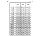
- FIG. 8 shows an example of the inspection result of the dynamic characteristic inspection when there are N probe heads 3 .
- the inspection result 63 shown in FIG. 7 and the inspection result 64 shown in FIG. 8 are examples in which specific numerical values are described.
- the inspection result 61 shown in FIG. 5 is the first inspection result for 15 days for a certain inspection item.
- the inspection result 62 shown in FIG. 6 is the m-th inspection result for 15 days for the same inspection item as the inspection result 61 .
- An inspection result 64 shown in FIG. 8 is an inspection result describing the first specific numerical values for 15 days for the same inspection items as the inspection results 61 and 62 .
- the symbol PH and numbers 1, 2, 3 are attached to the probe heads 3a, 3b, 3c, respectively.
- the test results for PH1, PH2, and PH3 on January 1st are d1a0101, d2a0101, and d3a0101, respectively.
- the number on the right side of "d” is the number of the probe head, "a” is the symbol indicating the inspection item, the two-digit number on the right side of "a” indicates the date, and the two-digit number on the right is the inspection date.
- the ordinal number of the test is indicated by m.
- the inspection results in each column of inspection results 61 and 62 are, for example, inspection value data data1 of different semiconductor devices 2 or inspection result data data3 of semiconductor devices 2, respectively. Since the inspection result data data3 includes the inspection value data data1 and the non-defective product determination result data2, the inspection results in each column of the inspection results 61 and 62 can be made into two-dimensional vectors. That is, the inspection result data data3 is represented by, for example, a two-dimensional vector. Incidentally, it is assumed that the inspection result data data3 is written in each column of the inspection results 61 and 62 as appropriate.
- inspection result data data3 of the first probe head 3a that is, PH1 from January 1 to January 15 are d1a0101 to d1a1501, respectively.
- the inspection result data data3 of the second probe head 3b that is, PH2 from January 1 to January 15 are d2a0101 to d2a1501, respectively, and from January 1 to January 15.
- 3 probe head 3c that is, inspection result data data3 of PH3 are d3a0101 to d3a1501, respectively.
- inspection result data data3 of PH1 from January 1 to January 15 are d1a01m to d1a15m, respectively.
- the inspection result data data3 of PH2 from January 1 to January 15 are d2a01m to d2a15m, respectively, and the inspection result data data3 of PH3 from January 1 to January 15 are respectively d3a01m to d3a15m.
- 5 to 7 show an example in which the inspection results are arranged in date order, they may be arranged in order of individually set device numbers or the like.
- the analysis unit 15 analyzes whether the inspection value data data1 in the inspection results of each probe head 3 is normally distributed. If the distribution is not normal, the analysis unit 15 determines that the probe head 3 that is not normally distributed is abnormal.
- the normal distribution analysis for analyzing whether or not the data are normally distributed is determined, for example, from the chi-square values of the target data using the values in the chi-square distribution table at a significance level of 5%.
- a chi-square distribution table is a table of critical values according to statistical degrees of freedom and significance levels. For example, the critical value at 1 degree of freedom and 5% significance level is 3.84.
- the analysis unit 15 outputs an abnormality determination light emission signal sig1 indicating an abnormality determination and an abnormality determination alarm signal sig2 to the warning unit 41 via the control unit 17 .
- the analysis unit 15 performs a second analysis.
- the analysis unit 15 determines that there is no difference between the probe heads 3 from the inspection results of all the probe heads 3 that are performing inspection. or detect significant differences between the probe heads 3 using analysis of variance. Determination of whether or not there is a significant difference in the analysis of variance, that is, determination of significance, is performed at a significance level of 5%.
- FIGS. 5 to 7 show examples in which the target range for significant difference determination is 15 data for each of the three probe heads 3a, 3b, and 3c. In FIG. 8, three probe heads, that is, PH1, PH2, and PH3, are shown as the target range of the significant difference determination performed first. From the second time onwards, it is set within three of PH4 to PHN, which are next to PH3.
- the analysis unit 15 performs a third analysis.
- the analysis unit 15 identifies which probe head 3 has a significant difference compared to other probe heads 3 by multiple comparison.
- the probe heads 3 to be compared are divided. For example, when the number of probe heads 3 is 6, the comparison among the first to third probe heads 3, PH1 to PH3, and the fourth to sixth probe heads 3, PH4 -Compare in PH6.
- the maximum number of subjects for multiple comparisons should be 4 or less.
- the Bonferroni method As a method of multiple comparison, first, it is determined whether there is a significant difference between the probe heads 3 as follows. Multiple comparisons use, for example, the Bonferroni method. For example, consider a case where three probe heads 3 are used for inspection as shown in FIG. In the comparison with three probe heads 3, 5%/3 is the significance level, and between each set of two probe heads 3, namely the first probe head 3a, PH1 and the second probe head 3b, PH2 , between PH1 and the third probe head 3c or PH2, and between PH2 and PH3.
- the analysis unit 15 outputs, via the control unit 17, an abnormality determination light emission signal sig1 and an abnormality determination alarm signal sig2 indicating an abnormality determination of PH2 to the warning unit 41.
- a light emitter 32 provided on the second probe head 3b emits light.
- the method of multiple comparison is not limited to the Bonferroni method. It can be arbitrarily set depending on the data to be analyzed.
- FIGS. 2 to 4 show an example in which the light emitter 32 of the warning unit 41 is provided in each probe head 3 and it is possible to determine which probe head 3 has an abnormality.
- Information on the probe head 3 in which an abnormality has occurred that is, information on the abnormality of the probe head 3 may be displayed on the operation unit 5 .
- the operation unit 5 displays the number of the probe head 3 set so that it can be known which probe head 3 has an abnormality.
- the abnormality information of the probe head 3 displayed on the operation unit 5 does not have to be the probe number.
- the color of the picture may be changed.
- the analysis conditions are, for example, the number of data, the period, the judgment value, and the method for the significant difference judgment by the analysis unit 15 .
- the setting of the number of data includes, for example, setting using the past 100 test results from the latest test result, setting using the past 50 test results, and the like.
- the setting of the period includes, for example, setting using test results for the past 10 days from the latest test result, setting using test results for the past 5 days, and the like.
- the setting of the judgment value is the setting of a reference value for judging whether there is a significant difference, for example, the setting of 5%, the setting of 1%, and the like.
- the setting of the method is the setting of the determination method, and sets whether to use the inspection result data data3 or to use the processed value of the inspection result data data3. For example, there is a setting for judging a significant difference based on the percentage of non-defective products or a ratio of defective products for all inspection items, and a setting for judging a significant difference based on the average value of one inspection item.
- the non-defective product rate or the defective product rate is a ratio based on the non-defective product determination result data2.
- the average value of one inspection item described above is a processed value of the inspection value data data1, and is, for example, an average value of voltage or the like.
- a device inspection method of the device inspection apparatus 50 tests a plurality of semiconductor devices 2 in parallel.
- the device inspection apparatus 50 inspects the semiconductor device 2 (inspection determination procedure).
- a probe head 3 having a probe 33 that contacts the electrode 11 of the semiconductor device 2 is used for each semiconductor device 2 to measure test value data data1 for each semiconductor device 2 .
- the inspection determination unit 18 determines the inspection value data data1 (inspection determination procedure). The inspection determination unit 18 determines whether the semiconductor device 2 is good or defective based on the inspection value data data1.
- the inspection value data data1 and the determination result of step ST02 are stored in the storage unit 16 (storage procedure).
- the storage unit 16 stores the inspection result data data3 including the inspection value data data1 and the judgment result (defective product judgment result data2) of the semiconductor device 2 in step ST02.
- step ST04 analysis is performed by statistical processing in the analysis unit 15 (analysis procedure).
- analysis unit 15 statistical processing is performed based on a plurality of inspection result data data3 existing for each inspection item stored in the storage procedure of step ST03, and a significant difference is found between the plurality of inspection result data data3 for each probe head 3. Whether or not there is a difference is analyzed, and if there is a significant difference, it is determined that the probe head 3 is abnormal.
- a warning is issued using the warning unit 41 in the case of an abnormality determination (warning procedure).
- Device inspection apparatus 50 indicates the result of abnormality determination to warning unit 41 .
- step ST06 it is determined whether or not the semiconductor device 2 to be inspected remains. If there are still objects to be inspected, the process returns to step ST01, and steps ST01 to ST05 are executed. If there are no objects to be inspected, the process ends.
- the functions of the control unit 17, the inspection determination unit 18, and the analysis unit 15 are realized by a processor 98 and a memory 99 provided in the computer 8.
- the control unit 17 , the inspection determination unit 18 , and the analysis unit 15 are implemented by the processor 98 executing programs stored in the memory 99 . Also, multiple processors 98 and multiple memories 99 may cooperate to perform each function.
- the storage unit 16 is an area of the memory 99 that is used by the computer 8 for calculations, which is different from the storage area for programs.
- the control unit 17, the inspection determination unit 18, and the analysis unit 15 are configured by application software.
- the functions of the control unit 17, the inspection determination unit 18, and the analysis unit 15 may be implemented by the processor 98 and the memory 99, and may be configured by devices other than the computer 8.
- Probe abnormalities that misjudge non-defective products as defective also occur in the following cases.
- the semiconductor device 2 is placed in a predetermined location of the device inspection apparatus 50, that is, the concave portion 26 of the housing 1, and the probe head 3 is moved by the moving mechanism 20 such as the air cylinder 23 and the actuator 24. Moved, the probes 33 of the probe head 3 come into contact with the electrodes 11 of the semiconductor device 2 .
- the moving mechanism 20 malfunctions, the probe head 3 collides with the semiconductor device 2 to be inspected, which damages the probe head 3 and causes an abnormality in the probe head 3 such as bending of the probe 33.
- abnormalities in the probe head 3 may be caused by deformation of the tip of the probe 33, adhesion of foreign matter, breakage of the spring in the probe in the case of contact probes, and the like.
- the contact failure between the semiconductor device 2 to be inspected and the probe head 3 does not occur in every measurement, and the contact failure may or may not occur. Therefore, it is difficult to determine whether the semiconductor device 2 is faulty or the probe head 3 is faulty unless some contrivance is made. Furthermore, in an apparatus that inspects a plurality of semiconductor devices 2 in parallel using a plurality of probe heads 3, it is possible to determine which probe head 3 caused the collision between the probe head 3 and the semiconductor device 2 unless some kind of contrivance is made. In some cases, it is difficult to identify the probe head 3 in which an abnormality has occurred.
- the device inspection apparatus 50 of Embodiment 1 analyzes whether there is a significant difference between the plurality of inspection result data data3 for each probe head 3 by statistical processing based on the plurality of inspection result data data3 stored in the storage unit 16. Therefore, at the end of the device inspection of the semiconductor device 2 to be inspected, an abnormality of the probe head 3 can be detected together with the result of the inspection object, that is, the non-defective product determination result data2.
- Abnormalities in the probe head 3 include failures of the probe head 3 and signs of failure. Signs of failure include occasional inspection failures and frequent occurrence of inspection results that differ from normal values.
- One of the causes of a sign of failure is that a foreign object or the like gets caught in the probe 33 of the probe head 3 . This is similar to the attachment of foreign matter to the tip of the probe 33 described above.
- inspection is performed using a monitor sample or the like in order to distinguish whether the failure is caused by the probe head or by the test object. Through this inspection, the cause is isolated, and if the problem is caused by the probe head, the probe head is replaced or repaired. If the probe head 3 has completely failed rather than being a sign of failure, it is conceivable that many defects will occur only in the failed probe head 3 .
- the device inspection apparatus 50 of the first embodiment inspects the semiconductor device 2 to be inspected to the end without stopping the inspection halfway even if an abnormality in the probe head 3 is detected.
- a semiconductor device 2 that has been determined to be defective due to an abnormality in the probe head 3 is subjected to maintenance such as replacement, repair, and foreign matter removal of the probe head 3, and then inspected again.
- the device inspection apparatus 50 and the device inspection method of the first embodiment can perform dynamic characteristic inspection on a plurality of semiconductor devices 2 in parallel, i.e., at the same time, using a plurality of probe heads 3. It is possible to analyze whether an abnormality has occurred. Furthermore, in the device inspection apparatus 50 and the device inspection method of the first embodiment, when an abnormality of the probe head 3 is detected, the operator can be notified by ringing or emitting light from the operation unit 5 and the warning unit 41. . Even when the status of automatic operation is displayed on the operation unit 5, the probe head 3 in which an abnormality has occurred can be visually recognized by causing the light emitter 32 of the warning unit 41 to emit light. The device inspection apparatus 50 and the device inspection method of the first embodiment can arbitrarily set the conditions for analysis, that is, the number of data, the period, the judgment value, and the method. can be adjusted.
- the device inspection apparatus 50 and the device inspection method of Embodiment 1 can detect an abnormality of the probe head 3, including a failure and malfunction of the probe head 3, during inspection. be able to.
- the device inspection apparatus 50 and the device inspection method of the first embodiment can detect an abnormality of the probe head 3 during inspection, so that it is possible to avoid erroneously determining that the semiconductor device 2, which is originally a non-defective product, is defective. can be prevented from being discarded.
- the device inspection apparatus 50 and the device inspection method of the first embodiment can correctly measure the inspection value data data1, so that the correct yield, inspection distribution, and the like can be obtained.
- the device inspection apparatus 50 of Embodiment 1 is a device inspection apparatus that inspects a plurality of semiconductor devices 2 in parallel.
- a plurality of probe heads 3 having probes 33 in contact with electrodes 11 and individually used for each semiconductor device 2, and applying an electric signal for each semiconductor device 2 to a plurality of semiconductor devices 2 to obtain an inspection value for each semiconductor device 2.
- It includes an inspection unit 4 that measures data data1, and an inspection determination unit 18 that determines whether the semiconductor device 2 is good or defective based on the inspection value data data1.
- the device inspection apparatus 50 further includes a storage unit 16 for storing inspection result data data3 including inspection value data data1 and the result of judgment of the semiconductor device 2 (non-defective product judgment result data2); By statistical processing based on a plurality of inspection result data data3 existing for each inspection item, whether there is a significant difference between the plurality of inspection result data data3 for each probe head 3 is analyzed, and if there is a significant difference, the relevant An analysis unit 15 that determines that the probe head 3 is abnormal, and a warning unit 41 that indicates the result of the abnormality determination in the analysis unit 15 that the probe head 3 is abnormal.
- the device inspection apparatus 50 detects a significant difference between the plurality of inspection result data data3 for each probe head 3 by statistical processing based on the plurality of inspection result data data3 recorded in the storage unit 16. Since it is analyzed whether or not there is any, an abnormality of the probe head 3 can be detected together with the result of the inspection target (semiconductor device 2) at the end of the device inspection of the inspection target (semiconductor device 2).
- the device inspection method of the first embodiment is a device inspection method for inspecting a plurality of semiconductor devices 2 in parallel, and includes a plurality of probe heads 3 having a plurality of probes 33 contacting a plurality of electrodes 11 for each semiconductor device 2. and an inspection determination procedure for determining whether the semiconductor device 2 is good or defective based on the inspection value data data1. .
- the device inspection method further includes a storage procedure for storing inspection result data data3 including inspection value data data1 and a judgment result (non-defective product judgment result data2) of the semiconductor device 2; Perform statistical processing based on a plurality of inspection result data data3 existing for each inspection item, analyze whether there is a significant difference between the plurality of inspection result data data3 for each probe head 3, and if there is a significant difference, the probe It includes an analysis procedure for determining that the head 3 is abnormal, and a warning procedure indicating the result of abnormality determination that the probe head 3 is abnormal in the analysis procedure.
- the device inspection method of the first embodiment performs statistical processing based on the plurality of inspection result data data3 recorded in the storage procedure, and finds a significant difference between the plurality of inspection result data data3 for each probe head 3. Since it is analyzed whether or not there is an abnormality, an abnormality of the probe head 3 can be detected together with the result of the inspection target (semiconductor device 2) when the device inspection of the inspection target (semiconductor device 2) is completed.
- FIG. 11 is a diagram showing the configuration of a device inspection apparatus according to the second embodiment
- FIG. 12 is a diagram showing an example of inspection results according to the second embodiment.
- the device inspection apparatus 50 of the second embodiment is different from the device inspection apparatus 50 of the first embodiment in that one semiconductor device 2 is inspected in one inspection.
- the parts different from the device inspection apparatus 50 of the first embodiment will be mainly described.
- FIG. 11 shows an example in which one semiconductor device 2 is mounted on the housing 1 and the probes 33 of one probe head 3 are in contact with the electrodes 11 of the semiconductor device 2 .
- the operation unit 5 and the alarm 6 are omitted in FIG. Only three of the plurality of electrodes 11 in semiconductor device 2 are shown.
- the past inspection result of the single probe head and the latest inspection result are compared to analyze whether there is a significant difference in the latest inspection result. By analyzing in this way, it is detected whether there is an abnormality in the probe head 3 being inspected.
- the probe head In 3 the latest inspection result and the past inspection result are used.
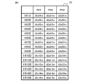
- the inspection results 65 shown in FIG. 12 are the first to m-th inspection results for 15 days for a certain inspection item in the first probe head 3 .
- the inspection results for January 1 are d1a0101 to d1a01m.
- the number on the right side of "d" is the number of the probe head
- "a" is the symbol indicating the inspection item
- the two-digit number on the right side of "a” indicates the date.
- the two digits to the right of indicates the ordinal number of the test. Note that the ordinal number of the m-th inspection is indicated by m.
- the first inspection result data data3 from January 1st to January 15th are d1a0101 to d1a1501, respectively.
- the second inspection result data data3 from January 1 to January 15 are d1a0102 to d1a1502, respectively
- the third inspection result data data3 from January 1 to January 15 are respectively d1a0103. to d1a1503
- m-th inspection result data data3 from January 1 to January 15 are d1a01m to d1a15m, respectively.
- the conditions for performing analysis by the analysis unit 15 are arbitrarily set as part of the operation of the computer 8 from the operation unit 5. be.
- the analysis conditions are, for example, the number of data, the period, the judgment value, and the method for the significant difference judgment by the analysis unit 15 .
- a recess 26 for mounting the semiconductor device 2 is formed on the device mounting surface 25 of the housing 1 . Note that the concave portion 26 is omitted in FIG. 11 .
- the inspection unit 4 applies an electric signal to the semiconductor device 2 and measures inspection value data data1 of the semiconductor device 2 .
- the inspection determination unit 18 determines whether the semiconductor device 2 is a non-defective product or a defective product based on the inspection value data data1.
- the storage unit 16 stores inspection result data data3 including inspection value data data1 and the result of non-defective product determination of the semiconductor device 2, that is, non-defective product determination result data2.
- the analysis unit 15 analyzes whether there is a significant difference between the plurality of test result data data3 by statistical processing based on the plurality of test result data data3 existing for each test item stored in the storage unit 16, and determines whether there is a significant difference. If there is, it is determined that the probe head 3 is abnormal. Determining that the probe head is abnormal is determining that the probe head is abnormal.
- the warning unit 41 indicates the result of the abnormality determination of the probe head 3 by light and/or sound.
- a device inspection method of the device inspection apparatus 50 of the second embodiment inspects one semiconductor device 2 .
- the device inspection apparatus 50 inspects the semiconductor device 2 (inspection determination procedure).
- the test value data data1 of the semiconductor device 2 is measured using the probe head 3 having the probes 33 that contact the electrodes 11 of the semiconductor device 2 .
- the inspection determination unit 18 determines the inspection value data data1 (inspection determination procedure).
- the inspection determination unit 18 determines whether the semiconductor device 2 is good or defective based on the inspection value data data1.
- the inspection value data data1 and the determination result of step ST02 are stored in the storage unit 16 (storage procedure).
- the storage unit 16 stores the inspection result data data3 including the inspection value data data1 and the judgment result (defective product judgment result data2) of the semiconductor device 2 in step ST02.
- step ST04 analysis is performed by statistical processing in the analysis unit 15 (analysis procedure).
- the analysis unit 15 performs statistical processing based on the plurality of inspection result data data3 existing for each inspection item stored in the storage procedure of step ST03, and determines whether there is a significant difference between the plurality of inspection result data data3. If there is a significant difference, it is determined that the probe head 3 is abnormal.
- step ST05 a warning is issued using the warning unit 41 in the case of an abnormality determination (warning procedure).
- Device inspection apparatus 50 indicates the result of abnormality determination to warning unit 41 .
- step ST06 it is determined whether or not the semiconductor device 2 to be inspected remains. If there are still objects to be inspected, the process returns to step ST01, and steps ST01 to ST05 are executed. If there are no objects to be inspected, the process ends.
- the target data for detecting an abnormality in the probe head 3 are the most recent inspection result and the past inspection result of the same probe head 3. Abnormalities in the probe head 3 can be detected even when the devices 2 are not tested in parallel.
- the device inspection apparatus 50 of the second embodiment is a device inspection apparatus for inspecting the semiconductor device 2, and includes the housing 1 on which the semiconductor device 2 is mounted and the probes that contact the electrodes 11 of the semiconductor device 2. 33, an inspection unit 4 that applies an electric signal to the semiconductor device 2 to measure inspection value data data1 of the semiconductor device 2, and a non-defective product or a defective semiconductor device 2 based on the inspection value data data1. and an inspection determination unit 18 for determining whether.
- the device inspection apparatus 50 according to the second embodiment further includes a storage unit 16 for storing inspection result data data3 including inspection value data data1 and the result of judgment of the semiconductor device 2 (non-defective product judgment result data2).
- Statistical processing based on a plurality of inspection result data data3 existing for each inspection item is analyzed to determine whether there is a significant difference between the plurality of inspection result data data3, and if there is a significant difference, the probe head 3 is abnormal.
- the device inspection apparatus 50 of Embodiment 2 analyzes whether there is a significant difference between the plurality of inspection result data data3 by statistical processing based on the plurality of inspection result data data3 recorded in the storage unit 16. Therefore, at the end of the device inspection of the inspection object (semiconductor device 2), the abnormality of the probe head 3 can be detected together with the result of the inspection object (semiconductor device 2).
- a device inspection method is a device inspection method for inspecting a semiconductor device 2, and uses a probe head 3 having probes 33 that come into contact with electrodes 11 of the semiconductor device 2 to obtain inspection value data of the semiconductor device 2. It includes an inspection procedure for measuring data1 and an inspection determination procedure for determining whether the semiconductor device 2 is good or bad based on the inspection value data data1.
- the device inspection method according to the second embodiment further comprises a storage procedure for storing inspection result data data3 including inspection value data data1 and a judgment result (non-defective product judgment result data2) of the semiconductor device 2; Statistical processing is performed based on a plurality of inspection result data data3 existing for each inspection item, and whether or not there is a significant difference between the plurality of inspection result data data3 is analyzed.
- the device inspection method of the second embodiment performs statistical processing based on the plurality of inspection result data data3 recorded in the storage procedure, and analyzes whether there is a significant difference between the plurality of inspection result data data3. Therefore, at the end of the device inspection of the inspection object (semiconductor device 2), the abnormality of the probe head 3 can be detected together with the result of the inspection object (semiconductor device 2).
- FIG. 13 is a diagram showing the configuration of a device inspection apparatus according to the third embodiment.
- a device inspection apparatus 50 according to the third embodiment differs from the device inspection apparatus 50 according to the first embodiment in that the light emitter 32 of the warning section 41 is provided at a different location from the main body 34 of the probe head 3 .
- the parts different from the device inspection apparatus 50 of the first embodiment will be mainly described.
- the light emitters 32 are not arranged on the main body 34 of each probe head 3, and instead the light emitters 32 corresponding to the probe heads 3 are collectively arranged in the light emitter section 9 of the housing 1. I gave an example. Note that the operation unit 5 and the alarm 6 are omitted in FIG.
- the light-emitting unit 9 shown in FIG. 13 is an example of being arranged on the front side in the x direction of the housing 1, and the location on the front side in the x direction is an example of a location that is easily visible to the operator. If there are N probe heads 3 , the light emitter section 9 has N light emitters 32 .
- the light-emitting unit 9 is not limited to the front side of the housing 1 in the x-direction, and may be installed at a place where the device inspection apparatus 50 can easily be visually recognized.
- the probe head 3 may be located in a location that is difficult for the operator to visually recognize. Even in this case, the device inspection apparatus 50 of Embodiment 3 can easily confirm the abnormality of each probe head 3 .
- the light emitter 32 of the warning section 41 may be located in the light emitter section 9 together with the main body 34 of each probe head 3 . If the light emitters 32 are provided at a plurality of locations, the malfunction of each probe head 3 can be quickly confirmed by the one that is easy to confirm.
- the device inspection apparatus 50 of the second embodiment has shown an example in which the light emitter 32 of the warning unit 41 is arranged in the main body 34 of the probe head 3, the device inspection apparatus 50 of the third embodiment , the light-emitting device 32 may be arranged in a place such as the housing 1 that is easily visible to the operator.
Landscapes
- Engineering & Computer Science (AREA)
- Manufacturing & Machinery (AREA)
- Computer Hardware Design (AREA)
- Microelectronics & Electronic Packaging (AREA)
- Power Engineering (AREA)
- Testing Of Individual Semiconductor Devices (AREA)
Abstract
Un appareil d'inspection de dispositifs (50) comprend : une pluralité de têtes de sonde (3) ; une unité d'inspection (4) qui mesure des données de valeurs d'inspection (données 1) pour chaque dispositif à semi-conducteur (2) ; une unité de stockage (16) qui stocke des données de résultat d'inspection (données 3) comprenant les données de valeurs d'inspection (données 1) et un résultat (données 2) de détermination pour le dispositif à semi-conducteur (2) ; et une unité d'analyse (15) qui, au moyen d'un traitement statistique basé sur une pluralité d'éléments de données de résultat d'inspection (données 3) qui sont présents pour chaque élément d'inspection enregistré dans l'unité de stockage (16), effectue une analyse pour déterminer s'il existe une différence significative entre une pluralité d'élements de données de résultat d'inspection (données 3) pour chaque tête de sonde (3) et détermine que la tête de sonde (3) est anormale si la différence est considérable.
Priority Applications (2)
| Application Number | Priority Date | Filing Date | Title |
|---|---|---|---|
| PCT/JP2022/006941 WO2023157291A1 (fr) | 2022-02-21 | 2022-02-21 | Appareil et procédé d'inspection de dispositifs |
| JP2022542725A JP7241978B1 (ja) | 2022-02-21 | 2022-02-21 | デバイス検査装置及びデバイス検査方法 |
Applications Claiming Priority (1)
| Application Number | Priority Date | Filing Date | Title |
|---|---|---|---|
| PCT/JP2022/006941 WO2023157291A1 (fr) | 2022-02-21 | 2022-02-21 | Appareil et procédé d'inspection de dispositifs |
Publications (1)
| Publication Number | Publication Date |
|---|---|
| WO2023157291A1 true WO2023157291A1 (fr) | 2023-08-24 |
Family
ID=85600328
Family Applications (1)
| Application Number | Title | Priority Date | Filing Date |
|---|---|---|---|
| PCT/JP2022/006941 WO2023157291A1 (fr) | 2022-02-21 | 2022-02-21 | Appareil et procédé d'inspection de dispositifs |
Country Status (2)
| Country | Link |
|---|---|
| JP (1) | JP7241978B1 (fr) |
| WO (1) | WO2023157291A1 (fr) |
Citations (3)
| Publication number | Priority date | Publication date | Assignee | Title |
|---|---|---|---|---|
| JPH04249335A (ja) * | 1991-02-05 | 1992-09-04 | Matsushita Electron Corp | プローブ検査システム |
| WO2020075327A1 (fr) * | 2018-10-12 | 2020-04-16 | 株式会社アドバンテスト | Dispositif d'analyse, procédé d'analyse et programme d'analyse |
| JP2021025971A (ja) * | 2019-08-08 | 2021-02-22 | 株式会社日本ロック | 通電検査装置及び通電検査方法 |
-
2022
- 2022-02-21 JP JP2022542725A patent/JP7241978B1/ja active Active
- 2022-02-21 WO PCT/JP2022/006941 patent/WO2023157291A1/fr active Application Filing
Patent Citations (3)
| Publication number | Priority date | Publication date | Assignee | Title |
|---|---|---|---|---|
| JPH04249335A (ja) * | 1991-02-05 | 1992-09-04 | Matsushita Electron Corp | プローブ検査システム |
| WO2020075327A1 (fr) * | 2018-10-12 | 2020-04-16 | 株式会社アドバンテスト | Dispositif d'analyse, procédé d'analyse et programme d'analyse |
| JP2021025971A (ja) * | 2019-08-08 | 2021-02-22 | 株式会社日本ロック | 通電検査装置及び通電検査方法 |
Also Published As
| Publication number | Publication date |
|---|---|
| JPWO2023157291A1 (fr) | 2023-08-24 |
| JP7241978B1 (ja) | 2023-03-17 |
Similar Documents
| Publication | Publication Date | Title |
|---|---|---|
| KR102239051B1 (ko) | 검사 시스템, 및 검사 시스템의 고장 해석 및 예지 방법 | |
| US6903360B2 (en) | Method for detecting missing components at electrical board test using optoelectronic fixture-mounted sensors | |
| US20070164763A1 (en) | Method for detecting abnormality of probe card | |
| JP2010525365A (ja) | 試験ソケット内で破損ピンを検出するための方法および装置 | |
| JP2013238554A (ja) | 検査装置 | |
| US20170205442A1 (en) | Semiconductor device inspection apparatus and semiconductor device inspection method | |
| JP7241978B1 (ja) | デバイス検査装置及びデバイス検査方法 | |
| CN106960804B (zh) | 评价装置、探针位置的检查方法 | |
| JP2007103860A (ja) | プローブ接触痕検出方法、及び、プローバ | |
| CN115938255A (zh) | 显示检测装置、检测方法及检测系统 | |
| KR100304045B1 (ko) | 전도성 도선상의 미세 단락에 의한 접촉불량 감지 방법 | |
| KR102250982B1 (ko) | 디스플레이 패널의 전기 검사장치 및 방법 | |
| TWI460431B (zh) | 設有彈簧針(pogo pin)之探針單元及利用其之基板修復裝置 | |
| JP2752940B2 (ja) | キーボード試験装置 | |
| JP2011215007A (ja) | 試験装置及び試験方法 | |
| CN112798109A (zh) | 一种主板质量的检测评价装置 | |
| KR100984716B1 (ko) | 엘이디 칩 측정결과의 보정방법 및 이를 위한 보정장치 | |
| TWI629473B (zh) | 組裝電路板檢測系統及組裝電路板檢測方法 | |
| US20230384365A1 (en) | Wafer test system and operating method thereof | |
| JP6046426B2 (ja) | 基板検査装置および基板検査方法 | |
| JP2013140117A (ja) | 半導体装置の製造方法及び半導体試験装置 | |
| JP6058325B2 (ja) | 基板検査装置および基板検査方法 | |
| US20240142213A1 (en) | Temperature Correction for Dimensional Measurement | |
| TWI745197B (zh) | 定位機構、作業機、測試機及測試設備 | |
| CN117288987A (zh) | 用于芯片测试的插座组件以及芯片测试系统 |
Legal Events
| Date | Code | Title | Description |
|---|---|---|---|
| WWE | Wipo information: entry into national phase |
Ref document number: 2022542725 Country of ref document: JP |
|
| 121 | Ep: the epo has been informed by wipo that ep was designated in this application |
Ref document number: 22927191 Country of ref document: EP Kind code of ref document: A1 |