WO2023157291A1 - Device inspection apparatus and device inspection method - Google Patents
Device inspection apparatus and device inspection method Download PDFInfo
- Publication number
- WO2023157291A1 WO2023157291A1 PCT/JP2022/006941 JP2022006941W WO2023157291A1 WO 2023157291 A1 WO2023157291 A1 WO 2023157291A1 JP 2022006941 W JP2022006941 W JP 2022006941W WO 2023157291 A1 WO2023157291 A1 WO 2023157291A1
- Authority
- WO
- WIPO (PCT)
- Prior art keywords
- inspection
- semiconductor device
- probe head
- unit
- result
- Prior art date
Links
- 238000007689 inspection Methods 0.000 title claims abstract description 409
- 238000000034 method Methods 0.000 title claims description 83
- 239000000523 sample Substances 0.000 claims abstract description 231
- 239000004065 semiconductor Substances 0.000 claims abstract description 163
- 238000004458 analytical method Methods 0.000 claims abstract description 76
- 230000002159 abnormal effect Effects 0.000 claims abstract description 34
- 238000012545 processing Methods 0.000 claims abstract description 26
- 230000005856 abnormality Effects 0.000 claims description 71
- 230000002950 deficient Effects 0.000 claims description 63
- 238000012360 testing method Methods 0.000 claims description 30
- 238000010586 diagram Methods 0.000 description 21
- 230000007246 mechanism Effects 0.000 description 14
- 230000006870 function Effects 0.000 description 7
- 230000015654 memory Effects 0.000 description 5
- 230000008569 process Effects 0.000 description 5
- 239000000758 substrate Substances 0.000 description 4
- 238000000540 analysis of variance Methods 0.000 description 3
- 230000007257 malfunction Effects 0.000 description 3
- 239000004593 Epoxy Substances 0.000 description 2
- 238000005516 engineering process Methods 0.000 description 2
- 239000011521 glass Substances 0.000 description 2
- 239000013598 vector Substances 0.000 description 2
- 238000005452 bending Methods 0.000 description 1
- 238000004364 calculation method Methods 0.000 description 1
- 239000003990 capacitor Substances 0.000 description 1
- 230000008859 change Effects 0.000 description 1
- 238000004140 cleaning Methods 0.000 description 1
- 230000007547 defect Effects 0.000 description 1
- 238000001514 detection method Methods 0.000 description 1
- 238000000605 extraction Methods 0.000 description 1
- 238000012423 maintenance Methods 0.000 description 1
- 238000005259 measurement Methods 0.000 description 1
- 230000004048 modification Effects 0.000 description 1
- 238000012986 modification Methods 0.000 description 1
- 230000008439 repair process Effects 0.000 description 1
- 230000000717 retained effect Effects 0.000 description 1
- 230000003068 static effect Effects 0.000 description 1
- 238000010998 test method Methods 0.000 description 1
Images


Classifications
-
- H—ELECTRICITY
- H01—ELECTRIC ELEMENTS
- H01L—SEMICONDUCTOR DEVICES NOT COVERED BY CLASS H10
- H01L22/00—Testing or measuring during manufacture or treatment; Reliability measurements, i.e. testing of parts without further processing to modify the parts as such; Structural arrangements therefor
Definitions
- This application relates to a device inspection apparatus and a device inspection method.
- Japanese Unexamined Patent Application Publication No. 2002-100001 discloses a prober device and a semiconductor device inspection method for inspecting a plurality of chips formed on a semiconductor wafer in parallel in a wafer state. As the number of chips to be inspected increases, the contact resistance between the probe block and the electrodes of the chip increases, resulting in erroneous determination of defective products.
- the semiconductor device inspection method using the prober device of Patent Document 1 as the number of chips to be inspected increases, chips that have been erroneously determined to be defective are reinspected, so that chips to be reinspected are selected. a step of cleaning a plurality of probe blocks; and a step of selecting one probe block to be used for retesting from the plurality of probe blocks used in parallel testing of a plurality of chips.
- the device inspection which inspects the electrical characteristics, etc. of the semiconductor device to be inspected, is not limited to the wafer state, but may be performed in the separated chip state.
- Device inspection for inspecting an object to be inspected includes a method of inspecting by bringing electrodes of the object to be inspected into contact with a plurality of probes attached to a probe head.
- the probe head has a plurality of probes and corresponds to the probe block of Patent Document 1.
- an abnormality occurs in the probe that causes contact failure between the inspection object and the probe.
- a non-defective product is erroneously determined as a defective product.
- the non-defective product rate for each probe block is calculated based on the inspection results read after all the chips on the wafer have been inspected. Abnormalities in the probe block (probe head) cannot be detected in the first inspection.
- the technology disclosed in the specification of the present application aims to detect an abnormality of the probe head together with the result of the inspection target when the inspection of the device to be inspected ends.
- An example device inspection apparatus disclosed in the specification of the present application includes a housing for mounting a plurality of semiconductor devices, a plurality of probe heads that have probes that contact electrodes of the semiconductor devices, and is used individually for each semiconductor device, An inspection unit that applies an electrical signal for each semiconductor device to a plurality of semiconductor devices and measures inspection value data for each semiconductor device, and an inspection judgment that determines whether the semiconductor device is a non-defective product or a defective product based on the inspection value data. and An example of the device inspection apparatus disclosed in the present specification further includes a storage unit for storing inspection result data including inspection value data and semiconductor device judgment results, and each inspection item stored in the storage unit.
- Analysis unit that analyzes whether there is a significant difference between multiple inspection result data for each probe head by statistical processing based on multiple inspection result data, and determines that the probe head is abnormal when there is a significant difference and a warning unit that indicates the result of abnormality determination that the probe head is abnormal in the analysis unit.
- An example device inspection apparatus disclosed in the present specification analyzes whether there is a significant difference between a plurality of inspection result data for each probe head by statistical processing based on a plurality of inspection result data stored in a storage unit. Therefore, it is possible to detect an abnormality of the probe head together with the result of the inspection target at the end of the inspection of the device to be inspected.
- FIG. 1 is a diagram showing the configuration of a device inspection apparatus according to Embodiment 1;
- FIG. 2 is a diagram showing an inspection target and a probe head mounted on the housing of FIG. 1;
- FIG. 3 is a diagram showing the probe head of FIG. 2 and an object to be inspected;
- FIG. 3 is a diagram showing a moving mechanism of the probe head of FIG. 2;
- FIG. FIG. 5 is a diagram showing an example of inspection results according to Embodiment 1;
- FIG. FIG. 5 is a diagram showing an example of inspection results according to Embodiment 1;
- FIG. FIG. 5 is a diagram showing an example of inspection results according to Embodiment 1;
- FIG. FIG. 5 is a diagram showing an example of inspection results according to Embodiment 1;
- FIG. FIG. 5 is a diagram showing an example of inspection results according to Embodiment 1;
- FIG. 5 is a diagram showing an example of inspection results according to Embodiment 1;
- FIG. 5 is
- FIG. 4 is a flowchart showing a device inspection method according to Embodiment 1; 2 is a diagram showing a hardware configuration example that implements the functions of a control unit, an inspection determination unit, and an analysis unit in FIG. 1; FIG. FIG. 10 is a diagram showing the configuration of a device inspection apparatus according to Embodiment 2; FIG. 10 is a diagram showing an example of inspection results according to Embodiment 2; FIG. 10 is a diagram showing the configuration of a device inspection apparatus according to Embodiment 3;
- FIG. 1 is a diagram showing the configuration of a device inspection apparatus according to Embodiment 1.
- FIG. FIG. 2 is a diagram showing the test object and the probe head mounted on the housing of FIG. 1
- FIG. 3 is a diagram showing the probe head and the test object of FIG. 4 is a diagram showing a moving mechanism of the probe head of FIG. 2.
- FIG. 5 to 8 are diagrams showing examples of inspection results according to the first embodiment, respectively.
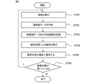
- FIG. 9 is a flow chart showing the device inspection method according to the first embodiment
- FIG. 10 is a diagram showing a hardware configuration example realizing the functions of the control unit, inspection determination unit, and analysis unit shown in FIG.
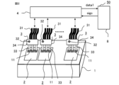
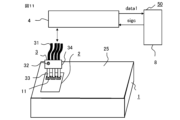
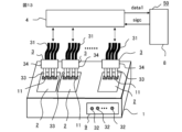
- a device inspection apparatus 50 of Embodiment 1 has a housing 1 for mounting a semiconductor device 2 to be inspected, a plurality of probes 33 , and at least one probe head 3 and an electrical signal to the semiconductor device 2 .
- An inspection unit 4 that measures inspection value data data1 of the semiconductor device 2 by applying voltage, a computer 8 that controls the inspection unit 4 and performs non-defective determination of the semiconductor device 2 and abnormality determination of the probe head 3, and abnormality determination of the probe head 3.
- a warning unit 41 for indicating a result, a moving mechanism 20 for moving the probe head 3, and an operation unit 5 for operating the computer 8 and the moving mechanism 20 are provided.
- the operation unit 5 is, for example, a touch panel display.
- FIG. 2 shows an example of a device inspection apparatus 50 that inspects a plurality of semiconductor devices 2 in parallel.
- FIG. 4 shows the moving mechanism 20 in the device inspection apparatus 50 when inspecting three semiconductor devices 2 in parallel.
- the moving mechanism 20 includes an actuator 24 that moves the head fixing plate 21 to which the plurality of probe heads 3a, 3b, and 3c are fixed in the x direction parallel to the device mounting surface 25 of the housing 1, and the head fixing plate 21. It has an air cylinder 23 that moves in the y direction, which is the direction perpendicular to the device mounting surface 25 of the housing 1 .
- the y-direction is perpendicular to the x-direction.
- the moving mechanism 20 has an air cylinder fixing plate 22 to which an air cylinder 23 is fixed.
- the air cylinder 23 holds the head fixing plate 21 to which the plurality of probe heads 3a, 3b, and 3c are fixed and moves the head fixing plate 21 in the y direction.
- the air cylinder fixed plate 22 is moved in the x direction by an actuator 24 .
- the moving mechanism 20 in the device inspection apparatus 50 for inspecting N semiconductor devices 2 in parallel is also the same as the moving mechanism 20 shown in FIG. N probe heads 3 are fixed to the head fixing plate 21 .
- the semiconductor device 2 to be inspected is, for example, an infrared sensor.
- An infrared sensor is a module in which a plurality of components are mounted on a substrate such as a glass epoxy substrate.
- the infrared sensor includes an infrared sensor chip having a temperature sensor formed by a photodiode, a control circuit or control IC (Integrated Circuit) for controlling the infrared sensor chip, and electronic components such as a capacitor.
- 2 to 4 show only three of the plurality of electrodes 11 in the semiconductor device 2.
- the electrode 11 is, for example, an anode or cathode of a photodiode, an input/output electrode of a control circuit, or the like.
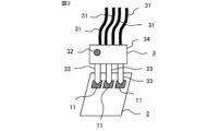
- the electrodes 11 of the semiconductor device 2 are formed on a substrate such as a glass epoxy substrate.
- the probe heads 3 and the semiconductor devices 2 to be inspected are in one-to-one correspondence, and the number of probe heads 3 and the number of semiconductor devices 2 to be inspected are the same.
- the probe head 3 includes a main body 34, a plurality of probes 33 fixed to the main body 34, and cables 31 connected to the plurality of probes 33, respectively. 2 to 4, since the light emitter 32 is provided on the main body 34 of the probe head 3, there is also a cable 31 for transmitting a signal for causing the light emitter 32 to emit light. Note that the number of cables 31 is not limited to the illustrated number.
- FIG. 4 shows a case in which there are three probe heads 3 and three semiconductor devices 2, and the three probe heads 3 are denoted by 3a, 3b, and 3c to distinguish them.
- reference numerals 2a, 2b, and 2c are attached to distinguish the three semiconductor devices 2, and reference numerals 32a, 32b, and 32c are attached to distinguish the three light emitters 32. . That is, the reference numerals for the probe heads are 3 in general, and 3a, 3b, and 3c when distinguishing them.
- the reference numerals for semiconductor devices are 2 in general, and 2a, 2b, and 2c when distinguishing them.
- the reference numerals for the light emitters are 32 in general, and 32a, 32b, and 32c when distinguishing them.
- a recess 26 for mounting the semiconductor device 2 is formed on the device mounting surface 25 of the housing 1 .
- a plurality of semiconductor devices 2 are placed on a tray (not shown) before being mounted in the recess 26 , and the semiconductor devices 2 are moved from the tray to the recess 26 by a device moving mechanism of the device inspection apparatus 50 (not shown). After the inspection, the device moving mechanism of the device inspection apparatus 50 moves the semiconductor device 2 from the concave portion 26 to another tray (not shown).
- the device moving mechanism is operated by the operating section 5 .
- the movement of the semiconductor device 2 to the concave portion 26 and the movement of the semiconductor device 2 from the concave portion 26 may be performed manually.
- the inspection unit 4 applies an electric signal for each semiconductor device 2 to a plurality of semiconductor devices 2 and measures inspection value data data1 for each semiconductor device 2 .
- the inspection unit 4 includes a current/voltage source 29 that supplies electrical signals such as DC voltages and control signals to the electrodes 11 of the semiconductor device 2 via the probes 33, an adapter 28 that communicates with the computer 8, and the like. ing.
- the adapter 28 inspects the semiconductor device 2 based on the control signal sigc from the computer 8 and outputs measured inspection value data data1 to the computer 8 .
- the computer 8 includes a control section 17 , an inspection determination section 18 , a storage section 16 and an analysis section 15 .
- the control unit 17 outputs the control signal sigc to the inspection unit 4 to control the inspection unit 4 .
- the inspection unit 4 operates the semiconductor device 2 based on the control signal sigc, and outputs the result of the operation to the computer 8 as inspection value data data1.
- data is written to the semiconductor device 2 according to inspection items, and voltage is applied by the current/voltage source 29 by the inspection unit 4 .
- the inspection determination unit 18 determines whether the semiconductor device 2 is a non-defective product or a defective product, that is, performs non-defective product determination.
- the storage unit 16 stores inspection result data data3 including inspection value data data1 and the result of non-defective product determination of the semiconductor device 2, that is, non-defective product determination result data2.
- the analysis unit 15 performs statistical processing based on the plurality of inspection result data data3 existing for each inspection item stored in the storage unit 16 to determine whether there is a significant difference between the plurality of inspection result data data3 for each probe head 3.
- the probe head is determined to be abnormal when it is analyzed and there is a significant difference. A significant difference is a difference recognized statistically or by statistical processing. Determining that the probe head is abnormal is determining that the probe head is abnormal.
- the warning unit 41 includes, for example, a light emitter 32 that is provided for each probe head 3 and indicates the result of abnormality determination by light, and an alarm 6 that indicates by sound when at least one probe head 3 is determined to be abnormal.
- the light emitter 32 corresponding to the probe head 3 emits light.
- the analysis unit 15 determines that the probe head 3 is abnormal, an abnormality determination light emission signal sig1 and an abnormality determination alarm signal sig2 indicating the abnormality determination are output to the warning unit 41 via the control unit 17 .
- An abnormality determination light emission signal sig1 is output for each probe head 3 .
- the light emitter 32 emits light when the abnormality determination light emission signal sig1 indicates an abnormality determination, and does not emit light when the abnormality determination light emission signal sig1 does not indicate an abnormality determination.
- Alarm 6 sounds when abnormality determination alarm signal sig2 indicates abnormality determination, and does not sound when abnormality determination alarm signal sig2 does not indicate abnormality determination.
- the alarm 6 is installed in a room or the like in which the inspection unit 4, the operation unit 5, the housing 1, and the device inspection apparatus 50 are arranged. An operator of the device inspection apparatus 50 sets conditions for performing analysis by the analysis section 15 as part of the operation of the computer 8 from the operation section 5 .
- the device inspection apparatus 50 applies electrical signals to the semiconductor device 2 to inspect the electrical characteristics of the semiconductor device 2 .
- inspecting the electrical characteristics of the semiconductor device 2 by applying an electrical signal to operate the semiconductor device 2 is called a dynamic characteristics inspection.
- Inspecting the characteristics such as the resistance of the semiconductor device 2 without applying an electrical signal for the function of the semiconductor device 2 is called a static characteristic inspection.
- the semiconductor device 2 is an infrared sensor
- an example of the dynamic characteristic inspection is an inspection for adjusting the infrared sensor based on image data detected by the infrared sensor using radiant heat emitted from a black body furnace.
- the infrared sensor changes its output voltage according to changes in the amount of incident infrared rays, and the dynamic characteristic inspection checks whether the degree of the change is within the standard range.
- the blackbody furnace is arranged in the device inspection apparatus 50 so as to face the detection surface of the infrared sensor, and radiates radiant heat at a constant temperature. If the desired characteristics are obtained while adjusting the infrared sensor, the product is determined to be non-defective. If the desired characteristics cannot be obtained due to insufficient adjustment, the product is determined to be defective.
- the device inspection apparatus 50 determines that the semiconductor device 2 is defective if no current flows even if a voltage is applied to the semiconductor device 2 in the dynamic characteristic inspection for each inspection item. Defective product determination is performed by the inspection determination unit 18 .
- the inspection determination unit 18 of the device inspection apparatus 50 determines that the semiconductor device 2 is non-defective when the inspection value data data1 of the semiconductor device 2 satisfies the determination criteria.
- the determination result as to whether the semiconductor device 2 is good or bad, that is, the good product determination result data2 is stored in the storage unit 16 together with the inspection value data data1. Every time inspection result data data3 including inspection value data data1 and non-defective product determination result data2 is stored in storage unit 16, analysis unit 15 performs analysis by statistical processing based on inspection result data data3.
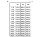
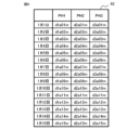
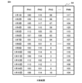
- FIG. 8 shows an example of the inspection result of the dynamic characteristic inspection when there are N probe heads 3 .
- the inspection result 63 shown in FIG. 7 and the inspection result 64 shown in FIG. 8 are examples in which specific numerical values are described.
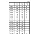
- the inspection result 61 shown in FIG. 5 is the first inspection result for 15 days for a certain inspection item.
- the inspection result 62 shown in FIG. 6 is the m-th inspection result for 15 days for the same inspection item as the inspection result 61 .
- An inspection result 64 shown in FIG. 8 is an inspection result describing the first specific numerical values for 15 days for the same inspection items as the inspection results 61 and 62 .
- the symbol PH and numbers 1, 2, 3 are attached to the probe heads 3a, 3b, 3c, respectively.
- the test results for PH1, PH2, and PH3 on January 1st are d1a0101, d2a0101, and d3a0101, respectively.
- the number on the right side of "d” is the number of the probe head, "a” is the symbol indicating the inspection item, the two-digit number on the right side of "a” indicates the date, and the two-digit number on the right is the inspection date.
- the ordinal number of the test is indicated by m.
- the inspection results in each column of inspection results 61 and 62 are, for example, inspection value data data1 of different semiconductor devices 2 or inspection result data data3 of semiconductor devices 2, respectively. Since the inspection result data data3 includes the inspection value data data1 and the non-defective product determination result data2, the inspection results in each column of the inspection results 61 and 62 can be made into two-dimensional vectors. That is, the inspection result data data3 is represented by, for example, a two-dimensional vector. Incidentally, it is assumed that the inspection result data data3 is written in each column of the inspection results 61 and 62 as appropriate.
- inspection result data data3 of the first probe head 3a that is, PH1 from January 1 to January 15 are d1a0101 to d1a1501, respectively.
- the inspection result data data3 of the second probe head 3b that is, PH2 from January 1 to January 15 are d2a0101 to d2a1501, respectively, and from January 1 to January 15.
- 3 probe head 3c that is, inspection result data data3 of PH3 are d3a0101 to d3a1501, respectively.
- inspection result data data3 of PH1 from January 1 to January 15 are d1a01m to d1a15m, respectively.
- the inspection result data data3 of PH2 from January 1 to January 15 are d2a01m to d2a15m, respectively, and the inspection result data data3 of PH3 from January 1 to January 15 are respectively d3a01m to d3a15m.
- 5 to 7 show an example in which the inspection results are arranged in date order, they may be arranged in order of individually set device numbers or the like.
- the analysis unit 15 analyzes whether the inspection value data data1 in the inspection results of each probe head 3 is normally distributed. If the distribution is not normal, the analysis unit 15 determines that the probe head 3 that is not normally distributed is abnormal.
- the normal distribution analysis for analyzing whether or not the data are normally distributed is determined, for example, from the chi-square values of the target data using the values in the chi-square distribution table at a significance level of 5%.
- a chi-square distribution table is a table of critical values according to statistical degrees of freedom and significance levels. For example, the critical value at 1 degree of freedom and 5% significance level is 3.84.
- the analysis unit 15 outputs an abnormality determination light emission signal sig1 indicating an abnormality determination and an abnormality determination alarm signal sig2 to the warning unit 41 via the control unit 17 .
- the analysis unit 15 performs a second analysis.
- the analysis unit 15 determines that there is no difference between the probe heads 3 from the inspection results of all the probe heads 3 that are performing inspection. or detect significant differences between the probe heads 3 using analysis of variance. Determination of whether or not there is a significant difference in the analysis of variance, that is, determination of significance, is performed at a significance level of 5%.
- FIGS. 5 to 7 show examples in which the target range for significant difference determination is 15 data for each of the three probe heads 3a, 3b, and 3c. In FIG. 8, three probe heads, that is, PH1, PH2, and PH3, are shown as the target range of the significant difference determination performed first. From the second time onwards, it is set within three of PH4 to PHN, which are next to PH3.
- the analysis unit 15 performs a third analysis.
- the analysis unit 15 identifies which probe head 3 has a significant difference compared to other probe heads 3 by multiple comparison.
- the probe heads 3 to be compared are divided. For example, when the number of probe heads 3 is 6, the comparison among the first to third probe heads 3, PH1 to PH3, and the fourth to sixth probe heads 3, PH4 -Compare in PH6.
- the maximum number of subjects for multiple comparisons should be 4 or less.
- the Bonferroni method As a method of multiple comparison, first, it is determined whether there is a significant difference between the probe heads 3 as follows. Multiple comparisons use, for example, the Bonferroni method. For example, consider a case where three probe heads 3 are used for inspection as shown in FIG. In the comparison with three probe heads 3, 5%/3 is the significance level, and between each set of two probe heads 3, namely the first probe head 3a, PH1 and the second probe head 3b, PH2 , between PH1 and the third probe head 3c or PH2, and between PH2 and PH3.
- the analysis unit 15 outputs, via the control unit 17, an abnormality determination light emission signal sig1 and an abnormality determination alarm signal sig2 indicating an abnormality determination of PH2 to the warning unit 41.
- a light emitter 32 provided on the second probe head 3b emits light.
- the method of multiple comparison is not limited to the Bonferroni method. It can be arbitrarily set depending on the data to be analyzed.
- FIGS. 2 to 4 show an example in which the light emitter 32 of the warning unit 41 is provided in each probe head 3 and it is possible to determine which probe head 3 has an abnormality.
- Information on the probe head 3 in which an abnormality has occurred that is, information on the abnormality of the probe head 3 may be displayed on the operation unit 5 .
- the operation unit 5 displays the number of the probe head 3 set so that it can be known which probe head 3 has an abnormality.
- the abnormality information of the probe head 3 displayed on the operation unit 5 does not have to be the probe number.
- the color of the picture may be changed.
- the analysis conditions are, for example, the number of data, the period, the judgment value, and the method for the significant difference judgment by the analysis unit 15 .
- the setting of the number of data includes, for example, setting using the past 100 test results from the latest test result, setting using the past 50 test results, and the like.
- the setting of the period includes, for example, setting using test results for the past 10 days from the latest test result, setting using test results for the past 5 days, and the like.
- the setting of the judgment value is the setting of a reference value for judging whether there is a significant difference, for example, the setting of 5%, the setting of 1%, and the like.
- the setting of the method is the setting of the determination method, and sets whether to use the inspection result data data3 or to use the processed value of the inspection result data data3. For example, there is a setting for judging a significant difference based on the percentage of non-defective products or a ratio of defective products for all inspection items, and a setting for judging a significant difference based on the average value of one inspection item.
- the non-defective product rate or the defective product rate is a ratio based on the non-defective product determination result data2.
- the average value of one inspection item described above is a processed value of the inspection value data data1, and is, for example, an average value of voltage or the like.
- a device inspection method of the device inspection apparatus 50 tests a plurality of semiconductor devices 2 in parallel.
- the device inspection apparatus 50 inspects the semiconductor device 2 (inspection determination procedure).
- a probe head 3 having a probe 33 that contacts the electrode 11 of the semiconductor device 2 is used for each semiconductor device 2 to measure test value data data1 for each semiconductor device 2 .
- the inspection determination unit 18 determines the inspection value data data1 (inspection determination procedure). The inspection determination unit 18 determines whether the semiconductor device 2 is good or defective based on the inspection value data data1.
- the inspection value data data1 and the determination result of step ST02 are stored in the storage unit 16 (storage procedure).
- the storage unit 16 stores the inspection result data data3 including the inspection value data data1 and the judgment result (defective product judgment result data2) of the semiconductor device 2 in step ST02.
- step ST04 analysis is performed by statistical processing in the analysis unit 15 (analysis procedure).
- analysis unit 15 statistical processing is performed based on a plurality of inspection result data data3 existing for each inspection item stored in the storage procedure of step ST03, and a significant difference is found between the plurality of inspection result data data3 for each probe head 3. Whether or not there is a difference is analyzed, and if there is a significant difference, it is determined that the probe head 3 is abnormal.
- a warning is issued using the warning unit 41 in the case of an abnormality determination (warning procedure).
- Device inspection apparatus 50 indicates the result of abnormality determination to warning unit 41 .
- step ST06 it is determined whether or not the semiconductor device 2 to be inspected remains. If there are still objects to be inspected, the process returns to step ST01, and steps ST01 to ST05 are executed. If there are no objects to be inspected, the process ends.
- the functions of the control unit 17, the inspection determination unit 18, and the analysis unit 15 are realized by a processor 98 and a memory 99 provided in the computer 8.
- the control unit 17 , the inspection determination unit 18 , and the analysis unit 15 are implemented by the processor 98 executing programs stored in the memory 99 . Also, multiple processors 98 and multiple memories 99 may cooperate to perform each function.
- the storage unit 16 is an area of the memory 99 that is used by the computer 8 for calculations, which is different from the storage area for programs.
- the control unit 17, the inspection determination unit 18, and the analysis unit 15 are configured by application software.
- the functions of the control unit 17, the inspection determination unit 18, and the analysis unit 15 may be implemented by the processor 98 and the memory 99, and may be configured by devices other than the computer 8.
- Probe abnormalities that misjudge non-defective products as defective also occur in the following cases.
- the semiconductor device 2 is placed in a predetermined location of the device inspection apparatus 50, that is, the concave portion 26 of the housing 1, and the probe head 3 is moved by the moving mechanism 20 such as the air cylinder 23 and the actuator 24. Moved, the probes 33 of the probe head 3 come into contact with the electrodes 11 of the semiconductor device 2 .
- the moving mechanism 20 malfunctions, the probe head 3 collides with the semiconductor device 2 to be inspected, which damages the probe head 3 and causes an abnormality in the probe head 3 such as bending of the probe 33.
- abnormalities in the probe head 3 may be caused by deformation of the tip of the probe 33, adhesion of foreign matter, breakage of the spring in the probe in the case of contact probes, and the like.
- the contact failure between the semiconductor device 2 to be inspected and the probe head 3 does not occur in every measurement, and the contact failure may or may not occur. Therefore, it is difficult to determine whether the semiconductor device 2 is faulty or the probe head 3 is faulty unless some contrivance is made. Furthermore, in an apparatus that inspects a plurality of semiconductor devices 2 in parallel using a plurality of probe heads 3, it is possible to determine which probe head 3 caused the collision between the probe head 3 and the semiconductor device 2 unless some kind of contrivance is made. In some cases, it is difficult to identify the probe head 3 in which an abnormality has occurred.
- the device inspection apparatus 50 of Embodiment 1 analyzes whether there is a significant difference between the plurality of inspection result data data3 for each probe head 3 by statistical processing based on the plurality of inspection result data data3 stored in the storage unit 16. Therefore, at the end of the device inspection of the semiconductor device 2 to be inspected, an abnormality of the probe head 3 can be detected together with the result of the inspection object, that is, the non-defective product determination result data2.
- Abnormalities in the probe head 3 include failures of the probe head 3 and signs of failure. Signs of failure include occasional inspection failures and frequent occurrence of inspection results that differ from normal values.
- One of the causes of a sign of failure is that a foreign object or the like gets caught in the probe 33 of the probe head 3 . This is similar to the attachment of foreign matter to the tip of the probe 33 described above.
- inspection is performed using a monitor sample or the like in order to distinguish whether the failure is caused by the probe head or by the test object. Through this inspection, the cause is isolated, and if the problem is caused by the probe head, the probe head is replaced or repaired. If the probe head 3 has completely failed rather than being a sign of failure, it is conceivable that many defects will occur only in the failed probe head 3 .
- the device inspection apparatus 50 of the first embodiment inspects the semiconductor device 2 to be inspected to the end without stopping the inspection halfway even if an abnormality in the probe head 3 is detected.
- a semiconductor device 2 that has been determined to be defective due to an abnormality in the probe head 3 is subjected to maintenance such as replacement, repair, and foreign matter removal of the probe head 3, and then inspected again.
- the device inspection apparatus 50 and the device inspection method of the first embodiment can perform dynamic characteristic inspection on a plurality of semiconductor devices 2 in parallel, i.e., at the same time, using a plurality of probe heads 3. It is possible to analyze whether an abnormality has occurred. Furthermore, in the device inspection apparatus 50 and the device inspection method of the first embodiment, when an abnormality of the probe head 3 is detected, the operator can be notified by ringing or emitting light from the operation unit 5 and the warning unit 41. . Even when the status of automatic operation is displayed on the operation unit 5, the probe head 3 in which an abnormality has occurred can be visually recognized by causing the light emitter 32 of the warning unit 41 to emit light. The device inspection apparatus 50 and the device inspection method of the first embodiment can arbitrarily set the conditions for analysis, that is, the number of data, the period, the judgment value, and the method. can be adjusted.
- the device inspection apparatus 50 and the device inspection method of Embodiment 1 can detect an abnormality of the probe head 3, including a failure and malfunction of the probe head 3, during inspection. be able to.
- the device inspection apparatus 50 and the device inspection method of the first embodiment can detect an abnormality of the probe head 3 during inspection, so that it is possible to avoid erroneously determining that the semiconductor device 2, which is originally a non-defective product, is defective. can be prevented from being discarded.
- the device inspection apparatus 50 and the device inspection method of the first embodiment can correctly measure the inspection value data data1, so that the correct yield, inspection distribution, and the like can be obtained.
- the device inspection apparatus 50 of Embodiment 1 is a device inspection apparatus that inspects a plurality of semiconductor devices 2 in parallel.
- a plurality of probe heads 3 having probes 33 in contact with electrodes 11 and individually used for each semiconductor device 2, and applying an electric signal for each semiconductor device 2 to a plurality of semiconductor devices 2 to obtain an inspection value for each semiconductor device 2.
- It includes an inspection unit 4 that measures data data1, and an inspection determination unit 18 that determines whether the semiconductor device 2 is good or defective based on the inspection value data data1.
- the device inspection apparatus 50 further includes a storage unit 16 for storing inspection result data data3 including inspection value data data1 and the result of judgment of the semiconductor device 2 (non-defective product judgment result data2); By statistical processing based on a plurality of inspection result data data3 existing for each inspection item, whether there is a significant difference between the plurality of inspection result data data3 for each probe head 3 is analyzed, and if there is a significant difference, the relevant An analysis unit 15 that determines that the probe head 3 is abnormal, and a warning unit 41 that indicates the result of the abnormality determination in the analysis unit 15 that the probe head 3 is abnormal.
- the device inspection apparatus 50 detects a significant difference between the plurality of inspection result data data3 for each probe head 3 by statistical processing based on the plurality of inspection result data data3 recorded in the storage unit 16. Since it is analyzed whether or not there is any, an abnormality of the probe head 3 can be detected together with the result of the inspection target (semiconductor device 2) at the end of the device inspection of the inspection target (semiconductor device 2).
- the device inspection method of the first embodiment is a device inspection method for inspecting a plurality of semiconductor devices 2 in parallel, and includes a plurality of probe heads 3 having a plurality of probes 33 contacting a plurality of electrodes 11 for each semiconductor device 2. and an inspection determination procedure for determining whether the semiconductor device 2 is good or defective based on the inspection value data data1. .
- the device inspection method further includes a storage procedure for storing inspection result data data3 including inspection value data data1 and a judgment result (non-defective product judgment result data2) of the semiconductor device 2; Perform statistical processing based on a plurality of inspection result data data3 existing for each inspection item, analyze whether there is a significant difference between the plurality of inspection result data data3 for each probe head 3, and if there is a significant difference, the probe It includes an analysis procedure for determining that the head 3 is abnormal, and a warning procedure indicating the result of abnormality determination that the probe head 3 is abnormal in the analysis procedure.
- the device inspection method of the first embodiment performs statistical processing based on the plurality of inspection result data data3 recorded in the storage procedure, and finds a significant difference between the plurality of inspection result data data3 for each probe head 3. Since it is analyzed whether or not there is an abnormality, an abnormality of the probe head 3 can be detected together with the result of the inspection target (semiconductor device 2) when the device inspection of the inspection target (semiconductor device 2) is completed.
- FIG. 11 is a diagram showing the configuration of a device inspection apparatus according to the second embodiment
- FIG. 12 is a diagram showing an example of inspection results according to the second embodiment.
- the device inspection apparatus 50 of the second embodiment is different from the device inspection apparatus 50 of the first embodiment in that one semiconductor device 2 is inspected in one inspection.
- the parts different from the device inspection apparatus 50 of the first embodiment will be mainly described.
- FIG. 11 shows an example in which one semiconductor device 2 is mounted on the housing 1 and the probes 33 of one probe head 3 are in contact with the electrodes 11 of the semiconductor device 2 .
- the operation unit 5 and the alarm 6 are omitted in FIG. Only three of the plurality of electrodes 11 in semiconductor device 2 are shown.
- the past inspection result of the single probe head and the latest inspection result are compared to analyze whether there is a significant difference in the latest inspection result. By analyzing in this way, it is detected whether there is an abnormality in the probe head 3 being inspected.
- the probe head In 3 the latest inspection result and the past inspection result are used.
- the inspection results 65 shown in FIG. 12 are the first to m-th inspection results for 15 days for a certain inspection item in the first probe head 3 .
- the inspection results for January 1 are d1a0101 to d1a01m.
- the number on the right side of "d" is the number of the probe head
- "a" is the symbol indicating the inspection item
- the two-digit number on the right side of "a” indicates the date.
- the two digits to the right of indicates the ordinal number of the test. Note that the ordinal number of the m-th inspection is indicated by m.
- the first inspection result data data3 from January 1st to January 15th are d1a0101 to d1a1501, respectively.
- the second inspection result data data3 from January 1 to January 15 are d1a0102 to d1a1502, respectively
- the third inspection result data data3 from January 1 to January 15 are respectively d1a0103. to d1a1503
- m-th inspection result data data3 from January 1 to January 15 are d1a01m to d1a15m, respectively.
- the conditions for performing analysis by the analysis unit 15 are arbitrarily set as part of the operation of the computer 8 from the operation unit 5. be.
- the analysis conditions are, for example, the number of data, the period, the judgment value, and the method for the significant difference judgment by the analysis unit 15 .
- a recess 26 for mounting the semiconductor device 2 is formed on the device mounting surface 25 of the housing 1 . Note that the concave portion 26 is omitted in FIG. 11 .
- the inspection unit 4 applies an electric signal to the semiconductor device 2 and measures inspection value data data1 of the semiconductor device 2 .
- the inspection determination unit 18 determines whether the semiconductor device 2 is a non-defective product or a defective product based on the inspection value data data1.
- the storage unit 16 stores inspection result data data3 including inspection value data data1 and the result of non-defective product determination of the semiconductor device 2, that is, non-defective product determination result data2.
- the analysis unit 15 analyzes whether there is a significant difference between the plurality of test result data data3 by statistical processing based on the plurality of test result data data3 existing for each test item stored in the storage unit 16, and determines whether there is a significant difference. If there is, it is determined that the probe head 3 is abnormal. Determining that the probe head is abnormal is determining that the probe head is abnormal.
- the warning unit 41 indicates the result of the abnormality determination of the probe head 3 by light and/or sound.
- a device inspection method of the device inspection apparatus 50 of the second embodiment inspects one semiconductor device 2 .
- the device inspection apparatus 50 inspects the semiconductor device 2 (inspection determination procedure).
- the test value data data1 of the semiconductor device 2 is measured using the probe head 3 having the probes 33 that contact the electrodes 11 of the semiconductor device 2 .
- the inspection determination unit 18 determines the inspection value data data1 (inspection determination procedure).
- the inspection determination unit 18 determines whether the semiconductor device 2 is good or defective based on the inspection value data data1.
- the inspection value data data1 and the determination result of step ST02 are stored in the storage unit 16 (storage procedure).
- the storage unit 16 stores the inspection result data data3 including the inspection value data data1 and the judgment result (defective product judgment result data2) of the semiconductor device 2 in step ST02.
- step ST04 analysis is performed by statistical processing in the analysis unit 15 (analysis procedure).
- the analysis unit 15 performs statistical processing based on the plurality of inspection result data data3 existing for each inspection item stored in the storage procedure of step ST03, and determines whether there is a significant difference between the plurality of inspection result data data3. If there is a significant difference, it is determined that the probe head 3 is abnormal.
- step ST05 a warning is issued using the warning unit 41 in the case of an abnormality determination (warning procedure).
- Device inspection apparatus 50 indicates the result of abnormality determination to warning unit 41 .
- step ST06 it is determined whether or not the semiconductor device 2 to be inspected remains. If there are still objects to be inspected, the process returns to step ST01, and steps ST01 to ST05 are executed. If there are no objects to be inspected, the process ends.
- the target data for detecting an abnormality in the probe head 3 are the most recent inspection result and the past inspection result of the same probe head 3. Abnormalities in the probe head 3 can be detected even when the devices 2 are not tested in parallel.
- the device inspection apparatus 50 of the second embodiment is a device inspection apparatus for inspecting the semiconductor device 2, and includes the housing 1 on which the semiconductor device 2 is mounted and the probes that contact the electrodes 11 of the semiconductor device 2. 33, an inspection unit 4 that applies an electric signal to the semiconductor device 2 to measure inspection value data data1 of the semiconductor device 2, and a non-defective product or a defective semiconductor device 2 based on the inspection value data data1. and an inspection determination unit 18 for determining whether.
- the device inspection apparatus 50 according to the second embodiment further includes a storage unit 16 for storing inspection result data data3 including inspection value data data1 and the result of judgment of the semiconductor device 2 (non-defective product judgment result data2).
- Statistical processing based on a plurality of inspection result data data3 existing for each inspection item is analyzed to determine whether there is a significant difference between the plurality of inspection result data data3, and if there is a significant difference, the probe head 3 is abnormal.
- the device inspection apparatus 50 of Embodiment 2 analyzes whether there is a significant difference between the plurality of inspection result data data3 by statistical processing based on the plurality of inspection result data data3 recorded in the storage unit 16. Therefore, at the end of the device inspection of the inspection object (semiconductor device 2), the abnormality of the probe head 3 can be detected together with the result of the inspection object (semiconductor device 2).
- a device inspection method is a device inspection method for inspecting a semiconductor device 2, and uses a probe head 3 having probes 33 that come into contact with electrodes 11 of the semiconductor device 2 to obtain inspection value data of the semiconductor device 2. It includes an inspection procedure for measuring data1 and an inspection determination procedure for determining whether the semiconductor device 2 is good or bad based on the inspection value data data1.
- the device inspection method according to the second embodiment further comprises a storage procedure for storing inspection result data data3 including inspection value data data1 and a judgment result (non-defective product judgment result data2) of the semiconductor device 2; Statistical processing is performed based on a plurality of inspection result data data3 existing for each inspection item, and whether or not there is a significant difference between the plurality of inspection result data data3 is analyzed.
- the device inspection method of the second embodiment performs statistical processing based on the plurality of inspection result data data3 recorded in the storage procedure, and analyzes whether there is a significant difference between the plurality of inspection result data data3. Therefore, at the end of the device inspection of the inspection object (semiconductor device 2), the abnormality of the probe head 3 can be detected together with the result of the inspection object (semiconductor device 2).
- FIG. 13 is a diagram showing the configuration of a device inspection apparatus according to the third embodiment.
- a device inspection apparatus 50 according to the third embodiment differs from the device inspection apparatus 50 according to the first embodiment in that the light emitter 32 of the warning section 41 is provided at a different location from the main body 34 of the probe head 3 .
- the parts different from the device inspection apparatus 50 of the first embodiment will be mainly described.
- the light emitters 32 are not arranged on the main body 34 of each probe head 3, and instead the light emitters 32 corresponding to the probe heads 3 are collectively arranged in the light emitter section 9 of the housing 1. I gave an example. Note that the operation unit 5 and the alarm 6 are omitted in FIG.
- the light-emitting unit 9 shown in FIG. 13 is an example of being arranged on the front side in the x direction of the housing 1, and the location on the front side in the x direction is an example of a location that is easily visible to the operator. If there are N probe heads 3 , the light emitter section 9 has N light emitters 32 .
- the light-emitting unit 9 is not limited to the front side of the housing 1 in the x-direction, and may be installed at a place where the device inspection apparatus 50 can easily be visually recognized.
- the probe head 3 may be located in a location that is difficult for the operator to visually recognize. Even in this case, the device inspection apparatus 50 of Embodiment 3 can easily confirm the abnormality of each probe head 3 .
- the light emitter 32 of the warning section 41 may be located in the light emitter section 9 together with the main body 34 of each probe head 3 . If the light emitters 32 are provided at a plurality of locations, the malfunction of each probe head 3 can be quickly confirmed by the one that is easy to confirm.
- the device inspection apparatus 50 of the second embodiment has shown an example in which the light emitter 32 of the warning unit 41 is arranged in the main body 34 of the probe head 3, the device inspection apparatus 50 of the third embodiment , the light-emitting device 32 may be arranged in a place such as the housing 1 that is easily visible to the operator.
Abstract
A device inspection apparatus (50) comprises: a plurality of probe heads (3); an inspection unit (4) that measures inspection value data (data1) for each semiconductor device (2); a storage unit (16) that stores inspection result data (data3) including the inspection value data (data1) and a result (data2) of determination for the semiconductor device (2); and an analysis unit (15) that, by means of statistical processing based on a plurality of inspection result data items (data3) that are present for each inspection item recorded in the storage unit (16), performs an analysis to determine if there is a significant difference between a plurality of inspection result data items (data3) for each probe head (3), and determines that the probe head (3) is abnormal if there is a significant difference.
Description
本願は、デバイス検査装置及びデバイス検査方法に関するものである。
This application relates to a device inspection apparatus and a device inspection method.
半導体ウエハに形成された複数の半導体デバイスは、半導体ウエハにおける全てのプロセスが終了した段階で、プローブを半導体デバイスの電極に接触させて検査が行われる。特許文献1には、半導体ウエハに形成された複数のチップをウエハ状態で並列に検査するプローバ装置及び半導体装置の検査方法が開示されている。チップの検査数が増大するにつれてプローブブロックとチップの電極との間の接触抵抗が増大し、これにより誤って不良品と判定される。特許文献1のプローバ装置を用いた半導体装置の検査方法は、チップの検査数が増大するにつれて誤って不良品と判定されたチップを、再検査により救済するために、再検査対象チップを選択するステップ、複数のプローブブロックを清掃するステップ、複数チップの並列の検査で使用した複数のプローブブロックから再検査に用いる1個のプローブブロックを選択するステップを実行している。
A plurality of semiconductor devices formed on a semiconductor wafer are inspected by bringing probes into contact with the electrodes of the semiconductor devices when all the processes on the semiconductor wafer are completed. Japanese Unexamined Patent Application Publication No. 2002-100001 discloses a prober device and a semiconductor device inspection method for inspecting a plurality of chips formed on a semiconductor wafer in parallel in a wafer state. As the number of chips to be inspected increases, the contact resistance between the probe block and the electrodes of the chip increases, resulting in erroneous determination of defective products. In the semiconductor device inspection method using the prober device of Patent Document 1, as the number of chips to be inspected increases, chips that have been erroneously determined to be defective are reinspected, so that chips to be reinspected are selected. a step of cleaning a plurality of probe blocks; and a step of selecting one probe block to be used for retesting from the plurality of probe blocks used in parallel testing of a plurality of chips.
検査対象の半導体デバイスにおける電気特性等を検査するデバイス検査は、ウエハ状態に限らず分離されたチップ状態で行われる場合もある。検査対象を検査するデバイス検査には、検査対象の電極とプローブヘッドに取り付けられた複数のプローブとを接触させて検査を行う方法がある。プローブヘッドは、複数のプローブを備えており、特許文献1のプローブブロックに相当するものである。このデバイス検査の際に、検査対象とプローブとが接触不良を発生させるようなプローブの異常が発生する場合がある。このようなプローブの異常が発生した場合には、良品を不良品と誤判定する問題がある。
The device inspection, which inspects the electrical characteristics, etc. of the semiconductor device to be inspected, is not limited to the wafer state, but may be performed in the separated chip state. 2. Description of the Related Art Device inspection for inspecting an object to be inspected includes a method of inspecting by bringing electrodes of the object to be inspected into contact with a plurality of probes attached to a probe head. The probe head has a plurality of probes and corresponds to the probe block of Patent Document 1. During this device inspection, there is a case where an abnormality occurs in the probe that causes contact failure between the inspection object and the probe. When such an abnormality occurs in the probe, there is a problem that a non-defective product is erroneously determined as a defective product.
特許文献1のプローバ装置を用いた半導体装置の検査方法は、不良品判定されたチップに対して、ウエハの全チップを検査した後に当該チップを含むウエハにおける検査結果に基づいて選択されかつ清掃されたプローブブロックを用いて、ウエハを交換することなく再検査を行っている。再検査のプローブブロックは、並列の検査で使用したプローブブロック毎の良品率が算出され、このプローブブロック毎の良品率が最大となるプローブブロックが選択される。特許文献1のプローバ装置を用いた半導体装置の検査方法は、誤判定を低減することはできる。しかし、特許文献1のプローバ装置を用いた半導体装置の検査方法は、ウエハの全チップを検査した後に読み込んだ検査結果に基づいてプローブブロック毎の良品率を算出するので、再検査前の検査すなわち初回の検査においてプローブブロック(プローブヘッド)の異常を検出することができない。
In the method of testing a semiconductor device using a prober apparatus disclosed in Patent Document 1, all chips on a wafer are tested for chips that have been determined to be defective, and then selected and cleaned based on the test results of the wafer including the chips. A new probe block is used to perform re-inspection without replacing the wafer. As for the probe blocks for re-inspection, the non-defective product rate for each probe block used in the parallel inspection is calculated, and the probe block with the maximum non-defective product rate for each probe block is selected. The semiconductor device inspection method using the prober apparatus disclosed in Patent Document 1 can reduce erroneous determinations. However, in the semiconductor device inspection method using the prober apparatus of Patent Document 1, the non-defective product rate for each probe block is calculated based on the inspection results read after all the chips on the wafer have been inspected. Abnormalities in the probe block (probe head) cannot be detected in the first inspection.
本願明細書に開示される技術は、検査対象のデバイス検査の終了の際に、検査対象の結果と共にプローブヘッドの異常を検出することを目的とする。
The technology disclosed in the specification of the present application aims to detect an abnormality of the probe head together with the result of the inspection target when the inspection of the device to be inspected ends.
本願明細書に開示される一例のデバイス検査装置は、複数の半導体デバイスを搭載する筐体と、半導体デバイスの電極に接触するプローブを有し、半導体デバイス毎に個別に用いる複数のプローブヘッドと、複数の半導体デバイスに半導体デバイス毎の電気信号を印加して半導体デバイス毎の検査値データを測定する検査部と、検査値データに基づいて、半導体デバイスの良品か不良品かの判定を行う検査判定部と、を備えている。本願明細書に開示される一例のデバイス検査装置は、更に、検査値データ及び半導体デバイスの判定の結果を含む検査結果データを記憶する記憶部と、記憶部に記憶された検査項目毎に存在する複数の検査結果データに基づいた統計処理により、プローブヘッド毎の複数の検査結果データ間に有意差があるかを解析し、有意差がある場合に当該プローブヘッドが異常であると判定する解析部と、解析部におけるプローブヘッドが異常であるとの異常判定の結果を示す警告部と、を備えている。
An example device inspection apparatus disclosed in the specification of the present application includes a housing for mounting a plurality of semiconductor devices, a plurality of probe heads that have probes that contact electrodes of the semiconductor devices, and is used individually for each semiconductor device, An inspection unit that applies an electrical signal for each semiconductor device to a plurality of semiconductor devices and measures inspection value data for each semiconductor device, and an inspection judgment that determines whether the semiconductor device is a non-defective product or a defective product based on the inspection value data. and An example of the device inspection apparatus disclosed in the present specification further includes a storage unit for storing inspection result data including inspection value data and semiconductor device judgment results, and each inspection item stored in the storage unit. Analysis unit that analyzes whether there is a significant difference between multiple inspection result data for each probe head by statistical processing based on multiple inspection result data, and determines that the probe head is abnormal when there is a significant difference and a warning unit that indicates the result of abnormality determination that the probe head is abnormal in the analysis unit.
本願明細書に開示される一例のデバイス検査装置は、記憶部に記憶された複数の検査結果データに基づいた統計処理によりプローブヘッド毎の複数の検査結果データ間に有意差があるかを解析するので、検査対象のデバイス検査の終了の際に、検査対象の結果と共にプローブヘッドの異常を検出することができる。
An example device inspection apparatus disclosed in the present specification analyzes whether there is a significant difference between a plurality of inspection result data for each probe head by statistical processing based on a plurality of inspection result data stored in a storage unit. Therefore, it is possible to detect an abnormality of the probe head together with the result of the inspection target at the end of the inspection of the device to be inspected.
実施の形態1.
図1は、実施の形態1に係るデバイス検査装置の構成を示す図である。図2は図1の筐体に搭載された検査対象及びプローブヘッドを示す図であり、図3は図2のプローブヘッド及び検査対象を示す図である。図4は、図2のプローブヘッドの移動機構を示す図である。図5~図8は、それぞれ実施の形態1に係る検査結果の一例を示す図である。図9は実施の形態1に係るデバイス検査方法を示すフローチャートであり、図10は図1の制御部、検査判定部、解析部の機能を実現するハードウェア構成例を示す図である。実施の形態1のデバイス検査装置50は、検査対象である半導体デバイス2を搭載する筐体1、複数のプローブ33を有しており少なとも1個のプローブヘッド3、半導体デバイス2に電気信号を印加して半導体デバイス2の検査値データdata1を測定する検査部4、検査部4を制御すると共に半導体デバイス2の良品判定及びプローブヘッド3の異常判定を行うコンピュータ8、プローブヘッド3の異常判定の結果を示す警告部41、プローブヘッド3を移動する移動機構20、コンピュータ8及び移動機構20を操作する操作部5を備えている。操作部5は、例えばタッチパネル式のディスプレイである。Embodiment 1.
FIG. 1 is a diagram showing the configuration of a device inspection apparatus according toEmbodiment 1. FIG. FIG. 2 is a diagram showing the test object and the probe head mounted on the housing of FIG. 1, and FIG. 3 is a diagram showing the probe head and the test object of FIG. 4 is a diagram showing a moving mechanism of the probe head of FIG. 2. FIG. 5 to 8 are diagrams showing examples of inspection results according to the first embodiment, respectively. FIG. 9 is a flow chart showing the device inspection method according to the first embodiment, and FIG. 10 is a diagram showing a hardware configuration example realizing the functions of the control unit, inspection determination unit, and analysis unit shown in FIG. A device inspection apparatus 50 of Embodiment 1 has a housing 1 for mounting a semiconductor device 2 to be inspected, a plurality of probes 33 , and at least one probe head 3 and an electrical signal to the semiconductor device 2 . An inspection unit 4 that measures inspection value data data1 of the semiconductor device 2 by applying voltage, a computer 8 that controls the inspection unit 4 and performs non-defective determination of the semiconductor device 2 and abnormality determination of the probe head 3, and abnormality determination of the probe head 3. A warning unit 41 for indicating a result, a moving mechanism 20 for moving the probe head 3, and an operation unit 5 for operating the computer 8 and the moving mechanism 20 are provided. The operation unit 5 is, for example, a touch panel display.
図1は、実施の形態1に係るデバイス検査装置の構成を示す図である。図2は図1の筐体に搭載された検査対象及びプローブヘッドを示す図であり、図3は図2のプローブヘッド及び検査対象を示す図である。図4は、図2のプローブヘッドの移動機構を示す図である。図5~図8は、それぞれ実施の形態1に係る検査結果の一例を示す図である。図9は実施の形態1に係るデバイス検査方法を示すフローチャートであり、図10は図1の制御部、検査判定部、解析部の機能を実現するハードウェア構成例を示す図である。実施の形態1のデバイス検査装置50は、検査対象である半導体デバイス2を搭載する筐体1、複数のプローブ33を有しており少なとも1個のプローブヘッド3、半導体デバイス2に電気信号を印加して半導体デバイス2の検査値データdata1を測定する検査部4、検査部4を制御すると共に半導体デバイス2の良品判定及びプローブヘッド3の異常判定を行うコンピュータ8、プローブヘッド3の異常判定の結果を示す警告部41、プローブヘッド3を移動する移動機構20、コンピュータ8及び移動機構20を操作する操作部5を備えている。操作部5は、例えばタッチパネル式のディスプレイである。
FIG. 1 is a diagram showing the configuration of a device inspection apparatus according to
図2では、複数の半導体デバイス2を並列に検査するデバイス検査装置50の例を示した。図4では、3個の半導体デバイス2を並列に検査する場合のデバイス検査装置50における移動機構20を示した。移動機構20は、複数のプローブヘッド3a、3b、3cが固定されたヘッド固定板21を筐体1のデバイス搭載面25に平行な方向であるx方向に移動するアクチュエータ24、ヘッド固定板21を筐体1のデバイス搭載面25に垂直な方向であるy方向に移動するエアシリンダ23を備えている。y方向はx方向に垂直である。図4では、x方向は紙面の手前側と奥側との方向であり、y方向はデバイス搭載面25に近い側と遠い側との方向である。移動機構20は、エアシリンダ23が固定されたエアシリンダ固定板22を備えている。エアシリンダ23は、複数のプローブヘッド3a、3b、3cが固定されたヘッド固定板21を保持すると共にy方向にヘッド固定板21を移動する。エアシリンダ固定板22はアクチュエータ24によりx方向に移動する。なお、N個の半導体デバイス2を並列に検査するデバイス検査装置50における移動機構20も図4に示した移動機構20と同様である。ヘッド固定板21にN個のプローブヘッド3が固定される。
FIG. 2 shows an example of a device inspection apparatus 50 that inspects a plurality of semiconductor devices 2 in parallel. FIG. 4 shows the moving mechanism 20 in the device inspection apparatus 50 when inspecting three semiconductor devices 2 in parallel. The moving mechanism 20 includes an actuator 24 that moves the head fixing plate 21 to which the plurality of probe heads 3a, 3b, and 3c are fixed in the x direction parallel to the device mounting surface 25 of the housing 1, and the head fixing plate 21. It has an air cylinder 23 that moves in the y direction, which is the direction perpendicular to the device mounting surface 25 of the housing 1 . The y-direction is perpendicular to the x-direction. In FIG. 4, the x direction is the direction toward the front side and the back side of the paper, and the y direction is the direction toward the side closer to and farther from the device mounting surface 25 . The moving mechanism 20 has an air cylinder fixing plate 22 to which an air cylinder 23 is fixed. The air cylinder 23 holds the head fixing plate 21 to which the plurality of probe heads 3a, 3b, and 3c are fixed and moves the head fixing plate 21 in the y direction. The air cylinder fixed plate 22 is moved in the x direction by an actuator 24 . The moving mechanism 20 in the device inspection apparatus 50 for inspecting N semiconductor devices 2 in parallel is also the same as the moving mechanism 20 shown in FIG. N probe heads 3 are fixed to the head fixing plate 21 .
検査対象である半導体デバイス2は、例えば赤外線センサである。赤外線センサは、ガラスエポキシ基板等の基板に複数の部品が搭載されてモジュールである。赤外線センサは、フォトダイオードにより形成された温度センサを有する赤外線センサチップ、赤外線センサチップを制御する制御回路又は制御IC(Integrated Circuit)、コンデンサ等の電子部品を備えている。図2~図4では半導体デバイス2における複数の電極11のうち3個のみを示した。電極11は、例えばフォトダイオードのアノード、カソード、制御回路の入出力電極等である。半導体デバイス2の電極11は、例えばガラスエポキシ基板等の基板に形成されている。プローブヘッド3と検査対象の半導体デバイス2とは一対一に対応しており、プローブヘッド3の数と検査対象の半導体デバイス2の数は同数である。
The semiconductor device 2 to be inspected is, for example, an infrared sensor. An infrared sensor is a module in which a plurality of components are mounted on a substrate such as a glass epoxy substrate. The infrared sensor includes an infrared sensor chip having a temperature sensor formed by a photodiode, a control circuit or control IC (Integrated Circuit) for controlling the infrared sensor chip, and electronic components such as a capacitor. 2 to 4 show only three of the plurality of electrodes 11 in the semiconductor device 2. FIG. The electrode 11 is, for example, an anode or cathode of a photodiode, an input/output electrode of a control circuit, or the like. The electrodes 11 of the semiconductor device 2 are formed on a substrate such as a glass epoxy substrate. The probe heads 3 and the semiconductor devices 2 to be inspected are in one-to-one correspondence, and the number of probe heads 3 and the number of semiconductor devices 2 to be inspected are the same.
プローブヘッド3は、本体34、本体34に固定された複数のプローブ33、複数のプローブ33にそれぞれ接続されたケーブル31を備えている。図2~図4では、プローブヘッド3の本体34に発光器32が設けられているので、発光器32を発光させる信号を伝送するケーブル31も存在する。なお、ケーブル31の数は図示された数に限定されない。図4ではプローブヘッド3、半導体デバイス2がそれぞれ3個の場合を示しており、3個のプローブヘッド3を区別するために3a、3b、3cの符号を付している。同様に、3個の半導体デバイス2を区別するために2a、2b、2cの符号を付しており、3個の発光器32を区別するために32a、32b、32cの符号を付している。すなわち、プローブヘッドの符号は、総括的に3を用い、区別して説明する場合に3a、3b、3cを用いる。半導体デバイスの符号は、総括的に2を用い、区別して説明する場合に2a、2b、2cを用いる。発光器の符号は、総括的に32を用い、区別して説明する場合に32a、32b、32cを用いる。
The probe head 3 includes a main body 34, a plurality of probes 33 fixed to the main body 34, and cables 31 connected to the plurality of probes 33, respectively. 2 to 4, since the light emitter 32 is provided on the main body 34 of the probe head 3, there is also a cable 31 for transmitting a signal for causing the light emitter 32 to emit light. Note that the number of cables 31 is not limited to the illustrated number. FIG. 4 shows a case in which there are three probe heads 3 and three semiconductor devices 2, and the three probe heads 3 are denoted by 3a, 3b, and 3c to distinguish them. Similarly, reference numerals 2a, 2b, and 2c are attached to distinguish the three semiconductor devices 2, and reference numerals 32a, 32b, and 32c are attached to distinguish the three light emitters 32. . That is, the reference numerals for the probe heads are 3 in general, and 3a, 3b, and 3c when distinguishing them. The reference numerals for semiconductor devices are 2 in general, and 2a, 2b, and 2c when distinguishing them. The reference numerals for the light emitters are 32 in general, and 32a, 32b, and 32c when distinguishing them.
筐体1のデバイス搭載面25には、半導体デバイス2を載せるための凹部26が形成されている。凹部26に搭載される前の複数の半導体デバイス2は図示しないトレイに配置されており、図示しないデバイス検査装置50のデバイス移動機構によりトレイから凹部26に半導体デバイス2が移動される。検査後には、デバイス検査装置50のデバイス移動機構により凹部26から図示しない他のトレイに半導体デバイス2が移動される。デバイス移動機構は、操作部5により操作される。なお、半導体デバイス2の凹部26への移動、半導体デバイス2の凹部26からの移動は手動で行ってもよい。
A recess 26 for mounting the semiconductor device 2 is formed on the device mounting surface 25 of the housing 1 . A plurality of semiconductor devices 2 are placed on a tray (not shown) before being mounted in the recess 26 , and the semiconductor devices 2 are moved from the tray to the recess 26 by a device moving mechanism of the device inspection apparatus 50 (not shown). After the inspection, the device moving mechanism of the device inspection apparatus 50 moves the semiconductor device 2 from the concave portion 26 to another tray (not shown). The device moving mechanism is operated by the operating section 5 . The movement of the semiconductor device 2 to the concave portion 26 and the movement of the semiconductor device 2 from the concave portion 26 may be performed manually.
検査部4は、複数の半導体デバイス2に半導体デバイス2毎の電気信号を印加して半導体デバイス2毎の検査値データdata1を測定する。より具体的には、検査部4は、半導体デバイス2の電極11に直流電圧、制御信号等の電気信号をプローブ33を介して供給する電流電圧源29、コンピュータ8と通信するアダプタ28等を備えている。アダプタ28は、コンピュータ8からの制御信号sigcに基づいて半導体デバイス2の検査を実行し、測定された検査値データdata1をコンピュータ8に出力する。コンピュータ8は、制御部17、検査判定部18、記憶部16、解析部15を備えている。制御部17は、制御信号sigcを検査部4に出力し、検査部4を制御する。検査部4は、制御信号sigcに基づいて半導体デバイス2を動作させ、動作させた結果を検査値データdata1としてコンピュータ8に出力する。半導体デバイス2の検査の際に、検査項目に従って半導体デバイス2にデータ書き込み、電流電圧源29による電圧印加が検査部4により行われる。
The inspection unit 4 applies an electric signal for each semiconductor device 2 to a plurality of semiconductor devices 2 and measures inspection value data data1 for each semiconductor device 2 . More specifically, the inspection unit 4 includes a current/voltage source 29 that supplies electrical signals such as DC voltages and control signals to the electrodes 11 of the semiconductor device 2 via the probes 33, an adapter 28 that communicates with the computer 8, and the like. ing. The adapter 28 inspects the semiconductor device 2 based on the control signal sigc from the computer 8 and outputs measured inspection value data data1 to the computer 8 . The computer 8 includes a control section 17 , an inspection determination section 18 , a storage section 16 and an analysis section 15 . The control unit 17 outputs the control signal sigc to the inspection unit 4 to control the inspection unit 4 . The inspection unit 4 operates the semiconductor device 2 based on the control signal sigc, and outputs the result of the operation to the computer 8 as inspection value data data1. When inspecting the semiconductor device 2 , data is written to the semiconductor device 2 according to inspection items, and voltage is applied by the current/voltage source 29 by the inspection unit 4 .
検査判定部18は、検査値データdata1に基づいて、半導体デバイス2の良品か不良品かの判定すなわち良品判定を行う。記憶部16は、検査値データdata1及び半導体デバイス2の良品判定の結果すなわち良品判定結果data2を含む検査結果データdata3を記憶する。解析部15は、記憶部16に記憶された検査項目毎に存在する複数の検査結果データdata3に基づいた統計処理により、プローブヘッド3毎の複数の検査結果データdata3間に有意差があるかを解析し、有意差がある場合に当該プローブヘッドが異常であると判定する。有意差は、統計上あるいは統計処理で認められる差である。プローブヘッドが異常であるとの判定は、プローブヘッドの異常判定である。
Based on the inspection value data data1, the inspection determination unit 18 determines whether the semiconductor device 2 is a non-defective product or a defective product, that is, performs non-defective product determination. The storage unit 16 stores inspection result data data3 including inspection value data data1 and the result of non-defective product determination of the semiconductor device 2, that is, non-defective product determination result data2. The analysis unit 15 performs statistical processing based on the plurality of inspection result data data3 existing for each inspection item stored in the storage unit 16 to determine whether there is a significant difference between the plurality of inspection result data data3 for each probe head 3. The probe head is determined to be abnormal when it is analyzed and there is a significant difference. A significant difference is a difference recognized statistically or by statistical processing. Determining that the probe head is abnormal is determining that the probe head is abnormal.
警告部41は、例えばプローブヘッド3毎に設けられた異常判定の結果を光で示す発光器32、異常判定とされたプローブヘッド3が少なくも1個ある場合に音で示すアラーム6を備えている。プローブヘッド3が異常判定とされた場合に、当該プローブヘッド3に対応した発光器32が発光する。プローブヘッド3が異常判定とされない場合すなわち正常な場合には、当該プローブヘッド3に対応した発光器32は発光しない。解析部15にてプローブヘッド3の異常判定がされた場合には、制御部17を介して異常判定を示す異常判定発光信号sig1、異常判定アラーム信号sig2が警告部41に出力される。異常判定発光信号sig1はプローブヘッド3毎に出力される。発光器32は、異常判定発光信号sig1が異常判定を示す場合は発光し、異常判定発光信号sig1が異常判定を示さない場合は発光しない。アラーム6は、異常判定アラーム信号sig2が異常判定を示す場合は鳴動し、異常判定アラーム信号sig2が異常判定を示さない場合は鳴動しない。アラーム6は、検査部4、操作部5、筐体1、デバイス検査装置50が配置された部屋内等に設置されている。デバイス検査装置50のオペレータは、操作部5からコンピュータ8の操作の一部として解析部15にて解析を行う条件を設定する。
The warning unit 41 includes, for example, a light emitter 32 that is provided for each probe head 3 and indicates the result of abnormality determination by light, and an alarm 6 that indicates by sound when at least one probe head 3 is determined to be abnormal. there is When the probe head 3 is determined to be abnormal, the light emitter 32 corresponding to the probe head 3 emits light. When the probe head 3 is not determined to be abnormal, that is, when it is normal, the light emitter 32 corresponding to the probe head 3 does not emit light. When the analysis unit 15 determines that the probe head 3 is abnormal, an abnormality determination light emission signal sig1 and an abnormality determination alarm signal sig2 indicating the abnormality determination are output to the warning unit 41 via the control unit 17 . An abnormality determination light emission signal sig1 is output for each probe head 3 . The light emitter 32 emits light when the abnormality determination light emission signal sig1 indicates an abnormality determination, and does not emit light when the abnormality determination light emission signal sig1 does not indicate an abnormality determination. Alarm 6 sounds when abnormality determination alarm signal sig2 indicates abnormality determination, and does not sound when abnormality determination alarm signal sig2 does not indicate abnormality determination. The alarm 6 is installed in a room or the like in which the inspection unit 4, the operation unit 5, the housing 1, and the device inspection apparatus 50 are arranged. An operator of the device inspection apparatus 50 sets conditions for performing analysis by the analysis section 15 as part of the operation of the computer 8 from the operation section 5 .
デバイス検査装置50は、半導体デバイス2に電気信号を与えて半導体デバイス2の電気特性を検査する。ここでは、電気信号を与えて半導体デバイス2を動作させて半導体デバイス2の電気特性を検査することを動的特性検査と呼ぶことにする。半導体デバイス2の機能を発揮させる電気信号を与えずに、半導体デバイス2における抵抗等の特性を検査することを静的特性検査と呼ぶことにする。半導体デバイス2が赤外線センサの場合、動的特性検査の一例は、黒体炉から放射された輻射熱による赤外線センサが検出する画像データに基づいて赤外線センサの調整を行う検査である。赤外線センサは入射する赤外線量の変化によって出力電圧が変化し、動的特性検査はその変化量の度合いが規格範囲内であるかを検査する。黒体炉は、赤外線センサの検出面に対向するようにデバイス検査装置50に配置され、一定の温度の輻射熱を放射する。赤外線センサの調整を行いながら所望の特性が得られる場合は良品と判定する。調整しきれずに所望の特性が得られない場合は不良品と判定する。
The device inspection apparatus 50 applies electrical signals to the semiconductor device 2 to inspect the electrical characteristics of the semiconductor device 2 . Here, inspecting the electrical characteristics of the semiconductor device 2 by applying an electrical signal to operate the semiconductor device 2 is called a dynamic characteristics inspection. Inspecting the characteristics such as the resistance of the semiconductor device 2 without applying an electrical signal for the function of the semiconductor device 2 is called a static characteristic inspection. When the semiconductor device 2 is an infrared sensor, an example of the dynamic characteristic inspection is an inspection for adjusting the infrared sensor based on image data detected by the infrared sensor using radiant heat emitted from a black body furnace. The infrared sensor changes its output voltage according to changes in the amount of incident infrared rays, and the dynamic characteristic inspection checks whether the degree of the change is within the standard range. The blackbody furnace is arranged in the device inspection apparatus 50 so as to face the detection surface of the infrared sensor, and radiates radiant heat at a constant temperature. If the desired characteristics are obtained while adjusting the infrared sensor, the product is determined to be non-defective. If the desired characteristics cannot be obtained due to insufficient adjustment, the product is determined to be defective.
デバイス検査装置50は、各検査項目の動的特性検査において、半導体デバイス2に電圧を印加しても電流が流れない場合は半導体デバイス2が不良品であると判定する。不良品の判定は、検査判定部18が行う。デバイス検査装置50の検査判定部18は、半導体デバイス2の検査値データdata1が判定基準を満たす場合に半導体デバイス2が良品であると判定する。半導体デバイス2の良品か不良品かの判定結果すなわち良品判定結果data2は、検査値データdata1と共に記憶部16に記憶される。解析部15は、検査値データdata1及び良品判定結果data2を含む検査結果データdata3が記憶部16に記憶される度に、検査結果データdata3に基づいた統計処理による解析を行う。
The device inspection apparatus 50 determines that the semiconductor device 2 is defective if no current flows even if a voltage is applied to the semiconductor device 2 in the dynamic characteristic inspection for each inspection item. Defective product determination is performed by the inspection determination unit 18 . The inspection determination unit 18 of the device inspection apparatus 50 determines that the semiconductor device 2 is non-defective when the inspection value data data1 of the semiconductor device 2 satisfies the determination criteria. The determination result as to whether the semiconductor device 2 is good or bad, that is, the good product determination result data2 is stored in the storage unit 16 together with the inspection value data data1. Every time inspection result data data3 including inspection value data data1 and non-defective product determination result data2 is stored in storage unit 16, analysis unit 15 performs analysis by statistical processing based on inspection result data data3.
次に、解析部15が実行する解析方法を説明する。プローブヘッド3が3個の場合の動的特性検査の検査結果の一例を図5~図7に示した。プローブヘッド3がN個の場合の動的特性検査の検査結果の一例を図8に示した。図7に示した検査結果63及び図8に示した検査結果64は、具体的な数値が記載された例である。図5に示した検査結果61は、ある検査項目における15日分の1回目の検査結果である。図6に示した検査結果62は、検査結果61と同じ検査項目における15日分のm回目の検査結果である。図7に示した検査結果63は、検査結果61、62と同じ検査項目における15日分の1回目の具体的な数値を記載した検査結果である。図8に示した検査結果64は、検査結果61、62と同じ検査項目における15日分の1回目の具体的な数値を記載した検査結果である。
Next, the analysis method executed by the analysis unit 15 will be described. An example of the inspection results of the dynamic characteristic inspection when there are three probe heads 3 is shown in FIGS. 5 to 7. FIG. FIG. 8 shows an example of the inspection result of the dynamic characteristic inspection when there are N probe heads 3 . The inspection result 63 shown in FIG. 7 and the inspection result 64 shown in FIG. 8 are examples in which specific numerical values are described. The inspection result 61 shown in FIG. 5 is the first inspection result for 15 days for a certain inspection item. The inspection result 62 shown in FIG. 6 is the m-th inspection result for 15 days for the same inspection item as the inspection result 61 . An inspection result 63 shown in FIG. 7 is an inspection result describing the first specific numerical values for 15 days for the same inspection items as the inspection results 61 and 62 . An inspection result 64 shown in FIG. 8 is an inspection result describing the first specific numerical values for 15 days for the same inspection items as the inspection results 61 and 62 .
検査結果61、62、63では、プローブヘッド3a、3b、3c毎にそれぞれ記号PH及び番号1、2、3を付している。1月1日の1回目におけるPH1、PH2、PH3の検査結果は、それぞれd1a0101、d2a0101、d3a0101である。「d」の右側の数字がプローブヘッドの番号であり、「a」が検査項目を示す記号であり、「a」の右側の2桁の数字が日を示し、その右側の2桁が検査の序数を示している。なお、検査結果62では、検査の序数はmで示している。検査結果61、62の各欄の検査結果は、例えばそれぞれ異なる半導体デバイス2の検査値データdata1、又は半導体デバイス2の検査結果データdata3である。検査結果データdata3の場合は、検査値データdata1及び良品判定結果data2を含むので、検査結果61、62の各欄の検査結果は2次元ベクトルにすればよい。すなわち検査結果データdata3は、例えば2次元ベクトルで表記される。なお、適宜、検査結果61、62の各欄に検査結果データdata3が記載されているとして説明する。
In the inspection results 61, 62, 63, the symbol PH and numbers 1, 2, 3 are attached to the probe heads 3a, 3b, 3c, respectively. The test results for PH1, PH2, and PH3 on January 1st are d1a0101, d2a0101, and d3a0101, respectively. The number on the right side of "d" is the number of the probe head, "a" is the symbol indicating the inspection item, the two-digit number on the right side of "a" indicates the date, and the two-digit number on the right is the inspection date. Indicates an ordinal number. In the test result 62, the ordinal number of the test is indicated by m. The inspection results in each column of inspection results 61 and 62 are, for example, inspection value data data1 of different semiconductor devices 2 or inspection result data data3 of semiconductor devices 2, respectively. Since the inspection result data data3 includes the inspection value data data1 and the non-defective product determination result data2, the inspection results in each column of the inspection results 61 and 62 can be made into two-dimensional vectors. That is, the inspection result data data3 is represented by, for example, a two-dimensional vector. Incidentally, it is assumed that the inspection result data data3 is written in each column of the inspection results 61 and 62 as appropriate.
検査結果61において、1月1日~1月15日における第1のプローブヘッド3aすなわちPH1の検査結果データdata3は、それぞれd1a0101~d1a1501である。同様に、検査結果61において、1月1日~1月15日における第2のプローブヘッド3bすなわちPH2の検査結果データdata3はそれぞれd2a0101~d2a1501であり、1月1日~1月15日における第3のプローブヘッド3cすなわちPH3の検査結果データdata3はそれぞれd3a0101~d3a1501である。検査結果62において、1月1日~1月15日におけるPH1の検査結果データdata3は、それぞれd1a01m~d1a15mである。同様に、検査結果62において、1月1日~1月15日におけるPH2の検査結果データdata3はそれぞれd2a01m~d2a15mであり、1月1日~1月15日におけるPH3の検査結果データdata3はそれぞれd3a01m~d3a15mである。なお、検査結果は図5~図7では日付順に並んでいる例を示したが、個別に設定されたデバイス番号順等でもよい。
In the inspection result 61, inspection result data data3 of the first probe head 3a, that is, PH1 from January 1 to January 15 are d1a0101 to d1a1501, respectively. Similarly, in the inspection result 61, the inspection result data data3 of the second probe head 3b, that is, PH2 from January 1 to January 15 are d2a0101 to d2a1501, respectively, and from January 1 to January 15. 3 probe head 3c, that is, inspection result data data3 of PH3 are d3a0101 to d3a1501, respectively. In the inspection result 62, inspection result data data3 of PH1 from January 1 to January 15 are d1a01m to d1a15m, respectively. Similarly, in the inspection results 62, the inspection result data data3 of PH2 from January 1 to January 15 are d2a01m to d2a15m, respectively, and the inspection result data data3 of PH3 from January 1 to January 15 are respectively d3a01m to d3a15m. 5 to 7 show an example in which the inspection results are arranged in date order, they may be arranged in order of individually set device numbers or the like.
まず、第一解析として、解析部15は、各プローブヘッド3の検査結果における検査値データdata1が正規分布しているかを解析する。解析部15は、正規分布でない場合、正規分布していないプローブヘッド3を異常と判定する。正規分布しているかを解析する正規分布解析は、例えば対象データのカイ二乗値から、有意水準が5%におけるカイ二乗分布表の値で判定する。カイ二乗分布表は、統計上の自由度と有意水準とによる臨界値を表にまとめたものである。例えば、自由度が1で有意水準が5%における臨界値は3.84である。図7の検査結果63において、第3のプローブヘッド3cすなわちPH3は、正規分布でないと判定される。この場合、解析部15は、制御部17を介して異常判定を示す異常判定発光信号sig1、異常判定アラーム信号sig2を警告部41に出力する。
First, as a first analysis, the analysis unit 15 analyzes whether the inspection value data data1 in the inspection results of each probe head 3 is normally distributed. If the distribution is not normal, the analysis unit 15 determines that the probe head 3 that is not normally distributed is abnormal. The normal distribution analysis for analyzing whether or not the data are normally distributed is determined, for example, from the chi-square values of the target data using the values in the chi-square distribution table at a significance level of 5%. A chi-square distribution table is a table of critical values according to statistical degrees of freedom and significance levels. For example, the critical value at 1 degree of freedom and 5% significance level is 3.84. In the inspection result 63 of FIG. 7, it is determined that the third probe head 3c, ie PH3, does not have a normal distribution. In this case, the analysis unit 15 outputs an abnormality determination light emission signal sig1 indicating an abnormality determination and an abnormality determination alarm signal sig2 to the warning unit 41 via the control unit 17 .
次に、解析部15は第二解析を行う。第二解析として、解析部15は、プローブヘッド3の検査結果における検査値データdata1が正規分布していれば、検査を実行している全プローブヘッド3の検査結果からプローブヘッド3間に違いがあるか、プローブヘッド3間の有意差を分散分析法を用いて検出する。分散分析法における有意差があるか無いかの判定すなわち有意差判定は、有意水準は5%で行う。図5~図7では、有意差判定の対象範囲は、3個のプローブヘッド3a、3b、3cの各15個のデータとなっている例を示した。図8では、初めに行う有意差判定の対象範囲として3個のプローブヘッドすなわちPH1、PH2、PH3を示した。2回目以降は、PH3の次であるPH4~PHNのうち3個以内で設定される。
Next, the analysis unit 15 performs a second analysis. As the second analysis, if the inspection value data data1 in the inspection results of the probe heads 3 are normally distributed, the analysis unit 15 determines that there is no difference between the probe heads 3 from the inspection results of all the probe heads 3 that are performing inspection. or detect significant differences between the probe heads 3 using analysis of variance. Determination of whether or not there is a significant difference in the analysis of variance, that is, determination of significance, is performed at a significance level of 5%. FIGS. 5 to 7 show examples in which the target range for significant difference determination is 15 data for each of the three probe heads 3a, 3b, and 3c. In FIG. 8, three probe heads, that is, PH1, PH2, and PH3, are shown as the target range of the significant difference determination performed first. From the second time onwards, it is set within three of PH4 to PHN, which are next to PH3.
分散分析法により何れかのプローブヘッド3に有意差があることが判った場合は、解析部15は第三解析を行う。第三解析として、解析部15は、多重比較によりどのプローブヘッド3が他のプローブヘッド3と比べて有意差があるかを特定する。なお、図8の検査結果65のようにプローブヘッド3の数がN個であり、プローブヘッド3の数が多い場合は比較するプローブヘッド3を分ける。例えばプローブヘッド3の数が6個の場合は、第1のプローブヘッド~第3のプローブヘッド3すなわちPH1~PH3の中での比較と、第4のプローブヘッド~第6のプローブヘッド3すなわちPH4~PH6の中での比較を行う。多重比較の対象とする最大数は4以下が望ましい。
If any probe head 3 is found to have a significant difference by the analysis of variance, the analysis unit 15 performs a third analysis. As a third analysis, the analysis unit 15 identifies which probe head 3 has a significant difference compared to other probe heads 3 by multiple comparison. When the number of probe heads 3 is N as in the inspection result 65 of FIG. 8 and the number of probe heads 3 is large, the probe heads 3 to be compared are divided. For example, when the number of probe heads 3 is 6, the comparison among the first to third probe heads 3, PH1 to PH3, and the fourth to sixth probe heads 3, PH4 -Compare in PH6. The maximum number of subjects for multiple comparisons should be 4 or less.
多重比較の方法としてまずは、プローブヘッド3間に有意差があるかを次のように判定する。多重比較は、例えばボンフェローニ法を用いる。例えば図4に示したようにプローブヘッド3が3個で検査を行っている場合を考える。3個のプローブヘッド3での比較では、5%÷3を有意水準にして、2個のプローブヘッド3の各組間、すなわち第1のプローブヘッド3aすなわちPH1と第2のプローブヘッド3bすなわちPH2との間、PH1と第3のプローブヘッド3cすなわちPH2との間、PH2とPH3との間でt検定を行う。例えば、PH1とPH2との間に有意差があり(判定1)、PH1とPH3との間に有意差がなく(判定2)、PH2とPH3との間に有意差がある(判定3)場合は、有意差ありと判定された判定1と判定3に共通するPH2が異常であると判定する。PH2が異常であると判定された場合、解析部15は、制御部17を介してPH2の異常判定を示す異常判定発光信号sig1、異常判定アラーム信号sig2を警告部41に出力する。第2のプローブヘッド3bに設けられた発光器32が発光する。
As a method of multiple comparison, first, it is determined whether there is a significant difference between the probe heads 3 as follows. Multiple comparisons use, for example, the Bonferroni method. For example, consider a case where three probe heads 3 are used for inspection as shown in FIG. In the comparison with three probe heads 3, 5%/3 is the significance level, and between each set of two probe heads 3, namely the first probe head 3a, PH1 and the second probe head 3b, PH2 , between PH1 and the third probe head 3c or PH2, and between PH2 and PH3. For example, when there is a significant difference between PH1 and PH2 (judgment 1), no significant difference between PH1 and PH3 (judgment 2), and a significant difference between PH2 and PH3 (judgment 3) determines that PH2, which is common to determinations 1 and 3 determined to have a significant difference, is abnormal. When it is determined that PH2 is abnormal, the analysis unit 15 outputs, via the control unit 17, an abnormality determination light emission signal sig1 and an abnormality determination alarm signal sig2 indicating an abnormality determination of PH2 to the warning unit 41. A light emitter 32 provided on the second probe head 3b emits light.
なお、多重比較の方法は、ボンフェローニ法に限らない。解析対象のデータによって任意に設定することができる。
The method of multiple comparison is not limited to the Bonferroni method. It can be arbitrarily set depending on the data to be analyzed.
図2~図4では、警告部41の発光器32が各プローブヘッド3に設けられており、どのプローブヘッド3に異常が生じたかを判別できる例を示した。異常が生じたプローブヘッド3の情報すなわちプローブヘッド3の異常情報は、操作部5に表示されてもよい。例えば、操作部5において、どのプローブヘッド3に異常が生じたかが判るように設定したプローブヘッド3の番号が表示される。操作部5に表示されるプローブヘッド3の異常情報は、プローブ番号でなくてもよく、装置の概略図が表示され概略図に描かれたプローブヘッド3に対して異常が生じたプローブヘッド3の絵の色が変化するなどでもよい。
2 to 4 show an example in which the light emitter 32 of the warning unit 41 is provided in each probe head 3 and it is possible to determine which probe head 3 has an abnormality. Information on the probe head 3 in which an abnormality has occurred, that is, information on the abnormality of the probe head 3 may be displayed on the operation unit 5 . For example, the operation unit 5 displays the number of the probe head 3 set so that it can be known which probe head 3 has an abnormality. The abnormality information of the probe head 3 displayed on the operation unit 5 does not have to be the probe number. The color of the picture may be changed.
前述したように、操作部5からコンピュータ8の操作の一部として解析部15にて解析を行う条件が任意に設定される。解析を行う条件は、例えば解析部15による有意差判定を行うデータ数、期間、判定値、手法である。データ数の設定は、例えば最新検査結果から過去100件の検査結果を用いる設定、過去50件の検査結果を用いる設定等である。期間の設定は、例えば最新検査結果から過去10日間の検査結果を用いる設定、過去5日間の検査結果を用いる設定等である。判定値の設定は、有意差があるかを判定するための基準値の設定であり、例えばが5%の設定、1%の設定等である。手法の設定は、判定の手法の設定であり、検査結果データdata3を用いるか、検査結果データdata3の加工値を用いるかを設定する。例えば全検査項目による良品率又は不良品率で有意差を判定する設定、1つの検査項目の平均値で有意差を判定する設定等である。良品率又は不良品率は、良品判定結果data2に基づく割合である。前述した1つの検査項目の平均値は、検査値データdata1の加工値であり、例えば電圧等の平均値である。
As described above, the conditions for performing analysis by the analysis unit 15 are arbitrarily set as part of the operation of the computer 8 from the operation unit 5 . The analysis conditions are, for example, the number of data, the period, the judgment value, and the method for the significant difference judgment by the analysis unit 15 . The setting of the number of data includes, for example, setting using the past 100 test results from the latest test result, setting using the past 50 test results, and the like. The setting of the period includes, for example, setting using test results for the past 10 days from the latest test result, setting using test results for the past 5 days, and the like. The setting of the judgment value is the setting of a reference value for judging whether there is a significant difference, for example, the setting of 5%, the setting of 1%, and the like. The setting of the method is the setting of the determination method, and sets whether to use the inspection result data data3 or to use the processed value of the inspection result data data3. For example, there is a setting for judging a significant difference based on the percentage of non-defective products or a ratio of defective products for all inspection items, and a setting for judging a significant difference based on the average value of one inspection item. The non-defective product rate or the defective product rate is a ratio based on the non-defective product determination result data2. The average value of one inspection item described above is a processed value of the inspection value data data1, and is, for example, an average value of voltage or the like.
図9を用いてデバイス検査装置50のデバイス検査方法を説明する。実施の形態1のデバイス検査方法は、複数の半導体デバイス2を並列に検査する。ステップST01として、デバイス検査装置50は半導体デバイス2の検査を実行する(検査判定手順)。半導体デバイス2の電極11に接触するプローブ33を有するプローブヘッド3を半導体デバイス2毎に用いて、半導体デバイス2毎の検査値データdata1を測定する。ステップST02として、検査判定部18にて検査値データdata1を判定する(検査判定手順)。検査判定部18にて、検査値データdata1に基づいて、半導体デバイス2の良品か不良品かの判定を行う。ステップST03として、検査値データdata1及びステップST02の判定結果(良品判定結果data2)を記憶部16に記憶する(記憶手順)。記憶部16にて、検査値データdata1及びステップST02の半導体デバイス2の判定の結果(良品判定結果data2)を含む検査結果データdata3を記憶する。
A device inspection method of the device inspection apparatus 50 will be described with reference to FIG. The device testing method of the first embodiment tests a plurality of semiconductor devices 2 in parallel. As step ST01, the device inspection apparatus 50 inspects the semiconductor device 2 (inspection determination procedure). A probe head 3 having a probe 33 that contacts the electrode 11 of the semiconductor device 2 is used for each semiconductor device 2 to measure test value data data1 for each semiconductor device 2 . As step ST02, the inspection determination unit 18 determines the inspection value data data1 (inspection determination procedure). The inspection determination unit 18 determines whether the semiconductor device 2 is good or defective based on the inspection value data data1. As step ST03, the inspection value data data1 and the determination result of step ST02 (non-defective product determination result data2) are stored in the storage unit 16 (storage procedure). The storage unit 16 stores the inspection result data data3 including the inspection value data data1 and the judgment result (defective product judgment result data2) of the semiconductor device 2 in step ST02.
ステップST04として、解析部15にて統計処理による解析を実行する(解析手順)。解析部15にて、ステップST03の記憶手順にて記憶された検査項目毎に存在する複数の検査結果データdata3に基づいて統計処理を行い、プローブヘッド3毎の複数の検査結果データdata3間に有意差があるかを解析し、有意差がある場合に当該プローブヘッド3が異常であるとの異常判定を行う。ステップST05として、異常判定の場合に警告部41を用いて警告する(警告手順)。デバイス検査装置50は、異常判定の結果を警告部41に示す。ステップST06として、検査対象である半導体デバイス2が残っているかを判定する。検査対象が残っている場合はステップST01に戻り、ステップST01~ステップST05を実行する。検査対象が残っていない場合は終了する。
As step ST04, analysis is performed by statistical processing in the analysis unit 15 (analysis procedure). In the analysis unit 15, statistical processing is performed based on a plurality of inspection result data data3 existing for each inspection item stored in the storage procedure of step ST03, and a significant difference is found between the plurality of inspection result data data3 for each probe head 3. Whether or not there is a difference is analyzed, and if there is a significant difference, it is determined that the probe head 3 is abnormal. As step ST05, a warning is issued using the warning unit 41 in the case of an abnormality determination (warning procedure). Device inspection apparatus 50 indicates the result of abnormality determination to warning unit 41 . As step ST06, it is determined whether or not the semiconductor device 2 to be inspected remains. If there are still objects to be inspected, the process returns to step ST01, and steps ST01 to ST05 are executed. If there are no objects to be inspected, the process ends.
制御部17、検査判定部18、解析部15は、コンピュータ8に備えられたプロセッサ98、メモリ99により機能が実現される。制御部17、検査判定部18、解析部15は、プロセッサ98がメモリ99に記憶されたプログラムを実行することにより、実現される。また、複数のプロセッサ98及び複数のメモリ99が連携して各機能を実行してもよい。記憶部16は、プログラムの記憶領域と異なっており、コンピュータ8が演算に使用するメモリ99の領域である。制御部17、検査判定部18、解析部15は、アプリケーションソフトウェアで構成されている。なお、制御部17、検査判定部18、解析部15は、プロセッサ98、メモリ99により機能が実現されればよく、コンピュータ8以外の装置により構成されてもよい。
The functions of the control unit 17, the inspection determination unit 18, and the analysis unit 15 are realized by a processor 98 and a memory 99 provided in the computer 8. The control unit 17 , the inspection determination unit 18 , and the analysis unit 15 are implemented by the processor 98 executing programs stored in the memory 99 . Also, multiple processors 98 and multiple memories 99 may cooperate to perform each function. The storage unit 16 is an area of the memory 99 that is used by the computer 8 for calculations, which is different from the storage area for programs. The control unit 17, the inspection determination unit 18, and the analysis unit 15 are configured by application software. The functions of the control unit 17, the inspection determination unit 18, and the analysis unit 15 may be implemented by the processor 98 and the memory 99, and may be configured by devices other than the computer 8.
良品を不良品と誤判定するプローブの異常は、次のような場合にも発生する。半導体デバイス2を検査する際に、半導体デバイス2はデバイス検査装置50の予め定められた場所すなわち筐体1の凹部26に配置され、エアシリンダ23、アクチュエータ24等の移動機構20によりプローブヘッド3は移動され、プローブヘッド3のプローブ33は半導体デバイス2の電極11に接触する。移動機構20が動作不良となった場合、プローブヘッド3と検査対象の半導体デバイス2とが衝突することでプローブヘッド3にダメージが与えられ、プローブ33が曲がる等のプローブヘッド3の異常が発生する場合がある。また、プローブヘッド3の異常は、プローブ33の先端の変形、異物付着、コンタクトプローブにおいてはプローブ内のばねの破損等が原因にもなる。
Probe abnormalities that misjudge non-defective products as defective also occur in the following cases. When inspecting the semiconductor device 2, the semiconductor device 2 is placed in a predetermined location of the device inspection apparatus 50, that is, the concave portion 26 of the housing 1, and the probe head 3 is moved by the moving mechanism 20 such as the air cylinder 23 and the actuator 24. Moved, the probes 33 of the probe head 3 come into contact with the electrodes 11 of the semiconductor device 2 . When the moving mechanism 20 malfunctions, the probe head 3 collides with the semiconductor device 2 to be inspected, which damages the probe head 3 and causes an abnormality in the probe head 3 such as bending of the probe 33. Sometimes. In addition, abnormalities in the probe head 3 may be caused by deformation of the tip of the probe 33, adhesion of foreign matter, breakage of the spring in the probe in the case of contact probes, and the like.
検査対象の半導体デバイス2とプローブヘッド3との接触不良は毎回の測定で発生するものではなく、接触不良が発生したりしなかったりする。よって半導体デバイス2の不良かプローブヘッド3の異常かを判定することは、何らかの工夫を行わない場合は困難である。さらに複数の半導体デバイス2を複数のプローブヘッド3を用いて並列に検査する装置においては、何らかの工夫を行わない場合、プローブヘッド3と半導体デバイス2との衝突がどのプローブヘッド3で発生したかが判らない場合があり、異常が生じているプローブヘッド3を特定することが難しい場合もある。
The contact failure between the semiconductor device 2 to be inspected and the probe head 3 does not occur in every measurement, and the contact failure may or may not occur. Therefore, it is difficult to determine whether the semiconductor device 2 is faulty or the probe head 3 is faulty unless some contrivance is made. Furthermore, in an apparatus that inspects a plurality of semiconductor devices 2 in parallel using a plurality of probe heads 3, it is possible to determine which probe head 3 caused the collision between the probe head 3 and the semiconductor device 2 unless some kind of contrivance is made. In some cases, it is difficult to identify the probe head 3 in which an abnormality has occurred.
実施の形態1のデバイス検査装置50は、記憶部16に記憶された複数の検査結果データdata3に基づいた統計処理によりプローブヘッド3毎の複数の検査結果データdata3間に有意差があるかを解析するので、検査対象の半導体デバイス2におけるデバイス検査の終了の際に、検査対象の結果すなわち良品判定結果data2と共にプローブヘッド3の異常を検出することができる。
The device inspection apparatus 50 of Embodiment 1 analyzes whether there is a significant difference between the plurality of inspection result data data3 for each probe head 3 by statistical processing based on the plurality of inspection result data data3 stored in the storage unit 16. Therefore, at the end of the device inspection of the semiconductor device 2 to be inspected, an abnormality of the probe head 3 can be detected together with the result of the inspection object, that is, the non-defective product determination result data2.
プローブヘッド3の異常には、プローブヘッド3の故障、故障の予兆が含まれている。故障の予兆は、検査が時折失敗する現象が生じること、検査結果が通常と異なる値が頻発する現象が生じること等である。故障の予兆の原因の一つは、プローブヘッド3のプローブ33に異物などが噛みこむことである。これは前述したプローブ33の先端の異物付着と同様である。故障の予兆の場合は、プローブヘッド起因か検査対象起因かを切り分けるためにモニタサンプルなどを用いて検査を行う。この検査により原因を切り分けて、プローブヘッド起因である場合にはプローブヘッドの交換又は修理を行う。故障の予兆ではなく完全にプローブヘッド3が完全に故障している場合には、故障したプローブヘッド3でのみで不良が多発することが考えられる。
Abnormalities in the probe head 3 include failures of the probe head 3 and signs of failure. Signs of failure include occasional inspection failures and frequent occurrence of inspection results that differ from normal values. One of the causes of a sign of failure is that a foreign object or the like gets caught in the probe 33 of the probe head 3 . This is similar to the attachment of foreign matter to the tip of the probe 33 described above. In the case of a sign of failure, inspection is performed using a monitor sample or the like in order to distinguish whether the failure is caused by the probe head or by the test object. Through this inspection, the cause is isolated, and if the problem is caused by the probe head, the probe head is replaced or repaired. If the probe head 3 has completely failed rather than being a sign of failure, it is conceivable that many defects will occur only in the failed probe head 3 .
実施の形態1のデバイス検査装置50は、プローブヘッド3の異常を検出しても途中で検査を停止せずに、検査対象の半導体デバイス2を最後まで検査を行う。プローブヘッド3の異常により不良品と判定された半導体デバイス2は、プローブヘッド3の交換、修理、異物除去等のメンテナンスを行った後に、再度検査を行う。
The device inspection apparatus 50 of the first embodiment inspects the semiconductor device 2 to be inspected to the end without stopping the inspection halfway even if an abnormality in the probe head 3 is detected. A semiconductor device 2 that has been determined to be defective due to an abnormality in the probe head 3 is subjected to maintenance such as replacement, repair, and foreign matter removal of the probe head 3, and then inspected again.
実施の形態1のデバイス検査装置50及びデバイス検査方法は、複数のプローブヘッド3により複数の半導体デバイス2における動的特性検査を並列にすなわち同時に実行することができ、検査実行中にプローブヘッド3の異常が発生していないかを解析できる。更に、実施の形態1のデバイス検査装置50及びデバイス検査方法は、プローブヘッド3の異常を検出した場合には、オペレータに対して操作部5、警告部41の鳴動、発光等で知らせることができる。操作部5に自動運転中のステータスを表示させた場合においても、警告部41の発光器32を発光させることで、異常が発生したプローブヘッド3を視認できる。実施の形態1のデバイス検査装置50及びデバイス検査方法は、解析を行う条件すなわちデータ数、期間、判定値、手法を任意に設定できるので、プローブヘッド3の異常検出の精度、異常検出に至る期間を調整することができる。
The device inspection apparatus 50 and the device inspection method of the first embodiment can perform dynamic characteristic inspection on a plurality of semiconductor devices 2 in parallel, i.e., at the same time, using a plurality of probe heads 3. It is possible to analyze whether an abnormality has occurred. Furthermore, in the device inspection apparatus 50 and the device inspection method of the first embodiment, when an abnormality of the probe head 3 is detected, the operator can be notified by ringing or emitting light from the operation unit 5 and the warning unit 41. . Even when the status of automatic operation is displayed on the operation unit 5, the probe head 3 in which an abnormality has occurred can be visually recognized by causing the light emitter 32 of the warning unit 41 to emit light. The device inspection apparatus 50 and the device inspection method of the first embodiment can arbitrarily set the conditions for analysis, that is, the number of data, the period, the judgment value, and the method. can be adjusted.
実施の形態1のデバイス検査装置50及びデバイス検査方法は、プローブヘッド3の故障、不具合を含むプローブヘッド3の異常を検査中に検出できるので、プローブヘッド3の補修、部品の交換を早急に行うことができる。実施の形態1のデバイス検査装置50及びデバイス検査方法は、プローブヘッド3の異常を検査中に検出できるので、本来良品である半導体デバイス2を不良と誤判定することを回避することができ、良品を廃棄することを防ぐことができる。また、実施の形態1のデバイス検査装置50及びデバイス検査方法は、検査値データdata1を正しく測定できるので、正しく歩留、検査分布等を得ることができる。
The device inspection apparatus 50 and the device inspection method of Embodiment 1 can detect an abnormality of the probe head 3, including a failure and malfunction of the probe head 3, during inspection. be able to. The device inspection apparatus 50 and the device inspection method of the first embodiment can detect an abnormality of the probe head 3 during inspection, so that it is possible to avoid erroneously determining that the semiconductor device 2, which is originally a non-defective product, is defective. can be prevented from being discarded. Moreover, the device inspection apparatus 50 and the device inspection method of the first embodiment can correctly measure the inspection value data data1, so that the correct yield, inspection distribution, and the like can be obtained.
以上のように、実施の形態1のデバイス検査装置50は、複数の半導体デバイス2を並列に検査するデバイス検査装置であって、複数の半導体デバイス2を搭載する筐体1と、半導体デバイス2の電極11に接触するプローブ33を有し、半導体デバイス2毎に個別に用いる複数のプローブヘッド3と、複数の半導体デバイス2に半導体デバイス2毎の電気信号を印加して半導体デバイス2毎の検査値データdata1を測定する検査部4と、検査値データdata1に基づいて、半導体デバイス2の良品か不良品かの判定を行う検査判定部18と、を備えている。実施の形態1のデバイス検査装置50は、更に、検査値データdata1及び半導体デバイス2の判定の結果(良品判定結果data2)を含む検査結果データdata3を記憶する記憶部16と、記憶部16に記録された検査項目毎に存在する複数の検査結果データdata3に基づいた統計処理により、プローブヘッド3毎の複数の検査結果データdata3間に有意差があるかを解析し、有意差がある場合に当該プローブヘッド3が異常であると判定する解析部15と、解析部15におけるプローブヘッド3が異常であるとの異常判定の結果を示す警告部41と、を備えている。実施の形態1のデバイス検査装置50は、この構成により、記憶部16に記録された複数の検査結果データdata3に基づいた統計処理によりプローブヘッド3毎の複数の検査結果データdata3間に有意差があるかを解析するので、検査対象(半導体デバイス2)のデバイス検査の終了の際に、検査対象(半導体デバイス2)の結果と共にプローブヘッド3の異常を検出することができる。
As described above, the device inspection apparatus 50 of Embodiment 1 is a device inspection apparatus that inspects a plurality of semiconductor devices 2 in parallel. A plurality of probe heads 3 having probes 33 in contact with electrodes 11 and individually used for each semiconductor device 2, and applying an electric signal for each semiconductor device 2 to a plurality of semiconductor devices 2 to obtain an inspection value for each semiconductor device 2. It includes an inspection unit 4 that measures data data1, and an inspection determination unit 18 that determines whether the semiconductor device 2 is good or defective based on the inspection value data data1. The device inspection apparatus 50 according to the first embodiment further includes a storage unit 16 for storing inspection result data data3 including inspection value data data1 and the result of judgment of the semiconductor device 2 (non-defective product judgment result data2); By statistical processing based on a plurality of inspection result data data3 existing for each inspection item, whether there is a significant difference between the plurality of inspection result data data3 for each probe head 3 is analyzed, and if there is a significant difference, the relevant An analysis unit 15 that determines that the probe head 3 is abnormal, and a warning unit 41 that indicates the result of the abnormality determination in the analysis unit 15 that the probe head 3 is abnormal. With this configuration, the device inspection apparatus 50 according to the first embodiment detects a significant difference between the plurality of inspection result data data3 for each probe head 3 by statistical processing based on the plurality of inspection result data data3 recorded in the storage unit 16. Since it is analyzed whether or not there is any, an abnormality of the probe head 3 can be detected together with the result of the inspection target (semiconductor device 2) at the end of the device inspection of the inspection target (semiconductor device 2).
実施の形態1のデバイス検査方法は、複数の半導体デバイス2を並列に検査するデバイス検査方法であって、半導体デバイス2毎の複数の電極11に接触する複数のプローブ33を有する複数のプローブヘッド3を用いて、半導体デバイス2毎の検査値データdata1を測定する検査手順と、検査値データdata1に基づいて、半導体デバイス2の良品か不良品かの判定を行う検査判定手順と、を含んでいる。実施の形態1のデバイス検査方法は、更に、検査値データdata1及び半導体デバイス2の判定の結果(良品判定結果data2)を含む検査結果データdata3を記憶する記憶手順と、記憶手順にて記録された検査項目毎に存在する複数の検査結果データdata3に基づいて統計処理を行い、プローブヘッド3毎の複数の検査結果データdata3間に有意差があるかを解析し、有意差がある場合に当該プローブヘッド3が異常であると判定する解析手順と、解析手順におけるプローブヘッド3が異常であるとの異常判定の結果を示す警告手順と、を含んでいる。実施の形態1のデバイス検査方法は、この構成により、記憶手順にて記録された複数の検査結果データdata3に基づいて統計処理を行い、プローブヘッド3毎の複数の検査結果データdata3間に有意差があるかを解析するので、検査対象(半導体デバイス2)のデバイス検査の終了の際に、検査対象(半導体デバイス2)の結果と共にプローブヘッド3の異常を検出することができる。
The device inspection method of the first embodiment is a device inspection method for inspecting a plurality of semiconductor devices 2 in parallel, and includes a plurality of probe heads 3 having a plurality of probes 33 contacting a plurality of electrodes 11 for each semiconductor device 2. and an inspection determination procedure for determining whether the semiconductor device 2 is good or defective based on the inspection value data data1. . The device inspection method according to the first embodiment further includes a storage procedure for storing inspection result data data3 including inspection value data data1 and a judgment result (non-defective product judgment result data2) of the semiconductor device 2; Perform statistical processing based on a plurality of inspection result data data3 existing for each inspection item, analyze whether there is a significant difference between the plurality of inspection result data data3 for each probe head 3, and if there is a significant difference, the probe It includes an analysis procedure for determining that the head 3 is abnormal, and a warning procedure indicating the result of abnormality determination that the probe head 3 is abnormal in the analysis procedure. With this configuration, the device inspection method of the first embodiment performs statistical processing based on the plurality of inspection result data data3 recorded in the storage procedure, and finds a significant difference between the plurality of inspection result data data3 for each probe head 3. Since it is analyzed whether or not there is an abnormality, an abnormality of the probe head 3 can be detected together with the result of the inspection target (semiconductor device 2) when the device inspection of the inspection target (semiconductor device 2) is completed.
実施の形態2.
図11は実施の形態2に係るデバイス検査装置の構成を示す図であり、図12は実施の形態2に係る検査結果の一例を示す図である。実施の形態2のデバイス検査装置50は、1回の検査で1個の半導体デバイス2を検査する点で、実施の形態1のデバイス検査装置50と異なる。実施の形態1のデバイス検査装置50と異なる部分を主に説明する。Embodiment 2.
FIG. 11 is a diagram showing the configuration of a device inspection apparatus according to the second embodiment, and FIG. 12 is a diagram showing an example of inspection results according to the second embodiment. Thedevice inspection apparatus 50 of the second embodiment is different from the device inspection apparatus 50 of the first embodiment in that one semiconductor device 2 is inspected in one inspection. The parts different from the device inspection apparatus 50 of the first embodiment will be mainly described.
図11は実施の形態2に係るデバイス検査装置の構成を示す図であり、図12は実施の形態2に係る検査結果の一例を示す図である。実施の形態2のデバイス検査装置50は、1回の検査で1個の半導体デバイス2を検査する点で、実施の形態1のデバイス検査装置50と異なる。実施の形態1のデバイス検査装置50と異なる部分を主に説明する。
FIG. 11 is a diagram showing the configuration of a device inspection apparatus according to the second embodiment, and FIG. 12 is a diagram showing an example of inspection results according to the second embodiment. The
図11には、1個の半導体デバイス2が筐体1に搭載されており、1個のプローブヘッド3のプローブ33が半導体デバイス2の電極11に接触している例を示した。なお、図11おいて、操作部5、アラーム6は省略されている。半導体デバイス2における複数の電極11のうち3個のみを示した。実施の形態2では、プローブヘッド単体の過去の検査結果と直近の検査結果を比較して、直近の検査結果に有意差があるかを解析する。このように解析することにより、検査中のプローブヘッド3に異常があるかを検出する。複数のプローブヘッド3のなからか選択された1個のプローブヘッド3を用いて1個の半導体デバイス2を検査する場合、この選択されたプローブヘッド3の異常を検出するには、当該プローブヘッド3における、直近の検査結果と過去の検査結果を用いる。
FIG. 11 shows an example in which one semiconductor device 2 is mounted on the housing 1 and the probes 33 of one probe head 3 are in contact with the electrodes 11 of the semiconductor device 2 . Note that the operation unit 5 and the alarm 6 are omitted in FIG. Only three of the plurality of electrodes 11 in semiconductor device 2 are shown. In the second embodiment, the past inspection result of the single probe head and the latest inspection result are compared to analyze whether there is a significant difference in the latest inspection result. By analyzing in this way, it is detected whether there is an abnormality in the probe head 3 being inspected. When inspecting one semiconductor device 2 using one probe head 3 selected from a plurality of probe heads 3, in order to detect an abnormality in the selected probe head 3, the probe head In 3, the latest inspection result and the past inspection result are used.
特定のプローブヘッド3毎の検査結果を、ある一定期間、一定検査データ数を保有する。特定のプローブヘッド3毎の検査結果は、コンピュータ8の記憶部16以外に記憶してもよい。しかし、検査中のプローブヘッド3の検査結果は、記憶部16に記憶しておく。図12に示した検査結果65は、第1のプローブヘッド3における、ある検査項目における15日分の1回目~m回目の検査結果である。1月1日の検査結果は、d1a0101~d1a01mである。実施の形態1で説明したように、「d」の右側の数字がプローブヘッドの番号であり、「a」が検査項目を示す記号であり、「a」の右側の2桁の数字が日を示し、その右側の2桁が検査の序数を示している。なお、m回目の検査の序数はmで示している。
A certain number of inspection data are retained for a certain period of time for inspection results for each specific probe head 3 . The inspection results for each specific probe head 3 may be stored in a place other than the storage section 16 of the computer 8. FIG. However, the inspection result of the probe head 3 under inspection is stored in the storage unit 16 . The inspection results 65 shown in FIG. 12 are the first to m-th inspection results for 15 days for a certain inspection item in the first probe head 3 . The inspection results for January 1 are d1a0101 to d1a01m. As described in Embodiment 1, the number on the right side of "d" is the number of the probe head, "a" is the symbol indicating the inspection item, and the two-digit number on the right side of "a" indicates the date. , the two digits to the right of which indicate the ordinal number of the test. Note that the ordinal number of the m-th inspection is indicated by m.
1月1日~1月15日における1回目の検査結果データdata3は、それぞれd1a0101~d1a1501である。同様に、1月1日~1月15日における2回目の検査結果データdata3は、それぞれd1a0102~d1a1502であり、1月1日~1月15日における3回目の検査結果データdata3は、それぞれd1a0103~d1a1503であり、1月1日~1月15日におけるm回目の検査結果データdata3は、それぞれd1a01m~d1a15mである。
The first inspection result data data3 from January 1st to January 15th are d1a0101 to d1a1501, respectively. Similarly, the second inspection result data data3 from January 1 to January 15 are d1a0102 to d1a1502, respectively, and the third inspection result data data3 from January 1 to January 15 are respectively d1a0103. to d1a1503, and m-th inspection result data data3 from January 1 to January 15 are d1a01m to d1a15m, respectively.
実施の形態2のデバイス検査装置50は、実施の形態1のデバイス検査装置50と同様に、操作部5からコンピュータ8の操作の一部として解析部15にて解析を行う条件が任意に設定される。解析を行う条件は、例えば解析部15による有意差判定を行うデータ数、期間、判定値、手法である。
In the device inspection apparatus 50 of the second embodiment, as in the device inspection apparatus 50 of the first embodiment, the conditions for performing analysis by the analysis unit 15 are arbitrarily set as part of the operation of the computer 8 from the operation unit 5. be. The analysis conditions are, for example, the number of data, the period, the judgment value, and the method for the significant difference judgment by the analysis unit 15 .
筐体1のデバイス搭載面25には、半導体デバイス2を載せるための凹部26が形成されている。なお、図11では凹部26は省略されている。検査部4は、半導体デバイス2に電気信号を印加して半導体デバイス2の検査値データdata1を測定する。検査判定部18は、検査値データdata1に基づいて、半導体デバイス2の良品か不良品かの判定すなわち良品判定を行う。記憶部16は、検査値データdata1及び半導体デバイス2の良品判定の結果すなわち良品判定結果data2を含む検査結果データdata3を記憶する。解析部15は、記憶部16に記憶された検査項目毎に存在する複数の検査結果データdata3に基づいた統計処理により、複数の検査結果データdata3間に有意差があるかを解析し、有意差がある場合にプローブヘッド3が異常であると判定する。プローブヘッドが異常であるとの判定は、プローブヘッドの異常判定である。警告部41は、プローブヘッド3の異常判定の結果を光及び又は音で示す。
A recess 26 for mounting the semiconductor device 2 is formed on the device mounting surface 25 of the housing 1 . Note that the concave portion 26 is omitted in FIG. 11 . The inspection unit 4 applies an electric signal to the semiconductor device 2 and measures inspection value data data1 of the semiconductor device 2 . The inspection determination unit 18 determines whether the semiconductor device 2 is a non-defective product or a defective product based on the inspection value data data1. The storage unit 16 stores inspection result data data3 including inspection value data data1 and the result of non-defective product determination of the semiconductor device 2, that is, non-defective product determination result data2. The analysis unit 15 analyzes whether there is a significant difference between the plurality of test result data data3 by statistical processing based on the plurality of test result data data3 existing for each test item stored in the storage unit 16, and determines whether there is a significant difference. If there is, it is determined that the probe head 3 is abnormal. Determining that the probe head is abnormal is determining that the probe head is abnormal. The warning unit 41 indicates the result of the abnormality determination of the probe head 3 by light and/or sound.
図9を用いて実施の形態2のデバイス検査装置50のデバイス検査方法を説明する。実施の形態2のデバイス検査方法は、1個の半導体デバイス2を検査する。ステップST01として、デバイス検査装置50は半導体デバイス2の検査を実行する(検査判定手順)。半導体デバイス2の電極11に接触するプローブ33を有するプローブヘッド3を用いて、半導体デバイス2の検査値データdata1を測定する。ステップST02として、検査判定部18にて検査値データdata1を判定する(検査判定手順)。検査判定部18にて、検査値データdata1に基づいて、半導体デバイス2の良品か不良品かの判定を行う。ステップST03として、検査値データdata1及びステップST02の判定結果(良品判定結果data2)を記憶部16に記憶する(記憶手順)。記憶部16にて、検査値データdata1及びステップST02の半導体デバイス2の判定の結果(良品判定結果data2)を含む検査結果データdata3を記憶する。
A device inspection method of the device inspection apparatus 50 of the second embodiment will be described with reference to FIG. The device inspection method of the second embodiment inspects one semiconductor device 2 . As step ST01, the device inspection apparatus 50 inspects the semiconductor device 2 (inspection determination procedure). The test value data data1 of the semiconductor device 2 is measured using the probe head 3 having the probes 33 that contact the electrodes 11 of the semiconductor device 2 . As step ST02, the inspection determination unit 18 determines the inspection value data data1 (inspection determination procedure). The inspection determination unit 18 determines whether the semiconductor device 2 is good or defective based on the inspection value data data1. As step ST03, the inspection value data data1 and the determination result of step ST02 (non-defective product determination result data2) are stored in the storage unit 16 (storage procedure). The storage unit 16 stores the inspection result data data3 including the inspection value data data1 and the judgment result (defective product judgment result data2) of the semiconductor device 2 in step ST02.
ステップST04として、解析部15にて統計処理による解析を実行する(解析手順)。解析部15にて、ステップST03の記憶手順にて記憶された検査項目毎に存在する複数の検査結果データdata3に基づいて統計処理を行い、複数の検査結果データdata3間に有意差があるかを解析し、有意差がある場合にプローブヘッド3が異常であるとの異常判定を行う。ステップST05として、異常判定の場合に警告部41を用いて警告する(警告手順)。デバイス検査装置50は、異常判定の結果を警告部41に示す。ステップST06として、検査対象である半導体デバイス2が残っているかを判定する。検査対象が残っている場合はステップST01に戻り、ステップST01~ステップST05を実行する。検査対象が残っていない場合は終了する。
As step ST04, analysis is performed by statistical processing in the analysis unit 15 (analysis procedure). The analysis unit 15 performs statistical processing based on the plurality of inspection result data data3 existing for each inspection item stored in the storage procedure of step ST03, and determines whether there is a significant difference between the plurality of inspection result data data3. If there is a significant difference, it is determined that the probe head 3 is abnormal. As step ST05, a warning is issued using the warning unit 41 in the case of an abnormality determination (warning procedure). Device inspection apparatus 50 indicates the result of abnormality determination to warning unit 41 . As step ST06, it is determined whether or not the semiconductor device 2 to be inspected remains. If there are still objects to be inspected, the process returns to step ST01, and steps ST01 to ST05 are executed. If there are no objects to be inspected, the process ends.
実施の形態2のデバイス検査装置50及びデバイス検査方法は、プローブヘッド3の異常を検出するための対象データは、同じプローブヘッド3の直近の検査結果と過去の検査結果であるため、複数の半導体デバイス2を並列に検査しない場合にもプローブヘッド3の異常を検出することができる。
In the device inspection apparatus 50 and the device inspection method of the second embodiment, the target data for detecting an abnormality in the probe head 3 are the most recent inspection result and the past inspection result of the same probe head 3. Abnormalities in the probe head 3 can be detected even when the devices 2 are not tested in parallel.
以上のように、実施の形態2のデバイス検査装置50は、半導体デバイス2を検査するデバイス検査装置であって、半導体デバイス2を搭載する筐体1と、半導体デバイス2の電極11に接触するプローブ33を有するプローブヘッド3と、半導体デバイス2に電気信号を印加して半導体デバイス2の検査値データdata1を測定する検査部4と、検査値データdata1に基づいて、半導体デバイス2の良品か不良品かの判定を行う検査判定部18と、を備えている。実施の形態2のデバイス検査装置50は、更に、検査値データdata1及び半導体デバイス2の判定の結果(良品判定結果data2)を含む検査結果データdata3を記憶する記憶部16と、記憶部16に記憶された検査項目毎に存在する複数の検査結果データdata3に基づいた統計処理により、複数の検査結果データdata3間に有意差があるかを解析し、有意差がある場合にプローブヘッド3が異常であると判定する解析部15と、解析部15におけるプローブヘッド3が異常であるとの異常判定の結果を示す警告部41と、を備えている。実施の形態2のデバイス検査装置50は、この構成により、記憶部16に記録された複数の検査結果データdata3に基づいた統計処理により複数の検査結果データdata3間に有意差があるかを解析するので、検査対象(半導体デバイス2)のデバイス検査の終了の際に、検査対象(半導体デバイス2)の結果と共にプローブヘッド3の異常を検出することができる。
As described above, the device inspection apparatus 50 of the second embodiment is a device inspection apparatus for inspecting the semiconductor device 2, and includes the housing 1 on which the semiconductor device 2 is mounted and the probes that contact the electrodes 11 of the semiconductor device 2. 33, an inspection unit 4 that applies an electric signal to the semiconductor device 2 to measure inspection value data data1 of the semiconductor device 2, and a non-defective product or a defective semiconductor device 2 based on the inspection value data data1. and an inspection determination unit 18 for determining whether. The device inspection apparatus 50 according to the second embodiment further includes a storage unit 16 for storing inspection result data data3 including inspection value data data1 and the result of judgment of the semiconductor device 2 (non-defective product judgment result data2). Statistical processing based on a plurality of inspection result data data3 existing for each inspection item is analyzed to determine whether there is a significant difference between the plurality of inspection result data data3, and if there is a significant difference, the probe head 3 is abnormal. An analysis unit 15 that determines that there is an abnormality, and a warning unit 41 that indicates the result of abnormality determination that the probe head 3 is abnormal in the analysis unit 15 . With this configuration, the device inspection apparatus 50 of Embodiment 2 analyzes whether there is a significant difference between the plurality of inspection result data data3 by statistical processing based on the plurality of inspection result data data3 recorded in the storage unit 16. Therefore, at the end of the device inspection of the inspection object (semiconductor device 2), the abnormality of the probe head 3 can be detected together with the result of the inspection object (semiconductor device 2).
実施の形態2のデバイス検査方法は、半導体デバイス2を検査するデバイス検査方法であって、半導体デバイス2の電極11に接触するプローブ33を有するプローブヘッド3を用いて、半導体デバイス2の検査値データdata1を測定する検査手順と、検査値データdata1に基づいて、半導体デバイス2の良品か不良品かの判定を行う検査判定手順と、を含んでいる。実施の形態2のデバイス検査方法は、更に、検査値データdata1及び半導体デバイス2の判定の結果(良品判定結果data2)を含む検査結果データdata3を記憶する記憶手順と、記憶手順にて記憶された検査項目毎に存在する複数の検査結果データdata3に基づいて統計処理を行い、複数の検査結果データdata3間に有意差があるかを解析し、有意差がある場合にプローブヘッド3が異常であると判定する解析手順と、解析手順におけるプローブヘッド3が異常であるとの異常判定の結果を示す警告手順と、を含んでいる。実施の形態2のデバイス検査方法は、この構成により、記憶手順にて記録された複数の検査結果データdata3に基づいて統計処理を行い、複数の検査結果データdata3間に有意差があるかを解析するので、検査対象(半導体デバイス2)のデバイス検査の終了の際に、検査対象(半導体デバイス2)の結果と共にプローブヘッド3の異常を検出することができる。
A device inspection method according to the second embodiment is a device inspection method for inspecting a semiconductor device 2, and uses a probe head 3 having probes 33 that come into contact with electrodes 11 of the semiconductor device 2 to obtain inspection value data of the semiconductor device 2. It includes an inspection procedure for measuring data1 and an inspection determination procedure for determining whether the semiconductor device 2 is good or bad based on the inspection value data data1. The device inspection method according to the second embodiment further comprises a storage procedure for storing inspection result data data3 including inspection value data data1 and a judgment result (non-defective product judgment result data2) of the semiconductor device 2; Statistical processing is performed based on a plurality of inspection result data data3 existing for each inspection item, and whether or not there is a significant difference between the plurality of inspection result data data3 is analyzed. If there is a significant difference, the probe head 3 is abnormal. and a warning procedure indicating the result of abnormality determination that the probe head 3 is abnormal in the analysis procedure. With this configuration, the device inspection method of the second embodiment performs statistical processing based on the plurality of inspection result data data3 recorded in the storage procedure, and analyzes whether there is a significant difference between the plurality of inspection result data data3. Therefore, at the end of the device inspection of the inspection object (semiconductor device 2), the abnormality of the probe head 3 can be detected together with the result of the inspection object (semiconductor device 2).
実施の形態3.
図13は実施の形態3に係るデバイス検査装置の構成を示す図である。実施の形態3のデバイス検査装置50は、警告部41の発光器32がプローブヘッド3の本体34と異なる場所に設けられている点で、実施の形態1のデバイス検査装置50と異なる。実施の形態1のデバイス検査装置50と異なる部分を主に説明する。Embodiment 3.
FIG. 13 is a diagram showing the configuration of a device inspection apparatus according to the third embodiment. Adevice inspection apparatus 50 according to the third embodiment differs from the device inspection apparatus 50 according to the first embodiment in that the light emitter 32 of the warning section 41 is provided at a different location from the main body 34 of the probe head 3 . The parts different from the device inspection apparatus 50 of the first embodiment will be mainly described.
図13は実施の形態3に係るデバイス検査装置の構成を示す図である。実施の形態3のデバイス検査装置50は、警告部41の発光器32がプローブヘッド3の本体34と異なる場所に設けられている点で、実施の形態1のデバイス検査装置50と異なる。実施の形態1のデバイス検査装置50と異なる部分を主に説明する。
FIG. 13 is a diagram showing the configuration of a device inspection apparatus according to the third embodiment. A
図13では、各プローブヘッド3の本体34に発光器32が配置されておらず、代わりに各プローブヘッド3に対応する発光器32が筐体1の発光器部9にまとめて配置されている例を示した。なお、図13おいて、操作部5、アラーム6は省略されている。図13に示した発光器部9は筐体1におけるx方向の手前側に配置されている例であり、x方向の手前側の場所はオペレータから視認し易い場所の例である。N個のプローブヘッド3がある場合は、発光器部9はN個の発光器32を有している。発光器部9は、筐体1のx方向の手前側に限らず、デバイス検査装置50の視認しやすい場所に設置にあればよい。プローブヘッド3はオペレータに視認し難い場所にあることもある。この場合でも、実施の形態3のデバイス検査装置50は、各プローブヘッド3の異常を容易に確認することができる。
In FIG. 13, the light emitters 32 are not arranged on the main body 34 of each probe head 3, and instead the light emitters 32 corresponding to the probe heads 3 are collectively arranged in the light emitter section 9 of the housing 1. I gave an example. Note that the operation unit 5 and the alarm 6 are omitted in FIG. The light-emitting unit 9 shown in FIG. 13 is an example of being arranged on the front side in the x direction of the housing 1, and the location on the front side in the x direction is an example of a location that is easily visible to the operator. If there are N probe heads 3 , the light emitter section 9 has N light emitters 32 . The light-emitting unit 9 is not limited to the front side of the housing 1 in the x-direction, and may be installed at a place where the device inspection apparatus 50 can easily be visually recognized. The probe head 3 may be located in a location that is difficult for the operator to visually recognize. Even in this case, the device inspection apparatus 50 of Embodiment 3 can easily confirm the abnormality of each probe head 3 .
なお、警告部41の発光器32は、各プローブヘッド3の本体34と共に発光器部9にあっても構わない。複数の場所に発光器32があれば、確認し易い方で早急に各プローブヘッド3の異常を確認することができる。
It should be noted that the light emitter 32 of the warning section 41 may be located in the light emitter section 9 together with the main body 34 of each probe head 3 . If the light emitters 32 are provided at a plurality of locations, the malfunction of each probe head 3 can be quickly confirmed by the one that is easy to confirm.
なお、実施の形態2のデバイス検査装置50は、警告部41の発光器32がプローブヘッド3の本体34に配置されている例を示したが、実施の形態3のデバイス検査装置50と同様に、筐体1等のオペレータから視認し易い場所に発光器32が配置されてよい。
Although the device inspection apparatus 50 of the second embodiment has shown an example in which the light emitter 32 of the warning unit 41 is arranged in the main body 34 of the probe head 3, the device inspection apparatus 50 of the third embodiment , the light-emitting device 32 may be arranged in a place such as the housing 1 that is easily visible to the operator.
なお、本願は、様々な例示的な実施の形態及び実施例が記載されているが、1つ、または複数の実施の形態に記載された様々な特徴、態様、及び機能は特定の実施の形態の適用に限られるのではなく、単独で、または様々な組み合わせで実施の形態に適用可能である。従って、例示されていない無数の変形例が、本願明細書に開示される技術の範囲内において想定される。例えば、少なくとも1つの構成要素を変形する場合、追加する場合または省略する場合、さらには、少なくとも1つの構成要素を抽出し、他の実施の形態の構成要素と組み合わせる場合が含まれるものとする。
It should be noted that while this application describes various exemplary embodiments and examples, various features, aspects, and functions described in one or more of the embodiments may lie in particular embodiments. The embodiments can be applied singly or in various combinations. Accordingly, numerous variations not illustrated are envisioned within the scope of the technology disclosed herein. For example, modification, addition or omission of at least one component, extraction of at least one component, and combination with components of other embodiments shall be included.
1…筐体、2、2a、2b、2c…半導体デバイス、3、3a、3b、3c…プローブヘッド、4…検査部、5…操作部、6…アラーム、11…電極、15…解析部、16…記憶部、18…検査判定部、32、32a、32b、32c…発光器、33…プローブ、41…警告部、50…デバイス検査装置、data1…検査値データ、data2…良品判定結果、data3…検査結果データ
DESCRIPTION OF SYMBOLS 1... Case, 2, 2a, 2b, 2c... Semiconductor device, 3, 3a, 3b, 3c... Probe head, 4... Inspection part, 5... Operation part, 6... Alarm, 11... Electrode, 15... Analysis part, 16 storage unit 18 inspection determination unit 32, 32a, 32b, 32c light emitter 33 probe 41 warning unit 50 device inspection device data1 inspection value data data2 non-defective product determination result data3 …Inspection result data
Claims (15)
- 複数の半導体デバイスを並列に検査するデバイス検査装置であって、
複数の前記半導体デバイスを搭載する筐体と、
前記半導体デバイスの電極に接触するプローブを有し、前記半導体デバイス毎に個別に用いる複数のプローブヘッドと、
複数の前記半導体デバイスに前記半導体デバイス毎の電気信号を印加して前記半導体デバイス毎の検査値データを測定する検査部と、
前記検査値データに基づいて、前記半導体デバイスの良品か不良品かの判定を行う検査判定部と、
前記検査値データ及び前記半導体デバイスの前記判定の結果を含む検査結果データを記憶する記憶部と、
前記記憶部に記憶された検査項目毎に存在する複数の前記検査結果データに基づいた統計処理により、前記プローブヘッド毎の複数の前記検査結果データ間に有意差があるかを解析し、有意差がある場合に当該プローブヘッドが異常であると判定する解析部と、
前記解析部における前記プローブヘッドが異常であるとの異常判定の結果を示す警告部と、
を備えたデバイス検査装置。 A device inspection apparatus for inspecting a plurality of semiconductor devices in parallel,
a housing for mounting the plurality of semiconductor devices;
a plurality of probe heads having probes in contact with the electrodes of the semiconductor device and individually used for each semiconductor device;
an inspection unit that applies electrical signals for each of the semiconductor devices to the plurality of semiconductor devices and measures inspection value data for each of the semiconductor devices;
an inspection determination unit that determines whether the semiconductor device is a non-defective product or a defective product based on the inspection value data;
a storage unit that stores inspection result data including the inspection value data and the judgment result of the semiconductor device;
analyzing whether there is a significant difference between the plurality of inspection result data for each probe head by statistical processing based on the plurality of inspection result data existing for each inspection item stored in the storage unit; an analysis unit that determines that the probe head is abnormal when there is
a warning unit that indicates the result of abnormality determination that the probe head is abnormal in the analysis unit;
device inspection equipment. - 半導体デバイスを検査するデバイス検査装置であって、
前記半導体デバイスを搭載する筐体と、
前記半導体デバイスの電極に接触するプローブを有するプローブヘッドと、
前記半導体デバイスに電気信号を印加して前記半導体デバイスの検査値データを測定する検査部と、
前記検査値データに基づいて、前記半導体デバイスの良品か不良品かの判定を行う検査判定部と、
前記検査値データ及び前記半導体デバイスの前記判定の結果を含む検査結果データを記憶する記憶部と、
前記記憶部に記憶された検査項目毎に存在する複数の前記検査結果データに基づいた統計処理により、複数の前記検査結果データ間に有意差があるかを解析し、有意差がある場合に前記プローブヘッドが異常であると判定する解析部と、
前記解析部における前記プローブヘッドが異常であるとの異常判定の結果を示す警告部と、
を備えたデバイス検査装置。 A device inspection apparatus for inspecting semiconductor devices,
a housing for mounting the semiconductor device;
a probe head having probes that contact electrodes of the semiconductor device;
an inspection unit that applies an electrical signal to the semiconductor device and measures inspection value data of the semiconductor device;
an inspection determination unit that determines whether the semiconductor device is a non-defective product or a defective product based on the inspection value data;
a storage unit that stores inspection result data including the inspection value data and the judgment result of the semiconductor device;
By statistical processing based on the plurality of test result data that exist for each test item stored in the storage unit, analyze whether there is a significant difference between the plurality of test result data, and if there is a significant difference, the an analysis unit that determines that the probe head is abnormal;
a warning unit that indicates the result of abnormality determination that the probe head is abnormal in the analysis unit;
device inspection equipment. - 前記解析部にて解析を行う条件を設定する操作部を備え、
前記解析部は前記操作部にて設定されたデータ数又は及び対象期間に対応する前記検査結果データ間に有意差があるかを解析する、
請求項1記載のデバイス検査装置。 An operation unit for setting conditions for analysis by the analysis unit,
The analysis unit analyzes whether there is a significant difference between the number of data set in the operation unit or the test result data corresponding to the target period,
The device inspection apparatus according to claim 1. - 前記解析部にて解析を行う条件を設定する操作部を備え、
前記解析部は前記操作部にて設定されたデータ数又は及び対象期間に対応する前記検査結果データ間に有意差があるかを解析する、
請求項2記載のデバイス検査装置。 An operation unit for setting conditions for analysis by the analysis unit,
The analysis unit analyzes whether there is a significant difference between the number of data set in the operation unit or the test result data corresponding to the target period,
The device inspection apparatus according to claim 2. - 前記操作部にて解析対象として前記検査結果データの加工値が設定された場合に、前記解析部は複数の前記検査結果データの加工値に有意差があるかを解析する、
請求項3記載のデバイス検査装置。 When the processing value of the inspection result data is set as an analysis target by the operation unit, the analysis unit analyzes whether there is a significant difference in the processing values of the plurality of inspection result data,
The device inspection apparatus according to claim 3. - 前記検査結果データの加工値は、前記検査値データの平均値である、
請求項5記載のデバイス検査装置。 The processed value of the inspection result data is an average value of the inspection value data,
The device inspection apparatus according to claim 5. - 前記検査結果データの加工値は、前記判定の結果における良品又は不良品の割合である、
請求項5記載のデバイス検査装置。 The processed value of the inspection result data is the ratio of non-defective products or defective products in the judgment result,
The device inspection apparatus according to claim 5. - 警告部はプローブヘッド毎に前記異常判定の結果を示す発光器を備えている、
請求項1、3、及び5から7のいずれか1項に記載のデバイス検査装置。 The warning unit is equipped with a light emitter that indicates the result of the abnormality determination for each probe head,
The device inspection apparatus according to any one of claims 1, 3, and 5 to 7. - 前記発光器は前記プローブヘッド又は及び前記筐体に配置されている、
請求項8記載のデバイス検査装置。 the light emitter is disposed on the probe head or and on the housing;
The device inspection apparatus according to claim 8. - 前記警告部はアラームを備えている、
請求項8または9に記載のデバイス検査装置。 the warning unit comprises an alarm;
The device inspection apparatus according to claim 8 or 9. - 前記警告部は前記異常判定の結果を示す発光器を備えている、
請求項2または4に記載のデバイス検査装置。 The warning unit includes a light emitter that indicates the result of the abnormality determination.
The device inspection apparatus according to claim 2 or 4. - 前記発光器は前記プローブヘッド又は及び前記筐体に配置されている、
請求項11記載のデバイス検査装置。 the light emitter is disposed on the probe head or and on the housing;
The device inspection apparatus according to claim 11. - 前記警告部はアラームを備えている、
請求項11または12に記載のデバイス検査装置。 the warning unit comprises an alarm;
The device inspection apparatus according to claim 11 or 12. - 複数の半導体デバイスを並列に検査するデバイス検査方法であって、
前記半導体デバイスの電極に接触するプローブを有するプローブヘッドを前記半導体デバイス毎に用いて、前記半導体デバイス毎の検査値データを測定する検査手順と、
前記検査値データに基づいて、前記半導体デバイスの良品か不良品かの判定を行う検査判定手順と、
前記検査値データ及び前記半導体デバイスの前記判定の結果を含む検査結果データを記憶する記憶手順と、
前記記憶手順にて記憶された検査項目毎に存在する複数の前記検査結果データに基づいて統計処理を行い、前記プローブヘッド毎の複数の前記検査結果データ間に有意差があるかを解析し、有意差がある場合に当該プローブヘッドが異常であると判定する解析手順と、
前記解析手順における前記プローブヘッドが異常であるとの異常判定の結果を示す警告手順と、
を含むデバイス検査方法。 A device inspection method for inspecting a plurality of semiconductor devices in parallel,
an inspection procedure for measuring inspection value data for each semiconductor device using a probe head having a probe that contacts an electrode of the semiconductor device for each semiconductor device;
an inspection determination procedure for determining whether the semiconductor device is a non-defective product or a defective product based on the inspection value data;
a storage procedure for storing inspection result data including the inspection value data and the judgment result of the semiconductor device;
performing statistical processing based on the plurality of inspection result data that exist for each inspection item stored in the storage procedure, and analyzing whether there is a significant difference between the plurality of inspection result data for each probe head; an analysis procedure for determining that the probe head is abnormal when there is a significant difference;
A warning procedure indicating the result of abnormality determination that the probe head is abnormal in the analysis procedure;
device inspection methods including; - 半導体デバイスを検査するデバイス検査方法であって、
前記半導体デバイスの電極に接触するプローブを有するプローブヘッドを用いて、前記半導体デバイスの検査値データを測定する検査手順と、
前記検査値データに基づいて、前記半導体デバイスの良品か不良品かの判定を行う検査判定手順と、
前記検査値データ及び前記半導体デバイスの前記判定の結果を含む検査結果データを記憶する記憶手順と、
前記記憶手順にて記憶された検査項目毎に存在する複数の前記検査結果データに基づいて統計処理を行い、複数の前記検査結果データ間に有意差があるかを解析し、有意差がある場合に前記プローブヘッドが異常であると判定する解析手順と、
前記解析手順における前記プローブヘッドが異常であるとの異常判定の結果を示す警告手順と、
を含むデバイス検査方法。 A device inspection method for inspecting a semiconductor device,
An inspection procedure for measuring inspection value data of the semiconductor device using a probe head having probes that contact electrodes of the semiconductor device;
an inspection determination procedure for determining whether the semiconductor device is a non-defective product or a defective product based on the inspection value data;
a storage procedure for storing inspection result data including the inspection value data and the judgment result of the semiconductor device;
Statistical processing is performed based on the plurality of test result data that exist for each test item stored in the storage procedure, and analysis is performed to determine whether there is a significant difference between the plurality of test result data, and if there is a significant difference. an analysis procedure for determining that the probe head is abnormal;
A warning procedure indicating the result of abnormality determination that the probe head is abnormal in the analysis procedure;
device inspection methods including;
Priority Applications (2)
| Application Number | Priority Date | Filing Date | Title |
|---|---|---|---|
| PCT/JP2022/006941 WO2023157291A1 (en) | 2022-02-21 | 2022-02-21 | Device inspection apparatus and device inspection method |
| JP2022542725A JP7241978B1 (en) | 2022-02-21 | 2022-02-21 | DEVICE INSPECTION APPARATUS AND DEVICE INSPECTION METHOD |
Applications Claiming Priority (1)
| Application Number | Priority Date | Filing Date | Title |
|---|---|---|---|
| PCT/JP2022/006941 WO2023157291A1 (en) | 2022-02-21 | 2022-02-21 | Device inspection apparatus and device inspection method |
Publications (1)
| Publication Number | Publication Date |
|---|---|
| WO2023157291A1 true WO2023157291A1 (en) | 2023-08-24 |
Family
ID=85600328
Family Applications (1)
| Application Number | Title | Priority Date | Filing Date |
|---|---|---|---|
| PCT/JP2022/006941 WO2023157291A1 (en) | 2022-02-21 | 2022-02-21 | Device inspection apparatus and device inspection method |
Country Status (2)
| Country | Link |
|---|---|
| JP (1) | JP7241978B1 (en) |
| WO (1) | WO2023157291A1 (en) |
Citations (3)
| Publication number | Priority date | Publication date | Assignee | Title |
|---|---|---|---|---|
| JPH04249335A (en) * | 1991-02-05 | 1992-09-04 | Matsushita Electron Corp | Probe inspection system |
| WO2020075327A1 (en) * | 2018-10-12 | 2020-04-16 | 株式会社アドバンテスト | Analysis device, analysis method, and analysis program |
| JP2021025971A (en) * | 2019-08-08 | 2021-02-22 | 株式会社日本ロック | Device and method for inspecting conduction |
-
2022
- 2022-02-21 WO PCT/JP2022/006941 patent/WO2023157291A1/en active Application Filing
- 2022-02-21 JP JP2022542725A patent/JP7241978B1/en active Active
Patent Citations (3)
| Publication number | Priority date | Publication date | Assignee | Title |
|---|---|---|---|---|
| JPH04249335A (en) * | 1991-02-05 | 1992-09-04 | Matsushita Electron Corp | Probe inspection system |
| WO2020075327A1 (en) * | 2018-10-12 | 2020-04-16 | 株式会社アドバンテスト | Analysis device, analysis method, and analysis program |
| JP2021025971A (en) * | 2019-08-08 | 2021-02-22 | 株式会社日本ロック | Device and method for inspecting conduction |
Also Published As
| Publication number | Publication date |
|---|---|
| JPWO2023157291A1 (en) | 2023-08-24 |
| JP7241978B1 (en) | 2023-03-17 |
Similar Documents
| Publication | Publication Date | Title |
|---|---|---|
| KR102239051B1 (en) | Inspection system and failure analysis and prediction method of inspection system | |
| US6903360B2 (en) | Method for detecting missing components at electrical board test using optoelectronic fixture-mounted sensors | |
| US20070164763A1 (en) | Method for detecting abnormality of probe card | |
| JP2013238554A (en) | Inspection device | |
| JP7241978B1 (en) | DEVICE INSPECTION APPARATUS AND DEVICE INSPECTION METHOD | |
| CN106960804B (en) | Evaluation device and method for inspecting probe position | |
| JP2007103860A (en) | Method of detecting probe contact trace, and prober | |
| KR100304045B1 (en) | A diagnostic method for sensing a fine short of a conductor | |
| KR102250982B1 (en) | Electrical inspection apparatus and method of display panel | |
| TWI460431B (en) | Pogo probe unit and repair apparatus for flat panel display by the same | |
| JP2752940B2 (en) | Keyboard testing equipment | |
| JP2011215007A (en) | Testing device and testing method | |
| CN112798109A (en) | Detection and evaluation device for mainboard quality | |
| KR100984716B1 (en) | Calibration method of led chip measurement and apparatus therefor | |
| TWI629473B (en) | Circuit board assembly detection system and detection method thereof | |
| US20230384365A1 (en) | Wafer test system and operating method thereof | |
| JP6046426B2 (en) | Substrate inspection apparatus and substrate inspection method | |
| JP2013140117A (en) | Method of manufacturing semiconductor devices and semiconductor testing apparatus | |
| KR101474740B1 (en) | Device for testing connection between PC card and printed cricuit board | |
| JP6058325B2 (en) | Substrate inspection apparatus and substrate inspection method | |
| US20240142213A1 (en) | Temperature Correction for Dimensional Measurement | |
| CN117288987A (en) | Socket assembly for chip test and chip test system | |
| CN115938255A (en) | Display detection device, detection method and detection system | |
| JP2007078658A (en) | Device and method for measuring electronic component | |
| KR200165244Y1 (en) | A diagnostic apparatus for sensing a fine short of a conductor |
Legal Events
| Date | Code | Title | Description |
|---|---|---|---|
| WWE | Wipo information: entry into national phase |
Ref document number: 2022542725 Country of ref document: JP |
|
| 121 | Ep: the epo has been informed by wipo that ep was designated in this application |
Ref document number: 22927191 Country of ref document: EP Kind code of ref document: A1 |