WO2023153283A1 - フィルタ装置、高周波モジュール、および通信装置 - Google Patents
フィルタ装置、高周波モジュール、および通信装置 Download PDFInfo
- Publication number
- WO2023153283A1 WO2023153283A1 PCT/JP2023/003160 JP2023003160W WO2023153283A1 WO 2023153283 A1 WO2023153283 A1 WO 2023153283A1 JP 2023003160 W JP2023003160 W JP 2023003160W WO 2023153283 A1 WO2023153283 A1 WO 2023153283A1
- Authority
- WO
- WIPO (PCT)
- Prior art keywords
- inductor
- filter device
- terminal
- wiring pattern
- capacitor
- Prior art date
- Legal status (The legal status is an assumption and is not a legal conclusion. Google has not performed a legal analysis and makes no representation as to the accuracy of the status listed.)
- Ceased
Links
Images





Classifications
-
- H—ELECTRICITY
- H03—ELECTRONIC CIRCUITRY
- H03H—IMPEDANCE NETWORKS, e.g. RESONANT CIRCUITS; RESONATORS
- H03H1/00—Constructional details of impedance networks whose electrical mode of operation is not specified or applicable to more than one type of network
-
- H—ELECTRICITY
- H01—ELECTRIC ELEMENTS
- H01F—MAGNETS; INDUCTANCES; TRANSFORMERS; SELECTION OF MATERIALS FOR THEIR MAGNETIC PROPERTIES
- H01F27/00—Details of transformers or inductances, in general
-
- H—ELECTRICITY
- H03—ELECTRONIC CIRCUITRY
- H03H—IMPEDANCE NETWORKS, e.g. RESONANT CIRCUITS; RESONATORS
- H03H7/00—Multiple-port networks comprising only passive electrical elements as network components
- H03H7/01—Frequency selective two-port networks
-
- H—ELECTRICITY
- H03—ELECTRONIC CIRCUITRY
- H03H—IMPEDANCE NETWORKS, e.g. RESONANT CIRCUITS; RESONATORS
- H03H7/00—Multiple-port networks comprising only passive electrical elements as network components
- H03H7/01—Frequency selective two-port networks
- H03H7/0115—Frequency selective two-port networks comprising only inductors and capacitors
-
- H—ELECTRICITY
- H03—ELECTRONIC CIRCUITRY
- H03H—IMPEDANCE NETWORKS, e.g. RESONANT CIRCUITS; RESONATORS
- H03H7/00—Multiple-port networks comprising only passive electrical elements as network components
- H03H7/01—Frequency selective two-port networks
- H03H7/075—Ladder networks, e.g. electric wave filters
-
- H—ELECTRICITY
- H03—ELECTRONIC CIRCUITRY
- H03H—IMPEDANCE NETWORKS, e.g. RESONANT CIRCUITS; RESONATORS
- H03H7/00—Multiple-port networks comprising only passive electrical elements as network components
- H03H7/01—Frequency selective two-port networks
- H03H7/09—Filters comprising mutual inductance
-
- H—ELECTRICITY
- H03—ELECTRONIC CIRCUITRY
- H03H—IMPEDANCE NETWORKS, e.g. RESONANT CIRCUITS; RESONATORS
- H03H7/00—Multiple-port networks comprising only passive electrical elements as network components
- H03H7/42—Networks for transforming balanced signals into unbalanced signals and vice versa, e.g. baluns
-
- H—ELECTRICITY
- H03—ELECTRONIC CIRCUITRY
- H03H—IMPEDANCE NETWORKS, e.g. RESONANT CIRCUITS; RESONATORS
- H03H1/00—Constructional details of impedance networks whose electrical mode of operation is not specified or applicable to more than one type of network
- H03H2001/0021—Constructional details
- H03H2001/0085—Multilayer, e.g. LTCC, HTCC, green sheets
Definitions
- the present disclosure relates to filter devices, high frequency modules, and communication devices.
- Patent Document 1 a low-pass filter described in Japanese Utility Model Publication No. 60-35297 (Patent Document 1) is known.
- the filter device has two inductors connected in series between an input terminal and an output terminal, the two inductors being magnetically coupled to each other.
- an object of the present disclosure is to provide a filter device that can be used in a high frequency band, a high frequency module including the same, and a communication device.
- a filter device includes a first terminal, a first inductor connected to the first terminal, a second inductor connected in series with the first inductor, and a second inductor connected to the second inductor. It has two terminals, a first connection point between the first inductor and the second inductor, and a first capacitor connected between the ground. Further, the filter device has at least one of between a second connection point between the first terminal and the first inductor and the ground and between a third connection point between the second terminal and the second inductor and the ground. and a second capacitor connected to the .
- the first inductor and the second inductor are additively connected to each other.
- a high-frequency module includes the filter device described above and an electronic component connected to the filter device. Further, a communication device according to an aspect of the present disclosure has the high frequency module.
- the second capacitor is connected to at least one of them, and the first inductor and the second inductor are additively connected to each other, a coupling coefficient necessary for use in a high frequency band can be ensured.
- FIG. 1 is a circuit diagram of a filter device according to Embodiment 1;
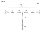
- FIG. 3 is an equivalent circuit diagram of a filter device to be compared;
- FIG. 5 is a graph showing transmission characteristics of the filter device according to Embodiment 1;
- 1 is a perspective view of a filter device according to Embodiment 1;
- FIG. 2 is an exploded plan view showing the configuration of the filter device according to Embodiment 1;
- FIG. 5 is a graph showing transmission characteristics with respect to frequency of the filter device according to Embodiment 1;
- FIG. 11 is a circuit diagram of a filter device according to Embodiment 4; FIG. 11 is an exploded plan view showing the configuration of a filter device according to Embodiment 5;
- FIG. 12 is an exploded plan view showing another configuration of the filter device according to Embodiment 5;
- a filter device, a high-frequency module, and a communication device according to the present embodiment will be described below.
- FIG. 1 is a circuit diagram of a filter device 100 according to Embodiment 1.
- the filter device 100 is, for example, a pass filter used in communication in a high frequency band such as several hundred MHz or several GHz.
- filter device 100 is an LC filter circuit, as shown in FIG.
- the filter device 100 includes a first terminal P1, a first inductor L1 connected to the first terminal P1, a second inductor L2 connected in series with the first inductor L1, and a second inductor L2. It includes a connected second terminal P2, a first connection point T1 between the first inductor L1 and the second inductor L2, and a capacitor Cg (first capacitor) connected between the ground.
- Filter device 100 also includes a capacitor C12 (third capacitor) connected in parallel with first inductor L1 and second inductor L2 between first terminal P1 and second terminal P2. Note that the first inductor L1 and the second inductor L2 are additively connected to each other. A summation connection leaves a negative inductor (-M) on the circuit configuration.
- the filter device 100 includes a capacitor C1 (second capacitor) connected between a second connection point T2 between the first terminal P1 and the first inductor L1 and the ground, and a capacitor C1 (second capacitor) connected between the second terminal P2 and the second inductor L1. It includes a third connection point T3 with L2 and a capacitor C2 (second capacitor) connected between the ground.
- the capacitors C1 and C2 are shunt capacitors. In filter device 100, both capacitor C1 and capacitor C2 are provided as shunt capacitors, but either capacitor C1 or capacitor C2 may be provided as a shunt capacitor.
- the filter device 100 increases the order (number of stages) of the filter by providing the shunt capacitor.
- a filter device it is known that in a general filter device that does not use a negative inductor, as the order (the number of stages) increases, the constant of each constituent element decreases.
- the first inductor L1 and the second inductor L2 required to obtain desired characteristics are magnetically coupled.
- the resulting negative inductor (-M) the sum of the first inductor L1 and the lossless inductor (+M), and the sum of the second inductor L2 and the lossless inductor (+M) are reduced in magnitude.
- FIG. 2 is an equivalent circuit diagram of the filter device 200 to be compared. Similar to the filter device 100, the filter device 200 has a first inductor L1 and a second inductor L2 connected in series between a first terminal P1 and a second terminal P2. Since the circuit shown in FIG. 2 is an equivalent circuit diagram of the filter device 200, a negative inductor ( ⁇ M) and a lossless inductor ( ⁇ M) generated by magnetic coupling between the first inductor L1 and the second inductor L2 +M) are also shown.
- ⁇ M negative inductor
- ⁇ M lossless inductor
- the filter device 100 can cancel the parasitic inductance of the capacitor Cg, and can reduce the constants of the constituent elements by providing the capacitors C1 and C2, which are shunt capacitors. Therefore, in the filter device 100, by reducing the inductances of the first inductor L1 and the second inductor L2, the parasitic resistance (equivalent series resistance (ESR)) itself can be reduced, and the insertion loss can be improved.
- ESR Equivalent series resistance
- FIG. 3 is a graph showing transmission characteristics of the filter device 100 according to the first embodiment.
- the horizontal axis is frequency and the vertical axis is insertion loss.
- the value of the coupling coefficient k should be large.
- the first inductor L1 and the second inductor L2 are approximately 0.31 nH
- the capacitor Cg is approximately 0.54 pF
- the capacitor C12 is approximately 0.31
- the coupling coefficient k is approximately 0.65.
- the values of the first inductor L1 and the second inductor L2 and the value of the coupling coefficient k are The transmission characteristics shown in FIG. 3 can be obtained.
- the first inductor L1 and the second inductor L2 about 0.38 nH
- the capacitor Cg about 0.30 pF
- the capacitor C12 about 0.24
- the coupling coefficient k about 0.35.
- the capacitors C1 and C2 newly provided in the filter device 100 are as small as about 0.16 pF, it is possible to obtain the transmission characteristics shown in FIG. 3 while keeping the size of the filter device 100 small.
- the filter device 100 is formed as one chip component by laminating a plurality of insulating layers on which electrodes such as coil patterns are formed by photolithography.
- the constant of each element can be reduced by providing the capacitors C1 and C2, which are shunt capacitors. Therefore, since the negative inductor (-M) and the lossless inductor (+M) required in the filter device 100 can also be reduced, the coupling coefficient k itself between the first inductor L1 and the second inductor L2 can also be reduced. can be done. Therefore, by providing the capacitors C1 and C2, which are shunt capacitors, the filter device 100 can secure the required coupling coefficient k while securing the necessary inductance value in the high frequency band.
- FIG. 4 is a perspective view of the filter device 100 according to Embodiment 1.
- FIG. FIG. 5 is an exploded plan view showing the configuration of the filter device 100 according to Embodiment 1.
- the filter device 100 is composed of an insulator 3 in which a plurality of insulating layers having wiring patterns of inductors and capacitors are laminated.
- the insulating layer is made of, for example, an insulating material containing borosilicate glass as a main component, a dielectric ceramic material such as a low-temperature fired ceramic, or an insulating resin such as a glass epoxy resin or a polyimide resin.
- the insulator 3 may not have clear interfaces between the insulating layers due to baking, hardening, or the like.
- the insulator 3 has a pair of main surfaces facing each other and side surfaces connecting the main surfaces. Wiring patterns of the first inductor L1, the second inductor L2, and the capacitors C1, C2, and Cg are formed on the main surface of the plurality of insulating layers forming the insulator 3 .
- the insulator 3 has a pair of main surfaces, the main surface of which is mounted on the substrate as the bottom surface, and the opposite main surface as the top surface. When viewed from one of the main surfaces (top surface), the four corners of the insulator 3 are provided with an electrode of the first terminal P1, an electrode of the second terminal P2, and electrodes of the ground terminals G1 and G2 to be grounded. is formed. Each electrode is formed on three surfaces of the insulator 3, namely, a side surface on the long side, a side surface on the short side, and a bottom surface.
- the filter device 100 the wiring pattern 16 (first wiring pattern) forming part of the first inductor L1 and the wiring pattern 12 (second wiring pattern) forming part of the second inductor L2 are arranged inside the insulator 3. are placed in Further, the filter device 100 has wiring patterns 11 and 13 (the wiring pattern 11 is grounded) forming a part of the capacitor Cg, a wiring pattern 15 forming a part of the capacitor C1 and the insulating layers 3d, 3g and 3j. Wiring patterns to be arranged (wiring pattern 15 is grounded), and wiring patterns 14 forming part of capacitor C2 and wiring patterns arranged on insulating layers 3b, 3e and 3h (wiring pattern 14 is grounded) are arranged inside the insulator 3 . It should be noted that the capacitor C12 is formed by the overlapping portion of the wiring pattern 16 and the wiring pattern 12. As shown in FIG. Moreover, the overlapping portion of the wiring pattern 16 and the wiring pattern 12 is strongly magnetically coupled.
- the wiring pattern 16 and the wiring pattern 12 are laminated in the direction between the main surfaces (the vertical direction in FIG. 4) inside the insulator 3 . Furthermore, the wiring pattern 16 and the wiring pattern 12 are alternately laminated within the insulator 3, and the first inductor L1 and the second inductor L2 are additively connected to each other. By laminating the wiring pattern 16 and the wiring pattern 12 in this manner, the required first inductor L1, second inductor L2, and coupling coefficient k are secured.
- the state in which the inductors are summatively connected means that when a current flows from one inductor to the other inductor through the connection point, the directions of the magnetic fields generated by the two inductors become the same and reinforce each other.
- It is a connected state that is, a connected state in which the magnetic flux interlinking with the wiring pattern forming the inductor is shared.
- the two inductors are coil-shaped and the openings of the coils overlap each other when viewed from above, the winding direction from the end of one coil to the connection point of the two coils and the winding direction from the connection point of the two coils The winding direction to the end of the other coil is the same.
- each layer of the filter device 100 will be described using the exploded plan view shown in FIG.
- the electrodes of the first terminal P1, the electrodes of the second terminal P2, the electrodes of the ground terminals G1 and G2, and the wiring patterns 11 to 16 are each formed on the insulating layers 3a to 3m by photolithography.
- An electrode of the first terminal P1, an electrode of the second terminal P2, and electrodes of the ground terminals G1 and G2 are formed at the four corners of the insulating layer 3a shown in FIG.
- the electrodes of the first terminals P1 formed in each layer are electrically connected by the electrodes formed on the side surfaces on the long side and the side surface on the short side shown in FIG.
- the electrode of the second terminal P2 and the electrodes of the ground terminals G1 and G2 formed on each layer are electrically connected to each other by the electrodes formed on the side surfaces on the long side and the side surfaces on the short side.
- the electrodes of the first terminal P1, the electrode of the second terminal P2, and the ground terminal G1 are formed on each layer by connecting the layers with via conductors.
- G2 may be electrically connected.
- the first terminal P1 and the second terminal P2 are arranged along one long side of the insulator 3, and the ground terminals G1 and G2 are arranged along the other long side of the insulator 3, as shown in FIG. arranged along the edges.
- the arrangement of the terminals is not limited to this, and in the filter device 100, the first terminal P1 and the second terminal P2 are arranged along one short side of the insulator 3, and the ground terminals G1 and G2 are arranged along one short side of the insulator 3. may be arranged along the other short side of the
- a wiring pattern 11 and a wiring pattern 12 are formed on the insulating layer 3b.
- the wiring pattern 11 is electrically connected to the electrodes of the ground terminals G1 and G2, and constitutes the ground-side electrode of the capacitor Cg.
- a portion of the wiring pattern 12 formed from the electrode of the second terminal P2 to the connection portion 12a along the long and short sides of the insulating layer 3b constitutes a part of the second inductor L2.
- a portion 12b of the wiring pattern 12 extending along the short side from the electrode of the second terminal P2 constitutes the electrode of the capacitor C2 on the third connection point T3 side.
- a wiring pattern 13, a wiring pattern 14 and a wiring pattern 15 are formed on the insulating layer 3c.
- the wiring pattern 13 is formed from the connecting portion 13a to the connecting portion 13b along the long side of the insulating layer 3c.
- the connecting portion 13a is electrically connected to the connecting portion 12a of the insulating layer 3b by a via conductor, and the connecting portion 13b is electrically connected to the connecting portion 16a of the insulating layer 3d by a via conductor.
- the wiring pattern 13 is also the first connection point T1 that connects the first inductor L1 and the second inductor L2, and forms a capacitor Cg with the wiring pattern 11 arranged on the insulating layer 3b or the like.
- the wiring pattern 14 is formed along the short side from the electrode of the ground terminal G2, and constitutes the ground-side electrode of the capacitor C2.
- the wiring pattern 15 is formed along the short side from the electrode of the ground terminal G1, and constitutes the ground-side electrode of the capacitor C1.
- a wiring pattern 11 and a wiring pattern 16 are formed on the insulating layer 3d.
- the wiring pattern 11 is electrically connected to the electrodes of the ground terminals G1 and G2, and constitutes the ground-side electrode of the capacitor Cg.
- a portion of the wiring pattern 16 formed from the electrode of the first terminal P1 to the connecting portion 16a along the long and short sides of the insulating layer 3d constitutes a part of the first inductor L1.
- a portion 16b of the wiring pattern 16 extending along the short side from the electrode of the first terminal P1 constitutes the electrode of the capacitor C1 on the second connection point T2 side.
- Subsequent layers are repetitions of the insulating layers 3b to 3d.
- the same wiring pattern as that of the insulating layer 3b is formed on the insulating layers 3e and 3h.
- the insulating layer 3f and the insulating layer 3i are formed with the same wiring pattern as that of the insulating layer 3c.
- the insulating layers 3g and 3j are formed with the same wiring pattern as that of the insulating layer 3d.
- the insulating layer 3k and the insulating layer 3l are formed only for the electrode of the first terminal P1, the electrode of the second terminal P2, and the electrodes of the ground terminals G1 and G2.
- the insulating layer 3m serves as an electrode of the first terminal P1, an electrode of the second terminal P2, and a ground for electrical connection with the wiring of the substrate. Electrodes of terminals G1 and G2 are formed at the four corners.
- the electrodes formed on the insulating layer 3m have a larger area than the other insulating layers 3a to 3l in order to be electrically connected to the wiring of the substrate.
- the filter device 100 laminates each of the plurality of insulating layers 3a to 3m shown in FIG. 5 and performs processing such as baking and curing.
- each of the wiring pattern 16 and the wiring pattern 12 has a loop shape of less than one turn when viewed from the top surface side. are combined to form a coil pattern with one or more turns. Therefore, in the filter device 100, the parallel-connected loop-shaped wiring patterns 16 and the wiring patterns 12 of less than one turn are alternately stacked to reduce the inductance values of the first inductor L1 and the second inductor L2 while reducing the high frequency. It reserves the necessary coupling coefficient k for use in bands.
- the wiring patterns 16 are formed on the insulating layers 3d, 3g, and 3j, and are electrically connected to each other by via conductors to be connected in parallel.
- the wiring patterns 12 are formed on the insulating layers 3b, 3e, and 3h, and are electrically connected to each other by via conductors to be connected in parallel.
- FIG. 6 is a graph showing transmission characteristics with respect to frequency of the filter device 100 according to the first embodiment.
- the horizontal axis is frequency and the vertical axis is loss.
- graph B is the simulation result of the return loss on the input side of the filter device 100 .
- Graph C is a simulation result of insertion loss in the filter device 100 .
- Graph D is a simulation result of reflection loss on the output side of the filter device 100 .
- the filter device 100 functions as a low-pass filter (LPF) with two attenuation poles around 13.5 GHz and 17.3 GHz as shown in FIG.
- LPF low-pass filter
- the filter device 100 As described above, in the filter device 100 according to the first embodiment, the first terminal P1, the first inductor L1 connected to the first terminal P1, and the second inductor L2 connected in series with the first inductor L1 , a second terminal P2 connected to the second inductor L2, a first connection point T1 between the first inductor L1 and the second inductor L2, and a capacitor Cg connected to the ground. Further, the filter device 100 is connected between a second connection point T2 between the first terminal P1 and the first inductor L1 and the ground, and between a third connection point T3 between the second terminal P2 and the second inductor L2 and the ground. and capacitors C1 and C2 connected to at least one of between and. The first inductor L1 and the second inductor L2 are additively connected to each other.
- the filter device 100 according to Embodiment 1 can secure the coupling coefficients necessary for use in a high frequency band, and can obtain a compact pass filter that can be used in a high frequency band.
- the filter device 100 can increase the number of elements that determine the resonance frequency, so that the constant of each element can be reduced, the degree of freedom in design can be improved, and the size of the device can be reduced.
- the first inductor L1, the second inductor L2, the capacitor Cg, and the capacitors C1 and C2 are formed in the insulator 3 having a pair of main surfaces facing each other and side surfaces connecting the main surfaces.
- the insulator 3 is arranged inside the insulator 3, and when viewed from above the plurality of wiring patterns 16 forming part of the first inductor L1 and one of the main surfaces (top surface), It is preferable to include a plurality of wiring patterns 12 arranged so as to at least partially overlap with the wiring pattern 16 and forming a part of the second inductor L2.
- the filter device 100 can realize a configuration of sum dynamic connection in which the directions of the currents flowing through the first inductor L1 and the second inductor L2 are the same, and the directions of the generated magnetic fields are also the same.
- the wiring pattern 16 and the wiring pattern 12 are preferably laminated in the direction between the main surfaces in the insulator 3 .
- the filter device 100 can arrange the wiring patterns of the first inductor L1 and the second inductor L2 so as to overlap each other, thereby strengthening the magnetic field coupling.
- the wiring patterns 16 and the wiring patterns 12 are preferably alternately laminated within the insulator 5 .
- the wiring patterns of the first inductor L1 and the second inductor L2 to be magnetically coupled can be arranged close to each other in the stacking direction, so that the magnetic coupling can be strengthened.
- the insulator 3 preferably includes an electrode connected to the first terminal P1, an electrode connected to the second terminal P2, and electrodes of the ground terminals G1 and G2. As a result, in the filter device 100, wiring patterns can be effectively arranged when the insulator 3 is viewed from above, and the size can be reduced.
- Each of the wiring pattern 16 and the wiring pattern 12 has a loop shape of less than one turn when viewed from one of the main surfaces (top surface), and the wiring pattern 16 is formed in the insulator 3. and the wiring pattern 12 are preferably combined to form a coil pattern having one or more turns.
- the filter device 100 can reduce the inductance values of the first inductor L1 and the second inductor L2 while ensuring the coupling coefficient k necessary for use in a high frequency band.
- the magnetic fluxes generated by the first inductor L1 and the second inductor L2 are strengthened while the inductors are connected to each other. can be formed. Thereby, the first inductor L1 and the second inductor L2 can be sum-connected.
- FIG. 7 is a circuit diagram of a filter device 100A according to the second embodiment.
- the same components as filter device 100 shown in FIG. 1 are denoted by the same reference numerals, and detailed description thereof will not be repeated.
- the filter device 100A includes a capacitor C1 (second capacitor) connected to the second connection point T2, and a third inductor L3 connected between the capacitor C1 and ground.
- the filter device 100A also includes a capacitor C2 (second capacitor) connected between the third connection point T3 and the ground.
- a third inductor L3 may be provided between the capacitor C2 and the ground in addition to between the capacitor C1 and the ground. Further, although the third inductor L3 is provided between the capacitor C2 and the ground, it may not be provided between the capacitor C1 and the ground.
- both the capacitor C1 and the capacitor C2 are provided with shunt capacitors.
- the filter device 100A provides a third inductor L3 between the provided shunt capacitor (capacitor C1 or capacitor C2) and the ground.
- FIG. 8 is a graph showing transmission characteristics with respect to frequency of the filter device according to the second embodiment.
- the parameters of the other elements are the same as the parameter values of the elements of the filter device 100 in the graph shown in FIG.
- the horizontal axis is the frequency
- the vertical axis is the insertion loss
- Graph F1 is a simulation result of insertion loss in a filter device without the third inductor L3.
- FIG. 9 is a graph showing another transmission characteristic with respect to frequency of the filter device according to the second embodiment.
- the horizontal axis is the frequency
- the vertical axis is the insertion loss
- Graph F1 is a simulation result of insertion loss in a filter device without the third inductor L3.
- the filter device 100A By providing the third inductor L3 connected in series with the shunt capacitor, the filter device 100A increases the number of attenuation poles as shown in FIGS. It is possible to improve the steepness between the attenuation bands.
- the filter device 100A further includes the third inductor L3 connected in series between the shunt capacitors (capacitors C1, C2) and the ground.
- the filter device 100A can form an attenuation pole in the attenuation band due to resonance between the shunt capacitors (capacitors C1 and C2) and the third inductor L3, thereby improving attenuation characteristics and steepness.
- shunt capacitors (capacitors C1 and C2) are provided for one unit including first inductor L1, second inductor L2, and capacitor Cg. explained.
- a configuration in which a plurality of units each including the first inductor L1, the second inductor L2, and the capacitor Cg are connected and a shunt capacitor is provided for each unit will be described.
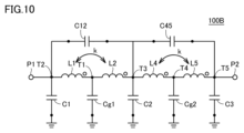
- FIG. 10 is a circuit diagram of a filter device 100B according to the third embodiment.
- filter device 100B shown in FIG. 10 the same configurations as filter device 100 shown in FIG. 1 are denoted by the same reference numerals, and detailed description thereof will not be repeated.
- the filter device 100B includes a first terminal P1, a first inductor L1 connected to the first terminal P1, a second inductor L2 connected in series with the first inductor L1, and a second inductor L2. It includes a fourth inductor L4 connected in series, a fifth inductor L5 connected in series with the fourth inductor L4, and a second terminal P2 connected to the fifth inductor L5.
- the filter device 100B includes a capacitor Cg1 (first capacitor) connected between a first connection point T1 between the first inductor L1 and the second inductor L2 and the ground, a fourth inductor L4 and a fifth inductor It includes a fourth connection point T4 with L5 and a capacitor Cg2 (first capacitor) connected between the ground.
- the first inductor L1 and the second inductor L2 are additively connected to each other, and the fourth inductor L4 and the fifth inductor L5 are additively connected to each other.
- the filter device 100B has a configuration in which a unit including the first inductor L1, the second inductor L2, and the capacitor Cg1 and a unit including the fourth inductor L4, the fifth inductor L5, and the capacitor Cg2 are connected. That is, the filter device 100B has a configuration in which two circuit units shown in the filter device 100 are connected in cascade. Further, filter device 100B is connected in parallel to capacitor C12 (third capacitor) connected in parallel to first inductor L1 and second inductor L2, and connected in parallel to fourth inductor L4 and fifth inductor L5. and a capacitor C45 (third capacitor).
- the filter device 100B the capacitor C1 (second capacitor) connected to the second connection point T2 as a shunt capacitor, the capacitor C2 (second capacitor) connected to the third connection point T3, and the fifth connection point T5 and a connected capacitor C3 (second capacitor).
- the filter device 100B is not limited to providing shunt capacitors at all of the second connection point T2, the third connection point T3, and the fifth connection point T5. and the fifth connection point T5, at least one of which may be provided with a shunt capacitor.
- the third inductor L3 described in the second embodiment may be connected in series between the shunt capacitors (capacitors C1, C2, C3) and the ground.
- FIG. 11 is a graph showing transmission characteristics with respect to frequency of the filter device according to Embodiment 3.
- the first inductor L1 and fourth inductor L4 approximately 0.325 nH
- the second inductor L2 and third inductor L3 approximately 0.326 nH
- capacitors Cg1 and Cg2 approximately 0.071 pF
- capacitors C12 and C45 approximately
- the filter device 100B is simulated with 0.171 pF
- capacitors C1 and C3 about 0.012 pF
- capacitor C2 about 0.371 pF
- coupling coefficient k 0.348.
- the horizontal axis is the frequency
- the vertical axis is the insertion loss
- the graph I1 is the simulation result of the insertion loss in the filter device 100B.
- Graph F1 is a simulation result of insertion loss in a filter device that does not include the fourth inductor L4 and the fifth inductor L5.
- the filter device 100B can improve the steepness of the attenuation band as shown in FIG. 11 by connecting a plurality of units including the first inductor L1, the second inductor L2, and the capacitor Cg as shown in FIG. can.
- each unit including the first inductor L1, the second inductor L2, and the capacitor Cg. can improve.
- FIG. 12 is a circuit diagram of a filter device 100C according to the fourth embodiment.
- the filter device 100C includes a first balanced terminal P1a, a first balanced inductor L1a connected to the first balanced terminal P1a, a second balanced inductor L2a connected in series with the first balanced inductor L1a, a second balanced terminal P2a connected to the second balanced inductor L2a. Furthermore, the filter device 100C includes a third balanced terminal P3a, a third balanced inductor L3a connected to the third balanced terminal P3a, a fourth balanced inductor L4a connected in series with the third balanced inductor L3a, and a fourth and a fourth balanced terminal P4a connected to the balanced inductor L4a.
- the filter device 100C is connected between a first connection point T1a between the first balanced inductor L1a and the second balanced inductor L2a and a second connection point T2a between the third balanced inductor L3a and the fourth balanced inductor L4a.
- a capacitor Cg first capacitor
- the filter device 100C is connected between a third connection point T3a between the first balanced terminal P1a and the first balanced inductor L1a and a fourth connection point T4a between the third balanced terminal P3a and the third balanced inductor L3a.
- the capacitors C1a and C2a are shunt capacitors. In the filter device 100C, both the capacitor C1a and the capacitor C2a are provided with shunt capacitors.
- the filter device 100C includes a capacitor C12a (third capacitor) connected in parallel to the first balanced inductor L1a and the second balanced inductor L2a between the first balanced terminal P1a and the second balanced terminal P2a. , and a capacitor C34a (third capacitor) connected in parallel to the third balanced inductor L3a and the fourth balanced inductor L4a between the third balanced terminal P3a and the fourth balanced terminal P4a.
- the first balanced inductor L1a and the second balanced inductor L2a are sum-connected to each other, and the third balanced inductor L3a and the fourth balanced inductor L4a are sum-connected to each other.
- a summation connection leaves a negative inductor (-M) on the circuit configuration.
- the first balanced inductor L1a and the second balanced inductor L2a are additively connected, and the third balanced inductor L3a and the fourth balanced inductor L4a are additively connected.
- a sum-and-connection configuration may also be used.
- the transmission characteristics of the filter device 100C according to Embodiment 4 can be the same as the transmission characteristics of the filter device 100 shown in FIG. 3 by adjusting the parameter values of each element.
- the first inductor L1, the second inductor L2, and the capacitors C1, C2, Cg, and C12 are formed inside the insulator 3 with the structure shown in FIGS. Ta.
- the capacitor Cg (first capacitor) has the wiring pattern 13 that connects the first inductor L1 and the second inductor L2 as one electrode, and the wiring pattern 11 that connects the ground terminals G1 and G2 as the other electrode.
- the structures of the first inductor L1, the second inductor L2, and the capacitor Cg are not limited to the structures shown in FIGS. A structure in which L2 and capacitor Cg are arranged in different regions may also be used.
- FIG. 13 is an exploded plan view showing the configuration of the filter device 100D according to Embodiment 1.
- the electrode of the first terminal P1, the electrode of the second terminal P2, the ground terminal G, the electrode of the non-connect terminal N, and the wiring patterns 21 to 25 are each formed on the insulating layers 3A to 3F by photolithography. be done.
- the insulating layer 3A shown in FIG. 13 has electrodes formed at the four corners. Specifically, the electrode of the first terminal P1 and the electrode of the second terminal P2 are arranged along one short side of the insulating layer 3A, and the electrode of the ground terminal G and the electrode of the non-connect terminal N are arranged along the insulating layer 3A. along the other short side of the
- the electrodes of the first terminals P1 formed in each layer are electrically connected by the electrodes formed on the side surfaces on the long side and the side surfaces on the short side.
- the electrodes of the second terminal P2, the ground terminal G and the non-connect terminal N formed on each layer are electrically connected to each other by the electrodes formed on the side surfaces of the long side and the short side.
- the electrodes of the first terminal P1, the electrode of the second terminal P2, and the ground terminal G are formed on each layer by connecting the layers with via conductors. and the electrode of the non-connect terminal N may be electrically connected.
- a wiring pattern 51, a wiring pattern 21, and a wiring pattern 61 are formed on the insulating layer 3B.
- the wiring pattern 51 is electrically connected to the electrode of the ground terminal G, and constitutes the electrode of the capacitor Cg (first capacitor) arranged on the left side of the insulating layer in the drawing.
- the wiring pattern 21 is a wiring for electrically connecting the wiring pattern 51 and the first inductor L1 disposed in the center of the drawing of the insulating layer, and is formed from the wiring pattern 51 to the connection portion 21a.
- the wiring pattern 61 is electrically connected to the electrode of the first terminal P1, and constitutes the electrode on the first terminal P1 side of the capacitor C12 (third capacitor) arranged on the right side of the insulating layer in the drawing.
- a wiring pattern 52, a wiring pattern 22, and a wiring pattern 62 are formed on the insulating layer 3C.
- the wiring pattern 52 is electrically connected to the electrode of the non-connect terminal N and constitutes the electrode of the capacitor Cg.
- the wiring pattern 22 constitutes a part of the first inductor L1, is formed from the connecting portion 22a to the connecting portion 22b, and forms a U-shaped pattern.
- Connection portion 22a is electrically connected to connection portion 21a of insulating layer 3B by a via conductor.
- a part of the wiring pattern 22 also functions as an electrode forming a capacitor C1 (second capacitor) with the ground wiring of the substrate.
- the wiring pattern 62 is electrically connected to the electrode of the second terminal P2 and constitutes the electrode of the capacitor C12 on the second terminal P2 side.
- a wiring pattern 53, a wiring pattern 23, and a wiring pattern 63 are formed on the insulating layer 3D.
- the wiring pattern 53 is electrically connected to the electrode of the ground terminal G and constitutes the electrode of the capacitor Cg.
- the wiring pattern 23 constitutes a part of the first inductor L1, is formed from the connecting portion 23a to the wiring pattern 63, and forms a rectangular pattern.
- the connecting portion 23a is electrically connected to the connecting portion 22b of the insulating layer 3C by a via conductor.
- the wiring pattern 63 is electrically connected to the electrode of the first terminal P1 and constitutes the electrode of the capacitor C12 on the first terminal P1 side.
- a wiring pattern 54, a wiring pattern 24, and a wiring pattern 64 are formed on the insulating layer 3E.
- the wiring pattern 54 is electrically connected to the electrode of the non-connect terminal N and constitutes the electrode of the capacitor Cg.
- the wiring pattern 24 constitutes a part of the second inductor L2, is formed from the connection part 24a to the wiring pattern 64, and forms a rectangular pattern.
- the connecting portion 24a is electrically connected to the connecting portion 23a of the insulating layer 3D by a via conductor.
- the wiring pattern 64 is electrically connected to the electrode of the second terminal P2 and constitutes the electrode of the capacitor C12 on the second terminal P2 side.
- a wiring pattern 55, a wiring pattern 25, a wiring pattern 26, and a wiring pattern 65 are formed on the insulating layer 3F.
- the wiring pattern 55 is electrically connected to the electrode of the ground terminal G and constitutes the electrode of the capacitor Cg.
- the wiring pattern 25 constitutes a part of the second inductor L2, is formed from the connecting portion 25a to the connecting portion 25b, and forms a U-shaped pattern.
- the connecting portion 25a is electrically connected to the connecting portion 24a of the insulating layer 3E by a via conductor.
- the wiring pattern 26 is wiring for electrically connecting the wiring pattern 55 and the second inductor L2, and is formed from the wiring pattern 55 to the connection portion 25b.
- the wiring pattern 65 is electrically connected to the electrode of the first terminal P1 and constitutes the electrode of the capacitor C12 on the first terminal P1 side.
- the filter device 100D laminates each of the plurality of insulating layers 3A to 3F shown in FIG. 13 and performs processing such as baking and curing.
- An electrode of the first terminal P1, an electrode of the second terminal P2, an electrode of the ground terminal G, and an electrode of the non-connect terminal N are formed on the side surface of the insulator 3 that has been subjected to a treatment such as baking or hardening.
- the first inductor L1, the second inductor L2, and the capacitor Cg are arranged in different regions inside the insulator 3. Therefore, the first inductor L1, the second inductor L2, and the capacitor Cg are arranged Wiring patterns 21 and 26 are provided for electrical connection.
- the first inductor L1 and the second inductor L2 are magnetically coupled to function as a transformer.
- the coupling coefficient k is approximately 0.53.
- the coupling coefficient k was obtained by simulating a configuration in which the outer diameter of the coil was 270 ⁇ m, the width of the wiring pattern was 30 ⁇ m, and the first inductor L1 and the second inductor L2 were each turned 1.5 times.
- the filter device 100D since the first inductor L1 and the second inductor L2 are connected via the capacitor Cg, parasitics such as the wiring patterns 51 to 55, the ground terminal G electrode, the non-connect terminal N electrode, etc.
- the inductance lowers the coupling coefficient k.
- the coupling coefficient k is approximately 0.32, which is approximately 0.2 lower than the configuration in which the first inductor L1 and the second inductor L2 are simply connected. are doing.
- FIG. 14 is an exploded plan view showing another configuration of the filter device according to Embodiment 5.
- the electrode of the first terminal P1, the electrode of the second terminal P2, the ground terminal G, the electrode of the non-connect terminal N, and the wiring patterns 21 to 25 are respectively connected to the insulating layers 3A to 3F. It is formed by photolithography.
- the insulating layer 3A shown in FIG. 14 has electrodes formed at the four corners.
- the same configurations as those of filter device 100D shown in FIG. 13 are denoted by the same reference numerals, and detailed description thereof will not be repeated.
- a wiring pattern 51, a wiring pattern 21, and a wiring pattern 61 are formed on the insulating layer 3B.
- the wiring pattern 21 has a connecting portion 21b formed between the wiring pattern 51 and the connecting portion 21a.
- a wiring pattern 52, a wiring pattern 22, and a wiring pattern 62 are formed on the insulating layer 3C. Further, a connection portion 22c is formed between the connection portion 22a and the wiring pattern 52. As shown in FIG. The connecting portion 22a is electrically connected to the connecting portion 21a of the insulating layer 3B by a via conductor, and the connecting portion 22c is electrically connected to the connecting portion 21b of the insulating layer 3B by a via conductor.
- a wiring pattern 53, a wiring pattern 23, and a wiring pattern 63 are formed on the insulating layer 3D. Further, a connecting portion 23b is formed between the wiring pattern 53 and the wiring pattern 23. As shown in FIG. The connecting portion 23a is electrically connected to the connecting portion 22b of the insulating layer 3C by a via conductor, and the connecting portion 23b is electrically connected to the connecting portion 23b of the insulating layer 3C by a via conductor.
- a wiring pattern 54, a wiring pattern 24, and a wiring pattern 64 are formed on the insulating layer 3E. Further, a connecting portion 24b is formed between the wiring pattern 54 and the wiring pattern 24. As shown in FIG. The connecting portion 24a is electrically connected to the connecting portion 23a of the insulating layer 3D by a via conductor, and the connecting portion 24b is electrically connected to the connecting portion 23b of the insulating layer 3D by a via conductor.
- a wiring pattern 55, a wiring pattern 25, a wiring pattern 27, and a wiring pattern 65 are formed on the insulating layer 3F. Further, a connecting portion 27a is formed between the wiring pattern 55 and the wiring pattern 25. As shown in FIG. The wiring pattern 27 is wiring for electrically connecting the connecting portion 27a and the connecting portion 25b.
- the connecting portion 25a is electrically connected to the connecting portion 24a of the insulating layer 3E by a via conductor, and the connecting portion 27a is electrically connected to the connecting portion 24b of the insulating layer 3E by a via conductor.
- the filter device 100E laminates each of the plurality of insulating layers 3A to 3F shown in FIG. 14 and performs processing such as baking and hardening.
- An electrode of the first terminal P1, an electrode of the second terminal P2, an electrode of the ground terminal G, and an electrode of the non-connect terminal N are formed on the side surface of the insulator 3 that has been subjected to a treatment such as baking or hardening.
- first inductor L1, second inductor L2, and capacitor Cg are arranged in different regions inside insulator 3, so first inductor L1, second inductor L2, and capacitor Cg are arranged in different regions.
- a wiring pattern 21 is provided for electrical connection.
- the wiring pattern 25 of the second inductor L2 is not directly connected to the capacitor Cg, but is connected to the wiring pattern 21 through via conductors. Therefore, in the filter device 100E, instead of connecting the first inductor L1 and the second inductor L2 via the capacitor Cg, the wiring pattern 21 connects the second inductor L2 to the first inductor L1 and then to the capacitor Cg. are doing.
- the filter device 100E parasitic inductances such as the wiring patterns 51 to 55, the electrodes of the ground terminal G, the electrodes of the non-connect terminal N, and the like do not occur, so that the reduction of the coupling coefficient k can be suppressed.
- the coupling coefficient k is approximately 0.41, which is approximately 0.1 lower than the configuration in which the first inductor L1 and the second inductor L2 are simply connected. can be reduced as much as possible. That is, the filter device 100E can improve the coupling coefficient k by about 10% compared to the filter device 100D.
- the filter devices 100D and 100E as shown in FIGS. 13 and 14, the first terminal P1 and the second terminal P2 are arranged along one short side of the insulator 3, and the ground terminal G1 and the non-connect terminal N are arranged. are arranged along the other short side of the insulator 3 .
- the arrangement of the terminals is not limited to this, and the filter devices 100D and 100E have the first terminal P1 and the second terminal P2 arranged along one long side of the insulator 3, the ground terminal G1 and the non-connect terminal N may be arranged along the other long side of insulator 3 . Further, in the filter devices 100D and 100E, the non-connect terminal N may be used as the ground terminal G.
- part of the wiring pattern 22 when the filter devices 100D and 100E are mounted on a substrate, part of the wiring pattern 22 also functions as an electrode forming a capacitor C1 (second capacitor) between the ground wiring of the substrate.
- capacitors C1 and C2 may be provided in the structures shown in filter devices 100D and 100E.
- 15 is an exploded plan view showing still another configuration of the filter device according to Embodiment 5.
- FIG. 15 the electrode of the first terminal P1, the electrode of the second terminal P2, the ground terminal G, the electrode of the non-connect terminal N, and the wiring patterns 21 to 25 are respectively connected to the insulating layers 3A to 3F. It is formed by photolithography.
- filter device 100F shown in FIG. 15 the same configurations as those of filter device 100D shown in FIG. 13 and filter device 100E shown in FIG. 14 are denoted by the same reference numerals, and detailed description thereof will not be repeated.
- a wiring pattern 52, a wiring pattern 22, and a wiring pattern 62 are formed on the insulating layer 3C.
- the wiring pattern 52 is electrically connected to the electrode of the ground terminal G and constitutes the electrode of the capacitor Cg (first capacitor) arranged on the left side of the insulating layer in the drawing. Further, the wiring pattern 52 is connected to a wiring pattern 52a functioning as one electrode of the capacitor C1 (second capacitor) and a wiring pattern 52b functioning as one electrode of the capacitor C2 (second capacitor).
- a wiring pattern 53, a wiring pattern 23, and a wiring pattern 63 are formed on the insulating layer 3D.
- the wiring pattern 23 constitutes a part of the first inductor L1, is formed from the connecting portion 23a to the wiring pattern 63, and forms a rectangular pattern. Furthermore, the wiring pattern 23 is connected to a wiring pattern 23c functioning as the other electrode of the capacitor C1.
- a wiring pattern 54, a wiring pattern 24, and a wiring pattern 64 are formed on the insulating layer 3E.
- the wiring pattern 24 constitutes a part of the second inductor L2, is formed from the connection part 24a to the wiring pattern 64, and forms a rectangular pattern. Furthermore, the wiring pattern 24 is connected to a wiring pattern 24c functioning as the other electrode of the capacitor C2.
- the filter device 100F laminates each of the plurality of insulating layers 3A to 3F shown in FIG. 15 and performs processing such as baking and hardening.
- An electrode of the first terminal P1, an electrode of the second terminal P2, an electrode of the ground terminal G, and an electrode of the non-connect terminal N are formed on the side surface of the insulator 3 that has been subjected to a treatment such as baking or hardening.
- the filter device 100E has electrodes (wiring pattern 23c and wiring pattern 52a, wiring pattern 24c and wiring pattern 52b) corresponding to the capacitors C1 and C2 (second capacitors) in the circuit diagram shown in FIG. Therefore, in filter device 100E, both capacitor C1 and capacitor C2 are provided as shunt capacitors.
- filter device 100E may have a configuration in which either capacitor C1 or capacitor C2 is provided as a shunt capacitor.
- the wiring pattern 23 formed on the insulating layer 3D is connected to the wiring pattern 63 forming the electrode of the capacitor C12, as shown in FIG.
- the wiring pattern 24 formed on the insulating layer 3E is connected to the wiring pattern 64 forming the electrode of the capacitor C12, as shown in FIG.
- the wiring pattern 23 and the wiring pattern 24 overlap when viewed from the top surface side, they can be regarded as part of the electrode of the capacitor C12. Therefore, by reducing the capacitance formed by the wiring patterns 63 and 64 by the capacitance formed by the wiring patterns 23 and 24, the areas of the wiring patterns 63 and 64 can be reduced. . That is, in filter device 100D, wiring pattern 63 and wiring pattern 64 for forming capacitor C12 can be made smaller. The effect is the same for filter devices 100E and 100F.
- the distance from the wiring pattern 63 to the electrode of the second terminal P2 formed on the insulating layer 3A is substantially the same. Therefore, in the filter device 100D, the parasitic inductance generated from the first terminal P1 to the second connection point T2 in the circuit diagram shown in FIG. 1 is substantially the same as the parasitic inductance generated from the second terminal P2 to the third connection point T3. , facilitating the design of the transformer coil. The effect is the same for filter devices 100E and 100F.
- FIG. 16 is a schematic diagram showing a communication device.
- the communication device 300 shown in FIG. 16 is capable of communication in bands including several 100 MHz and several GHz. Therefore, the communication device 300 is provided with a high-frequency module 150 that processes signals transmitted and received by the antenna, and the high-frequency module 150 is mounted on the substrate 310 .
- the communication device 300 is, for example, a mobile phone, smart phone, tablet, or the like.
- the high frequency module 150 includes electronic components such as the filter device 100, the switch 110 and the amplifier 120.
- the communication device 300 is provided with a power supply circuit 320 and the like in addition to the substrate 310 on which the high frequency module 150 is mounted.
- filter devices 100, 100A to 100C described so far have been described as (low-pass filters) LPFs, they can be similarly applied to band-stop filters (BSF).
- BSF band-stop filters
Landscapes
- Engineering & Computer Science (AREA)
- Power Engineering (AREA)
- Filters And Equalizers (AREA)
Priority Applications (3)
| Application Number | Priority Date | Filing Date | Title |
|---|---|---|---|
| CN202380015628.6A CN118476159A (zh) | 2022-02-09 | 2023-02-01 | 滤波器装置、高频模块以及通信装置 |
| JP2023580193A JP7670179B2 (ja) | 2022-02-09 | 2023-02-01 | フィルタ装置、高周波モジュール、および通信装置 |
| US18/746,111 US20240339982A1 (en) | 2022-02-09 | 2024-06-18 | Filter device, high-frequency module, and communication device |
Applications Claiming Priority (2)
| Application Number | Priority Date | Filing Date | Title |
|---|---|---|---|
| JP2022-018656 | 2022-02-09 | ||
| JP2022018656 | 2022-02-09 |
Related Child Applications (1)
| Application Number | Title | Priority Date | Filing Date |
|---|---|---|---|
| US18/746,111 Continuation US20240339982A1 (en) | 2022-02-09 | 2024-06-18 | Filter device, high-frequency module, and communication device |
Publications (1)
| Publication Number | Publication Date |
|---|---|
| WO2023153283A1 true WO2023153283A1 (ja) | 2023-08-17 |
Family
ID=87564324
Family Applications (1)
| Application Number | Title | Priority Date | Filing Date |
|---|---|---|---|
| PCT/JP2023/003160 Ceased WO2023153283A1 (ja) | 2022-02-09 | 2023-02-01 | フィルタ装置、高周波モジュール、および通信装置 |
Country Status (4)
| Country | Link |
|---|---|
| US (1) | US20240339982A1 (https=) |
| JP (1) | JP7670179B2 (https=) |
| CN (1) | CN118476159A (https=) |
| WO (1) | WO2023153283A1 (https=) |
Cited By (1)
| Publication number | Priority date | Publication date | Assignee | Title |
|---|---|---|---|---|
| WO2026079007A1 (ja) * | 2024-10-09 | 2026-04-16 | 株式会社村田製作所 | フィルタ回路 |
Families Citing this family (1)
| Publication number | Priority date | Publication date | Assignee | Title |
|---|---|---|---|---|
| CN113938107B (zh) * | 2021-11-15 | 2025-02-14 | 一巨自动化装备(上海)有限公司 | 一种dc端多级滤波结构、电机控制器及车辆 |
Citations (5)
| Publication number | Priority date | Publication date | Assignee | Title |
|---|---|---|---|---|
| CN1716684A (zh) * | 2004-06-29 | 2006-01-04 | 奇美通讯股份有限公司 | 多层陶瓷低通滤波器 |
| WO2011052374A1 (ja) * | 2009-11-02 | 2011-05-05 | エルメック株式会社 | コモンモードフィルタ |
| WO2017110179A1 (ja) * | 2015-12-24 | 2017-06-29 | 株式会社村田製作所 | 回路基板、フィルタ回路およびキャパシタンス素子 |
| WO2018025342A1 (ja) * | 2016-08-03 | 2018-02-08 | 三菱電機株式会社 | ノイズフィルタ回路 |
| JP2018064266A (ja) * | 2016-10-07 | 2018-04-19 | 株式会社村田製作所 | 高周波フィルタおよび高周波モジュール |
Family Cites Families (3)
| Publication number | Priority date | Publication date | Assignee | Title |
|---|---|---|---|---|
| JP5352881B2 (ja) * | 2009-09-25 | 2013-11-27 | 松江エルメック株式会社 | コモンモードフィルタ |
| JP6317890B2 (ja) * | 2013-05-17 | 2018-04-25 | 太陽誘電株式会社 | 高周波フィルタ及びこれを備える高周波モジュール |
| KR101900881B1 (ko) * | 2017-03-03 | 2018-09-21 | 주식회사 모다이노칩 | 적층형 소자 |
-
2023
- 2023-02-01 WO PCT/JP2023/003160 patent/WO2023153283A1/ja not_active Ceased
- 2023-02-01 JP JP2023580193A patent/JP7670179B2/ja active Active
- 2023-02-01 CN CN202380015628.6A patent/CN118476159A/zh active Pending
-
2024
- 2024-06-18 US US18/746,111 patent/US20240339982A1/en active Pending
Patent Citations (5)
| Publication number | Priority date | Publication date | Assignee | Title |
|---|---|---|---|---|
| CN1716684A (zh) * | 2004-06-29 | 2006-01-04 | 奇美通讯股份有限公司 | 多层陶瓷低通滤波器 |
| WO2011052374A1 (ja) * | 2009-11-02 | 2011-05-05 | エルメック株式会社 | コモンモードフィルタ |
| WO2017110179A1 (ja) * | 2015-12-24 | 2017-06-29 | 株式会社村田製作所 | 回路基板、フィルタ回路およびキャパシタンス素子 |
| WO2018025342A1 (ja) * | 2016-08-03 | 2018-02-08 | 三菱電機株式会社 | ノイズフィルタ回路 |
| JP2018064266A (ja) * | 2016-10-07 | 2018-04-19 | 株式会社村田製作所 | 高周波フィルタおよび高周波モジュール |
Cited By (1)
| Publication number | Priority date | Publication date | Assignee | Title |
|---|---|---|---|---|
| WO2026079007A1 (ja) * | 2024-10-09 | 2026-04-16 | 株式会社村田製作所 | フィルタ回路 |
Also Published As
| Publication number | Publication date |
|---|---|
| JPWO2023153283A1 (https=) | 2023-08-17 |
| JP7670179B2 (ja) | 2025-04-30 |
| CN118476159A (zh) | 2024-08-09 |
| US20240339982A1 (en) | 2024-10-10 |
Similar Documents
| Publication | Publication Date | Title |
|---|---|---|
| JP6635113B2 (ja) | 高周波モジュール | |
| JP6801826B2 (ja) | フィルタ素子 | |
| JP6074653B2 (ja) | コモンモードノイズフィルタ | |
| US9065506B2 (en) | High-frequency switch module | |
| US20240339982A1 (en) | Filter device, high-frequency module, and communication device | |
| JPWO2006134916A1 (ja) | 積層フィルタ | |
| CN105830343A (zh) | 滤波元器件 | |
| JP6760515B2 (ja) | 整合回路および通信装置 | |
| JP6183462B2 (ja) | 高周波モジュール | |
| JP5804076B2 (ja) | Lcフィルタ回路及び高周波モジュール | |
| JP2001210527A (ja) | 電子部品及び電子部品複合体 | |
| JPWO2011086822A1 (ja) | コモンモードフィルタおよびコモンモードフィルタ用インダクタ | |
| US10998876B2 (en) | Balun | |
| US11005443B2 (en) | Multilayer balun | |
| CN215896088U (zh) | 滤波器电路模块、滤波器电路元件、滤波器电路以及通信装置 | |
| CN208141948U (zh) | Lc复合器件 | |
| JP7021723B1 (ja) | コイルデバイス、回路素子モジュール及び電子機器 | |
| JPWO2016072403A1 (ja) | プリント基板へのフレキシブルケーブルの接続構造 | |
| CN116057649B (zh) | 滤波器模块以及电子设备 | |
| JP6471995B2 (ja) | コモンモードフィルタ | |
| JP7533592B2 (ja) | フィルタ、フィルタモジュール及び電子機器 | |
| JP2005244000A (ja) | バラントランス | |
| WO2023157577A1 (ja) | 電子部品 | |
| KR20260024633A (ko) | Srf를 갖는 수동 소자가 구현된 기판 또는 이를 포함하는 통신 모듈 | |
| CN101142741A (zh) | 滤波器 |
Legal Events
| Date | Code | Title | Description |
|---|---|---|---|
| 121 | Ep: the epo has been informed by wipo that ep was designated in this application |
Ref document number: 23752748 Country of ref document: EP Kind code of ref document: A1 |
|
| ENP | Entry into the national phase |
Ref document number: 2023580193 Country of ref document: JP Kind code of ref document: A |
|
| WWE | Wipo information: entry into national phase |
Ref document number: 202380015628.6 Country of ref document: CN |
|
| NENP | Non-entry into the national phase |
Ref country code: DE |
|
| 122 | Ep: pct application non-entry in european phase |
Ref document number: 23752748 Country of ref document: EP Kind code of ref document: A1 |