WO2023153283A1 - Filter device, high-frequency module, and communication device - Google Patents
Filter device, high-frequency module, and communication device Download PDFInfo
- Publication number
- WO2023153283A1 WO2023153283A1 PCT/JP2023/003160 JP2023003160W WO2023153283A1 WO 2023153283 A1 WO2023153283 A1 WO 2023153283A1 JP 2023003160 W JP2023003160 W JP 2023003160W WO 2023153283 A1 WO2023153283 A1 WO 2023153283A1
- Authority
- WO
- WIPO (PCT)
- Prior art keywords
- inductor
- filter device
- terminal
- wiring pattern
- capacitor
- Prior art date
Links
- 238000004891 communication Methods 0.000 title claims abstract description 18
- 239000003990 capacitor Substances 0.000 claims abstract description 198
- 239000012212 insulator Substances 0.000 claims description 49
- 239000004020 conductor Substances 0.000 claims description 20
- 230000008878 coupling Effects 0.000 description 27
- 238000010168 coupling process Methods 0.000 description 27
- 238000005859 coupling reaction Methods 0.000 description 27
- 230000005540 biological transmission Effects 0.000 description 17
- 238000010586 diagram Methods 0.000 description 15
- 238000003780 insertion Methods 0.000 description 13
- 230000037431 insertion Effects 0.000 description 13
- 238000004088 simulation Methods 0.000 description 12
- 239000000758 substrate Substances 0.000 description 10
- 230000003071 parasitic effect Effects 0.000 description 8
- 238000000206 photolithography Methods 0.000 description 5
- 238000012545 processing Methods 0.000 description 4
- 230000000694 effects Effects 0.000 description 3
- 238000004804 winding Methods 0.000 description 3
- 239000000470 constituent Substances 0.000 description 2
- 238000013461 design Methods 0.000 description 2
- 230000004907 flux Effects 0.000 description 2
- 238000010030 laminating Methods 0.000 description 2
- 230000004048 modification Effects 0.000 description 2
- 238000012986 modification Methods 0.000 description 2
- 239000005388 borosilicate glass Substances 0.000 description 1
- 239000000919 ceramic Substances 0.000 description 1
- 229910010293 ceramic material Inorganic materials 0.000 description 1
- 230000007423 decrease Effects 0.000 description 1
- 239000003822 epoxy resin Substances 0.000 description 1
- 239000011521 glass Substances 0.000 description 1
- 239000011810 insulating material Substances 0.000 description 1
- 239000000696 magnetic material Substances 0.000 description 1
- 238000000034 method Methods 0.000 description 1
- 229920000647 polyepoxide Polymers 0.000 description 1
- 229920001721 polyimide Polymers 0.000 description 1
- 239000009719 polyimide resin Substances 0.000 description 1
- 230000008569 process Effects 0.000 description 1
- 230000009467 reduction Effects 0.000 description 1
- 239000011347 resin Substances 0.000 description 1
- 229920005989 resin Polymers 0.000 description 1
- 102220298895 rs1025502215 Human genes 0.000 description 1
- 238000005728 strengthening Methods 0.000 description 1
Images


Classifications
-
- H—ELECTRICITY
- H01—ELECTRIC ELEMENTS
- H01F—MAGNETS; INDUCTANCES; TRANSFORMERS; SELECTION OF MATERIALS FOR THEIR MAGNETIC PROPERTIES
- H01F27/00—Details of transformers or inductances, in general
-
- H—ELECTRICITY
- H03—ELECTRONIC CIRCUITRY
- H03H—IMPEDANCE NETWORKS, e.g. RESONANT CIRCUITS; RESONATORS
- H03H7/00—Multiple-port networks comprising only passive electrical elements as network components
- H03H7/01—Frequency selective two-port networks
- H03H7/09—Filters comprising mutual inductance
Definitions
- the present disclosure relates to filter devices, high frequency modules, and communication devices.
- Patent Document 1 a low-pass filter described in Japanese Utility Model Publication No. 60-35297 (Patent Document 1) is known.
- the filter device has two inductors connected in series between an input terminal and an output terminal, the two inductors being magnetically coupled to each other.
- an object of the present disclosure is to provide a filter device that can be used in a high frequency band, a high frequency module including the same, and a communication device.
- a filter device includes a first terminal, a first inductor connected to the first terminal, a second inductor connected in series with the first inductor, and a second inductor connected to the second inductor. It has two terminals, a first connection point between the first inductor and the second inductor, and a first capacitor connected between the ground. Further, the filter device has at least one of between a second connection point between the first terminal and the first inductor and the ground and between a third connection point between the second terminal and the second inductor and the ground. and a second capacitor connected to the .
- the first inductor and the second inductor are additively connected to each other.
- a high-frequency module includes the filter device described above and an electronic component connected to the filter device. Further, a communication device according to an aspect of the present disclosure has the high frequency module.
- the second capacitor is connected to at least one of them, and the first inductor and the second inductor are additively connected to each other, a coupling coefficient necessary for use in a high frequency band can be ensured.
- FIG. 1 is a circuit diagram of a filter device according to Embodiment 1;
- FIG. 3 is an equivalent circuit diagram of a filter device to be compared;
- FIG. 5 is a graph showing transmission characteristics of the filter device according to Embodiment 1;
- 1 is a perspective view of a filter device according to Embodiment 1;
- FIG. 2 is an exploded plan view showing the configuration of the filter device according to Embodiment 1;
- FIG. 5 is a graph showing transmission characteristics with respect to frequency of the filter device according to Embodiment 1;
- FIG. 11 is a circuit diagram of a filter device according to Embodiment 4; FIG. 11 is an exploded plan view showing the configuration of a filter device according to Embodiment 5;
- FIG. 12 is an exploded plan view showing another configuration of the filter device according to Embodiment 5;
- a filter device, a high-frequency module, and a communication device according to the present embodiment will be described below.
- FIG. 1 is a circuit diagram of a filter device 100 according to Embodiment 1.
- the filter device 100 is, for example, a pass filter used in communication in a high frequency band such as several hundred MHz or several GHz.
- filter device 100 is an LC filter circuit, as shown in FIG.
- the filter device 100 includes a first terminal P1, a first inductor L1 connected to the first terminal P1, a second inductor L2 connected in series with the first inductor L1, and a second inductor L2. It includes a connected second terminal P2, a first connection point T1 between the first inductor L1 and the second inductor L2, and a capacitor Cg (first capacitor) connected between the ground.
- Filter device 100 also includes a capacitor C12 (third capacitor) connected in parallel with first inductor L1 and second inductor L2 between first terminal P1 and second terminal P2. Note that the first inductor L1 and the second inductor L2 are additively connected to each other. A summation connection leaves a negative inductor (-M) on the circuit configuration.
- the filter device 100 includes a capacitor C1 (second capacitor) connected between a second connection point T2 between the first terminal P1 and the first inductor L1 and the ground, and a capacitor C1 (second capacitor) connected between the second terminal P2 and the second inductor L1. It includes a third connection point T3 with L2 and a capacitor C2 (second capacitor) connected between the ground.
- the capacitors C1 and C2 are shunt capacitors. In filter device 100, both capacitor C1 and capacitor C2 are provided as shunt capacitors, but either capacitor C1 or capacitor C2 may be provided as a shunt capacitor.
- the filter device 100 increases the order (number of stages) of the filter by providing the shunt capacitor.
- a filter device it is known that in a general filter device that does not use a negative inductor, as the order (the number of stages) increases, the constant of each constituent element decreases.
- the first inductor L1 and the second inductor L2 required to obtain desired characteristics are magnetically coupled.
- the resulting negative inductor (-M) the sum of the first inductor L1 and the lossless inductor (+M), and the sum of the second inductor L2 and the lossless inductor (+M) are reduced in magnitude.
- FIG. 2 is an equivalent circuit diagram of the filter device 200 to be compared. Similar to the filter device 100, the filter device 200 has a first inductor L1 and a second inductor L2 connected in series between a first terminal P1 and a second terminal P2. Since the circuit shown in FIG. 2 is an equivalent circuit diagram of the filter device 200, a negative inductor ( ⁇ M) and a lossless inductor ( ⁇ M) generated by magnetic coupling between the first inductor L1 and the second inductor L2 +M) are also shown.
- ⁇ M negative inductor
- ⁇ M lossless inductor
- the filter device 100 can cancel the parasitic inductance of the capacitor Cg, and can reduce the constants of the constituent elements by providing the capacitors C1 and C2, which are shunt capacitors. Therefore, in the filter device 100, by reducing the inductances of the first inductor L1 and the second inductor L2, the parasitic resistance (equivalent series resistance (ESR)) itself can be reduced, and the insertion loss can be improved.
- ESR Equivalent series resistance
- FIG. 3 is a graph showing transmission characteristics of the filter device 100 according to the first embodiment.
- the horizontal axis is frequency and the vertical axis is insertion loss.
- the value of the coupling coefficient k should be large.
- the first inductor L1 and the second inductor L2 are approximately 0.31 nH
- the capacitor Cg is approximately 0.54 pF
- the capacitor C12 is approximately 0.31
- the coupling coefficient k is approximately 0.65.
- the values of the first inductor L1 and the second inductor L2 and the value of the coupling coefficient k are The transmission characteristics shown in FIG. 3 can be obtained.
- the first inductor L1 and the second inductor L2 about 0.38 nH
- the capacitor Cg about 0.30 pF
- the capacitor C12 about 0.24
- the coupling coefficient k about 0.35.
- the capacitors C1 and C2 newly provided in the filter device 100 are as small as about 0.16 pF, it is possible to obtain the transmission characteristics shown in FIG. 3 while keeping the size of the filter device 100 small.
- the filter device 100 is formed as one chip component by laminating a plurality of insulating layers on which electrodes such as coil patterns are formed by photolithography.
- the constant of each element can be reduced by providing the capacitors C1 and C2, which are shunt capacitors. Therefore, since the negative inductor (-M) and the lossless inductor (+M) required in the filter device 100 can also be reduced, the coupling coefficient k itself between the first inductor L1 and the second inductor L2 can also be reduced. can be done. Therefore, by providing the capacitors C1 and C2, which are shunt capacitors, the filter device 100 can secure the required coupling coefficient k while securing the necessary inductance value in the high frequency band.
- FIG. 4 is a perspective view of the filter device 100 according to Embodiment 1.
- FIG. FIG. 5 is an exploded plan view showing the configuration of the filter device 100 according to Embodiment 1.
- the filter device 100 is composed of an insulator 3 in which a plurality of insulating layers having wiring patterns of inductors and capacitors are laminated.
- the insulating layer is made of, for example, an insulating material containing borosilicate glass as a main component, a dielectric ceramic material such as a low-temperature fired ceramic, or an insulating resin such as a glass epoxy resin or a polyimide resin.
- the insulator 3 may not have clear interfaces between the insulating layers due to baking, hardening, or the like.
- the insulator 3 has a pair of main surfaces facing each other and side surfaces connecting the main surfaces. Wiring patterns of the first inductor L1, the second inductor L2, and the capacitors C1, C2, and Cg are formed on the main surface of the plurality of insulating layers forming the insulator 3 .
- the insulator 3 has a pair of main surfaces, the main surface of which is mounted on the substrate as the bottom surface, and the opposite main surface as the top surface. When viewed from one of the main surfaces (top surface), the four corners of the insulator 3 are provided with an electrode of the first terminal P1, an electrode of the second terminal P2, and electrodes of the ground terminals G1 and G2 to be grounded. is formed. Each electrode is formed on three surfaces of the insulator 3, namely, a side surface on the long side, a side surface on the short side, and a bottom surface.
- the filter device 100 the wiring pattern 16 (first wiring pattern) forming part of the first inductor L1 and the wiring pattern 12 (second wiring pattern) forming part of the second inductor L2 are arranged inside the insulator 3. are placed in Further, the filter device 100 has wiring patterns 11 and 13 (the wiring pattern 11 is grounded) forming a part of the capacitor Cg, a wiring pattern 15 forming a part of the capacitor C1 and the insulating layers 3d, 3g and 3j. Wiring patterns to be arranged (wiring pattern 15 is grounded), and wiring patterns 14 forming part of capacitor C2 and wiring patterns arranged on insulating layers 3b, 3e and 3h (wiring pattern 14 is grounded) are arranged inside the insulator 3 . It should be noted that the capacitor C12 is formed by the overlapping portion of the wiring pattern 16 and the wiring pattern 12. As shown in FIG. Moreover, the overlapping portion of the wiring pattern 16 and the wiring pattern 12 is strongly magnetically coupled.
- the wiring pattern 16 and the wiring pattern 12 are laminated in the direction between the main surfaces (the vertical direction in FIG. 4) inside the insulator 3 . Furthermore, the wiring pattern 16 and the wiring pattern 12 are alternately laminated within the insulator 3, and the first inductor L1 and the second inductor L2 are additively connected to each other. By laminating the wiring pattern 16 and the wiring pattern 12 in this manner, the required first inductor L1, second inductor L2, and coupling coefficient k are secured.
- the state in which the inductors are summatively connected means that when a current flows from one inductor to the other inductor through the connection point, the directions of the magnetic fields generated by the two inductors become the same and reinforce each other.
- It is a connected state that is, a connected state in which the magnetic flux interlinking with the wiring pattern forming the inductor is shared.
- the two inductors are coil-shaped and the openings of the coils overlap each other when viewed from above, the winding direction from the end of one coil to the connection point of the two coils and the winding direction from the connection point of the two coils The winding direction to the end of the other coil is the same.
- each layer of the filter device 100 will be described using the exploded plan view shown in FIG.
- the electrodes of the first terminal P1, the electrodes of the second terminal P2, the electrodes of the ground terminals G1 and G2, and the wiring patterns 11 to 16 are each formed on the insulating layers 3a to 3m by photolithography.
- An electrode of the first terminal P1, an electrode of the second terminal P2, and electrodes of the ground terminals G1 and G2 are formed at the four corners of the insulating layer 3a shown in FIG.
- the electrodes of the first terminals P1 formed in each layer are electrically connected by the electrodes formed on the side surfaces on the long side and the side surface on the short side shown in FIG.
- the electrode of the second terminal P2 and the electrodes of the ground terminals G1 and G2 formed on each layer are electrically connected to each other by the electrodes formed on the side surfaces on the long side and the side surfaces on the short side.
- the electrodes of the first terminal P1, the electrode of the second terminal P2, and the ground terminal G1 are formed on each layer by connecting the layers with via conductors.
- G2 may be electrically connected.
- the first terminal P1 and the second terminal P2 are arranged along one long side of the insulator 3, and the ground terminals G1 and G2 are arranged along the other long side of the insulator 3, as shown in FIG. arranged along the edges.
- the arrangement of the terminals is not limited to this, and in the filter device 100, the first terminal P1 and the second terminal P2 are arranged along one short side of the insulator 3, and the ground terminals G1 and G2 are arranged along one short side of the insulator 3. may be arranged along the other short side of the
- a wiring pattern 11 and a wiring pattern 12 are formed on the insulating layer 3b.
- the wiring pattern 11 is electrically connected to the electrodes of the ground terminals G1 and G2, and constitutes the ground-side electrode of the capacitor Cg.
- a portion of the wiring pattern 12 formed from the electrode of the second terminal P2 to the connection portion 12a along the long and short sides of the insulating layer 3b constitutes a part of the second inductor L2.
- a portion 12b of the wiring pattern 12 extending along the short side from the electrode of the second terminal P2 constitutes the electrode of the capacitor C2 on the third connection point T3 side.
- a wiring pattern 13, a wiring pattern 14 and a wiring pattern 15 are formed on the insulating layer 3c.
- the wiring pattern 13 is formed from the connecting portion 13a to the connecting portion 13b along the long side of the insulating layer 3c.
- the connecting portion 13a is electrically connected to the connecting portion 12a of the insulating layer 3b by a via conductor, and the connecting portion 13b is electrically connected to the connecting portion 16a of the insulating layer 3d by a via conductor.
- the wiring pattern 13 is also the first connection point T1 that connects the first inductor L1 and the second inductor L2, and forms a capacitor Cg with the wiring pattern 11 arranged on the insulating layer 3b or the like.
- the wiring pattern 14 is formed along the short side from the electrode of the ground terminal G2, and constitutes the ground-side electrode of the capacitor C2.
- the wiring pattern 15 is formed along the short side from the electrode of the ground terminal G1, and constitutes the ground-side electrode of the capacitor C1.
- a wiring pattern 11 and a wiring pattern 16 are formed on the insulating layer 3d.
- the wiring pattern 11 is electrically connected to the electrodes of the ground terminals G1 and G2, and constitutes the ground-side electrode of the capacitor Cg.
- a portion of the wiring pattern 16 formed from the electrode of the first terminal P1 to the connecting portion 16a along the long and short sides of the insulating layer 3d constitutes a part of the first inductor L1.
- a portion 16b of the wiring pattern 16 extending along the short side from the electrode of the first terminal P1 constitutes the electrode of the capacitor C1 on the second connection point T2 side.
- Subsequent layers are repetitions of the insulating layers 3b to 3d.
- the same wiring pattern as that of the insulating layer 3b is formed on the insulating layers 3e and 3h.
- the insulating layer 3f and the insulating layer 3i are formed with the same wiring pattern as that of the insulating layer 3c.
- the insulating layers 3g and 3j are formed with the same wiring pattern as that of the insulating layer 3d.
- the insulating layer 3k and the insulating layer 3l are formed only for the electrode of the first terminal P1, the electrode of the second terminal P2, and the electrodes of the ground terminals G1 and G2.
- the insulating layer 3m serves as an electrode of the first terminal P1, an electrode of the second terminal P2, and a ground for electrical connection with the wiring of the substrate. Electrodes of terminals G1 and G2 are formed at the four corners.
- the electrodes formed on the insulating layer 3m have a larger area than the other insulating layers 3a to 3l in order to be electrically connected to the wiring of the substrate.
- the filter device 100 laminates each of the plurality of insulating layers 3a to 3m shown in FIG. 5 and performs processing such as baking and curing.
- each of the wiring pattern 16 and the wiring pattern 12 has a loop shape of less than one turn when viewed from the top surface side. are combined to form a coil pattern with one or more turns. Therefore, in the filter device 100, the parallel-connected loop-shaped wiring patterns 16 and the wiring patterns 12 of less than one turn are alternately stacked to reduce the inductance values of the first inductor L1 and the second inductor L2 while reducing the high frequency. It reserves the necessary coupling coefficient k for use in bands.
- the wiring patterns 16 are formed on the insulating layers 3d, 3g, and 3j, and are electrically connected to each other by via conductors to be connected in parallel.
- the wiring patterns 12 are formed on the insulating layers 3b, 3e, and 3h, and are electrically connected to each other by via conductors to be connected in parallel.
- FIG. 6 is a graph showing transmission characteristics with respect to frequency of the filter device 100 according to the first embodiment.
- the horizontal axis is frequency and the vertical axis is loss.
- graph B is the simulation result of the return loss on the input side of the filter device 100 .
- Graph C is a simulation result of insertion loss in the filter device 100 .
- Graph D is a simulation result of reflection loss on the output side of the filter device 100 .
- the filter device 100 functions as a low-pass filter (LPF) with two attenuation poles around 13.5 GHz and 17.3 GHz as shown in FIG.
- LPF low-pass filter
- the filter device 100 As described above, in the filter device 100 according to the first embodiment, the first terminal P1, the first inductor L1 connected to the first terminal P1, and the second inductor L2 connected in series with the first inductor L1 , a second terminal P2 connected to the second inductor L2, a first connection point T1 between the first inductor L1 and the second inductor L2, and a capacitor Cg connected to the ground. Further, the filter device 100 is connected between a second connection point T2 between the first terminal P1 and the first inductor L1 and the ground, and between a third connection point T3 between the second terminal P2 and the second inductor L2 and the ground. and capacitors C1 and C2 connected to at least one of between and. The first inductor L1 and the second inductor L2 are additively connected to each other.
- the filter device 100 according to Embodiment 1 can secure the coupling coefficients necessary for use in a high frequency band, and can obtain a compact pass filter that can be used in a high frequency band.
- the filter device 100 can increase the number of elements that determine the resonance frequency, so that the constant of each element can be reduced, the degree of freedom in design can be improved, and the size of the device can be reduced.
- the first inductor L1, the second inductor L2, the capacitor Cg, and the capacitors C1 and C2 are formed in the insulator 3 having a pair of main surfaces facing each other and side surfaces connecting the main surfaces.
- the insulator 3 is arranged inside the insulator 3, and when viewed from above the plurality of wiring patterns 16 forming part of the first inductor L1 and one of the main surfaces (top surface), It is preferable to include a plurality of wiring patterns 12 arranged so as to at least partially overlap with the wiring pattern 16 and forming a part of the second inductor L2.
- the filter device 100 can realize a configuration of sum dynamic connection in which the directions of the currents flowing through the first inductor L1 and the second inductor L2 are the same, and the directions of the generated magnetic fields are also the same.
- the wiring pattern 16 and the wiring pattern 12 are preferably laminated in the direction between the main surfaces in the insulator 3 .
- the filter device 100 can arrange the wiring patterns of the first inductor L1 and the second inductor L2 so as to overlap each other, thereby strengthening the magnetic field coupling.
- the wiring patterns 16 and the wiring patterns 12 are preferably alternately laminated within the insulator 5 .
- the wiring patterns of the first inductor L1 and the second inductor L2 to be magnetically coupled can be arranged close to each other in the stacking direction, so that the magnetic coupling can be strengthened.
- the insulator 3 preferably includes an electrode connected to the first terminal P1, an electrode connected to the second terminal P2, and electrodes of the ground terminals G1 and G2. As a result, in the filter device 100, wiring patterns can be effectively arranged when the insulator 3 is viewed from above, and the size can be reduced.
- Each of the wiring pattern 16 and the wiring pattern 12 has a loop shape of less than one turn when viewed from one of the main surfaces (top surface), and the wiring pattern 16 is formed in the insulator 3. and the wiring pattern 12 are preferably combined to form a coil pattern having one or more turns.
- the filter device 100 can reduce the inductance values of the first inductor L1 and the second inductor L2 while ensuring the coupling coefficient k necessary for use in a high frequency band.
- the magnetic fluxes generated by the first inductor L1 and the second inductor L2 are strengthened while the inductors are connected to each other. can be formed. Thereby, the first inductor L1 and the second inductor L2 can be sum-connected.
- FIG. 7 is a circuit diagram of a filter device 100A according to the second embodiment.
- the same components as filter device 100 shown in FIG. 1 are denoted by the same reference numerals, and detailed description thereof will not be repeated.
- the filter device 100A includes a capacitor C1 (second capacitor) connected to the second connection point T2, and a third inductor L3 connected between the capacitor C1 and ground.
- the filter device 100A also includes a capacitor C2 (second capacitor) connected between the third connection point T3 and the ground.
- a third inductor L3 may be provided between the capacitor C2 and the ground in addition to between the capacitor C1 and the ground. Further, although the third inductor L3 is provided between the capacitor C2 and the ground, it may not be provided between the capacitor C1 and the ground.
- both the capacitor C1 and the capacitor C2 are provided with shunt capacitors.
- the filter device 100A provides a third inductor L3 between the provided shunt capacitor (capacitor C1 or capacitor C2) and the ground.
- FIG. 8 is a graph showing transmission characteristics with respect to frequency of the filter device according to the second embodiment.
- the parameters of the other elements are the same as the parameter values of the elements of the filter device 100 in the graph shown in FIG.
- the horizontal axis is the frequency
- the vertical axis is the insertion loss
- Graph F1 is a simulation result of insertion loss in a filter device without the third inductor L3.
- FIG. 9 is a graph showing another transmission characteristic with respect to frequency of the filter device according to the second embodiment.
- the horizontal axis is the frequency
- the vertical axis is the insertion loss
- Graph F1 is a simulation result of insertion loss in a filter device without the third inductor L3.
- the filter device 100A By providing the third inductor L3 connected in series with the shunt capacitor, the filter device 100A increases the number of attenuation poles as shown in FIGS. It is possible to improve the steepness between the attenuation bands.
- the filter device 100A further includes the third inductor L3 connected in series between the shunt capacitors (capacitors C1, C2) and the ground.
- the filter device 100A can form an attenuation pole in the attenuation band due to resonance between the shunt capacitors (capacitors C1 and C2) and the third inductor L3, thereby improving attenuation characteristics and steepness.
- shunt capacitors (capacitors C1 and C2) are provided for one unit including first inductor L1, second inductor L2, and capacitor Cg. explained.
- a configuration in which a plurality of units each including the first inductor L1, the second inductor L2, and the capacitor Cg are connected and a shunt capacitor is provided for each unit will be described.
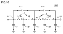
- FIG. 10 is a circuit diagram of a filter device 100B according to the third embodiment.
- filter device 100B shown in FIG. 10 the same configurations as filter device 100 shown in FIG. 1 are denoted by the same reference numerals, and detailed description thereof will not be repeated.
- the filter device 100B includes a first terminal P1, a first inductor L1 connected to the first terminal P1, a second inductor L2 connected in series with the first inductor L1, and a second inductor L2. It includes a fourth inductor L4 connected in series, a fifth inductor L5 connected in series with the fourth inductor L4, and a second terminal P2 connected to the fifth inductor L5.
- the filter device 100B includes a capacitor Cg1 (first capacitor) connected between a first connection point T1 between the first inductor L1 and the second inductor L2 and the ground, a fourth inductor L4 and a fifth inductor It includes a fourth connection point T4 with L5 and a capacitor Cg2 (first capacitor) connected between the ground.
- the first inductor L1 and the second inductor L2 are additively connected to each other, and the fourth inductor L4 and the fifth inductor L5 are additively connected to each other.
- the filter device 100B has a configuration in which a unit including the first inductor L1, the second inductor L2, and the capacitor Cg1 and a unit including the fourth inductor L4, the fifth inductor L5, and the capacitor Cg2 are connected. That is, the filter device 100B has a configuration in which two circuit units shown in the filter device 100 are connected in cascade. Further, filter device 100B is connected in parallel to capacitor C12 (third capacitor) connected in parallel to first inductor L1 and second inductor L2, and connected in parallel to fourth inductor L4 and fifth inductor L5. and a capacitor C45 (third capacitor).
- the filter device 100B the capacitor C1 (second capacitor) connected to the second connection point T2 as a shunt capacitor, the capacitor C2 (second capacitor) connected to the third connection point T3, and the fifth connection point T5 and a connected capacitor C3 (second capacitor).
- the filter device 100B is not limited to providing shunt capacitors at all of the second connection point T2, the third connection point T3, and the fifth connection point T5. and the fifth connection point T5, at least one of which may be provided with a shunt capacitor.
- the third inductor L3 described in the second embodiment may be connected in series between the shunt capacitors (capacitors C1, C2, C3) and the ground.
- FIG. 11 is a graph showing transmission characteristics with respect to frequency of the filter device according to Embodiment 3.
- the first inductor L1 and fourth inductor L4 approximately 0.325 nH
- the second inductor L2 and third inductor L3 approximately 0.326 nH
- capacitors Cg1 and Cg2 approximately 0.071 pF
- capacitors C12 and C45 approximately
- the filter device 100B is simulated with 0.171 pF
- capacitors C1 and C3 about 0.012 pF
- capacitor C2 about 0.371 pF
- coupling coefficient k 0.348.
- the horizontal axis is the frequency
- the vertical axis is the insertion loss
- the graph I1 is the simulation result of the insertion loss in the filter device 100B.
- Graph F1 is a simulation result of insertion loss in a filter device that does not include the fourth inductor L4 and the fifth inductor L5.
- the filter device 100B can improve the steepness of the attenuation band as shown in FIG. 11 by connecting a plurality of units including the first inductor L1, the second inductor L2, and the capacitor Cg as shown in FIG. can.
- each unit including the first inductor L1, the second inductor L2, and the capacitor Cg. can improve.
- FIG. 12 is a circuit diagram of a filter device 100C according to the fourth embodiment.
- the filter device 100C includes a first balanced terminal P1a, a first balanced inductor L1a connected to the first balanced terminal P1a, a second balanced inductor L2a connected in series with the first balanced inductor L1a, a second balanced terminal P2a connected to the second balanced inductor L2a. Furthermore, the filter device 100C includes a third balanced terminal P3a, a third balanced inductor L3a connected to the third balanced terminal P3a, a fourth balanced inductor L4a connected in series with the third balanced inductor L3a, and a fourth and a fourth balanced terminal P4a connected to the balanced inductor L4a.
- the filter device 100C is connected between a first connection point T1a between the first balanced inductor L1a and the second balanced inductor L2a and a second connection point T2a between the third balanced inductor L3a and the fourth balanced inductor L4a.
- a capacitor Cg first capacitor
- the filter device 100C is connected between a third connection point T3a between the first balanced terminal P1a and the first balanced inductor L1a and a fourth connection point T4a between the third balanced terminal P3a and the third balanced inductor L3a.
- the capacitors C1a and C2a are shunt capacitors. In the filter device 100C, both the capacitor C1a and the capacitor C2a are provided with shunt capacitors.
- the filter device 100C includes a capacitor C12a (third capacitor) connected in parallel to the first balanced inductor L1a and the second balanced inductor L2a between the first balanced terminal P1a and the second balanced terminal P2a. , and a capacitor C34a (third capacitor) connected in parallel to the third balanced inductor L3a and the fourth balanced inductor L4a between the third balanced terminal P3a and the fourth balanced terminal P4a.
- the first balanced inductor L1a and the second balanced inductor L2a are sum-connected to each other, and the third balanced inductor L3a and the fourth balanced inductor L4a are sum-connected to each other.
- a summation connection leaves a negative inductor (-M) on the circuit configuration.
- the first balanced inductor L1a and the second balanced inductor L2a are additively connected, and the third balanced inductor L3a and the fourth balanced inductor L4a are additively connected.
- a sum-and-connection configuration may also be used.
- the transmission characteristics of the filter device 100C according to Embodiment 4 can be the same as the transmission characteristics of the filter device 100 shown in FIG. 3 by adjusting the parameter values of each element.
- the first inductor L1, the second inductor L2, and the capacitors C1, C2, Cg, and C12 are formed inside the insulator 3 with the structure shown in FIGS. Ta.
- the capacitor Cg (first capacitor) has the wiring pattern 13 that connects the first inductor L1 and the second inductor L2 as one electrode, and the wiring pattern 11 that connects the ground terminals G1 and G2 as the other electrode.
- the structures of the first inductor L1, the second inductor L2, and the capacitor Cg are not limited to the structures shown in FIGS. A structure in which L2 and capacitor Cg are arranged in different regions may also be used.
- FIG. 13 is an exploded plan view showing the configuration of the filter device 100D according to Embodiment 1.
- the electrode of the first terminal P1, the electrode of the second terminal P2, the ground terminal G, the electrode of the non-connect terminal N, and the wiring patterns 21 to 25 are each formed on the insulating layers 3A to 3F by photolithography. be done.
- the insulating layer 3A shown in FIG. 13 has electrodes formed at the four corners. Specifically, the electrode of the first terminal P1 and the electrode of the second terminal P2 are arranged along one short side of the insulating layer 3A, and the electrode of the ground terminal G and the electrode of the non-connect terminal N are arranged along the insulating layer 3A. along the other short side of the
- the electrodes of the first terminals P1 formed in each layer are electrically connected by the electrodes formed on the side surfaces on the long side and the side surfaces on the short side.
- the electrodes of the second terminal P2, the ground terminal G and the non-connect terminal N formed on each layer are electrically connected to each other by the electrodes formed on the side surfaces of the long side and the short side.
- the electrodes of the first terminal P1, the electrode of the second terminal P2, and the ground terminal G are formed on each layer by connecting the layers with via conductors. and the electrode of the non-connect terminal N may be electrically connected.
- a wiring pattern 51, a wiring pattern 21, and a wiring pattern 61 are formed on the insulating layer 3B.
- the wiring pattern 51 is electrically connected to the electrode of the ground terminal G, and constitutes the electrode of the capacitor Cg (first capacitor) arranged on the left side of the insulating layer in the drawing.
- the wiring pattern 21 is a wiring for electrically connecting the wiring pattern 51 and the first inductor L1 disposed in the center of the drawing of the insulating layer, and is formed from the wiring pattern 51 to the connection portion 21a.
- the wiring pattern 61 is electrically connected to the electrode of the first terminal P1, and constitutes the electrode on the first terminal P1 side of the capacitor C12 (third capacitor) arranged on the right side of the insulating layer in the drawing.
- a wiring pattern 52, a wiring pattern 22, and a wiring pattern 62 are formed on the insulating layer 3C.
- the wiring pattern 52 is electrically connected to the electrode of the non-connect terminal N and constitutes the electrode of the capacitor Cg.
- the wiring pattern 22 constitutes a part of the first inductor L1, is formed from the connecting portion 22a to the connecting portion 22b, and forms a U-shaped pattern.
- Connection portion 22a is electrically connected to connection portion 21a of insulating layer 3B by a via conductor.
- a part of the wiring pattern 22 also functions as an electrode forming a capacitor C1 (second capacitor) with the ground wiring of the substrate.
- the wiring pattern 62 is electrically connected to the electrode of the second terminal P2 and constitutes the electrode of the capacitor C12 on the second terminal P2 side.
- a wiring pattern 53, a wiring pattern 23, and a wiring pattern 63 are formed on the insulating layer 3D.
- the wiring pattern 53 is electrically connected to the electrode of the ground terminal G and constitutes the electrode of the capacitor Cg.
- the wiring pattern 23 constitutes a part of the first inductor L1, is formed from the connecting portion 23a to the wiring pattern 63, and forms a rectangular pattern.
- the connecting portion 23a is electrically connected to the connecting portion 22b of the insulating layer 3C by a via conductor.
- the wiring pattern 63 is electrically connected to the electrode of the first terminal P1 and constitutes the electrode of the capacitor C12 on the first terminal P1 side.
- a wiring pattern 54, a wiring pattern 24, and a wiring pattern 64 are formed on the insulating layer 3E.
- the wiring pattern 54 is electrically connected to the electrode of the non-connect terminal N and constitutes the electrode of the capacitor Cg.
- the wiring pattern 24 constitutes a part of the second inductor L2, is formed from the connection part 24a to the wiring pattern 64, and forms a rectangular pattern.
- the connecting portion 24a is electrically connected to the connecting portion 23a of the insulating layer 3D by a via conductor.
- the wiring pattern 64 is electrically connected to the electrode of the second terminal P2 and constitutes the electrode of the capacitor C12 on the second terminal P2 side.
- a wiring pattern 55, a wiring pattern 25, a wiring pattern 26, and a wiring pattern 65 are formed on the insulating layer 3F.
- the wiring pattern 55 is electrically connected to the electrode of the ground terminal G and constitutes the electrode of the capacitor Cg.
- the wiring pattern 25 constitutes a part of the second inductor L2, is formed from the connecting portion 25a to the connecting portion 25b, and forms a U-shaped pattern.
- the connecting portion 25a is electrically connected to the connecting portion 24a of the insulating layer 3E by a via conductor.
- the wiring pattern 26 is wiring for electrically connecting the wiring pattern 55 and the second inductor L2, and is formed from the wiring pattern 55 to the connection portion 25b.
- the wiring pattern 65 is electrically connected to the electrode of the first terminal P1 and constitutes the electrode of the capacitor C12 on the first terminal P1 side.
- the filter device 100D laminates each of the plurality of insulating layers 3A to 3F shown in FIG. 13 and performs processing such as baking and curing.
- An electrode of the first terminal P1, an electrode of the second terminal P2, an electrode of the ground terminal G, and an electrode of the non-connect terminal N are formed on the side surface of the insulator 3 that has been subjected to a treatment such as baking or hardening.
- the first inductor L1, the second inductor L2, and the capacitor Cg are arranged in different regions inside the insulator 3. Therefore, the first inductor L1, the second inductor L2, and the capacitor Cg are arranged Wiring patterns 21 and 26 are provided for electrical connection.
- the first inductor L1 and the second inductor L2 are magnetically coupled to function as a transformer.
- the coupling coefficient k is approximately 0.53.
- the coupling coefficient k was obtained by simulating a configuration in which the outer diameter of the coil was 270 ⁇ m, the width of the wiring pattern was 30 ⁇ m, and the first inductor L1 and the second inductor L2 were each turned 1.5 times.
- the filter device 100D since the first inductor L1 and the second inductor L2 are connected via the capacitor Cg, parasitics such as the wiring patterns 51 to 55, the ground terminal G electrode, the non-connect terminal N electrode, etc.
- the inductance lowers the coupling coefficient k.
- the coupling coefficient k is approximately 0.32, which is approximately 0.2 lower than the configuration in which the first inductor L1 and the second inductor L2 are simply connected. are doing.
- FIG. 14 is an exploded plan view showing another configuration of the filter device according to Embodiment 5.
- the electrode of the first terminal P1, the electrode of the second terminal P2, the ground terminal G, the electrode of the non-connect terminal N, and the wiring patterns 21 to 25 are respectively connected to the insulating layers 3A to 3F. It is formed by photolithography.
- the insulating layer 3A shown in FIG. 14 has electrodes formed at the four corners.
- the same configurations as those of filter device 100D shown in FIG. 13 are denoted by the same reference numerals, and detailed description thereof will not be repeated.
- a wiring pattern 51, a wiring pattern 21, and a wiring pattern 61 are formed on the insulating layer 3B.
- the wiring pattern 21 has a connecting portion 21b formed between the wiring pattern 51 and the connecting portion 21a.
- a wiring pattern 52, a wiring pattern 22, and a wiring pattern 62 are formed on the insulating layer 3C. Further, a connection portion 22c is formed between the connection portion 22a and the wiring pattern 52. As shown in FIG. The connecting portion 22a is electrically connected to the connecting portion 21a of the insulating layer 3B by a via conductor, and the connecting portion 22c is electrically connected to the connecting portion 21b of the insulating layer 3B by a via conductor.
- a wiring pattern 53, a wiring pattern 23, and a wiring pattern 63 are formed on the insulating layer 3D. Further, a connecting portion 23b is formed between the wiring pattern 53 and the wiring pattern 23. As shown in FIG. The connecting portion 23a is electrically connected to the connecting portion 22b of the insulating layer 3C by a via conductor, and the connecting portion 23b is electrically connected to the connecting portion 23b of the insulating layer 3C by a via conductor.
- a wiring pattern 54, a wiring pattern 24, and a wiring pattern 64 are formed on the insulating layer 3E. Further, a connecting portion 24b is formed between the wiring pattern 54 and the wiring pattern 24. As shown in FIG. The connecting portion 24a is electrically connected to the connecting portion 23a of the insulating layer 3D by a via conductor, and the connecting portion 24b is electrically connected to the connecting portion 23b of the insulating layer 3D by a via conductor.
- a wiring pattern 55, a wiring pattern 25, a wiring pattern 27, and a wiring pattern 65 are formed on the insulating layer 3F. Further, a connecting portion 27a is formed between the wiring pattern 55 and the wiring pattern 25. As shown in FIG. The wiring pattern 27 is wiring for electrically connecting the connecting portion 27a and the connecting portion 25b.
- the connecting portion 25a is electrically connected to the connecting portion 24a of the insulating layer 3E by a via conductor, and the connecting portion 27a is electrically connected to the connecting portion 24b of the insulating layer 3E by a via conductor.
- the filter device 100E laminates each of the plurality of insulating layers 3A to 3F shown in FIG. 14 and performs processing such as baking and hardening.
- An electrode of the first terminal P1, an electrode of the second terminal P2, an electrode of the ground terminal G, and an electrode of the non-connect terminal N are formed on the side surface of the insulator 3 that has been subjected to a treatment such as baking or hardening.
- first inductor L1, second inductor L2, and capacitor Cg are arranged in different regions inside insulator 3, so first inductor L1, second inductor L2, and capacitor Cg are arranged in different regions.
- a wiring pattern 21 is provided for electrical connection.
- the wiring pattern 25 of the second inductor L2 is not directly connected to the capacitor Cg, but is connected to the wiring pattern 21 through via conductors. Therefore, in the filter device 100E, instead of connecting the first inductor L1 and the second inductor L2 via the capacitor Cg, the wiring pattern 21 connects the second inductor L2 to the first inductor L1 and then to the capacitor Cg. are doing.
- the filter device 100E parasitic inductances such as the wiring patterns 51 to 55, the electrodes of the ground terminal G, the electrodes of the non-connect terminal N, and the like do not occur, so that the reduction of the coupling coefficient k can be suppressed.
- the coupling coefficient k is approximately 0.41, which is approximately 0.1 lower than the configuration in which the first inductor L1 and the second inductor L2 are simply connected. can be reduced as much as possible. That is, the filter device 100E can improve the coupling coefficient k by about 10% compared to the filter device 100D.
- the filter devices 100D and 100E as shown in FIGS. 13 and 14, the first terminal P1 and the second terminal P2 are arranged along one short side of the insulator 3, and the ground terminal G1 and the non-connect terminal N are arranged. are arranged along the other short side of the insulator 3 .
- the arrangement of the terminals is not limited to this, and the filter devices 100D and 100E have the first terminal P1 and the second terminal P2 arranged along one long side of the insulator 3, the ground terminal G1 and the non-connect terminal N may be arranged along the other long side of insulator 3 . Further, in the filter devices 100D and 100E, the non-connect terminal N may be used as the ground terminal G.
- part of the wiring pattern 22 when the filter devices 100D and 100E are mounted on a substrate, part of the wiring pattern 22 also functions as an electrode forming a capacitor C1 (second capacitor) between the ground wiring of the substrate.
- capacitors C1 and C2 may be provided in the structures shown in filter devices 100D and 100E.
- 15 is an exploded plan view showing still another configuration of the filter device according to Embodiment 5.
- FIG. 15 the electrode of the first terminal P1, the electrode of the second terminal P2, the ground terminal G, the electrode of the non-connect terminal N, and the wiring patterns 21 to 25 are respectively connected to the insulating layers 3A to 3F. It is formed by photolithography.
- filter device 100F shown in FIG. 15 the same configurations as those of filter device 100D shown in FIG. 13 and filter device 100E shown in FIG. 14 are denoted by the same reference numerals, and detailed description thereof will not be repeated.
- a wiring pattern 52, a wiring pattern 22, and a wiring pattern 62 are formed on the insulating layer 3C.
- the wiring pattern 52 is electrically connected to the electrode of the ground terminal G and constitutes the electrode of the capacitor Cg (first capacitor) arranged on the left side of the insulating layer in the drawing. Further, the wiring pattern 52 is connected to a wiring pattern 52a functioning as one electrode of the capacitor C1 (second capacitor) and a wiring pattern 52b functioning as one electrode of the capacitor C2 (second capacitor).
- a wiring pattern 53, a wiring pattern 23, and a wiring pattern 63 are formed on the insulating layer 3D.
- the wiring pattern 23 constitutes a part of the first inductor L1, is formed from the connecting portion 23a to the wiring pattern 63, and forms a rectangular pattern. Furthermore, the wiring pattern 23 is connected to a wiring pattern 23c functioning as the other electrode of the capacitor C1.
- a wiring pattern 54, a wiring pattern 24, and a wiring pattern 64 are formed on the insulating layer 3E.
- the wiring pattern 24 constitutes a part of the second inductor L2, is formed from the connection part 24a to the wiring pattern 64, and forms a rectangular pattern. Furthermore, the wiring pattern 24 is connected to a wiring pattern 24c functioning as the other electrode of the capacitor C2.
- the filter device 100F laminates each of the plurality of insulating layers 3A to 3F shown in FIG. 15 and performs processing such as baking and hardening.
- An electrode of the first terminal P1, an electrode of the second terminal P2, an electrode of the ground terminal G, and an electrode of the non-connect terminal N are formed on the side surface of the insulator 3 that has been subjected to a treatment such as baking or hardening.
- the filter device 100E has electrodes (wiring pattern 23c and wiring pattern 52a, wiring pattern 24c and wiring pattern 52b) corresponding to the capacitors C1 and C2 (second capacitors) in the circuit diagram shown in FIG. Therefore, in filter device 100E, both capacitor C1 and capacitor C2 are provided as shunt capacitors.
- filter device 100E may have a configuration in which either capacitor C1 or capacitor C2 is provided as a shunt capacitor.
- the wiring pattern 23 formed on the insulating layer 3D is connected to the wiring pattern 63 forming the electrode of the capacitor C12, as shown in FIG.
- the wiring pattern 24 formed on the insulating layer 3E is connected to the wiring pattern 64 forming the electrode of the capacitor C12, as shown in FIG.
- the wiring pattern 23 and the wiring pattern 24 overlap when viewed from the top surface side, they can be regarded as part of the electrode of the capacitor C12. Therefore, by reducing the capacitance formed by the wiring patterns 63 and 64 by the capacitance formed by the wiring patterns 23 and 24, the areas of the wiring patterns 63 and 64 can be reduced. . That is, in filter device 100D, wiring pattern 63 and wiring pattern 64 for forming capacitor C12 can be made smaller. The effect is the same for filter devices 100E and 100F.
- the distance from the wiring pattern 63 to the electrode of the second terminal P2 formed on the insulating layer 3A is substantially the same. Therefore, in the filter device 100D, the parasitic inductance generated from the first terminal P1 to the second connection point T2 in the circuit diagram shown in FIG. 1 is substantially the same as the parasitic inductance generated from the second terminal P2 to the third connection point T3. , facilitating the design of the transformer coil. The effect is the same for filter devices 100E and 100F.
- FIG. 16 is a schematic diagram showing a communication device.
- the communication device 300 shown in FIG. 16 is capable of communication in bands including several 100 MHz and several GHz. Therefore, the communication device 300 is provided with a high-frequency module 150 that processes signals transmitted and received by the antenna, and the high-frequency module 150 is mounted on the substrate 310 .
- the communication device 300 is, for example, a mobile phone, smart phone, tablet, or the like.
- the high frequency module 150 includes electronic components such as the filter device 100, the switch 110 and the amplifier 120.
- the communication device 300 is provided with a power supply circuit 320 and the like in addition to the substrate 310 on which the high frequency module 150 is mounted.
- filter devices 100, 100A to 100C described so far have been described as (low-pass filters) LPFs, they can be similarly applied to band-stop filters (BSF).
- BSF band-stop filters
Landscapes
- Engineering & Computer Science (AREA)
- Power Engineering (AREA)
- Filters And Equalizers (AREA)
Abstract
The present disclosure provides a filter device that can be used in a high-frequency band, a high-frequency module including the same, and a communication device. A filter device (100) according to the present disclosure comprises a first terminal (P1), a first inductor (L1), a second inductor (L2), a second terminal (P2), and a capacitor (Cg) connected between a first connection point (T1) and the ground. Further, the filter device (100) includes capacitors (C1, C2) connected to at least one of between a second connection point (T2) between the first terminal (P1) and the first inductor (L1) and the ground, or between a third connection point (T3) between the second terminal (P2) and the second inductor (L2) and the ground. The first inductor (L1) and the second inductor (L2) are additively connected to each other.
Description
本開示は、フィルタ装置、高周波モジュール、および通信装置に関する。
The present disclosure relates to filter devices, high frequency modules, and communication devices.
フィルタ装置として、実公昭60-35297号公報(特許文献1)に記載のローパスフィルタが知られている。当該フィルタ装置は、入力端子と出力端子との間に直列に接続された2つのインダクタを有し、この2つのインダクタが互いに磁界結合している。
As a filter device, a low-pass filter described in Japanese Utility Model Publication No. 60-35297 (Patent Document 1) is known. The filter device has two inductors connected in series between an input terminal and an output terminal, the two inductors being magnetically coupled to each other.
特許文献1に記載のフィルタ装置では、所望の特性を得るためにインダクタ間の磁界結合を大きくする必要がある。しかし、当該フィルタ装置では、フィルタ回路として設計に必要なインダクタンスの値を確保しつつ、そのインダクタ間で強い磁界結合を発生させることは難しかった。
In the filter device described in Patent Document 1, it is necessary to increase the magnetic field coupling between inductors in order to obtain desired characteristics. However, in the filter device, it is difficult to generate a strong magnetic field coupling between the inductors while securing an inductance value necessary for designing the filter circuit.
特に、数100MHzや数GHzなどの高周波帯の通信でフィルタ装置を使用する場合、損失の大きい磁性体を使用することができず、寄生インダクタンス(等価直列インダクタンス(ESL:Equivalent Series Inductance))が漏れインダクタンスとして機能するなどして必要な結合係数を確保することが困難であった。
In particular, when using a filter device for communication in a high frequency band such as several 100 MHz or several GHz, it is not possible to use magnetic materials with large losses, and parasitic inductance (equivalent series inductance (ESL)) leaks. It was difficult to ensure the necessary coupling coefficient by functioning as an inductance.
そこで、本開示の目的は、高周波帯で使用することができるフィルタ装置、それを含む高周波モジュール、および通信装置を提供することである。
Therefore, an object of the present disclosure is to provide a filter device that can be used in a high frequency band, a high frequency module including the same, and a communication device.
本開示の一形態に係るフィルタ装置は、第1端子と、第1端子と接続される第1インダクタと、第1インダクタと直列に接続される第2インダクタと、第2インダクタと接続される第2端子と、第1インダクタと第2インダクタとの第1接続点と、グランドとの間に接続される第1キャパシタと、を備える。さらに、フィルタ装置は、第1端子と第1インダクタとの第2接続点と、グランドとの間、および第2端子と第2インダクタとの第3接続点と、グランドとの間のうち少なくとも一方に接続される第2キャパシタと、を備える。第1インダクタと第2インダクタとは、互いに和動接続される。
A filter device according to an aspect of the present disclosure includes a first terminal, a first inductor connected to the first terminal, a second inductor connected in series with the first inductor, and a second inductor connected to the second inductor. It has two terminals, a first connection point between the first inductor and the second inductor, and a first capacitor connected between the ground. Further, the filter device has at least one of between a second connection point between the first terminal and the first inductor and the ground and between a third connection point between the second terminal and the second inductor and the ground. and a second capacitor connected to the . The first inductor and the second inductor are additively connected to each other.
本開示の一形態に係る高周波モジュールは、上記のフィルタ装置と、フィルタ装置と接続する電子部品と、を含む。また、本開示の一形態に係る通信装置は、当該高周波モジュールを有する。
A high-frequency module according to one aspect of the present disclosure includes the filter device described above and an electronic component connected to the filter device. Further, a communication device according to an aspect of the present disclosure has the high frequency module.
本開示の一形態によれば、第1端子と第1インダクタとの第2接続点と、グランドとの間、および第2端子と第2インダクタとの第3接続点と、グランドとの間のうち少なくとも一方に接続される第2キャパシタを備え、第1インダクタと第2インダクタとは、互いに和動接続されるので、高周波帯で使用するために必要な結合係数を確保することができる。
According to one aspect of the present disclosure, between the second connection point between the first terminal and the first inductor and the ground, and between the third connection point between the second terminal and the second inductor and the ground Since the second capacitor is connected to at least one of them, and the first inductor and the second inductor are additively connected to each other, a coupling coefficient necessary for use in a high frequency band can be ensured.
以下に、本実施の形態に係るフィルタ装置、高周波モジュール、および通信装置について説明する。
A filter device, a high-frequency module, and a communication device according to the present embodiment will be described below.
(実施の形態1)
まず、実施の形態1に係るフィルタ装置について図面を参照しながら説明する。図1は、実施の形態1に係るフィルタ装置100の回路図である。フィルタ装置100は、例えば、数100MHzや数GHzなど高周波帯の通信で使用するパスフィルタである。特に、フィルタ装置100は、図1に示すように、LCフィルタ回路である。 (Embodiment 1)
First, a filter device according toEmbodiment 1 will be described with reference to the drawings. FIG. 1 is a circuit diagram of a filter device 100 according to Embodiment 1. FIG. The filter device 100 is, for example, a pass filter used in communication in a high frequency band such as several hundred MHz or several GHz. In particular, filter device 100 is an LC filter circuit, as shown in FIG.
まず、実施の形態1に係るフィルタ装置について図面を参照しながら説明する。図1は、実施の形態1に係るフィルタ装置100の回路図である。フィルタ装置100は、例えば、数100MHzや数GHzなど高周波帯の通信で使用するパスフィルタである。特に、フィルタ装置100は、図1に示すように、LCフィルタ回路である。 (Embodiment 1)
First, a filter device according to
具体的に、フィルタ装置100は、第1端子P1と、第1端子P1と接続される第1インダクタL1と、第1インダクタL1と直列に接続される第2インダクタL2と、第2インダクタL2と接続される第2端子P2と、第1インダクタL1と第2インダクタL2との第1接続点T1と、グランドとの間に接続されるキャパシタCg(第1キャパシタ)と、を含む。また、フィルタ装置100は、第1端子P1と第2端子P2との間に、第1インダクタL1および第2インダクタL2に対して並列に接続されるキャパシタC12(第3キャパシタ)を含む。なお、第1インダクタL1と第2インダクタL2とは、互いに和動接続される。和動接続により、回路構成上に負のインダクタ(-M)を残している。
Specifically, the filter device 100 includes a first terminal P1, a first inductor L1 connected to the first terminal P1, a second inductor L2 connected in series with the first inductor L1, and a second inductor L2. It includes a connected second terminal P2, a first connection point T1 between the first inductor L1 and the second inductor L2, and a capacitor Cg (first capacitor) connected between the ground. Filter device 100 also includes a capacitor C12 (third capacitor) connected in parallel with first inductor L1 and second inductor L2 between first terminal P1 and second terminal P2. Note that the first inductor L1 and the second inductor L2 are additively connected to each other. A summation connection leaves a negative inductor (-M) on the circuit configuration.
さらに、フィルタ装置100は、第1端子P1と第1インダクタL1との第2接続点T2と、グランドとの間に接続されるキャパシタC1(第2キャパシタ)と、第2端子P2と第2インダクタL2との第3接続点T3と、グランドとの間に接続されるキャパシタC2(第2キャパシタ)と、を含む。このキャパシタC1,C2は、シャントキャパシタである。フィルタ装置100では、シャントキャパシタとしてキャパシタC1とキャパシタC2との両方を設けているが、シャントキャパシタとしてキャパシタC1またはキャパシタC2のいずれか一方を設ける構成でもよい。
Further, the filter device 100 includes a capacitor C1 (second capacitor) connected between a second connection point T2 between the first terminal P1 and the first inductor L1 and the ground, and a capacitor C1 (second capacitor) connected between the second terminal P2 and the second inductor L1. It includes a third connection point T3 with L2 and a capacitor C2 (second capacitor) connected between the ground. The capacitors C1 and C2 are shunt capacitors. In filter device 100, both capacitor C1 and capacitor C2 are provided as shunt capacitors, but either capacitor C1 or capacitor C2 may be provided as a shunt capacitor.
フィルタ装置100は、シャントキャパシタを設けることでフィルタの次数(段数)が増える。フィルタ装置では、負のインダクタを用いていない一般的なフィルタ装置においては次数(段数)が増えるに従い、構成する各素子の定数が小さくなることが知られている。負のインダクタを用いたフィルタ装置の場合には知られていないが、シャントキャパシタを設けることで、所望の特性を得るために必要な第1インダクタL1と第2インダクタL2とが磁気結合することで生じる負のインダクタ(-M)、第1インダクタL1と無損失インダクタ(+M)との和、および第2インダクタL2と無損失インダクタ(+M)との和の大きさが小さくなることを見出した。
The filter device 100 increases the order (number of stages) of the filter by providing the shunt capacitor. In a filter device, it is known that in a general filter device that does not use a negative inductor, as the order (the number of stages) increases, the constant of each constituent element decreases. Although not known in the case of a filter device using a negative inductor, by providing a shunt capacitor, the first inductor L1 and the second inductor L2 required to obtain desired characteristics are magnetically coupled. We have found that the resulting negative inductor (-M), the sum of the first inductor L1 and the lossless inductor (+M), and the sum of the second inductor L2 and the lossless inductor (+M) are reduced in magnitude.
ここで、シャントキャパシタであるキャパシタC1,C2を設けない比較対象であるフィルタ装置について説明する。図2は、比較対象であるフィルタ装置200の等価回路図である。フィルタ装置200は、フィルタ装置100と同様に、第1端子P1と第2端子P2との間に、第1インダクタL1と第2インダクタL2とが直列に接続されている。なお、図2に示す回路は、フィルタ装置200の等価回路図であるので、第1インダクタL1と第2インダクタL2とが磁気結合することで生じる負のインダクタ(-M)、および無損失インダクタ(+M)も図示している。
Here, a comparison filter device in which the capacitors C1 and C2, which are shunt capacitors, are not provided will be described. FIG. 2 is an equivalent circuit diagram of the filter device 200 to be compared. Similar to the filter device 100, the filter device 200 has a first inductor L1 and a second inductor L2 connected in series between a first terminal P1 and a second terminal P2. Since the circuit shown in FIG. 2 is an equivalent circuit diagram of the filter device 200, a negative inductor (−M) and a lossless inductor (−M) generated by magnetic coupling between the first inductor L1 and the second inductor L2 +M) are also shown.
フィルタ装置100は、フィルタ装置200と同様に、キャパシタCgの寄生インダクタンスを打ち消すことができるとともに、シャントキャパシタであるキャパシタC1,C2を設けることで構成する各素子の定数を小さくすることができる。そのため、フィルタ装置100では、第1インダクタL1および第2インダクタL2のインダクタンスを小さくすることで寄生抵抗(等価直列抵抗(ESR))自体を小さくでき挿入損失(Insertion Loss)を改善することができる。
As with the filter device 200, the filter device 100 can cancel the parasitic inductance of the capacitor Cg, and can reduce the constants of the constituent elements by providing the capacitors C1 and C2, which are shunt capacitors. Therefore, in the filter device 100, by reducing the inductances of the first inductor L1 and the second inductor L2, the parasitic resistance (equivalent series resistance (ESR)) itself can be reduced, and the insertion loss can be improved.
さらに、フィルタ装置100は、第1インダクタL1と第2インダクタL2とが磁気結合することで生じる無損失インダクタ(+M)により寄生抵抗を小さくでき挿入損失を改善することができる。図3は、実施の形態1に係るフィルタ装置100の伝送特性を示すグラフである。図3において、横軸は周波数、縦軸は挿入損失である。
Furthermore, the filter device 100 can reduce the parasitic resistance and improve the insertion loss by the lossless inductor (+M) generated by magnetically coupling the first inductor L1 and the second inductor L2. FIG. 3 is a graph showing transmission characteristics of the filter device 100 according to the first embodiment. In FIG. 3, the horizontal axis is frequency and the vertical axis is insertion loss.
ここで、フィルタ装置100の比較対象であるフィルタ装置200において、図3に示す伝送特性と同等の特性を得るためには、フィルタ装置200の第1インダクタL1および第2インダクタL2の値は小さく、結合係数kの値は大きくする必要がある。具体的に、フィルタ装置200では、第1インダクタL1および第2インダクタL2=約0.31nH、キャパシタCg=約0.54pF、キャパシタC12=約0.31、結合係数k=約0.65とする必要がある。しかし、フィルタ装置200を現実に作る場合、第1インダクタL1および第2インダクタL2の値が小さいため、必要な結合係数kの値を得ることが困難であった。
Here, in filter device 200 to which filter device 100 is compared, in order to obtain characteristics equivalent to the transmission characteristics shown in FIG. The value of the coupling coefficient k should be large. Specifically, in the filter device 200, the first inductor L1 and the second inductor L2 are approximately 0.31 nH, the capacitor Cg is approximately 0.54 pF, the capacitor C12 is approximately 0.31, and the coupling coefficient k is approximately 0.65. There is a need. However, when actually making the filter device 200, it was difficult to obtain the necessary value of the coupling coefficient k because the values of the first inductor L1 and the second inductor L2 were small.
一方、本実施の形態に係るフィルタ装置100では、シャントキャパシタであるキャパシタC1,C2を設けることで、現実に作ることができる第1インダクタL1および第2インダクタL2の値、結合係数kの値で図3に示す伝送特性を得ることができる。具体的に、フィルタ装置100では、第1インダクタL1および第2インダクタL2=約0.38nH、キャパシタCg=約0.30pF、キャパシタC12=約0.24、結合係数k=約0.35である。なお、フィルタ装置100において新たに設けたキャパシタC1,C2=約0.16pFと小さいので、フィルタ装置100自体を小型化したまま、図3に示す伝送特性を得ることが可能となっている。
On the other hand, in the filter device 100 according to the present embodiment, by providing the capacitors C1 and C2, which are shunt capacitors, the values of the first inductor L1 and the second inductor L2 and the value of the coupling coefficient k are The transmission characteristics shown in FIG. 3 can be obtained. Specifically, in the filter device 100, the first inductor L1 and the second inductor L2=about 0.38 nH, the capacitor Cg=about 0.30 pF, the capacitor C12=about 0.24, and the coupling coefficient k=about 0.35. . Since the capacitors C1 and C2 newly provided in the filter device 100 are as small as about 0.16 pF, it is possible to obtain the transmission characteristics shown in FIG. 3 while keeping the size of the filter device 100 small.
また、フィルタ装置100は、後述するように、フォトリソ工法でコイルパターンなどの電極を形成した絶縁層を複数積層して1つのチップ部品として形成している。
As will be described later, the filter device 100 is formed as one chip component by laminating a plurality of insulating layers on which electrodes such as coil patterns are formed by photolithography.
前述したように、フィルタ装置100では、シャントキャパシタであるキャパシタC1,C2を設けることで各素子の定数を小さくすることができる。そのため、フィルタ装置100において必要となる負のインダクタ(-M)および無損失インダクタ(+M)も小さくすることができるので、第1インダクタL1と第2インダクタL2との結合係数k自体も小さくすることができる。したがって、フィルタ装置100は、シャントキャパシタであるキャパシタC1,C2を設けることで、高周波帯において必要なインダクタンスの値を確保しつつ、必要となる結合係数kを確保することが可能となる。
As described above, in the filter device 100, the constant of each element can be reduced by providing the capacitors C1 and C2, which are shunt capacitors. Therefore, since the negative inductor (-M) and the lossless inductor (+M) required in the filter device 100 can also be reduced, the coupling coefficient k itself between the first inductor L1 and the second inductor L2 can also be reduced. can be done. Therefore, by providing the capacitors C1 and C2, which are shunt capacitors, the filter device 100 can secure the required coupling coefficient k while securing the necessary inductance value in the high frequency band.
次に、フィルタ装置100の構造について説明する。図4は、実施の形態1に係るフィルタ装置100の斜視図である。図5は、実施の形態1に係るフィルタ装置100の構成を示す分解平面図である。フィルタ装置100は、図4および図5に示すようにインダクタやキャパシタの配線パターンを形成した絶縁層が複数枚積層された絶縁体3で構成されている。なお、絶縁層は、例えば、硼珪酸ガラスを主成分とする絶縁材料や、低温焼成セラミックなどの誘電体セラミック材料、ガラスエポキシ樹脂、ポリイミド樹脂等の絶縁樹脂などの材料からなる。また、絶縁体3は、焼成や硬化等の処理によって、複数の絶縁層の界面が明確となっていない場合がある。
Next, the structure of the filter device 100 will be described. FIG. 4 is a perspective view of the filter device 100 according to Embodiment 1. FIG. FIG. 5 is an exploded plan view showing the configuration of the filter device 100 according to Embodiment 1. FIG. As shown in FIGS. 4 and 5, the filter device 100 is composed of an insulator 3 in which a plurality of insulating layers having wiring patterns of inductors and capacitors are laminated. The insulating layer is made of, for example, an insulating material containing borosilicate glass as a main component, a dielectric ceramic material such as a low-temperature fired ceramic, or an insulating resin such as a glass epoxy resin or a polyimide resin. Moreover, the insulator 3 may not have clear interfaces between the insulating layers due to baking, hardening, or the like.
絶縁体3は、互いに対向する1対の主面と主面間を結ぶ側面とを有している。絶縁体3を構成する複数の絶縁層の主面上に、第1インダクタL1、第2インダクタL2、およびキャパシタC1,C2,Cgの配線パターンが形成されている。なお、絶縁体3は、1対の主面のうち基板に実装する側の主面を底面、反対側の主面を天面とする。主面のうち一方の面(天面)側から平面視した場合に、絶縁体3の四隅には、第1端子P1の電極、第2端子P2の電極、接地するグランド端子G1,G2の電極が形成されている。各々の電極は、絶縁体3の長辺側の側面、短辺側の側面、および底面側の3面に形成されている。
The insulator 3 has a pair of main surfaces facing each other and side surfaces connecting the main surfaces. Wiring patterns of the first inductor L1, the second inductor L2, and the capacitors C1, C2, and Cg are formed on the main surface of the plurality of insulating layers forming the insulator 3 . The insulator 3 has a pair of main surfaces, the main surface of which is mounted on the substrate as the bottom surface, and the opposite main surface as the top surface. When viewed from one of the main surfaces (top surface), the four corners of the insulator 3 are provided with an electrode of the first terminal P1, an electrode of the second terminal P2, and electrodes of the ground terminals G1 and G2 to be grounded. is formed. Each electrode is formed on three surfaces of the insulator 3, namely, a side surface on the long side, a side surface on the short side, and a bottom surface.
フィルタ装置100は、第1インダクタL1の一部を構成する配線パターン16(第1配線パターン)、第2インダクタL2の一部を構成する配線パターン12(第2配線パターン)が絶縁体3の内部に配置されている。さらに、フィルタ装置100は、キャパシタCgの一部を構成する配線パターン11,13(配線パターン11は接地される)、キャパシタC1の一部を構成する配線パターン15と絶縁層3d,3g,3jに配置される配線パターン(配線パターン15は接地される)、およびキャパシタC2の一部を構成する配線パターン14と絶縁層3b,3e,3hに配置される配線パターン(配線パターン14は接地される)が絶縁体3の内部に配置されている。なお、キャパシタC12は、配線パターン16と配線パターン12との重なり部分で構成される。また、配線パターン16と配線パターン12との重なり部分において、強く磁界結合している。
In the filter device 100, the wiring pattern 16 (first wiring pattern) forming part of the first inductor L1 and the wiring pattern 12 (second wiring pattern) forming part of the second inductor L2 are arranged inside the insulator 3. are placed in Further, the filter device 100 has wiring patterns 11 and 13 (the wiring pattern 11 is grounded) forming a part of the capacitor Cg, a wiring pattern 15 forming a part of the capacitor C1 and the insulating layers 3d, 3g and 3j. Wiring patterns to be arranged (wiring pattern 15 is grounded), and wiring patterns 14 forming part of capacitor C2 and wiring patterns arranged on insulating layers 3b, 3e and 3h (wiring pattern 14 is grounded) are arranged inside the insulator 3 . It should be noted that the capacitor C12 is formed by the overlapping portion of the wiring pattern 16 and the wiring pattern 12. As shown in FIG. Moreover, the overlapping portion of the wiring pattern 16 and the wiring pattern 12 is strongly magnetically coupled.
また、配線パターン16と配線パターン12とは、絶縁体3内において主面間の方向(図4の上下方向)に積層される。さらに、配線パターン16と配線パターン12とは、絶縁体3内において交互に積層されており、第1インダクタL1と第2インダクタL2とは互いに和動接続される。このように、配線パターン16と配線パターン12とを積層することで、必要となる第1インダクタL1と第2インダクタL2と結合係数kを確保している。
Also, the wiring pattern 16 and the wiring pattern 12 are laminated in the direction between the main surfaces (the vertical direction in FIG. 4) inside the insulator 3 . Furthermore, the wiring pattern 16 and the wiring pattern 12 are alternately laminated within the insulator 3, and the first inductor L1 and the second inductor L2 are additively connected to each other. By laminating the wiring pattern 16 and the wiring pattern 12 in this manner, the required first inductor L1, second inductor L2, and coupling coefficient k are secured.
なお、インダクタ同士が和動接続される状態とは、一方のインダクタから接続点を介して他方のインダクタへ電流が流れた場合に、2つのインダクタで発生する磁界の向きが同じ方向になり強め合う接続状態、つまりインダクタを構成する配線パターンに鎖交する磁束が共有されている接続状態である。例えば、2つのインダクタがコイル形状で、平面視したときにコイルの開口同士が重なる場合、一方のコイルの端部から2つのコイルの接続点までの巻回方向と、2つのコイルの接続点から他方のコイルの端部までの巻回方向とが同じである。
The state in which the inductors are summatively connected means that when a current flows from one inductor to the other inductor through the connection point, the directions of the magnetic fields generated by the two inductors become the same and reinforce each other. It is a connected state, that is, a connected state in which the magnetic flux interlinking with the wiring pattern forming the inductor is shared. For example, if the two inductors are coil-shaped and the openings of the coils overlap each other when viewed from above, the winding direction from the end of one coil to the connection point of the two coils and the winding direction from the connection point of the two coils The winding direction to the end of the other coil is the same.
図5に示す分解平面図を用いてフィルタ装置100の各層の構成について説明する。第1端子P1の電極、第2端子P2の電極、グランド端子G1,G2の電極、および配線パターン11~16の各々は、絶縁層3a~3mにフォトリソ工法で形成される。図5に示す絶縁層3aには、第1端子P1の電極、第2端子P2の電極、グランド端子G1,G2の電極が四隅に形成される。
The configuration of each layer of the filter device 100 will be described using the exploded plan view shown in FIG. The electrodes of the first terminal P1, the electrodes of the second terminal P2, the electrodes of the ground terminals G1 and G2, and the wiring patterns 11 to 16 are each formed on the insulating layers 3a to 3m by photolithography. An electrode of the first terminal P1, an electrode of the second terminal P2, and electrodes of the ground terminals G1 and G2 are formed at the four corners of the insulating layer 3a shown in FIG.
なお、各層に形成される第1端子P1の電極は、図4に示す長辺側の側面および短辺側の側面に形成された電極により電気的に接続されている。各層に形成される第2端子P2の電極、グランド端子G1,G2の電極も、同様に長辺側の側面および短辺側の側面に形成された電極によりそれぞれ電気的に接続されている。長辺側の側面および短辺側の側面に形成された電極に代えて、各層をビア導体で接続して各層に形成される第1端子P1の電極、第2端子P2の電極、グランド端子G1,G2の電極をそれぞれ電気的に接続してもよい。また、フィルタ装置100では、図4に示すように第1端子P1および第2端子P2が絶縁体3の一方の長辺に沿って配置され、グランド端子G1,G2が絶縁体3の他方の長辺に沿って配置されている。しかし、端子の配置はこれに限定されず、フィルタ装置100は、第1端子P1および第2端子P2が絶縁体3の一方の短辺に沿って配置され、グランド端子G1,G2が絶縁体3の他方の短辺に沿って配置されてもよい。
The electrodes of the first terminals P1 formed in each layer are electrically connected by the electrodes formed on the side surfaces on the long side and the side surface on the short side shown in FIG. Similarly, the electrode of the second terminal P2 and the electrodes of the ground terminals G1 and G2 formed on each layer are electrically connected to each other by the electrodes formed on the side surfaces on the long side and the side surfaces on the short side. Instead of the electrodes formed on the side surfaces of the long side and the side surface of the short side, the electrodes of the first terminal P1, the electrode of the second terminal P2, and the ground terminal G1 are formed on each layer by connecting the layers with via conductors. , G2 may be electrically connected. In the filter device 100, the first terminal P1 and the second terminal P2 are arranged along one long side of the insulator 3, and the ground terminals G1 and G2 are arranged along the other long side of the insulator 3, as shown in FIG. arranged along the edges. However, the arrangement of the terminals is not limited to this, and in the filter device 100, the first terminal P1 and the second terminal P2 are arranged along one short side of the insulator 3, and the ground terminals G1 and G2 are arranged along one short side of the insulator 3. may be arranged along the other short side of the
絶縁層3bには、配線パターン11および配線パターン12が形成される。配線パターン11は、グランド端子G1,G2の電極と電気的に接続し、キャパシタCgのグランド側の電極を構成している。配線パターン12は、第2端子P2の電極から、絶縁層3bの長辺および短辺に沿って接続部12aまで形成される部分が、第2インダクタL2の一部を構成する。また、配線パターン12は、第2端子P2の電極から短辺に沿って延びる部分12bが、キャパシタC2の第3接続点T3側の電極を構成している。
A wiring pattern 11 and a wiring pattern 12 are formed on the insulating layer 3b. The wiring pattern 11 is electrically connected to the electrodes of the ground terminals G1 and G2, and constitutes the ground-side electrode of the capacitor Cg. A portion of the wiring pattern 12 formed from the electrode of the second terminal P2 to the connection portion 12a along the long and short sides of the insulating layer 3b constitutes a part of the second inductor L2. A portion 12b of the wiring pattern 12 extending along the short side from the electrode of the second terminal P2 constitutes the electrode of the capacitor C2 on the third connection point T3 side.
絶縁層3cには、配線パターン13、配線パターン14および配線パターン15が形成される。配線パターン13は、接続部13aから絶縁層3cの長辺に沿って接続部13bまで形成される。なお、接続部13aは、絶縁層3bの接続部12aとビア導体で電気的に接続され、接続部13bは、絶縁層3dの接続部16aとビア導体で電気的に接続される。
A wiring pattern 13, a wiring pattern 14 and a wiring pattern 15 are formed on the insulating layer 3c. The wiring pattern 13 is formed from the connecting portion 13a to the connecting portion 13b along the long side of the insulating layer 3c. The connecting portion 13a is electrically connected to the connecting portion 12a of the insulating layer 3b by a via conductor, and the connecting portion 13b is electrically connected to the connecting portion 16a of the insulating layer 3d by a via conductor.
配線パターン13は、第1インダクタL1と第2インダクタL2とを繋ぐ第1接続点T1でもあり、絶縁層3bなどに配置される配線パターン11との間でキャパシタCgを構成している。配線パターン14は、グランド端子G2の電極から短辺に沿って形成され、キャパシタC2のグランド側の電極を構成している。配線パターン15は、グランド端子G1の電極から短辺に沿って形成され、キャパシタC1のグランド側の電極を構成している。
The wiring pattern 13 is also the first connection point T1 that connects the first inductor L1 and the second inductor L2, and forms a capacitor Cg with the wiring pattern 11 arranged on the insulating layer 3b or the like. The wiring pattern 14 is formed along the short side from the electrode of the ground terminal G2, and constitutes the ground-side electrode of the capacitor C2. The wiring pattern 15 is formed along the short side from the electrode of the ground terminal G1, and constitutes the ground-side electrode of the capacitor C1.
絶縁層3dには、配線パターン11および配線パターン16が形成される。配線パターン11は、グランド端子G1,G2の電極と電気的に接続し、キャパシタCgのグランド側の電極を構成している。配線パターン16は、第1端子P1の電極から、絶縁層3dの長辺および短辺に沿って接続部16aまで形成される部分が、第1インダクタL1の一部を構成する。また、配線パターン16は、第1端子P1の電極から短辺に沿って延びる部分16bが、キャパシタC1の第2接続点T2側の電極を構成している。
A wiring pattern 11 and a wiring pattern 16 are formed on the insulating layer 3d. The wiring pattern 11 is electrically connected to the electrodes of the ground terminals G1 and G2, and constitutes the ground-side electrode of the capacitor Cg. A portion of the wiring pattern 16 formed from the electrode of the first terminal P1 to the connecting portion 16a along the long and short sides of the insulating layer 3d constitutes a part of the first inductor L1. A portion 16b of the wiring pattern 16 extending along the short side from the electrode of the first terminal P1 constitutes the electrode of the capacitor C1 on the second connection point T2 side.
以降の層は、絶縁層3b~絶縁層3dの繰り返しである。絶縁層3eおよび絶縁層3hは、絶縁層3bと同じ配線パターンが形成される。絶縁層3fおよび絶縁層3iは、絶縁層3cと同じ配線パターンが形成される。絶縁層3gおよび絶縁層3jは、絶縁層3dと同じ配線パターンが形成される。
Subsequent layers are repetitions of the insulating layers 3b to 3d. The same wiring pattern as that of the insulating layer 3b is formed on the insulating layers 3e and 3h. The insulating layer 3f and the insulating layer 3i are formed with the same wiring pattern as that of the insulating layer 3c. The insulating layers 3g and 3j are formed with the same wiring pattern as that of the insulating layer 3d.
絶縁層3kおよび絶縁層3lは、第1端子P1の電極、第2端子P2の電極、およびグランド端子G1,G2の電極のみ形成される。絶縁層3mは、高周波モジュールなどの基板に対してフィルタ装置100を実装した場合に、当該基板の配線と電気的に接続するための第1端子P1の電極、第2端子P2の電極、およびグランド端子G1,G2の電極が四隅に形成される。絶縁層3mに形成される電極は、基板の配線と電気的に接続するため他の絶縁層3a~3lに比べて面積が大きくなっている。
The insulating layer 3k and the insulating layer 3l are formed only for the electrode of the first terminal P1, the electrode of the second terminal P2, and the electrodes of the ground terminals G1 and G2. When the filter device 100 is mounted on a substrate such as a high frequency module, the insulating layer 3m serves as an electrode of the first terminal P1, an electrode of the second terminal P2, and a ground for electrical connection with the wiring of the substrate. Electrodes of terminals G1 and G2 are formed at the four corners. The electrodes formed on the insulating layer 3m have a larger area than the other insulating layers 3a to 3l in order to be electrically connected to the wiring of the substrate.
フィルタ装置100は、図5に示した複数の絶縁層3a~3mの各々を積層して焼成や硬化等の処理を行う。焼成や硬化等の処理を行った絶縁体3の側面に、図4に示す第1端子P1の電極、第2端子P2の電極、およびグランド端子G1,G2の電極を形成する。
The filter device 100 laminates each of the plurality of insulating layers 3a to 3m shown in FIG. 5 and performs processing such as baking and curing. An electrode of the first terminal P1, an electrode of the second terminal P2, and electrodes of the ground terminals G1 and G2 shown in FIG.
フィルタ装置100では、配線パターン16および配線パターン12の各々の形状は、天面側から平面視した場合に、1周未満のループ形状であり、絶縁体3内において、配線パターン16と配線パターン12とを組み合わせて1周以上のコイルパターンとなるように形成している。そのため、フィルタ装置100では、並列接続した1周未満のループ形状の配線パターン16および配線パターン12を互い違いに重ねることで、第1インダクタL1および第2インダクタL2のインダクタンスの値を小さくしつつ、高周波帯で使用するために必要な結合係数kを確保している。
In the filter device 100, each of the wiring pattern 16 and the wiring pattern 12 has a loop shape of less than one turn when viewed from the top surface side. are combined to form a coil pattern with one or more turns. Therefore, in the filter device 100, the parallel-connected loop-shaped wiring patterns 16 and the wiring patterns 12 of less than one turn are alternately stacked to reduce the inductance values of the first inductor L1 and the second inductor L2 while reducing the high frequency. It reserves the necessary coupling coefficient k for use in bands.
さらに、配線パターン16は、絶縁層3d,3g,3jに形成され、互いにビア導体で電気的に接続されることで並列接続される。また、配線パターン12は、絶縁層3b,3e,3hに形成され、互いにビア導体で電気的に接続されることで並列接続される。このような構成にすることで、第1インダクタL1および第2インダクタL2で発生する抵抗を小さくすることができ、Q値の高いインダクタを得ることができる。
Furthermore, the wiring patterns 16 are formed on the insulating layers 3d, 3g, and 3j, and are electrically connected to each other by via conductors to be connected in parallel. Also, the wiring patterns 12 are formed on the insulating layers 3b, 3e, and 3h, and are electrically connected to each other by via conductors to be connected in parallel. With such a configuration, the resistance generated in the first inductor L1 and the second inductor L2 can be reduced, and an inductor with a high Q value can be obtained.
図6は、実施の形態1に係るフィルタ装置100の周波数に対する伝送特性を示すグラフである。図6において、横軸は周波数、縦軸は損失である。ここで、グラフBは、フィルタ装置100における入力側の反射損失(Return Loss)のシミュレーション結果である。また、グラフCは、フィルタ装置100における挿入損失のシミュレーション結果である。グラフDは、フィルタ装置100における出力側の反射損失のシミュレーション結果である。
FIG. 6 is a graph showing transmission characteristics with respect to frequency of the filter device 100 according to the first embodiment. In FIG. 6, the horizontal axis is frequency and the vertical axis is loss. Here, graph B is the simulation result of the return loss on the input side of the filter device 100 . Graph C is a simulation result of insertion loss in the filter device 100 . Graph D is a simulation result of reflection loss on the output side of the filter device 100 .
フィルタ装置100は、図6に示すように約13.5GHzと約17.3GHzとの辺りで2つの減衰極をもつローパスフィルタ(LPF)として機能していることが分かる。
It can be seen that the filter device 100 functions as a low-pass filter (LPF) with two attenuation poles around 13.5 GHz and 17.3 GHz as shown in FIG.
以上のように、実施の形態1に係るフィルタ装置100では、第1端子P1と、第1端子P1と接続される第1インダクタL1と、第1インダクタL1と直列に接続される第2インダクタL2と、第2インダクタL2と接続される第2端子P2と、第1インダクタL1と第2インダクタL2との第1接続点T1と、グランドとの間に接続されるキャパシタCgと、を備える。さらに、フィルタ装置100は、第1端子P1と第1インダクタL1との第2接続点T2と、グランドとの間、および第2端子P2と第2インダクタL2との第3接続点T3と、グランドとの間のうち少なくとも一方に接続されるキャパシタC1,C2と、を備える。第1インダクタL1と第2インダクタL2とは、互いに和動接続される。
As described above, in the filter device 100 according to the first embodiment, the first terminal P1, the first inductor L1 connected to the first terminal P1, and the second inductor L2 connected in series with the first inductor L1 , a second terminal P2 connected to the second inductor L2, a first connection point T1 between the first inductor L1 and the second inductor L2, and a capacitor Cg connected to the ground. Further, the filter device 100 is connected between a second connection point T2 between the first terminal P1 and the first inductor L1 and the ground, and between a third connection point T3 between the second terminal P2 and the second inductor L2 and the ground. and capacitors C1 and C2 connected to at least one of between and. The first inductor L1 and the second inductor L2 are additively connected to each other.
これにより、実施の形態1に係るフィルタ装置100は、高周波帯で使用するために必要な結合係数を確保することができ、高周波帯で使用することができ小型のパスフィルタを得ることができる。
As a result, the filter device 100 according to Embodiment 1 can secure the coupling coefficients necessary for use in a high frequency band, and can obtain a compact pass filter that can be used in a high frequency band.
また、第1端子P1と第2端子P2との間に、第1インダクタL1および第2インダクタL2に対して並列に接続されるキャパシタC12をさらに備えることが好ましい。これにより、フィルタ装置100は、共振周波数を決定する要素を増やすことができるため、各素子の定数を小さくでき、設計自由度を向上できるとともに、装置サイズを小さくすることができる。
Further, preferably, a capacitor C12 connected in parallel with the first inductor L1 and the second inductor L2 is further provided between the first terminal P1 and the second terminal P2. As a result, the filter device 100 can increase the number of elements that determine the resonance frequency, so that the constant of each element can be reduced, the degree of freedom in design can be improved, and the size of the device can be reduced.
第1インダクタL1、第2インダクタL2、キャパシタCg、キャパシタC1,C2は、互いに対向する1対の主面と主面間を結ぶ側面とを有する絶縁体3内に形成される。絶縁体3は、絶縁体3の内部に配置され、第1インダクタL1の一部を構成する複数の配線パターン16と、主面のうち一方の面(天面)側から平面視した場合に、配線パターン16と少なくとも一部が重なるように配置され、第2インダクタL2の一部を構成する複数の配線パターン12と、を含むことが好ましい。これにより、フィルタ装置100は、第1インダクタL1と第2インダクタL2とに流れる電流の方向を同じにし、発生する磁界も同じ方向にする和動接続の構成を実現できる。
The first inductor L1, the second inductor L2, the capacitor Cg, and the capacitors C1 and C2 are formed in the insulator 3 having a pair of main surfaces facing each other and side surfaces connecting the main surfaces. The insulator 3 is arranged inside the insulator 3, and when viewed from above the plurality of wiring patterns 16 forming part of the first inductor L1 and one of the main surfaces (top surface), It is preferable to include a plurality of wiring patterns 12 arranged so as to at least partially overlap with the wiring pattern 16 and forming a part of the second inductor L2. As a result, the filter device 100 can realize a configuration of sum dynamic connection in which the directions of the currents flowing through the first inductor L1 and the second inductor L2 are the same, and the directions of the generated magnetic fields are also the same.
配線パターン16と配線パターン12とは、絶縁体3内において主面間の方向に積層されることが好ましい。これにより、フィルタ装置100は、第1インダクタL1と第2インダクタL2との配線パターンを重なるように配置して、磁界結合を強くすることができる。
The wiring pattern 16 and the wiring pattern 12 are preferably laminated in the direction between the main surfaces in the insulator 3 . As a result, the filter device 100 can arrange the wiring patterns of the first inductor L1 and the second inductor L2 so as to overlap each other, thereby strengthening the magnetic field coupling.
配線パターン16と配線パターン12とは、絶縁体5内において交互に積層されることが好ましい。これにより、フィルタ装置100は、磁界結合させたい第1インダクタL1と第2インダクタL2との配線パターンを積層方向に近接して配置できるため、磁界結合を強くすることができる。
The wiring patterns 16 and the wiring patterns 12 are preferably alternately laminated within the insulator 5 . As a result, in the filter device 100, the wiring patterns of the first inductor L1 and the second inductor L2 to be magnetically coupled can be arranged close to each other in the stacking direction, so that the magnetic coupling can be strengthened.
絶縁体3は、第1端子P1と接続する電極と、第2端子P2と接続する電極と、グランド端子G1,G2の電極と、を含むことが好ましい。これにより、フィルタ装置100は、絶縁体3を天面側から平面視した場合に配線パターンを有効に配置することができ、小型化を実現できる。
The insulator 3 preferably includes an electrode connected to the first terminal P1, an electrode connected to the second terminal P2, and electrodes of the ground terminals G1 and G2. As a result, in the filter device 100, wiring patterns can be effectively arranged when the insulator 3 is viewed from above, and the size can be reduced.
配線パターン16および配線パターン12の各々の形状は、主面のうち一方の面(天面)側から平面視した場合に、1周未満のループ形状であり、絶縁体3内において、配線パターン16と配線パターン12とを組み合わせて1周以上のコイルパターンとなることが好ましい。これにより、フィルタ装置100は、第1インダクタL1および第2インダクタL2のインダクタンスの値を小さくしつつ、高周波帯で使用するために必要な結合係数kを確保することができる。また、配線パターン16と配線パターン12とを組み合わせて1周以上のループ形状を構成することにより、インダクタ同士を接続しつつ、第1インダクタL1と第2インダクタL2で発生する磁束を強め合う部分を形成することができる。これにより、第1インダクタL1と第2インダクタL2とを和動接続することができる。
Each of the wiring pattern 16 and the wiring pattern 12 has a loop shape of less than one turn when viewed from one of the main surfaces (top surface), and the wiring pattern 16 is formed in the insulator 3. and the wiring pattern 12 are preferably combined to form a coil pattern having one or more turns. As a result, the filter device 100 can reduce the inductance values of the first inductor L1 and the second inductor L2 while ensuring the coupling coefficient k necessary for use in a high frequency band. Further, by combining the wiring pattern 16 and the wiring pattern 12 to form a loop shape of one turn or more, the magnetic fluxes generated by the first inductor L1 and the second inductor L2 are strengthened while the inductors are connected to each other. can be formed. Thereby, the first inductor L1 and the second inductor L2 can be sum-connected.
(実施の形態2)
実施の形態1に係るフィルタ装置100では、図1に示すようにキャパシタC1,C2が直接グランドに接続されている。しかし、実施の形態2に係るフィルタ装置100では、キャパシタC1,C2がインダクタを介してグランドに接続される構成について説明する。図7は、実施の形態2に係るフィルタ装置100Aの回路図である。なお、図7に示すフィルタ装置100Aのうち、図1に示すフィルタ装置100と同じ構成については、同じ符号を付して詳細な説明を繰返さない。 (Embodiment 2)
In thefilter device 100 according to Embodiment 1, the capacitors C1 and C2 are directly connected to the ground as shown in FIG. However, in the filter device 100 according to the second embodiment, a configuration in which the capacitors C1 and C2 are grounded via inductors will be described. FIG. 7 is a circuit diagram of a filter device 100A according to the second embodiment. In filter device 100A shown in FIG. 7, the same components as filter device 100 shown in FIG. 1 are denoted by the same reference numerals, and detailed description thereof will not be repeated.
実施の形態1に係るフィルタ装置100では、図1に示すようにキャパシタC1,C2が直接グランドに接続されている。しかし、実施の形態2に係るフィルタ装置100では、キャパシタC1,C2がインダクタを介してグランドに接続される構成について説明する。図7は、実施の形態2に係るフィルタ装置100Aの回路図である。なお、図7に示すフィルタ装置100Aのうち、図1に示すフィルタ装置100と同じ構成については、同じ符号を付して詳細な説明を繰返さない。 (Embodiment 2)
In the
フィルタ装置100Aは、第2接続点T2に接続されるキャパシタC1(第2キャパシタ)と、キャパシタC1とグランドとの間に接続される第3インダクタL3と、を含む。また、フィルタ装置100Aは、第3接続点T3とグランドとの間に接続されるキャパシタC2(第2キャパシタ)を含む。第3インダクタL3は、キャパシタC1とグランドとの間に加えて、キャパシタC2とグランドとの間に設けてもよい。また、第3インダクタL3は、キャパシタC2とグランドとの間に設けるが、キャパシタC1とグランドとの間に設けない構成でもよい。
The filter device 100A includes a capacitor C1 (second capacitor) connected to the second connection point T2, and a third inductor L3 connected between the capacitor C1 and ground. The filter device 100A also includes a capacitor C2 (second capacitor) connected between the third connection point T3 and the ground. A third inductor L3 may be provided between the capacitor C2 and the ground in addition to between the capacitor C1 and the ground. Further, although the third inductor L3 is provided between the capacitor C2 and the ground, it may not be provided between the capacitor C1 and the ground.
さらに、フィルタ装置100Aでは、キャパシタC1とキャパシタC2との両方にシャントキャパシタを設けているが、キャパシタC1またはキャパシタC2のうち一方にシャントキャパシタを設ける構成でもよい。その場合、フィルタ装置100Aは、設けたシャントキャパシタ(キャパシタC1またはキャパシタC2)とグランドとの間に第3インダクタL3を設ける。
Furthermore, in the filter device 100A, both the capacitor C1 and the capacitor C2 are provided with shunt capacitors. In that case, the filter device 100A provides a third inductor L3 between the provided shunt capacitor (capacitor C1 or capacitor C2) and the ground.
図8は、実施の形態2に係るフィルタ装置の周波数に対する伝送特性を示すグラフである。図8では、第3インダクタL3=約0.33nHとした場合の伝送特性を示すグラフである。他の素子のパラメータは、図3に示したグラフのフィルタ装置100の各素子のパラメータの値と同じにしてある。図8において、横軸は周波数、縦軸は挿入損失で、グラフG1は、フィルタ装置100A(L3=約0.33nH)における挿入損失のシミュレーション結果である。なお、グラフF1は、第3インダクタL3を設けないフィルタ装置における挿入損失のシミュレーション結果である。
FIG. 8 is a graph showing transmission characteristics with respect to frequency of the filter device according to the second embodiment. FIG. 8 is a graph showing transmission characteristics when the third inductor L3=approximately 0.33 nH. The parameters of the other elements are the same as the parameter values of the elements of the filter device 100 in the graph shown in FIG. In FIG. 8, the horizontal axis is the frequency, the vertical axis is the insertion loss, and the graph G1 is the simulation result of the insertion loss in the filter device 100A (L3=approximately 0.33 nH). Graph F1 is a simulation result of insertion loss in a filter device without the third inductor L3.
図9は、実施の形態2に係るフィルタ装置の周波数に対する別の伝送特性を示すグラフである。図9では、第3インダクタL3=約1.44nHとした場合の伝送特性を示すグラフである。他のパラメータは、図6に示したグラフのシミュレーションと同じにしてある。
FIG. 9 is a graph showing another transmission characteristic with respect to frequency of the filter device according to the second embodiment. FIG. 9 is a graph showing transmission characteristics when the third inductor L3=approximately 1.44 nH. Other parameters are the same as the simulation of the graph shown in FIG.
図9において、横軸は周波数、縦軸は挿入損失で、グラフH1は、フィルタ装置100A(L3=約1.44nH)における挿入損失のシミュレーション結果である。なお、グラフF1は、第3インダクタL3を設けないフィルタ装置における挿入損失のシミュレーション結果である。
In FIG. 9, the horizontal axis is the frequency, the vertical axis is the insertion loss, and the graph H1 is the simulation result of the insertion loss in the filter device 100A (L3=approximately 1.44 nH). Graph F1 is a simulation result of insertion loss in a filter device without the third inductor L3.
フィルタ装置100Aは、シャントキャパシタに直列接続する第3インダクタL3を設けることで、図8および図9に示すように、減衰極数を増やし、減衰帯域をより広帯域、より深くしたり、通過帯域と減衰帯域との間の急峻性を改善したりすることができる。
By providing the third inductor L3 connected in series with the shunt capacitor, the filter device 100A increases the number of attenuation poles as shown in FIGS. It is possible to improve the steepness between the attenuation bands.
以上のように、実施の形態2に係るフィルタ装置100Aでは、シャントキャパシタ(キャパシタC1,C2)とグランドとの間に、直列に接続される第3インダクタL3をさらに備える。これにより、フィルタ装置100Aは、減衰帯域にシャントキャパシタ(キャパシタC1,C2)と第3インダクタL3との共振による減衰極を形成でき、減衰特性や急峻性を向上できる。
As described above, the filter device 100A according to the second embodiment further includes the third inductor L3 connected in series between the shunt capacitors (capacitors C1, C2) and the ground. As a result, the filter device 100A can form an attenuation pole in the attenuation band due to resonance between the shunt capacitors (capacitors C1 and C2) and the third inductor L3, thereby improving attenuation characteristics and steepness.
(実施の形態3)
実施の形態1に係るフィルタ装置100では、図1に示すように第1インダクタL1、第2インダクタL2、およびキャパシタCgを含む1つの単位に対してシャントキャパシタ(キャパシタC1,C2)を設ける構成を説明した。実施の形態3に係るフィルタ装置では、第1インダクタL1、第2インダクタL2、およびキャパシタCgを含む単位を複数接続し、これにシャントキャパシタを設ける構成について説明する。 (Embodiment 3)
Infilter device 100 according to the first embodiment, as shown in FIG. 1, shunt capacitors (capacitors C1 and C2) are provided for one unit including first inductor L1, second inductor L2, and capacitor Cg. explained. In the filter device according to the third embodiment, a configuration in which a plurality of units each including the first inductor L1, the second inductor L2, and the capacitor Cg are connected and a shunt capacitor is provided for each unit will be described.
実施の形態1に係るフィルタ装置100では、図1に示すように第1インダクタL1、第2インダクタL2、およびキャパシタCgを含む1つの単位に対してシャントキャパシタ(キャパシタC1,C2)を設ける構成を説明した。実施の形態3に係るフィルタ装置では、第1インダクタL1、第2インダクタL2、およびキャパシタCgを含む単位を複数接続し、これにシャントキャパシタを設ける構成について説明する。 (Embodiment 3)
In
図10は、実施の形態3に係るフィルタ装置100Bの回路図である。なお、図10に示すフィルタ装置100Bのうち、図1に示すフィルタ装置100と同じ構成については、同じ符号を付して詳細な説明を繰返さない。
FIG. 10 is a circuit diagram of a filter device 100B according to the third embodiment. In filter device 100B shown in FIG. 10, the same configurations as filter device 100 shown in FIG. 1 are denoted by the same reference numerals, and detailed description thereof will not be repeated.
具体的に、フィルタ装置100Bは、第1端子P1と、第1端子P1と接続される第1インダクタL1と、第1インダクタL1と直列に接続される第2インダクタL2と、第2インダクタL2と直列に接続される第4インダクタL4と、第4インダクタL4と直列に接続される第5インダクタL5と、第5インダクタL5と接続される第2端子P2と、を含む。さらに、フィルタ装置100Bは、第1インダクタL1と第2インダクタL2との第1接続点T1と、グランドとの間に接続されるキャパシタCg1(第1キャパシタ)と、第4インダクタL4と第5インダクタL5との第4接続点T4と、グランドとの間に接続されるキャパシタCg2(第1キャパシタ)と、を含む。なお、第1インダクタL1と第2インダクタL2とは、互いに和動接続され、第4インダクタL4と第5インダクタL5とは、互いに和動接続される。
Specifically, the filter device 100B includes a first terminal P1, a first inductor L1 connected to the first terminal P1, a second inductor L2 connected in series with the first inductor L1, and a second inductor L2. It includes a fourth inductor L4 connected in series, a fifth inductor L5 connected in series with the fourth inductor L4, and a second terminal P2 connected to the fifth inductor L5. Further, the filter device 100B includes a capacitor Cg1 (first capacitor) connected between a first connection point T1 between the first inductor L1 and the second inductor L2 and the ground, a fourth inductor L4 and a fifth inductor It includes a fourth connection point T4 with L5 and a capacitor Cg2 (first capacitor) connected between the ground. The first inductor L1 and the second inductor L2 are additively connected to each other, and the fourth inductor L4 and the fifth inductor L5 are additively connected to each other.
フィルタ装置100Bは、第1インダクタL1、第2インダクタL2、およびキャパシタCg1を含む単位と、第4インダクタL4、第5インダクタL5、およびキャパシタCg2を含む単位と、が接続された構成である。つまり、フィルタ装置100Bは、フィルタ装置100で示した回路の単位を2つ縦続接続した構成である。さらに、フィルタ装置100Bは、第1インダクタL1および第2インダクタL2に対して並列に接続されるキャパシタC12(第3キャパシタ)と、第4インダクタL4および第5インダクタL5に対して並列に接続されるキャパシタC45(第3キャパシタ)と、を含む。
The filter device 100B has a configuration in which a unit including the first inductor L1, the second inductor L2, and the capacitor Cg1 and a unit including the fourth inductor L4, the fifth inductor L5, and the capacitor Cg2 are connected. That is, the filter device 100B has a configuration in which two circuit units shown in the filter device 100 are connected in cascade. Further, filter device 100B is connected in parallel to capacitor C12 (third capacitor) connected in parallel to first inductor L1 and second inductor L2, and connected in parallel to fourth inductor L4 and fifth inductor L5. and a capacitor C45 (third capacitor).
フィルタ装置100Bでは、シャントキャパシタとして第2接続点T2に接続されるキャパシタC1(第2キャパシタ)と、第3接続点T3に接続されるキャパシタC2(第2キャパシタ)と、第5接続点T5に接続されるキャパシタC3(第2キャパシタ)と、を含む。なお、フィルタ装置100Bは、第2接続点T2、第3接続点T3、および第5接続点T5のすべてにシャントキャパシタを設ける場合に限定されず、第2接続点T2、第3接続点T3、および第5接続点T5のうち、少なくとも1つにシャントキャパシタを設けてもよい。
In the filter device 100B, the capacitor C1 (second capacitor) connected to the second connection point T2 as a shunt capacitor, the capacitor C2 (second capacitor) connected to the third connection point T3, and the fifth connection point T5 and a connected capacitor C3 (second capacitor). Note that the filter device 100B is not limited to providing shunt capacitors at all of the second connection point T2, the third connection point T3, and the fifth connection point T5. and the fifth connection point T5, at least one of which may be provided with a shunt capacitor.
さらに、フィルタ装置100Bでは、実施の形態2で説明した第3インダクタL3を、シャントキャパシタ(キャパシタC1,C2,C3)とグランドとの間に、直列に接続してもよい。
Furthermore, in the filter device 100B, the third inductor L3 described in the second embodiment may be connected in series between the shunt capacitors (capacitors C1, C2, C3) and the ground.
図11は、実施の形態3に係るフィルタ装置の周波数に対する伝送特性を示すグラフである。図11では、第1インダクタL1および第4インダクタL4=約0.325nH、第2インダクタL2および第3インダクタL3=約0.326nH、キャパシタCg1,Cg2=約0.071pF、キャパシタC12,C45=約0.171pF、キャパシタC1,C3=約0.012pF、キャパシタC2=約0.371pF、結合係数k=0.348としてフィルタ装置100Bのシミュレーションを行っている。
FIG. 11 is a graph showing transmission characteristics with respect to frequency of the filter device according to Embodiment 3. FIG. In FIG. 11, the first inductor L1 and fourth inductor L4 = approximately 0.325 nH, the second inductor L2 and third inductor L3 = approximately 0.326 nH, capacitors Cg1 and Cg2 = approximately 0.071 pF, capacitors C12 and C45 = approximately The filter device 100B is simulated with 0.171 pF, capacitors C1 and C3=about 0.012 pF, capacitor C2=about 0.371 pF, and coupling coefficient k=0.348.
図11において、横軸は周波数、縦軸は挿入損失で、グラフI1は、フィルタ装置100Bにおける挿入損失のシミュレーション結果である。なお、グラフF1は、第4インダクタL4および第5インダクタL5などを設けないフィルタ装置における挿入損失のシミュレーション結果である。
In FIG. 11, the horizontal axis is the frequency, the vertical axis is the insertion loss, and the graph I1 is the simulation result of the insertion loss in the filter device 100B. Graph F1 is a simulation result of insertion loss in a filter device that does not include the fourth inductor L4 and the fifth inductor L5.
フィルタ装置100Bは、図10のように、第1インダクタL1、第2インダクタL2、およびキャパシタCgを含む単位を複数接続することで、図11に示すように減衰帯域の急峻性を改善することができる。
The filter device 100B can improve the steepness of the attenuation band as shown in FIG. 11 by connecting a plurality of units including the first inductor L1, the second inductor L2, and the capacitor Cg as shown in FIG. can.
以上のように、実施の形態3に係るフィルタ装置100Bでは、第1インダクタL1、第2インダクタL2、およびキャパシタCgを備える構成を1つの単位として、複数の単位が接続されるので、減衰特性を向上できる。
As described above, in the filter device 100B according to the third embodiment, a plurality of units are connected with each unit including the first inductor L1, the second inductor L2, and the capacitor Cg. can improve.
(実施の形態4)
実施の形態1に係るフィルタ装置100では、図1に示すように不平衡回路(片線接地)のフィルタ装置について説明した。実施の形態4に係るフィルタ装置では、平衡回路のフィルタ装置について説明する。図12は、実施の形態4に係るフィルタ装置100Cの回路図である。 (Embodiment 4)
In thefilter device 100 according to the first embodiment, the filter device of the unbalanced circuit (single line grounded) as shown in FIG. 1 has been described. In the filter device according to the fourth embodiment, a balanced circuit filter device will be described. FIG. 12 is a circuit diagram of a filter device 100C according to the fourth embodiment.
実施の形態1に係るフィルタ装置100では、図1に示すように不平衡回路(片線接地)のフィルタ装置について説明した。実施の形態4に係るフィルタ装置では、平衡回路のフィルタ装置について説明する。図12は、実施の形態4に係るフィルタ装置100Cの回路図である。 (Embodiment 4)
In the
具体的に、フィルタ装置100Cは、第1平衡端子P1aと、第1平衡端子P1aと接続される第1平衡インダクタL1aと、第1平衡インダクタL1aと直列に接続される第2平衡インダクタL2aと、第2平衡インダクタL2aと接続される第2平衡端子P2aと、を含む。さらに、フィルタ装置100Cは、第3平衡端子P3aと、第3平衡端子P3aと接続される第3平衡インダクタL3aと、第3平衡インダクタL3aと直列に接続される第4平衡インダクタL4aと、第4平衡インダクタL4aと接続される第4平衡端子P4aと、を含む。
Specifically, the filter device 100C includes a first balanced terminal P1a, a first balanced inductor L1a connected to the first balanced terminal P1a, a second balanced inductor L2a connected in series with the first balanced inductor L1a, a second balanced terminal P2a connected to the second balanced inductor L2a. Furthermore, the filter device 100C includes a third balanced terminal P3a, a third balanced inductor L3a connected to the third balanced terminal P3a, a fourth balanced inductor L4a connected in series with the third balanced inductor L3a, and a fourth and a fourth balanced terminal P4a connected to the balanced inductor L4a.
フィルタ装置100Cは、第1平衡インダクタL1aと第2平衡インダクタL2aとの第1接続点T1aと、第3平衡インダクタL3aと第4平衡インダクタL4aとの第2接続点T2aとの間に接続されるキャパシタCg(第1キャパシタ)を含む。さらに、フィルタ装置100Cは、第1平衡端子P1aと第1平衡インダクタL1aとの第3接続点T3aと、第3平衡端子P3aと第3平衡インダクタL3aとの第4接続点T4aとの間に接続されるキャパシタC1a(第2キャパシタ)と、第2平衡端子P2aと第2平衡インダクタL2aとの第5接続点T5aと、第4平衡端子P4aと第4平衡インダクタL4aとの第6接続点T6aとの間に接続されるキャパシタC2a(第2キャパシタ)と、を含む。このキャパシタC1a,C2aは、シャントキャパシタである。フィルタ装置100Cでは、キャパシタC1aとキャパシタC2aとの両方にシャントキャパシタを設けているが、キャパシタC1aまたはキャパシタC2aのうち一方にシャントキャパシタを設ける構成でもよい。
The filter device 100C is connected between a first connection point T1a between the first balanced inductor L1a and the second balanced inductor L2a and a second connection point T2a between the third balanced inductor L3a and the fourth balanced inductor L4a. A capacitor Cg (first capacitor) is included. Furthermore, the filter device 100C is connected between a third connection point T3a between the first balanced terminal P1a and the first balanced inductor L1a and a fourth connection point T4a between the third balanced terminal P3a and the third balanced inductor L3a. a fifth connection point T5a between the second balanced terminal P2a and the second balanced inductor L2a; and a sixth connection point T6a between the fourth balanced terminal P4a and the fourth balanced inductor L4a. and a capacitor C2a (second capacitor) connected between. The capacitors C1a and C2a are shunt capacitors. In the filter device 100C, both the capacitor C1a and the capacitor C2a are provided with shunt capacitors.
なお、フィルタ装置100Cは、第1平衡端子P1aと第2平衡端子P2aとの間に、第1平衡インダクタL1aおよび第2平衡インダクタL2aに対して並列に接続されるキャパシタC12a(第3キャパシタ)と、第3平衡端子P3aと第4平衡端子P4aとの間に、第3平衡インダクタL3aおよび第4平衡インダクタL4aに対して並列に接続されるキャパシタC34a(第3キャパシタ)と、を含んでもよい。また、第1平衡インダクタL1aと第2平衡インダクタL2aとは、互いに和動接続され、第3平衡インダクタL3aと第4平衡インダクタL4aとは、互いに和動接続される。和動接続により、回路構成上に負のインダクタ(-M)を残している。フィルタ装置100Cでは、第1平衡インダクタL1aと第2平衡インダクタL2aとが互いに和動接続され、第3平衡インダクタL3aと第4平衡インダクタL4aとが互いに和動接続されているが、いずれか一方が和動接続されている構成でもよい。
Note that the filter device 100C includes a capacitor C12a (third capacitor) connected in parallel to the first balanced inductor L1a and the second balanced inductor L2a between the first balanced terminal P1a and the second balanced terminal P2a. , and a capacitor C34a (third capacitor) connected in parallel to the third balanced inductor L3a and the fourth balanced inductor L4a between the third balanced terminal P3a and the fourth balanced terminal P4a. The first balanced inductor L1a and the second balanced inductor L2a are sum-connected to each other, and the third balanced inductor L3a and the fourth balanced inductor L4a are sum-connected to each other. A summation connection leaves a negative inductor (-M) on the circuit configuration. In the filter device 100C, the first balanced inductor L1a and the second balanced inductor L2a are additively connected, and the third balanced inductor L3a and the fourth balanced inductor L4a are additively connected. A sum-and-connection configuration may also be used.
実施の形態4に係るフィルタ装置100Cの伝送特性は、各素子のパラメータの値を調整することで、図3に示すフィルタ装置100の伝送特性と同じ特性を得ることができる。
The transmission characteristics of the filter device 100C according to Embodiment 4 can be the same as the transmission characteristics of the filter device 100 shown in FIG. 3 by adjusting the parameter values of each element.
(実施の形態5)
実施の形態1に係るフィルタ装置100では、図4および図5に示すような構造で第1インダクタL1、第2インダクタL2、およびキャパシタC1,C2,Cg,C12を絶縁体3内に形成していた。特に、キャパシタCg(第1キャパシタ)は、第1インダクタL1と第2インダクタL2とを繋ぐ配線パターン13を一方の電極とし、グランド端子G1,G2の間を接続する配線パターン11を他方の電極とする構造である。しかし、フィルタ装置は、第1インダクタL1、第2インダクタL2、およびキャパシタCgの構造を、図4および図5に示す構造に限定されず、絶縁体3の内部において第1インダクタL1および第2インダクタL2と、キャパシタCgとを異なる領域に配置する構造でもよい。 (Embodiment 5)
In thefilter device 100 according to the first embodiment, the first inductor L1, the second inductor L2, and the capacitors C1, C2, Cg, and C12 are formed inside the insulator 3 with the structure shown in FIGS. Ta. In particular, the capacitor Cg (first capacitor) has the wiring pattern 13 that connects the first inductor L1 and the second inductor L2 as one electrode, and the wiring pattern 11 that connects the ground terminals G1 and G2 as the other electrode. It is a structure that However, in the filter device, the structures of the first inductor L1, the second inductor L2, and the capacitor Cg are not limited to the structures shown in FIGS. A structure in which L2 and capacitor Cg are arranged in different regions may also be used.
実施の形態1に係るフィルタ装置100では、図4および図5に示すような構造で第1インダクタL1、第2インダクタL2、およびキャパシタC1,C2,Cg,C12を絶縁体3内に形成していた。特に、キャパシタCg(第1キャパシタ)は、第1インダクタL1と第2インダクタL2とを繋ぐ配線パターン13を一方の電極とし、グランド端子G1,G2の間を接続する配線パターン11を他方の電極とする構造である。しかし、フィルタ装置は、第1インダクタL1、第2インダクタL2、およびキャパシタCgの構造を、図4および図5に示す構造に限定されず、絶縁体3の内部において第1インダクタL1および第2インダクタL2と、キャパシタCgとを異なる領域に配置する構造でもよい。 (Embodiment 5)
In the
図13は、実施の形態1に係るフィルタ装置100Dの構成を示す分解平面図である。フィルタ装置100Dにおいて、第1端子P1の電極、第2端子P2の電極、グランド端子G、ノンコネクト端子Nの電極、および配線パターン21~25の各々は、絶縁層3A~3Fにフォトリソ工法で形成される。図13に示す絶縁層3Aは、四隅に電極が形成される。具体的に、第1端子P1の電極と第2端子P2の電極とが絶縁層3Aの一方の短辺に沿って配置され、グランド端子Gの電極とノンコネクト端子Nの電極とが絶縁層3Aの他方の短辺に沿って配置される。
FIG. 13 is an exploded plan view showing the configuration of the filter device 100D according to Embodiment 1. FIG. In the filter device 100D, the electrode of the first terminal P1, the electrode of the second terminal P2, the ground terminal G, the electrode of the non-connect terminal N, and the wiring patterns 21 to 25 are each formed on the insulating layers 3A to 3F by photolithography. be done. The insulating layer 3A shown in FIG. 13 has electrodes formed at the four corners. Specifically, the electrode of the first terminal P1 and the electrode of the second terminal P2 are arranged along one short side of the insulating layer 3A, and the electrode of the ground terminal G and the electrode of the non-connect terminal N are arranged along the insulating layer 3A. along the other short side of the
なお、各層に形成される第1端子P1の電極は、長辺側の側面および短辺側の側面に形成された電極により電気的に接続されている。各層に形成される第2端子P2の電極、グランド端子Gおよびノンコネクト端子Nの電極も、同様に長辺側の側面および短辺側の側面に形成された電極によりそれぞれ電気的に接続されている。長辺側の側面および短辺側の側面に形成された電極に代えて、各層をビア導体で接続して各層に形成される第1端子P1の電極、第2端子P2の電極、グランド端子Gの電極、およびノンコネクト端子Nの電極をそれぞれ電気的に接続してもよい。
The electrodes of the first terminals P1 formed in each layer are electrically connected by the electrodes formed on the side surfaces on the long side and the side surfaces on the short side. Similarly, the electrodes of the second terminal P2, the ground terminal G and the non-connect terminal N formed on each layer are electrically connected to each other by the electrodes formed on the side surfaces of the long side and the short side. there is Instead of the electrodes formed on the side surfaces of the long side and the side surface of the short side, the electrodes of the first terminal P1, the electrode of the second terminal P2, and the ground terminal G are formed on each layer by connecting the layers with via conductors. and the electrode of the non-connect terminal N may be electrically connected.
絶縁層3Bには、配線パターン51、配線パターン21、および配線パターン61が形成される。配線パターン51は、グランド端子Gの電極と電気的に接続し、絶縁層の図中左側に配置されるキャパシタCg(第1キャパシタ)の電極を構成している。配線パターン21は、配線パターン51と、絶縁層の図中中央に配置される第1インダクタL1とを電気的に接続するための配線で、配線パターン51から接続部21aまで形成される。配線パターン61は、第1端子P1の電極と電気的に接続し、絶縁層の図中右側に配置されるキャパシタC12(第3キャパシタ)の第1端子P1側の電極を構成している。
A wiring pattern 51, a wiring pattern 21, and a wiring pattern 61 are formed on the insulating layer 3B. The wiring pattern 51 is electrically connected to the electrode of the ground terminal G, and constitutes the electrode of the capacitor Cg (first capacitor) arranged on the left side of the insulating layer in the drawing. The wiring pattern 21 is a wiring for electrically connecting the wiring pattern 51 and the first inductor L1 disposed in the center of the drawing of the insulating layer, and is formed from the wiring pattern 51 to the connection portion 21a. The wiring pattern 61 is electrically connected to the electrode of the first terminal P1, and constitutes the electrode on the first terminal P1 side of the capacitor C12 (third capacitor) arranged on the right side of the insulating layer in the drawing.
絶縁層3Cには、配線パターン52、配線パターン22、および配線パターン62が形成される。配線パターン52は、ノンコネクト端子Nの電極と電気的に接続し、キャパシタCgの電極を構成している。配線パターン22は、第1インダクタL1の一部を構成し、接続部22aから接続部22bまで形成され、U字形のパターンを形成している。なお、接続部22aは、絶縁層3Bの接続部21aとビア導体で電気的に接続される。また、配線パターン22の一部は、フィルタ装置100Dを基板に実装した場合、基板のグランド配線との間でキャパシタC1(第2キャパシタ)を構成する電極としても機能する。配線パターン62は、第2端子P2の電極と電気的に接続し、キャパシタC12の第2端子P2側の電極を構成している。
A wiring pattern 52, a wiring pattern 22, and a wiring pattern 62 are formed on the insulating layer 3C. The wiring pattern 52 is electrically connected to the electrode of the non-connect terminal N and constitutes the electrode of the capacitor Cg. The wiring pattern 22 constitutes a part of the first inductor L1, is formed from the connecting portion 22a to the connecting portion 22b, and forms a U-shaped pattern. Connection portion 22a is electrically connected to connection portion 21a of insulating layer 3B by a via conductor. Moreover, when the filter device 100D is mounted on a substrate, a part of the wiring pattern 22 also functions as an electrode forming a capacitor C1 (second capacitor) with the ground wiring of the substrate. The wiring pattern 62 is electrically connected to the electrode of the second terminal P2 and constitutes the electrode of the capacitor C12 on the second terminal P2 side.
絶縁層3Dには、配線パターン53、配線パターン23、および配線パターン63が形成される。配線パターン53は、グランド端子Gの電極と電気的に接続し、キャパシタCgの電極を構成している。配線パターン23は、第1インダクタL1の一部を構成し、接続部23aから配線パターン63まで形成され、四角形のパターンを形成している。なお、接続部23aは、絶縁層3Cの接続部22bとビア導体で電気的に接続される。配線パターン63は、第1端子P1の電極と電気的に接続し、キャパシタC12の第1端子P1側の電極を構成している。
A wiring pattern 53, a wiring pattern 23, and a wiring pattern 63 are formed on the insulating layer 3D. The wiring pattern 53 is electrically connected to the electrode of the ground terminal G and constitutes the electrode of the capacitor Cg. The wiring pattern 23 constitutes a part of the first inductor L1, is formed from the connecting portion 23a to the wiring pattern 63, and forms a rectangular pattern. The connecting portion 23a is electrically connected to the connecting portion 22b of the insulating layer 3C by a via conductor. The wiring pattern 63 is electrically connected to the electrode of the first terminal P1 and constitutes the electrode of the capacitor C12 on the first terminal P1 side.
絶縁層3Eには、配線パターン54、配線パターン24、および配線パターン64が形成される。配線パターン54は、ノンコネクト端子Nの電極と電気的に接続し、キャパシタCgの電極を構成している。配線パターン24は、第2インダクタL2の一部を構成し、接続部24aから配線パターン64まで形成され、四角形のパターンを形成している。なお、接続部24aは、絶縁層3Dの接続部23aとビア導体で電気的に接続される。配線パターン64は、第2端子P2の電極と電気的に接続し、キャパシタC12の第2端子P2側の電極を構成している。
A wiring pattern 54, a wiring pattern 24, and a wiring pattern 64 are formed on the insulating layer 3E. The wiring pattern 54 is electrically connected to the electrode of the non-connect terminal N and constitutes the electrode of the capacitor Cg. The wiring pattern 24 constitutes a part of the second inductor L2, is formed from the connection part 24a to the wiring pattern 64, and forms a rectangular pattern. The connecting portion 24a is electrically connected to the connecting portion 23a of the insulating layer 3D by a via conductor. The wiring pattern 64 is electrically connected to the electrode of the second terminal P2 and constitutes the electrode of the capacitor C12 on the second terminal P2 side.
絶縁層3Fには、配線パターン55、配線パターン25、配線パターン26、および配線パターン65が形成される。配線パターン55は、グランド端子Gの電極と電気的に接続し、キャパシタCgの電極を構成している。配線パターン25は、第2インダクタL2の一部を構成し、接続部25aから接続部25bまで形成され、U字形のパターンを形成している。なお、接続部25aは、絶縁層3Eの接続部24aとビア導体で電気的に接続される。配線パターン26は、配線パターン55と第2インダクタL2とを電気的に接続するための配線で、配線パターン55から接続部25bまで形成される。配線パターン65は、第1端子P1の電極と電気的に接続し、キャパシタC12の第1端子P1側の電極を構成している。
A wiring pattern 55, a wiring pattern 25, a wiring pattern 26, and a wiring pattern 65 are formed on the insulating layer 3F. The wiring pattern 55 is electrically connected to the electrode of the ground terminal G and constitutes the electrode of the capacitor Cg. The wiring pattern 25 constitutes a part of the second inductor L2, is formed from the connecting portion 25a to the connecting portion 25b, and forms a U-shaped pattern. The connecting portion 25a is electrically connected to the connecting portion 24a of the insulating layer 3E by a via conductor. The wiring pattern 26 is wiring for electrically connecting the wiring pattern 55 and the second inductor L2, and is formed from the wiring pattern 55 to the connection portion 25b. The wiring pattern 65 is electrically connected to the electrode of the first terminal P1 and constitutes the electrode of the capacitor C12 on the first terminal P1 side.
フィルタ装置100Dは、図13に示した複数の絶縁層3A~3Fの各々を積層して焼成や硬化等の処理を行う。焼成や硬化等の処理を行った絶縁体3の側面に、第1端子P1の電極、第2端子P2の電極、グランド端子G、およびノンコネクト端子Nの電極を形成する。
The filter device 100D laminates each of the plurality of insulating layers 3A to 3F shown in FIG. 13 and performs processing such as baking and curing. An electrode of the first terminal P1, an electrode of the second terminal P2, an electrode of the ground terminal G, and an electrode of the non-connect terminal N are formed on the side surface of the insulator 3 that has been subjected to a treatment such as baking or hardening.
フィルタ装置100Dでは、絶縁体3の内部において第1インダクタL1および第2インダクタL2と、キャパシタCgとを異なる領域に配置されているので、第1インダクタL1および第2インダクタL2と、キャパシタCgとを電気的に接続するために配線パターン21,26を設けている。第1インダクタL1と第2インダクタL2とは、磁気結合することでトランスとして機能している。単純に第1インダクタL1と第2インダクタL2とを接続してトランスとして機能させた場合、結合係数kが約0.53である。なお、結合係数kは、コイル外径を270μm、配線パターンの幅を30μmとし、第1インダクタL1および第2インダクタL2をそれぞれ1.5周させた構成についてシミュレーションを行い求めた。
In the filter device 100D, the first inductor L1, the second inductor L2, and the capacitor Cg are arranged in different regions inside the insulator 3. Therefore, the first inductor L1, the second inductor L2, and the capacitor Cg are arranged Wiring patterns 21 and 26 are provided for electrical connection. The first inductor L1 and the second inductor L2 are magnetically coupled to function as a transformer. When the first inductor L1 and the second inductor L2 are simply connected to function as a transformer, the coupling coefficient k is approximately 0.53. The coupling coefficient k was obtained by simulating a configuration in which the outer diameter of the coil was 270 μm, the width of the wiring pattern was 30 μm, and the first inductor L1 and the second inductor L2 were each turned 1.5 times.
一方、フィルタ装置100Dでは、第1インダクタL1と第2インダクタL2とをキャパシタCgを介して接続しているため、配線パターン51~55、グランド端子Gの電極、ノンコネクト端子Nの電極などの寄生インダクタンスにより結合係数kが低下する。具体的に、同様のシミュレーションをフィルタ装置100Dについて行った場合、結合係数kは約0.32となり、単純に第1インダクタL1と第2インダクタL2とを接続する構成に比べて約0.2低下している。
On the other hand, in the filter device 100D, since the first inductor L1 and the second inductor L2 are connected via the capacitor Cg, parasitics such as the wiring patterns 51 to 55, the ground terminal G electrode, the non-connect terminal N electrode, etc. The inductance lowers the coupling coefficient k. Specifically, when a similar simulation is performed for the filter device 100D, the coupling coefficient k is approximately 0.32, which is approximately 0.2 lower than the configuration in which the first inductor L1 and the second inductor L2 are simply connected. are doing.
そこで、第1インダクタL1と第2インダクタL2とをキャパシタCgを介することなく接続する構造のフィルタ装置について説明する。図14は、実施の形態5に係るフィルタ装置の別の構成を示す分解平面図である。図14に示すフィルタ装置100Eにおいて、第1端子P1の電極、第2端子P2の電極、グランド端子G、ノンコネクト端子Nの電極、および配線パターン21~25の各々は、絶縁層3A~3Fにフォトリソ工法で形成される。図14に示す絶縁層3Aは、四隅に電極が形成される。なお、図14に示すフィルタ装置100Eにおいて、図13に示すフィルタ装置100Dの構成と同じ構成については同じ符号を付して詳細な説明を繰り返さない。
Therefore, a filter device having a structure in which the first inductor L1 and the second inductor L2 are connected without a capacitor Cg will be described. FIG. 14 is an exploded plan view showing another configuration of the filter device according to Embodiment 5. FIG. In the filter device 100E shown in FIG. 14, the electrode of the first terminal P1, the electrode of the second terminal P2, the ground terminal G, the electrode of the non-connect terminal N, and the wiring patterns 21 to 25 are respectively connected to the insulating layers 3A to 3F. It is formed by photolithography. The insulating layer 3A shown in FIG. 14 has electrodes formed at the four corners. In filter device 100E shown in FIG. 14, the same configurations as those of filter device 100D shown in FIG. 13 are denoted by the same reference numerals, and detailed description thereof will not be repeated.
絶縁層3Bには、配線パターン51、配線パターン21、および配線パターン61が形成される。配線パターン21は、配線パターン51と接続部21aとの間に接続部21bが形成されている。
A wiring pattern 51, a wiring pattern 21, and a wiring pattern 61 are formed on the insulating layer 3B. The wiring pattern 21 has a connecting portion 21b formed between the wiring pattern 51 and the connecting portion 21a.
絶縁層3Cには、配線パターン52、配線パターン22、および配線パターン62が形成される。さらに、接続部22aと配線パターン52との間に、接続部22cが形成されている。なお、接続部22aは、絶縁層3Bの接続部21aとビア導体で電気的に接続され、接続部22cは、絶縁層3Bの接続部21bとビア導体で電気的に接続される。
A wiring pattern 52, a wiring pattern 22, and a wiring pattern 62 are formed on the insulating layer 3C. Further, a connection portion 22c is formed between the connection portion 22a and the wiring pattern 52. As shown in FIG. The connecting portion 22a is electrically connected to the connecting portion 21a of the insulating layer 3B by a via conductor, and the connecting portion 22c is electrically connected to the connecting portion 21b of the insulating layer 3B by a via conductor.
絶縁層3Dには、配線パターン53、配線パターン23、および配線パターン63が形成される。さらに、配線パターン53と配線パターン23との間に、接続部23bが形成されている。なお、接続部23aは、絶縁層3Cの接続部22bとビア導体で電気的に接続され、接続部23bは、絶縁層3Cの接続部23bとビア導体で電気的に接続される。
A wiring pattern 53, a wiring pattern 23, and a wiring pattern 63 are formed on the insulating layer 3D. Further, a connecting portion 23b is formed between the wiring pattern 53 and the wiring pattern 23. As shown in FIG. The connecting portion 23a is electrically connected to the connecting portion 22b of the insulating layer 3C by a via conductor, and the connecting portion 23b is electrically connected to the connecting portion 23b of the insulating layer 3C by a via conductor.
絶縁層3Eには、配線パターン54、配線パターン24、および配線パターン64が形成される。さらに、配線パターン54と配線パターン24との間に、接続部24bが形成されている。なお、接続部24aは、絶縁層3Dの接続部23aとビア導体で電気的に接続され、接続部24bは、絶縁層3Dの接続部23bとビア導体で電気的に接続される。
A wiring pattern 54, a wiring pattern 24, and a wiring pattern 64 are formed on the insulating layer 3E. Further, a connecting portion 24b is formed between the wiring pattern 54 and the wiring pattern 24. As shown in FIG. The connecting portion 24a is electrically connected to the connecting portion 23a of the insulating layer 3D by a via conductor, and the connecting portion 24b is electrically connected to the connecting portion 23b of the insulating layer 3D by a via conductor.
絶縁層3Fには、配線パターン55、配線パターン25、配線パターン27、および配線パターン65が形成される。さらに、配線パターン55と配線パターン25との間に、接続部27aが形成されている。配線パターン27は、接続部27aと接続部25bとを電気的に接続するための配線である。なお、接続部25aは、絶縁層3Eの接続部24aとビア導体で電気的に接続され、接続部27aは、絶縁層3Eの接続部24bとビア導体で電気的に接続される。
A wiring pattern 55, a wiring pattern 25, a wiring pattern 27, and a wiring pattern 65 are formed on the insulating layer 3F. Further, a connecting portion 27a is formed between the wiring pattern 55 and the wiring pattern 25. As shown in FIG. The wiring pattern 27 is wiring for electrically connecting the connecting portion 27a and the connecting portion 25b. The connecting portion 25a is electrically connected to the connecting portion 24a of the insulating layer 3E by a via conductor, and the connecting portion 27a is electrically connected to the connecting portion 24b of the insulating layer 3E by a via conductor.
フィルタ装置100Eは、図14に示した複数の絶縁層3A~3Fの各々を積層して焼成や硬化等の処理を行う。焼成や硬化等の処理を行った絶縁体3の側面に、第1端子P1の電極、第2端子P2の電極、グランド端子G、およびノンコネクト端子Nの電極を形成する。
The filter device 100E laminates each of the plurality of insulating layers 3A to 3F shown in FIG. 14 and performs processing such as baking and hardening. An electrode of the first terminal P1, an electrode of the second terminal P2, an electrode of the ground terminal G, and an electrode of the non-connect terminal N are formed on the side surface of the insulator 3 that has been subjected to a treatment such as baking or hardening.
フィルタ装置100Eでは、絶縁体3の内部において第1インダクタL1および第2インダクタL2と、キャパシタCgとを異なる領域に配置されているので、第1インダクタL1および第2インダクタL2と、キャパシタCgとを電気的に接続するために配線パターン21を設けている。しかし、フィルタ装置100Eでは、第2インダクタL2の配線パターン25をキャパシタCgに直接接続することなく、ビア導体を介して配線パターン21に接続している。そのため、フィルタ装置100Eでは、キャパシタCgを介して第1インダクタL1と第2インダクタL2とを接続せずに、配線パターン21で第2インダクタL2を第1インダクタL1に接続した上でキャパシタCgと接続している。よって、フィルタ装置100Eでは、配線パターン51~55、グランド端子Gの電極、ノンコネクト端子Nの電極などの寄生インダクタンスが生じないので、結合係数kの低下を抑えることができる。具体的に、同様のシミュレーションをフィルタ装置100Eについて行った場合、結合係数kは約0.41となり、単純に第1インダクタL1と第2インダクタL2とを接続する構成に比べて約0.1低下する程度に抑えることができる。つまり、フィルタ装置100Eでは、フィルタ装置100Dに比べて結合係数kを約10%改善することができる。
In filter device 100E, first inductor L1, second inductor L2, and capacitor Cg are arranged in different regions inside insulator 3, so first inductor L1, second inductor L2, and capacitor Cg are arranged in different regions. A wiring pattern 21 is provided for electrical connection. However, in the filter device 100E, the wiring pattern 25 of the second inductor L2 is not directly connected to the capacitor Cg, but is connected to the wiring pattern 21 through via conductors. Therefore, in the filter device 100E, instead of connecting the first inductor L1 and the second inductor L2 via the capacitor Cg, the wiring pattern 21 connects the second inductor L2 to the first inductor L1 and then to the capacitor Cg. are doing. Therefore, in the filter device 100E, parasitic inductances such as the wiring patterns 51 to 55, the electrodes of the ground terminal G, the electrodes of the non-connect terminal N, and the like do not occur, so that the reduction of the coupling coefficient k can be suppressed. Specifically, when a similar simulation is performed for the filter device 100E, the coupling coefficient k is approximately 0.41, which is approximately 0.1 lower than the configuration in which the first inductor L1 and the second inductor L2 are simply connected. can be reduced as much as possible. That is, the filter device 100E can improve the coupling coefficient k by about 10% compared to the filter device 100D.
なお、フィルタ装置100D,100Eでは、図13および図14に示すように第1端子P1および第2端子P2が絶縁体3の一方の短辺に沿って配置され、グランド端子G1およびノンコネクト端子Nが絶縁体3の他方の短辺に沿って配置されている。しかし、端子の配置はこれに限定されず、フィルタ装置100D,100Eは、第1端子P1および第2端子P2が絶縁体3の一方の長辺に沿って配置され、グランド端子G1およびノンコネクト端子Nが絶縁体3の他方の長辺に沿って配置されてもよい。また、フィルタ装置100D,100Eでは、ノンコネクト端子Nをグランド端子Gとしてもよい。
In the filter devices 100D and 100E, as shown in FIGS. 13 and 14, the first terminal P1 and the second terminal P2 are arranged along one short side of the insulator 3, and the ground terminal G1 and the non-connect terminal N are arranged. are arranged along the other short side of the insulator 3 . However, the arrangement of the terminals is not limited to this, and the filter devices 100D and 100E have the first terminal P1 and the second terminal P2 arranged along one long side of the insulator 3, the ground terminal G1 and the non-connect terminal N may be arranged along the other long side of insulator 3 . Further, in the filter devices 100D and 100E, the non-connect terminal N may be used as the ground terminal G.
フィルタ装置100D,100Eでは、配線パターン22の一部が、フィルタ装置100D,100Eを基板に実装した場合、基板のグランド配線との間でキャパシタC1(第2キャパシタ)を構成する電極としても機能すると説明した。しかし、これに限られず、フィルタ装置100D,100Eに示す構造において、キャパシタC1およびキャパシタC2を設けてもよい。図15は、実施の形態5に係るフィルタ装置のさらに別の構成を示す分解平面図である。図15に示すフィルタ装置100Fにおいて、第1端子P1の電極、第2端子P2の電極、グランド端子G、ノンコネクト端子Nの電極、および配線パターン21~25の各々は、絶縁層3A~3Fにフォトリソ工法で形成される。なお、図15に示すフィルタ装置100Fにおいて、図13に示すフィルタ装置100Dおよび図14に示すフィルタ装置100Eの構成と同じ構成については同じ符号を付して詳細な説明を繰り返さない。
In the filter devices 100D and 100E, when the filter devices 100D and 100E are mounted on a substrate, part of the wiring pattern 22 also functions as an electrode forming a capacitor C1 (second capacitor) between the ground wiring of the substrate. explained. However, the present invention is not limited to this, and capacitors C1 and C2 may be provided in the structures shown in filter devices 100D and 100E. 15 is an exploded plan view showing still another configuration of the filter device according to Embodiment 5. FIG. In the filter device 100F shown in FIG. 15, the electrode of the first terminal P1, the electrode of the second terminal P2, the ground terminal G, the electrode of the non-connect terminal N, and the wiring patterns 21 to 25 are respectively connected to the insulating layers 3A to 3F. It is formed by photolithography. In filter device 100F shown in FIG. 15, the same configurations as those of filter device 100D shown in FIG. 13 and filter device 100E shown in FIG. 14 are denoted by the same reference numerals, and detailed description thereof will not be repeated.
絶縁層3Cには、配線パターン52、配線パターン22、および配線パターン62が形成される。配線パターン52は、グランド端子Gの電極と電気的に接続し、絶縁層の図中左側に配置されるキャパシタCg(第1キャパシタ)の電極を構成している。さらに、配線パターン52には、キャパシタC1(第2キャパシタ)の一方の電極として機能する配線パターン52a、およびキャパシタC2(第2キャパシタ)の一方の電極として機能する配線パターン52bが接続されている。
A wiring pattern 52, a wiring pattern 22, and a wiring pattern 62 are formed on the insulating layer 3C. The wiring pattern 52 is electrically connected to the electrode of the ground terminal G and constitutes the electrode of the capacitor Cg (first capacitor) arranged on the left side of the insulating layer in the drawing. Further, the wiring pattern 52 is connected to a wiring pattern 52a functioning as one electrode of the capacitor C1 (second capacitor) and a wiring pattern 52b functioning as one electrode of the capacitor C2 (second capacitor).
絶縁層3Dには、配線パターン53、配線パターン23、および配線パターン63が形成される。配線パターン23は、第1インダクタL1の一部を構成し、接続部23aから配線パターン63まで形成され、四角形のパターンを形成している。さらに、配線パターン23には、キャパシタC1の他方の電極として機能する配線パターン23cが接続されている。
A wiring pattern 53, a wiring pattern 23, and a wiring pattern 63 are formed on the insulating layer 3D. The wiring pattern 23 constitutes a part of the first inductor L1, is formed from the connecting portion 23a to the wiring pattern 63, and forms a rectangular pattern. Furthermore, the wiring pattern 23 is connected to a wiring pattern 23c functioning as the other electrode of the capacitor C1.
絶縁層3Eには、配線パターン54、配線パターン24、および配線パターン64が形成される。配線パターン24は、第2インダクタL2の一部を構成し、接続部24aから配線パターン64まで形成され、四角形のパターンを形成している。さらに、配線パターン24には、キャパシタC2の他方の電極として機能する配線パターン24cが接続されている。
A wiring pattern 54, a wiring pattern 24, and a wiring pattern 64 are formed on the insulating layer 3E. The wiring pattern 24 constitutes a part of the second inductor L2, is formed from the connection part 24a to the wiring pattern 64, and forms a rectangular pattern. Furthermore, the wiring pattern 24 is connected to a wiring pattern 24c functioning as the other electrode of the capacitor C2.
フィルタ装置100Fは、図15に示した複数の絶縁層3A~3Fの各々を積層して焼成や硬化等の処理を行う。焼成や硬化等の処理を行った絶縁体3の側面に、第1端子P1の電極、第2端子P2の電極、グランド端子G、およびノンコネクト端子Nの電極を形成する。
The filter device 100F laminates each of the plurality of insulating layers 3A to 3F shown in FIG. 15 and performs processing such as baking and hardening. An electrode of the first terminal P1, an electrode of the second terminal P2, an electrode of the ground terminal G, and an electrode of the non-connect terminal N are formed on the side surface of the insulator 3 that has been subjected to a treatment such as baking or hardening.
フィルタ装置100Eでは、図1に示す回路図のキャパシタC1,C2(第2キャパシタ)に対応する電極(配線パターン23cと配線パターン52a、配線パターン24cと配線パターン52b)を有している。そのため、フィルタ装置100Eでは、シャントキャパシタとしてキャパシタC1とキャパシタC2との両方を設けている。もちろん、フィルタ装置100Eは、シャントキャパシタとしてキャパシタC1またはキャパシタC2のいずれか一方を設ける構成でもよい。
The filter device 100E has electrodes (wiring pattern 23c and wiring pattern 52a, wiring pattern 24c and wiring pattern 52b) corresponding to the capacitors C1 and C2 (second capacitors) in the circuit diagram shown in FIG. Therefore, in filter device 100E, both capacitor C1 and capacitor C2 are provided as shunt capacitors. Of course, filter device 100E may have a configuration in which either capacitor C1 or capacitor C2 is provided as a shunt capacitor.
フィルタ装置100D~フィルタ装置100Eにおいて、共通の効果について説明する。絶縁層3Dに形成される配線パターン23は、図13に示すように、キャパシタC12の電極を構成している配線パターン63と接続されている。また、絶縁層3Eに形成される配線パターン24は、図13に示すように、キャパシタC12の電極を構成している配線パターン64と接続されている。さらに、配線パターン23と配線パターン24とは、天面側から平面視した場合に重なっているため、キャパシタC12の電極の一部と見なすこともできる。そのため、配線パターン23と配線パターン24とで形成される容量だけ、配線パターン63と配線パターン64とで形成される容量を減らすことで、配線パターン63および配線パターン64の面積を小さくすることができる。つまり、フィルタ装置100Dにおいて、キャパシタC12を形成するための配線パターン63および配線パターン64を小さくすることができる。当該効果は、フィルタ装置100E,100Fについても同様である。
Common effects of the filter devices 100D to 100E will be described. The wiring pattern 23 formed on the insulating layer 3D is connected to the wiring pattern 63 forming the electrode of the capacitor C12, as shown in FIG. Also, the wiring pattern 24 formed on the insulating layer 3E is connected to the wiring pattern 64 forming the electrode of the capacitor C12, as shown in FIG. Furthermore, since the wiring pattern 23 and the wiring pattern 24 overlap when viewed from the top surface side, they can be regarded as part of the electrode of the capacitor C12. Therefore, by reducing the capacitance formed by the wiring patterns 63 and 64 by the capacitance formed by the wiring patterns 23 and 24, the areas of the wiring patterns 63 and 64 can be reduced. . That is, in filter device 100D, wiring pattern 63 and wiring pattern 64 for forming capacitor C12 can be made smaller. The effect is the same for filter devices 100E and 100F.
さらに、絶縁層3EでキャパシタC12の電極を構成している配線パターン64から絶縁層3Aに形成された第1端子P1の電極までの距離と、絶縁層3DでキャパシタC12の電極を構成している配線パターン63から絶縁層3Aに形成された第2端子P2の電極までの距離とは、略同じである。そのため、フィルタ装置100Dでは、図1に示す回路図において第1端子P1から第2接続点T2までに生じる寄生インダクタンスと、第2端子P2から第3接続点T3までに生じる寄生インダクタンスとが略同じになり、トランスコイルの設計が容易になる。当該効果は、フィルタ装置100E,100Fについても同様である。
Furthermore, the distance from the wiring pattern 64 forming the electrode of the capacitor C12 on the insulating layer 3E to the electrode of the first terminal P1 formed on the insulating layer 3A, and the insulating layer 3D forming the electrode of the capacitor C12. The distance from the wiring pattern 63 to the electrode of the second terminal P2 formed on the insulating layer 3A is substantially the same. Therefore, in the filter device 100D, the parasitic inductance generated from the first terminal P1 to the second connection point T2 in the circuit diagram shown in FIG. 1 is substantially the same as the parasitic inductance generated from the second terminal P2 to the third connection point T3. , facilitating the design of the transformer coil. The effect is the same for filter devices 100E and 100F.
(変形例)
これまで説明したフィルタ装置100,100A~100Cは、高周波モジュールに実装され、または直接、通信装置に設けられる。図16は、通信装置を示す概略図である。図16に示す通信装置300は、数100MHzや数GHzを含む帯域で通信が可能である。そのため、通信装置300は、アンテナで送受信する信号を処理する高周波モジュール150が設けられ、当該高周波モジュール150を基板310に実装してある。通信装置300は、例えば、携帯電話、スマートフォンあるいはタブレットなどである。 (Modification)
The filter devices 100, 100A-100C described so far are either mounted in a radio frequency module or provided directly in a communication device. FIG. 16 is a schematic diagram showing a communication device. The communication device 300 shown in FIG. 16 is capable of communication in bands including several 100 MHz and several GHz. Therefore, the communication device 300 is provided with a high-frequency module 150 that processes signals transmitted and received by the antenna, and the high-frequency module 150 is mounted on the substrate 310 . The communication device 300 is, for example, a mobile phone, smart phone, tablet, or the like.
これまで説明したフィルタ装置100,100A~100Cは、高周波モジュールに実装され、または直接、通信装置に設けられる。図16は、通信装置を示す概略図である。図16に示す通信装置300は、数100MHzや数GHzを含む帯域で通信が可能である。そのため、通信装置300は、アンテナで送受信する信号を処理する高周波モジュール150が設けられ、当該高周波モジュール150を基板310に実装してある。通信装置300は、例えば、携帯電話、スマートフォンあるいはタブレットなどである。 (Modification)
The
高周波モジュール150には、フィルタ装置100、スイッチ110や増幅器120などの電子部品が含まれる。通信装置300は、高周波モジュール150が実装される基板310以外に、給電回路320などが設けられている。
The high frequency module 150 includes electronic components such as the filter device 100, the switch 110 and the amplifier 120. The communication device 300 is provided with a power supply circuit 320 and the like in addition to the substrate 310 on which the high frequency module 150 is mounted.
また、これまで説明したフィルタ装置100,100A~100Cは、(ローパスフィルタ)LPFとして説明したが、バンドストップフィルタ(BSF)に対しても同様に適用できる。
Also, although the filter devices 100, 100A to 100C described so far have been described as (low-pass filters) LPFs, they can be similarly applied to band-stop filters (BSF).
今回開示された実施の形態はすべての点で例示であって制限的なものではないと考えられるべきである。本発明の範囲は、上記した説明ではなく、請求の範囲によって示され、請求の範囲と均等の意味および範囲内でのすべての変更が含まれることが意図される。
The embodiments disclosed this time should be considered illustrative in all respects and not restrictive. The scope of the present invention is indicated by the scope of the claims rather than the above description, and is intended to include all modifications within the scope and meaning equivalent to the scope of the claims.
3 絶縁体、11~16 配線パターン、100,100A,100B,200 フィルタ装置、150 高周波モジュール、300 通信装置、C1~C3,C12,C45,Cg,Cg1~Cg2 キャパシタ、G1,G2 グランド端子、L1 第1インダクタ、L2 第2インダクタ、L3 第3インダクタ、L4 第4インダクタ、L5 第5インダクタ、P1 第1端子、P2 第2端子、T1 第1接続点、T2 第2接続点、T3 第3接続点、T4 第4接続点、T5 第5接続点。
3 insulator, 11-16 wiring pattern, 100, 100A, 100B, 200 filter device, 150 high-frequency module, 300 communication device, C1-C3, C12, C45, Cg, Cg1-Cg2 capacitor, G1, G2 ground terminal, L1 First inductor, L2 Second inductor, L3 Third inductor, L4 Fourth inductor, L5 Fifth inductor, P1 First terminal, P2 Second terminal, T1 First connection point, T2 Second connection point, T3 Third connection point, T4 4th connection point, T5 5th connection point.
Claims (17)
- 第1端子と、
前記第1端子と接続される第1インダクタと、
前記第1インダクタと直列に接続される第2インダクタと、
前記第2インダクタと接続される第2端子と、
前記第1インダクタと前記第2インダクタとの第1接続点と、グランドとの間に接続される第1キャパシタと、
前記第1端子と前記第1インダクタとの第2接続点と、グランドとの間、および前記第2端子と前記第2インダクタとの第3接続点と、グランドとの間のうち少なくとも一方に接続される第2キャパシタと、を備え、
前記第1インダクタと前記第2インダクタとは、互いに和動接続されるフィルタ装置。 a first terminal;
a first inductor connected to the first terminal;
a second inductor connected in series with the first inductor;
a second terminal connected to the second inductor;
a first capacitor connected between a first connection point between the first inductor and the second inductor and a ground;
At least one of between a second connection point between the first terminal and the first inductor and the ground, and between a third connection point between the second terminal and the second inductor and the ground. a second capacitor configured to
The filter device, wherein the first inductor and the second inductor are additively connected to each other. - 前記第1インダクタで発生する磁界の向きと前記第2インダクタで発生する磁界の向きが同じ方向である、請求項1に記載のフィルタ装置。 2. The filter device according to claim 1, wherein the direction of the magnetic field generated by said first inductor and the direction of the magnetic field generated by said second inductor are the same.
- 前記第1端子と前記第2端子との間に、前記第1インダクタおよび前記第2インダクタに対して並列に接続される第3キャパシタをさらに備える、請求項1または請求項2に記載のフィルタ装置。 3. The filter device according to claim 1, further comprising a third capacitor connected in parallel with said first inductor and said second inductor between said first terminal and said second terminal. .
- 前記第2キャパシタとグランドとの間に、直列に接続される第3インダクタをさらに備える、請求項1~請求項3のいずれか1項に記載のフィルタ装置。 The filter device according to any one of claims 1 to 3, further comprising a third inductor connected in series between the second capacitor and ground.
- 前記第1インダクタ、前記第2インダクタ、前記第1キャパシタ、および前記第2キャパシタは、互いに対向する1対の主面と前記主面間を結ぶ側面とを有する絶縁体内に形成され、
前記絶縁体は、
前記絶縁体の内部に配置され、前記第1インダクタの一部を構成する複数の第1配線パターンと、
前記主面のうち一方の面側から平面視した場合に、前記第1配線パターンと少なくとも一部が重なるように配置され、前記第2インダクタの一部を構成する複数の第2配線パターンと、を含む、請求項1~請求項4のいずれか1項に記載のフィルタ装置。 The first inductor, the second inductor, the first capacitor, and the second capacitor are formed in an insulator having a pair of main surfaces facing each other and side surfaces connecting the main surfaces,
The insulator is
a plurality of first wiring patterns disposed inside the insulator and forming part of the first inductor;
a plurality of second wiring patterns arranged so as to at least partially overlap with the first wiring pattern when viewed from one of the main surfaces, and forming a part of the second inductor; The filter device according to any one of claims 1 to 4, comprising - 前記第1配線パターンと前記第2配線パターンとは、前記絶縁体内において前記主面間の方向に積層される、請求項5に記載のフィルタ装置。 6. The filter device according to claim 5, wherein said first wiring pattern and said second wiring pattern are laminated in said insulator in the direction between said main surfaces.
- 前記第1配線パターンと前記第2配線パターンとは、前記絶縁体内において交互に積層される、請求項6に記載のフィルタ装置。 7. The filter device according to claim 6, wherein said first wiring pattern and said second wiring pattern are alternately laminated within said insulator.
- 前記絶縁体は、前記第1端子と接続する第1電極と、前記第2端子と接続する第2電極と、グランド電極と、を含む、請求項5~請求項7のいずれか1項に記載のフィルタ装置。 8. The insulator according to any one of claims 5 to 7, wherein the insulator includes a first electrode connected to the first terminal, a second electrode connected to the second terminal, and a ground electrode. filter device.
- 前記第1配線パターンおよび前記第2配線パターンの各々の形状は、前記主面のうち一方の面側から平面視した場合に、1周未満のループ形状であり、
前記絶縁体内において、前記第1配線パターンと前記第2配線パターンとを組み合わせて1周以上のコイルパターンとなる、請求項5~請求項8のいずれか1項に記載のフィルタ装置。 each shape of the first wiring pattern and the second wiring pattern is a loop shape of less than one turn when viewed from one of the main surfaces, and
The filter device according to any one of claims 5 to 8, wherein in said insulator, said first wiring pattern and said second wiring pattern are combined to form a coil pattern having one or more turns. - 前記第1インダクタ、前記第2インダクタ、前記第1キャパシタ、前記第2キャパシタ、および前記第3キャパシタは、互いに対向する1対の主面と前記主面間を結ぶ側面とを有する絶縁体内に形成され、
前記絶縁体は、
前記絶縁体の内部に配置され、前記第1インダクタの一部を構成する複数の第1配線パターンと、
前記主面のうち一方の面側から平面視した場合に、前記第1配線パターンと少なくとも一部が重なるように配置され、前記第2インダクタの一部を構成する複数の第2配線パターンと、
前記第1配線パターンと前記第2配線パターンとを繋ぐ複数の第3配線パターンと、
前記第1端子と接続する第1電極と、前記第2端子と接続する第2電極と、グランド電極と、を含み、
前記第1キャパシタは、
前記第1配線パターンおよび前記第2配線パターンの一部で、かつコイルパターンとなる配線パターンの部分より外側に配置された部分を第3電極とし、前記グランド電極と接続された配線パターンを第4電極とし、前記主面のうち一方の面側から平面視した場合に、前記第3電極と前記第4電極とが重なるように配置され、
前記第2キャパシタは、
前記第3配線パターンを第5電極とし、前記グランド電極の間を接続する配線パターンを第6電極とし、前記主面のうち一方の面側から平面視した場合に、前記第5電極と前記第6電極とが重なるように配置され、
前記第3キャパシタは、
前記第1配線パターンのうち配線幅が他より太い部分を第7電極とし、前記第2配線パターンのうち配線幅が他より太い部分を第8電極とし、前記主面のうち一方の面側から平面視した場合に、前記第7電極と前記第8電極とが重なるように配置される、請求項4に記載のフィルタ装置。 The first inductor, the second inductor, the first capacitor, the second capacitor, and the third capacitor are formed in an insulator having a pair of main surfaces facing each other and side surfaces connecting the main surfaces. is,
The insulator is
a plurality of first wiring patterns disposed inside the insulator and forming part of the first inductor;
a plurality of second wiring patterns arranged so as to at least partially overlap with the first wiring pattern when viewed from one of the main surfaces, and forming a part of the second inductor;
a plurality of third wiring patterns connecting the first wiring pattern and the second wiring pattern;
including a first electrode connected to the first terminal, a second electrode connected to the second terminal, and a ground electrode;
The first capacitor is
A third electrode is a part of the first wiring pattern and the second wiring pattern, which is arranged outside the part of the wiring pattern that becomes the coil pattern, and a fourth wiring pattern is connected to the ground electrode. an electrode, arranged so that the third electrode and the fourth electrode overlap when viewed from one of the main surfaces, and
The second capacitor is
The third wiring pattern is a fifth electrode, and the wiring pattern connecting between the ground electrodes is a sixth electrode. 6 electrodes are arranged so as to overlap,
The third capacitor is
A portion of the first wiring pattern having a wider wiring width than the other is used as a seventh electrode, a portion of the second wiring pattern having a wider wiring width than the other is used as an eighth electrode, and from one of the main surfaces, 5. The filter device according to claim 4, wherein the seventh electrode and the eighth electrode are arranged so as to overlap each other when viewed from above. - 前記第1キャパシタは、前記主面のうち一方の面側から平面視した場合の前記絶縁体の一辺に配置され、前記第2キャパシタは、前記第1キャパシタと異なる前記絶縁体の一辺に配置される、請求項10に記載のフィルタ装置。 The first capacitor is arranged on one side of the insulator when viewed from one of the main surfaces, and the second capacitor is arranged on one side of the insulator different from the first capacitor. 11. The filter device of claim 10, wherein
- 複数の前記第1配線パターン、複数の前記第2配線パターンは、および複数の前記第3配線パターンは、それぞれ層間に配置されたビア導体で並列に接続されている、請求項10または請求項11に記載のフィルタ装置。 12. The plurality of first wiring patterns, the plurality of second wiring patterns, and the plurality of third wiring patterns are connected in parallel by via conductors arranged between layers, respectively. The filter device according to .
- 前記絶縁体は、前記主面のうち一方の面側から平面視した場合の形状が矩形状であって、
前記グランド電極は、第1グランド電極と、第2グランド電極と、を含み、前記第1グランド電極と前記第2グランド電極とは、前記絶縁体の長辺に沿って配置される、請求項10~請求項12のいずれか1項に記載のフィルタ装置。 The insulator has a rectangular shape when viewed from one of the main surfaces, and
11. The ground electrode comprises a first ground electrode and a second ground electrode, wherein the first ground electrode and the second ground electrode are arranged along a long side of the insulator. The filter device according to any one of claims 1 to 12. - 前記第1インダクタ、前記第2インダクタ、および前記第1キャパシタを備える構成を1つの単位として、複数の単位が接続される、請求項1~請求項13のいずれか1項に記載のフィルタ装置。 The filter device according to any one of claims 1 to 13, wherein a configuration including said first inductor, said second inductor, and said first capacitor is taken as one unit, and a plurality of units are connected.
- 第1平衡端子と、
前記第1平衡端子と接続される第1平衡インダクタと、
前記第1平衡インダクタと直列に接続される第2平衡インダクタと、
前記第2平衡インダクタと接続される第2平衡端子と、
第3平衡端子と、
前記第3平衡端子と接続される第3平衡インダクタと、
前記第3平衡インダクタと直列に接続される第4平衡インダクタと、
前記第4平衡インダクタと接続される第4平衡端子と、
前記第1平衡インダクタと前記第2平衡インダクタとの第1接続点と、前記第3平衡インダクタと前記第4平衡インダクタとの第2接続点との間に接続される第1キャパシタと、
前記第1平衡端子と前記第1平衡インダクタとの第3接続点と、前記第3平衡端子と前記第3平衡インダクタとの第4接続点との間、および前記第2平衡端子と前記第2平衡インダクタとの第5接続点と、前記第4平衡端子と前記第4平衡インダクタとの第6接続点との間のうち少なくとも一方に接続される第2キャパシタと、を備え、
前記第1平衡インダクタと前記第2平衡インダクタの間、および前記第3平衡インダクタと前記第4平衡インダクタの間の少なくとも一方は、互いに和動接続されるフィルタ装置。 a first balanced terminal;
a first balanced inductor connected to the first balanced terminal;
a second balanced inductor connected in series with the first balanced inductor;
a second balanced terminal connected to the second balanced inductor;
a third balanced terminal;
a third balanced inductor connected to the third balanced terminal;
a fourth balanced inductor connected in series with the third balanced inductor;
a fourth balanced terminal connected to the fourth balanced inductor;
a first capacitor connected between a first connection point between the first balanced inductor and the second balanced inductor and a second connection point between the third balanced inductor and the fourth balanced inductor;
Between a third connection point between the first balanced terminal and the first balanced inductor, a fourth connection point between the third balanced terminal and the third balanced inductor, and between the second balanced terminal and the second balanced terminal. a fifth connection point with a balanced inductor; and a second capacitor connected to at least one of a sixth connection point between the fourth balanced terminal and the fourth balanced inductor;
At least one of said first balanced inductor and said second balanced inductor and between said third balanced inductor and said fourth balanced inductor is additively connected to each other. - 請求項1~請求項15のいずれか1項に記載の前記フィルタ装置と、
前記フィルタ装置と接続する電子部品と、を含む、高周波モジュール。 The filter device according to any one of claims 1 to 15;
and an electronic component connected to the filter device. - 請求項16に記載の前記高周波モジュールを有する、通信装置。 A communication device comprising the high-frequency module according to claim 16.
Priority Applications (2)
| Application Number | Priority Date | Filing Date | Title |
|---|---|---|---|
| JP2023580193A JPWO2023153283A1 (en) | 2022-02-09 | 2023-02-01 | |
| CN202380015628.6A CN118476159A (en) | 2022-02-09 | 2023-02-01 | Filter device, high-frequency module, and communication device |
Applications Claiming Priority (2)
| Application Number | Priority Date | Filing Date | Title |
|---|---|---|---|
| JP2022-018656 | 2022-02-09 | ||
| JP2022018656 | 2022-02-09 |
Publications (1)
| Publication Number | Publication Date |
|---|---|
| WO2023153283A1 true WO2023153283A1 (en) | 2023-08-17 |
Family
ID=87564324
Family Applications (1)
| Application Number | Title | Priority Date | Filing Date |
|---|---|---|---|
| PCT/JP2023/003160 WO2023153283A1 (en) | 2022-02-09 | 2023-02-01 | Filter device, high-frequency module, and communication device |
Country Status (3)
| Country | Link |
|---|---|
| JP (1) | JPWO2023153283A1 (en) |
| CN (1) | CN118476159A (en) |
| WO (1) | WO2023153283A1 (en) |
Citations (5)
| Publication number | Priority date | Publication date | Assignee | Title |
|---|---|---|---|---|
| CN1716684A (en) * | 2004-06-29 | 2006-01-04 | 奇美通讯股份有限公司 | Multilayer ceramic low pass filter |
| WO2011052374A1 (en) * | 2009-11-02 | 2011-05-05 | エルメック株式会社 | Common-mode filter |
| WO2017110179A1 (en) * | 2015-12-24 | 2017-06-29 | 株式会社村田製作所 | Circuit substrate, filter circuit, and capacitance element |
| WO2018025342A1 (en) * | 2016-08-03 | 2018-02-08 | 三菱電機株式会社 | Noise filter circuit |
| JP2018064266A (en) * | 2016-10-07 | 2018-04-19 | 株式会社村田製作所 | High frequency filter and high frequency module |
-
2023
- 2023-02-01 JP JP2023580193A patent/JPWO2023153283A1/ja active Pending
- 2023-02-01 WO PCT/JP2023/003160 patent/WO2023153283A1/en unknown
- 2023-02-01 CN CN202380015628.6A patent/CN118476159A/en active Pending
Patent Citations (5)
| Publication number | Priority date | Publication date | Assignee | Title |
|---|---|---|---|---|
| CN1716684A (en) * | 2004-06-29 | 2006-01-04 | 奇美通讯股份有限公司 | Multilayer ceramic low pass filter |
| WO2011052374A1 (en) * | 2009-11-02 | 2011-05-05 | エルメック株式会社 | Common-mode filter |
| WO2017110179A1 (en) * | 2015-12-24 | 2017-06-29 | 株式会社村田製作所 | Circuit substrate, filter circuit, and capacitance element |
| WO2018025342A1 (en) * | 2016-08-03 | 2018-02-08 | 三菱電機株式会社 | Noise filter circuit |
| JP2018064266A (en) * | 2016-10-07 | 2018-04-19 | 株式会社村田製作所 | High frequency filter and high frequency module |
Also Published As
| Publication number | Publication date |
|---|---|
| CN118476159A (en) | 2024-08-09 |
| JPWO2023153283A1 (en) | 2023-08-17 |
Similar Documents
| Publication | Publication Date | Title |
|---|---|---|
| JP6635113B2 (en) | High frequency module | |
| JP6801826B2 (en) | Filter element | |
| JP6074653B2 (en) | Common mode noise filter | |
| US9065506B2 (en) | High-frequency switch module | |
| US9035717B2 (en) | Balun transformer | |
| JP6183462B2 (en) | High frequency module | |
| JP6760515B2 (en) | Matching circuit and communication equipment | |
| JP2001210527A (en) | Electronic component and electronic component composite | |
| JP5804076B2 (en) | LC filter circuit and high frequency module | |
| US10998876B2 (en) | Balun | |
| US11005443B2 (en) | Multilayer balun | |
| WO2023153283A1 (en) | Filter device, high-frequency module, and communication device | |
| WO2017086283A1 (en) | Lc composite device | |
| WO2011086822A1 (en) | Common mode filter and inductor for common mode filter | |
| JP2003087074A (en) | Laminated filter | |
| CN215896088U (en) | Filter circuit module, filter circuit element, filter circuit, and communication device | |
| JP6344482B2 (en) | Flexible cable connection structure to printed circuit board | |
| JP7021723B1 (en) | Coil devices, circuit element modules and electronic devices | |
| WO2022049927A1 (en) | Filter, filter module, and electronic device | |
| WO2022050094A1 (en) | Filter module, filter element and electronic device | |
| WO2023157577A1 (en) | Electronic component | |
| JP2005244000A (en) | Balun transformer | |
| JP6471995B2 (en) | Common mode filter | |
| JP2024068385A (en) | High frequency module and communication unit | |
| JP2019050460A (en) | Laminate type electronic component |
Legal Events
| Date | Code | Title | Description |
|---|---|---|---|
| 121 | Ep: the epo has been informed by wipo that ep was designated in this application |
Ref document number: 23752748 Country of ref document: EP Kind code of ref document: A1 |
|
| ENP | Entry into the national phase |
Ref document number: 2023580193 Country of ref document: JP Kind code of ref document: A |