WO2023153188A1 - 半導体装置 - Google Patents
半導体装置 Download PDFInfo
- Publication number
- WO2023153188A1 WO2023153188A1 PCT/JP2023/001892 JP2023001892W WO2023153188A1 WO 2023153188 A1 WO2023153188 A1 WO 2023153188A1 JP 2023001892 W JP2023001892 W JP 2023001892W WO 2023153188 A1 WO2023153188 A1 WO 2023153188A1
- Authority
- WO
- WIPO (PCT)
- Prior art keywords
- terminal
- semiconductor device
- terminals
- sealing resin
- semiconductor element
- Prior art date
Links
Images


Classifications
-
- H—ELECTRICITY
- H01—ELECTRIC ELEMENTS
- H01L—SEMICONDUCTOR DEVICES NOT COVERED BY CLASS H10
- H01L23/00—Details of semiconductor or other solid state devices
- H01L23/28—Encapsulations, e.g. encapsulating layers, coatings, e.g. for protection
-
- H—ELECTRICITY
- H01—ELECTRIC ELEMENTS
- H01L—SEMICONDUCTOR DEVICES NOT COVERED BY CLASS H10
- H01L23/00—Details of semiconductor or other solid state devices
- H01L23/48—Arrangements for conducting electric current to or from the solid state body in operation, e.g. leads, terminal arrangements ; Selection of materials therefor
- H01L23/50—Arrangements for conducting electric current to or from the solid state body in operation, e.g. leads, terminal arrangements ; Selection of materials therefor for integrated circuit devices, e.g. power bus, number of leads
-
- H—ELECTRICITY
- H01—ELECTRIC ELEMENTS
- H01L—SEMICONDUCTOR DEVICES NOT COVERED BY CLASS H10
- H01L25/00—Assemblies consisting of a plurality of individual semiconductor or other solid state devices ; Multistep manufacturing processes thereof
- H01L25/03—Assemblies consisting of a plurality of individual semiconductor or other solid state devices ; Multistep manufacturing processes thereof all the devices being of a type provided for in the same subgroup of groups H01L27/00 - H01L33/00, or in a single subclass of H10K, H10N, e.g. assemblies of rectifier diodes
- H01L25/04—Assemblies consisting of a plurality of individual semiconductor or other solid state devices ; Multistep manufacturing processes thereof all the devices being of a type provided for in the same subgroup of groups H01L27/00 - H01L33/00, or in a single subclass of H10K, H10N, e.g. assemblies of rectifier diodes the devices not having separate containers
-
- H—ELECTRICITY
- H01—ELECTRIC ELEMENTS
- H01L—SEMICONDUCTOR DEVICES NOT COVERED BY CLASS H10
- H01L25/00—Assemblies consisting of a plurality of individual semiconductor or other solid state devices ; Multistep manufacturing processes thereof
- H01L25/18—Assemblies consisting of a plurality of individual semiconductor or other solid state devices ; Multistep manufacturing processes thereof the devices being of types provided for in two or more different subgroups of the same main group of groups H01L27/00 - H01L33/00, or in a single subclass of H10K, H10N
Definitions
- the present disclosure relates to semiconductor devices.
- Patent Document 1 discloses an example of a circuit for monitoring the voltage of a battery mounted on an electric vehicle and controlling an inverter. This circuit can prevent overvoltage from being supplied to the inverter for driving the motor.
- the circuits necessary for monitoring the voltage of the battery mounted on the electric vehicle are the resistance voltage detection circuit and the high voltage battery detection circuit. These two circuits are composed of multiple ICs. Here, if these two circuits are integrated with as few ICs as possible and a single semiconductor device having a plurality of terminals electrically connected to the ICs is used, the circuit disclosed in Patent Document 1 is more compact. become something. However, a high voltage is applied to a plurality of terminals connected to the battery among the plurality of terminals of the semiconductor device. Therefore, if an attempt is made to further reduce the size of the semiconductor device, the intervals between the terminals become shorter, and discharge may occur between the terminals to which a high voltage is applied.
- An object of the present disclosure is to provide a semiconductor device that is improved over conventional semiconductor devices.
- an object of the present disclosure is to provide a semiconductor device capable of suppressing discharge between a plurality of terminals while miniaturizing the device.
- a semiconductor device provided by a first aspect of the present disclosure includes: a first semiconductor element; a first terminal electrically connected to the first semiconductor element; electrically connected to the first semiconductor element; A second terminal located away from one terminal, and a sealing resin covering a part of each of the first terminal and the second terminal and the first semiconductor element.
- the sealing resin has a first side surface facing a second direction orthogonal to the first direction and located closest to the first terminal and the second terminal in the second direction. The first terminal and the second terminal are spaced from the first side.
- FIG. 1 is a plan view of a semiconductor device according to a first embodiment of the present disclosure
- FIG. FIG. 2 is a plan view corresponding to FIG. 1, showing the encapsulating resin through.
- 3 is a bottom view of the semiconductor device shown in FIG. 1.
- FIG. 4 is a left side view of the semiconductor device shown in FIG. 1.
- FIG. 5 is a right side view of the semiconductor device shown in FIG. 1.
- FIG. 6 is a cross-sectional view taken along line VI-VI of FIG.
- FIG. 7 is a cross-sectional view along line VII-VII of FIG.
- FIG. 10 is a plan view of a semiconductor device according to a second embodiment of the present disclosure, showing through a sealing resin.
- 11 is a bottom view of the semiconductor device shown in FIG. 10.
- FIG. 12 is a cross-sectional view taken along line XII-XII in FIG. 10.
- FIG. 13 is a cross-sectional view taken along line XIII-XIII in FIG. 10.
- FIG. 14 is a plan view of a semiconductor device according to a third embodiment of the present disclosure, showing through a sealing resin.
- 15 is a bottom view of the semiconductor device shown in FIG. 14.
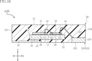
- FIG. 16 is a cross-sectional view taken along line XVI--XVI of FIG. 14.
- FIG. 17 is a cross-sectional view along line XVII-XVII of FIG. 14.
- FIG. 18 is a plan view of a semiconductor device according to a fourth embodiment of the present disclosure
- FIG. 19 is a bottom view of the semiconductor device shown in FIG. 18.
- FIG. 20 is a left side view of the semiconductor device shown in FIG. 18.
- FIG. 21 is a cross-sectional view taken along line XXI-XXI of FIG. 18.
- FIG. 22 is a cross-sectional view along line XXII-XXII of FIG. 18.
- FIG. 23 is a plan view of a semiconductor device according to a fifth embodiment of the present disclosure;
- FIG. FIG. 24 is a plan view corresponding to FIG. 23, showing the sealing resin through.
- 25 is a cross-sectional view taken along line XXV--XXV of FIG. 24.
- FIG. 26 is a cross-sectional view taken along line XXVI--XXVI of FIG. 24.
- FIG. 27 is a cross-sectional view along line XXVII-XXVII of FIG
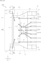
- FIG. 1 A semiconductor device A10 according to the first embodiment of the present disclosure will be described based on FIGS. 1 to 8.
- the semiconductor device A10 is used, for example, for monitoring the voltage of a battery mounted on an electric vehicle.
- the package format of the semiconductor device A10 is a QFN (Quad Flat Non-leaded package).
- the semiconductor device A10 includes a die pad 10, a first terminal 21, a second terminal 22, a plurality of third terminals 23, two fourth terminals 24, a first semiconductor element 31, a second semiconductor element 32, and a sealing resin 50.
- FIG. 2 shows the encapsulation resin 50 in a transparent manner for convenience of understanding.
- an imaginary line indicates the outline of the encapsulating resin 50 that is transmitted through.
- the VI-VI line is indicated by a one-dot chain line.
- first direction x A direction in which the first terminal 21 and the second terminal 22 are separated is called "first direction x”.
- second direction y A direction perpendicular to the first direction x is called a “second direction y”.
- third direction z A direction orthogonal to the first direction x and the second direction y is called a “third direction z”.
- the third direction z corresponds to the normal direction of the top surface 51 of the sealing resin 50, which will be described later.
- the sealing resin 50 includes the die pad 10, the first semiconductor element 31, the second semiconductor element 32, the first terminal 21, the second terminal 22, the plurality of third terminals 23, and the It partially covers each of the two fourth terminals 24 .
- the sealing resin 50 has electrical insulation.
- Sealing resin 50 includes, for example, black epoxy resin.
- the sealing resin 50 has a top surface 51 , a bottom surface 52 , a first side surface 531 , a second side surface 532 , a third side surface 533 and a fourth side surface 534 .
- the bottom surface 52 faces one side in the third direction z.
- the top surface 51 faces the side opposite to the bottom surface 52 in the third direction z.
- the first side surface 531 faces one side in the second direction y.
- the first side surface 531 is located closest to the first terminal 21 and the second terminal 22 in the second direction y.
- the second side surface 532 faces one side in the first direction x.
- the second side surface 532 is located closest to the first terminal 21 in the first direction x.
- the third side surface 533 faces the side opposite to the second side surface 532 in the first direction x.
- the fourth side surface 534 faces the side opposite to the first side surface 531 in the second direction y.
- a first side surface 531 , a second side surface 532 , a third side surface 533 and a fourth side surface 534 are connected to the bottom surface 52 .
- the first side surface 531 , the second side surface 532 , the third side surface 533 and the fourth side surface 534 are also connected to the top surface 51 .
- the die pad 10 is located between the first terminal 21 and the second terminal 22 in the first direction x, as shown in FIG.
- Die pad 10 contains a metal element.
- the metal element is, for example, copper (Cu).
- the die pad 10, the first terminal 21, the second terminal 22, the plurality of third terminals 23 and the two fourth terminals 24 are obtained from the same terminal frame.
- die pad 10 has mounting surface 11 and first edge 12 .
- the mounting surface 11 faces the same side as the top surface 51 of the sealing resin 50 in the third direction z.
- the first edge 12 extends in the first direction x and is located closest to the first side surface 531 of the sealing resin 50 .
- the dimension of the die pad 10 in the first direction x increases toward the side opposite to the side on which the first side surface 531 of the sealing resin 50 is located with respect to the first semiconductor element 31 in the second direction y. expands. Furthermore, the portion of the die pad 10 located on the opposite side of the first edge 12 with respect to the first semiconductor element 31 in the second direction y protrudes on both sides of the first edge 12 with respect to the first direction x. As shown in FIGS. 6 and 7 , the die pad 10 is positioned away from the bottom surface 52 of the sealing resin 50 .
- the first terminal 21 is positioned away from the first side surface 531 of the sealing resin 50, as shown in FIG. As shown in FIGS. 2 and 3, the first terminal 21 is positioned on one side of the first edge 12 of the die pad 10 in the first direction x. In the semiconductor device A10, the first terminal 21 is located on the side opposite to the fourth side surface 534 of the sealing resin 50 with respect to the first edge 12 in the second direction y. Further, the first terminal 21 is located apart from a first extension line L1 extending from one end of the first edge 12 in the first direction x.
- the first terminal 21 has a first main surface 211, a first back surface 212 and a first end surface 213.
- the first main surface 211 faces the same side as the top surface 51 of the sealing resin 50 in the third direction z.
- the first main surface 211 is covered with the sealing resin 50.
- the first rear surface 212 faces the side opposite to the first main surface 211 in the third direction z.
- the first rear surface 212 is exposed to the outside from the bottom surface 52 of the sealing resin 50 .
- the first end surface 213 faces the same side as the second side surface 532 of the sealing resin 50 in the first direction x.
- the first end surface 213 is exposed to the outside from the second side surface 532 .
- the second terminal 22 is positioned away from the first side surface 531 of the sealing resin 50, as shown in FIG.
- the second terminal 22 is positioned apart from the first terminal 21 in the first direction x.
- the second terminal 22 is located on the opposite side of the first terminal 21 with respect to the first edge 12 of the die pad 10 in the first direction x. Therefore, the first terminal 21 and the second terminal 22 are positioned on both sides of the first edge 12 in the first direction x.
- the second terminal 22 is located on the side opposite to the fourth side surface 534 of the sealing resin 50 with respect to the first edge 12 in the second direction y. Further, the second terminal 22 is located apart from a second extension line L2 extending from the other end of the first edge 12 in the first direction x.
- the second terminal 22 has a second main surface 221, a second rear surface 222 and a second end surface 223.
- the second main surface 221 faces the same side as the top surface 51 of the sealing resin 50 in the third direction z.
- the second main surface 221 is covered with the sealing resin 50.
- the second rear surface 222 faces the side opposite to the second main surface 221 in the third direction z.
- the second rear surface 222 is exposed to the outside from the bottom surface 52 of the sealing resin 50 .
- the second end surface 223 faces the same side as the third side surface 533 of the sealing resin 50 in the second direction y.
- the second end surface 223 is exposed outside from the third side surface 533 .
- the plurality of third terminals 23 are located on the side opposite to the first side surface 531 of the sealing resin 50 with the die pad 10 as a reference in the second direction y.
- the multiple third terminals 23 are arranged along the first direction x.
- the interval between two third terminals 23 adjacent in the first direction x is shorter than the interval between the first terminal 21 and the second terminal 22 .
- the multiple third terminals 23 include an A terminal 23A, a B terminal 23B, two C terminals 23C, and multiple D terminals 23D.
- the plurality of third terminals 23 have a third main surface 231, a third rear surface 232 and a third end surface 233.
- the third main surface 231 faces the same side as the top surface 51 of the sealing resin 50 in the third direction z.
- the third main surface 231 is covered with the sealing resin 50.
- the third rear surface 232 faces the side opposite to the third main surface 231 in the third direction z.
- the third back surface 232 is exposed to the outside from the bottom surface 52 of the sealing resin 50 .
- the third end surface 233 faces the same side as the fourth side surface 534 of the sealing resin 50 in the second direction y. As shown in FIG. 5 , the third end face 233 is exposed outside from the fourth side face 534 .
- the two fourth terminals 24 are positioned apart from each other in the first direction x and support the die pad 10, as shown in FIG.
- a plurality of third terminals 23 are positioned between two fourth terminals 24 in the first direction x.
- the two fourth terminals 24 have a fourth main surface 241, a fourth rear surface 242, a fourth end surface 243 and a connecting surface 244.
- the fourth main surface 241 faces the same side as the top surface 51 of the sealing resin 50 in the third direction z.
- the fourth main surface 241 is covered with the sealing resin 50.
- the fourth rear surface 242 faces the side opposite to the third main surface 231 in the third direction z.
- the fourth rear surface 242 is exposed to the outside from the bottom surface 52 of the sealing resin 50 .
- the fourth end surface 243 faces the same side as the fourth side surface 534 of the sealing resin 50 in the second direction y. As shown in FIG.
- the fourth end surface 243 is exposed to the outside from the fourth side surface 534 .
- the connecting surface 244 connects the fourth main surface 241 and the mounting surface 11 of the die pad 10 .
- the connecting surface 244 is inclined with respect to the fourth principal surface 241 and the mounting surface 11 .
- the connecting surface 244 is covered with the sealing resin 50 .
- the first semiconductor element 31 and the second semiconductor element 32 are mounted on the mounting surface 11 of the die pad 10, as shown in FIGS. Both the first semiconductor element 31 and the second semiconductor element 32 are integrated circuits (ICs).
- the second semiconductor element 32 is positioned between the first semiconductor element 31 and the plurality of third terminals 23 in the second direction y. As shown in FIG. 7, the first semiconductor element 31 and the second semiconductor element 32 are bonded to the mounting surface 11 via the bonding layer 39 .
- the bonding layer 39 is made of, for example, a paste containing silver-containing epoxy resin as a main component (so-called Ag paste).
- the first semiconductor element 31 has multiple first electrodes 311 .
- the multiple first electrodes 311 are electrically connected to the circuit configured in the first semiconductor element 31 .
- the second semiconductor element 32 has a plurality of second electrodes 321 .
- the multiple second electrodes 321 are electrically connected to the circuit configured in the second semiconductor element 32 .
- the semiconductor device A10 further includes two first wires 41, a plurality of second wires 42, a plurality of third wires 43, and a plurality of fourth wires 44.
- the composition of these wires includes gold (Au), for example. These wires are covered with a sealing resin 50 .
- the two first wires 41 are connected to the two first electrodes 311 of the first semiconductor element 31, the first main surface 211 of the first terminal 21, and the second main surface of the second terminal 22. 221 separately. Thereby, the first terminal 21 and the second terminal 22 are electrically connected to the first semiconductor element 31 .
- the plurality of second wires 42 are connected to the two first electrodes 311 of the first semiconductor element 31, the third main surface 231 of the A terminal 23A, and the third main surface 231 of the B terminal 23B. are individually bonded to the Thereby, the first semiconductor element 31 is electrically connected to the A terminal 23A and the B terminal 23B.
- the multiple third wires 43 are individually joined to the multiple first electrodes 311 of the first semiconductor element 31 and the multiple second electrodes 321 of the second semiconductor element 32 .
- the second semiconductor element 32 is electrically connected to the first semiconductor element 31 .
- the plurality of fourth wires 44 are connected to the plurality of second electrodes 321 of the second semiconductor element 32, the third main surfaces 231 of the two C terminals 23C, and the third main surfaces 231 of the plurality of D terminals 23D. It is individually bonded to the main surface 231 . Thereby, the second semiconductor element 32 is electrically connected to the two C terminals 23C and the plurality of D terminals 23D.
- the sealing resin 50 is provided with a plurality of recesses 55.
- the plurality of recesses 55 are positioned between the first terminal 21 and the second terminal 22 in the first direction x. As shown in FIGS. 6 and 7, the recesses 55 overlap the first terminals 21 and the second terminals 22 when viewed in the first direction x.
- a plurality of recesses 55 are recessed from the bottom surface 52 and connected to the first side surface 531 .
- the multiple recesses 55 extend in the second direction y. In the semiconductor device A10, the recesses 55 are located away from the die pad 10 when viewed in the third direction z.
- the dimension H of each of the plurality of recesses 55 in the third direction z is greater than the dimensions H1 and H2 of each of the first terminal 21 and the second terminal 22 in the third direction z. .
- a step-down circuit is configured in the first semiconductor element 31 .
- the step-down circuit includes a plurality of resistive elements.
- the first terminal 21 and the second terminal 22 are connected to a battery (not shown) to be monitored.
- the first terminal 21 is a positive electrode.
- the second terminal 22 is the negative electrode.
- the voltage of the battery applied to the first terminal 21 and the second terminal 22 is converted into a weak electrical signal by the step-down circuit of the first semiconductor element 31 .
- the second semiconductor element 32 includes two operational amplifiers OP1 and OP2. However, the second semiconductor element 32 may be configured without the operational amplifier OP2.
- the operational amplifier OP1 amplifies the weak electric signal converted by the first semiconductor element 31 and outputs the amplified signal to the A terminal 23A through the first semiconductor element 31. FIG. This allows the voltage of the battery to be monitored.
- the B terminal 23B is for grounding the first semiconductor element 31 .
- a power supply for driving the second semiconductor element 32 is connected to the two C terminals 23C.
- a plurality of D terminals 23D are electrically connected to the operational amplifier OP2.
- An electrical signal generated by another control circuit (not shown) based on the electrical signal output from the A terminal 23A is input to the operational amplifier OP2.
- high-frequency noise contained in the electrical signal output from the A terminal 23A is removed by the operational amplifier OP2, and monitoring can be performed with higher accuracy.
- the semiconductor device A10 includes a sealing resin 50 that partially covers each of the first terminals 21 and the second terminals 22, and a second terminal that is electrically connected to the first terminals 21 and the second terminals 22 and covered with the sealing resin 50.
- 1 semiconductor element 31 The second terminal 22 is positioned apart from the first terminal 21 in the first direction x.
- the sealing resin 50 has a first side surface 531 facing the second direction y and located closest to the first terminal 21 and the second terminal 22 in the second direction y.
- the first terminal 21 and the second terminal 22 are located away from the first side surface 531 .
- the semiconductor device A10 further includes a die pad 10 on which the first semiconductor element 31 is mounted. As viewed in the third direction z, the die pad 10 has a first edge 12 extending in the first direction x. The first edge 12 is positioned closest to the first side surface 531 of the sealing resin 50 . The first terminal 21 and the second terminal 22 are positioned on both sides of the first edge 12 in the first direction x. By adopting this configuration, the distances between the plurality of third terminals 23 and the first terminals 21 and the second terminals 22 are sufficiently secured. It is possible to suppress the discharge between the plurality of third terminals 23 and the first terminals 21 and the second terminals 22 are sufficiently secured. It is possible to suppress the discharge between
- the sealing resin 50 is provided with a concave portion 55 located between the first terminal 21 and the second terminal 22 in the first direction x.
- the recess 55 is recessed from the bottom surface 52 of the sealing resin 50 .
- the concave portion 55 overlaps the first terminal 21 and the second terminal 22 when viewed in the first direction x.
- the recess 55 extends in the second direction y. Furthermore, the dimension H of the recess 55 in the third direction z is larger than the dimensions H1 and H2 of the first terminal 21 and the second terminal 22 in the third direction z (see FIG. 8). As a result, when viewed in the first direction x, the entirety of each of the first terminal 21 and the second terminal 22 overlaps with the recess 55 (see FIGS. 6 and 7). Therefore, discharge between the first terminal 21 and the second terminal 22 can be suppressed more effectively.
- the semiconductor device A10 further includes two fourth terminals 24 positioned apart from each other in the first direction x and supporting the die pad 10 .
- the two fourth terminals 24 are located apart from the second side surface 532 and the third side surface 533 of the sealing resin 50 .
- a plurality of third terminals 23 are positioned between two fourth terminals 24 in the first direction x.
- the dimension of the die pad 10 in the first direction x increases toward the side opposite to the side where the first side surface 531 of the sealing resin 50 is located with respect to the first semiconductor element 31 in the second direction y. Furthermore, the portion of the die pad 10 located on the opposite side of the first edge 12 with respect to the first semiconductor element 31 in the second direction y protrudes on both sides of the first edge 12 with respect to the first direction x.
- the interval between the two fourth terminals 24 can be made longer, so the interval between the two adjacent third terminals 23 can be set longer. This makes it possible to reduce mutual interference of noise in the plurality of third terminals 23 .
- the first terminal 21 is exposed outside from the second side surface 532 of the sealing resin 50 .
- the second terminal 22 is exposed outside from the third side surface 533 of the sealing resin 50 .
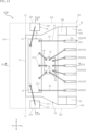
- FIG. 10 shows the encapsulation resin 50 in a transparent manner for convenience of understanding.
- the outline of the encapsulating resin 50 that is transmitted through is indicated by imaginary lines.
- the semiconductor device A20 differs from the semiconductor device A10 in the configuration of the first terminals 21 and the second terminals 22 and the configuration of the plurality of concave portions 55 provided in the sealing resin 50 .
- the first terminal 21 when viewed in the third direction z, overlaps the first extension line L1 extending from one end of the first edge 12 of the die pad 10 in the first direction x.
- the second terminal 22 overlaps the second extension line L2 extending from the other end of the first edge 12 of the die pad 10 when viewed in the third direction z.
- the recesses 55 overlap the die pad 10 when viewed in the third direction z. As a result, the recesses 55 overlap the first terminals 21 and the second terminals 22 when viewed in the first direction x.
- the dimension H of each of the plurality of recesses 55 in the third direction z is smaller than the dimensions H1 and H2 of each of the first terminal 21 and the second terminal 22 in the third direction z.
- the semiconductor device A20 includes a sealing resin 50 that partially covers each of the first terminals 21 and the second terminals 22, and a second terminal that is electrically connected to the first terminals 21 and the second terminals 22 and covered with the sealing resin 50.
- 1 semiconductor element 31 The second terminal 22 is positioned apart from the first terminal 21 in the first direction x.
- the sealing resin 50 has a first side surface 531 facing the second direction y and located closest to the first terminal 21 and the second terminal 22 in the second direction y.
- the first terminal 21 and the second terminal 22 are located away from the first side surface 531 . Therefore, according to this configuration, even in the semiconductor device A20, it is possible to reduce the size of the device while suppressing the discharge between the plurality of terminals. Furthermore, since the semiconductor device A20 has the same configuration as the semiconductor device A10, the semiconductor device A20 also exhibits the effects of the configuration.
- the first terminal 21 when viewed in the third direction z, overlaps the first extension line L1 extending from one end of the first edge 12 of the die pad 10 in the first direction x.
- the second terminal 22 overlaps the second extension line L2 extending from the other end of the first edge 12 of the die pad 10 when viewed in the third direction z.
- the recess 55 overlaps the die pad 10 when viewed in the third direction z.
- the concave portion 55 overlaps the first terminal 21 and the second terminal 22 when viewed in the first direction x. Therefore, the creeping distance of the sealing resin 50 from the first terminal 21 to the second terminal 22 via the bottom surface 52 is equivalent to the distance of the semiconductor device A10. Discharge between the two terminals 22 can be effectively suppressed.
- FIG. 14 shows the encapsulation resin 50 in a transparent manner for convenience of understanding.
- the outline of the encapsulating resin 50 that is transmitted through is indicated by imaginary lines.
- the XVII-XVII line is indicated by a dashed line.
- the semiconductor device A30 differs from the semiconductor device A10 in the configuration of the first terminals 21 and the second terminals 22 and the configuration of the plurality of concave portions 55 provided in the sealing resin 50 .
- the first terminal 21 and the second terminal 22 are located in the second direction y with the first edge 12 of the die pad 10 as a reference. 1 side 531 is located on the opposite side. Therefore, the first terminal 21 is located away from the first extension line L1 extending from one end of the first edge 12 of the die pad 10 in the first direction x.
- the second terminal 22 is positioned away from the second extension line L2 extending from the other end of the first edge 12 of the die pad 10 .
- the recesses 55 overlap the die pad 10 when viewed in the third direction z. As a result, the recesses 55 overlap the first terminals 21 and the second terminals 22 when viewed in the first direction x.
- the dimension H of each of the plurality of recesses 55 in the third direction z is smaller than the dimensions H1 and H2 of each of the first terminal 21 and the second terminal 22 in the third direction z.
- the semiconductor device A30 includes a sealing resin 50 that partially covers each of the first terminals 21 and the second terminals 22, and a second terminal that is electrically connected to the first terminals 21 and the second terminals 22 and covered with the sealing resin 50.
- 1 semiconductor element 31 The second terminal 22 is positioned apart from the first terminal 21 in the first direction x.
- the sealing resin 50 has a first side surface 531 facing the second direction y and located closest to the first terminal 21 and the second terminal 22 in the second direction y.
- the first terminal 21 and the second terminal 22 are located away from the first side surface 531 . Therefore, according to this configuration, even in the semiconductor device A30, it is possible to reduce the size of the device while suppressing discharge between a plurality of terminals. Further, since the semiconductor device A30 has the same configuration as the semiconductor device A10, the semiconductor device A30 also exhibits the effects of the configuration.
- the first terminal 21 and the second terminal 22 are aligned with the first side surface 531 of the sealing resin 50 with the first edge 12 of the die pad 10 as a reference in the second direction y. are located on the opposite side.
- the creepage distance of the sealing resin 50 from the first terminal 21 to the second terminal 22 via the first side surface 531 becomes longer than the configuration of the semiconductor device A20 described above. Therefore, the effect of suppressing discharge between a plurality of terminals becomes even higher than in the case of the semiconductor device A10.
- FIG. 18 A semiconductor device A40 according to the fourth embodiment of the present disclosure will be described with reference to FIGS. 18 to 22.
- FIG. 18 the same or similar elements as those of the semiconductor device A10 described above are denoted by the same reference numerals, and overlapping descriptions are omitted.
- the XXI-XXI line is indicated by a dashed line.
- the semiconductor device A40 differs from the semiconductor device A10 in the configuration of the plurality of concave portions 55 provided in the sealing resin 50 .
- the multiple recesses 55 are recessed from the first side surface 531 of the sealing resin 50. As shown in FIGS. The plurality of recesses 55 are connected to the top surface 51 of the sealing resin 50 and the bottom surface 52 of the sealing resin 50 . The recesses 55 overlap the first terminal 21 and the second terminal 22 when viewed in the first direction x.
- the dimension H of the recesses 55 in the third direction z is greater than the dimensions H1 and H2 of the first terminal 21 and the second terminal 22 in the third direction z.
- dimension H is equal to the distance between top surface 51 and bottom surface 52 .
- the semiconductor device A40 includes a sealing resin 50 that partially covers each of the first terminals 21 and the second terminals 22, and a second terminal that is electrically connected to the first terminals 21 and the second terminals 22 and covered with the sealing resin 50.
- 1 semiconductor element 31 The second terminal 22 is positioned apart from the first terminal 21 in the first direction x.
- the sealing resin 50 has a first side surface 531 facing the second direction y and located closest to the first terminal 21 and the second terminal 22 in the second direction y.
- the first terminal 21 and the second terminal 22 are located away from the first side surface 531 . Therefore, according to this configuration, even in the semiconductor device A40, it is possible to reduce the size of the device while suppressing discharge between a plurality of terminals. Further, since the semiconductor device A40 has the same configuration as the semiconductor device A10, the semiconductor device A40 also has the effect of the configuration.
- FIG. 24 shows the encapsulation resin 50 in a transparent manner for convenience of understanding.
- the outline of the encapsulation resin 50 seen through is shown by imaginary lines.
- the XXVI-XXVI line and the XXVII-XXVII line are each indicated by a dashed line.
- the semiconductor device A50 differs from the semiconductor device A10 in the configuration of the die pad 10, the first terminal 21, the second terminal 22, the plurality of third terminals 23, and the two fourth terminals 24.
- the package format of the semiconductor device A50 is SOP (Small Outline Package).
- the plurality of concave portions 55 are not provided in the sealing resin 50. As shown in FIG.
- the die pad 10 includes a first pad 10A and a second pad 10B.
- the second pads 10B are positioned between the first pads 10A and the plurality of third terminals 23 in the second direction y.
- the first semiconductor element 31 is mounted on the mounting surface 11 of the first pad 10A.
- the second semiconductor element 32 is mounted on the mounting surface 11 of the second pad 10B.
- the second terminal 22 is connected to the first pad 10A.
- the two fourth terminals 24 are connected to the second pads 10B.
- a first edge 12 is included in the first pad 10A.
- the first terminal 21 protrudes from the second side surface 532 of the sealing resin 50.
- the second terminal 22 protrudes from the third side surface 533 of the sealing resin 50 .
- a portion of each of the first terminal 21 and the second terminal 22 protruding from the sealing resin 50 is bent toward the side where the bottom surface 52 of the sealing resin 50 is located in the third direction z.
- a part of each of the first main surface 211 of the first terminal 21 and the second main surface 221 of the second terminal 22 is covered with the sealing resin 50 .
- the plurality of third terminals 23 and the two fourth terminals 24 protrude from the fourth side surface 534 of the sealing resin 50. As shown in FIG. Portions of each of the plurality of third terminals 23 and the two fourth terminals 24 protruding from the sealing resin 50 are bent toward the side where the bottom surface 52 of the sealing resin 50 is located in the third direction z.
- the first terminals 21 and the second terminals 22 are located apart from the first side surface 531 of the sealing resin 50 . Also in the semiconductor device A50, the first terminal 21 and the second terminal 22 are positioned on both sides of the first edge 12 of the first pad 10A in the first direction x. Further, in the semiconductor device A50, the first terminal 21 and the second terminal 22 are located on the opposite side of the first side surface 531 with the first edge 12 as a reference in the second direction y.
- the semiconductor device A50 includes a sealing resin 50 that partially covers each of the first terminals 21 and the second terminals 22, and a second terminal that is electrically connected to the first terminals 21 and the second terminals 22 and covered with the sealing resin 50.
- 1 semiconductor element 31 The second terminal 22 is positioned apart from the first terminal 21 in the first direction x.
- the sealing resin 50 has a first side surface 531 facing the second direction y and located closest to the first terminal 21 and the second terminal 22 in the second direction y.
- the first terminal 21 and the second terminal 22 are located away from the first side surface 531 . Therefore, according to this configuration, even in the semiconductor device A50, it is possible to reduce the size of the device while suppressing the discharge between the plurality of terminals. Furthermore, since the semiconductor device A50 has the same configuration as the semiconductor device A10, the semiconductor device A50 also exhibits the effects of the configuration.
- Appendix 1 a first semiconductor element; a first terminal electrically connected to the first semiconductor element; a second terminal electrically connected to the first semiconductor element and positioned away from the first terminal in a first direction; a part of each of the first terminal and the second terminal, the first semiconductor element, and a sealing resin covering the terminal; the sealing resin has a first side surface facing a second direction orthogonal to the first direction and positioned closest to the first terminal and the second terminal in the second direction; The semiconductor device, wherein the first terminal and the second terminal are located away from the first side surface.
- the die pad When viewed in a third direction orthogonal to the first direction and the second direction, the die pad extends in the first direction and is located closest to the first side surface in the second direction. having an edge,
- the semiconductor device according to appendix 1 wherein the first terminal and the second terminal are positioned on both sides of the first edge in the first direction.
- Appendix 3. The semiconductor device according to appendix 2, wherein the first terminal and the second terminal are positioned on the opposite side of the first side surface with respect to the first edge in the second direction.
- Appendix 4. The semiconductor device according to appendix 2, wherein the first terminal overlaps a first extension line extending in the first direction from one end of the first edge when viewed in the third direction.
- the sealing resin has a bottom surface facing the side opposite to the side on which the first semiconductor element is positioned with respect to the die pad, 8.
- the sealing resin is provided with a recess positioned between the first terminal and the second terminal in the first direction, The semiconductor device according to appendix 8, wherein the recess overlaps the first terminal and the second terminal when viewed in the first direction.
- Appendix 10 The semiconductor device according to appendix 9, wherein the recess is recessed from the bottom surface and extends in the second direction. Appendix 11.
- the sealing resin has a second side surface and a third side surface facing opposite to each other in the first direction, The first terminal is exposed to the outside from the second side surface, 4.
- Appendix 13 The first terminal protrudes from the second side surface, 13.
- the semiconductor device according to any one of appendices 2 to 13, wherein the first semiconductor element includes a step-down circuit including a plurality of resistance elements.
- Appendix 15. a second semiconductor device including an operational amplifier; further comprising a plurality of third terminals electrically connected to the second semiconductor element; the second semiconductor element is electrically connected to the first semiconductor element; a part of each of the plurality of third terminals and the second semiconductor element are covered with the sealing resin; 15.
- Appendix 16. 16 The semiconductor device according to appendix 15, wherein the second semiconductor element is mounted on the die pad. Appendix 17.
Landscapes
- Engineering & Computer Science (AREA)
- Microelectronics & Electronic Packaging (AREA)
- Power Engineering (AREA)
- Physics & Mathematics (AREA)
- Condensed Matter Physics & Semiconductors (AREA)
- General Physics & Mathematics (AREA)
- Computer Hardware Design (AREA)
- Structures Or Materials For Encapsulating Or Coating Semiconductor Devices Or Solid State Devices (AREA)
Abstract
半導体装置は、第1半導体素子と、前記第1半導体素子に導通する第1端子と、前記第1半導体素子に導通するとともに、第1方向において前記第1端子から離れて位置する第2端子と、前記第1端子および前記第2端子の各々の一部ならびに前記第1半導体素子を覆う封止樹脂と、を備える。前記封止樹脂は、前記第1方向に対して直交する第2方向を向き、かつ前記第2方向において前記第1端子および前記第2端子から最も近くに位置する第1側面を有する。前記第1端子および前記第2端子は、前記第1側面から離れて位置する。
Description
本開示は、半導体装置に関する。
近年、電気自動車が普及しつつある。特許文献1には、電気自動車に搭載されたバッテリの電圧をモニタリングし、かつインバータを制御するための回路の一例が開示されている。当該回路により、モータを駆動するためのインバータに過電圧が供給されるのを防止できる。
特許文献1に開示されている回路のうち、電気自動車に搭載されたバッテリの電圧をモニタリングするために必要な回路は、抵抗電圧検出回路および高電圧バッテリ検出回路である。これら2つの回路は、複数のICで構成される。ここで、これら2つの回路をできるだけ少ない数のICでまとめて、かつ当該ICに導通する複数の端子を具備する単一の半導体装置とすれば、特許文献1に開示されている回路がよりコンパクトなものとなる。しかし、当該半導体装置の複数の端子のうちバッテリに接続される複数の端子には、高電圧が印加されることとなる。したがって、当該半導体装置に対してさらなる小型化を図ろうとすると複数の端子の間隔がより短くなるため、高電圧が印加される複数の端子の間で放電が発生するおそれがある。
本開示は、従来よりも改良が施された半導体装置を提供することを一の課題とする。特に本開示は、上記事情に鑑み、装置の小型化を図りつつ、複数の端子の間での放電を抑制することが可能な半導体装置を提供することを一の課題とする。
本開示の第1の側面によって提供される半導体装置は、第1半導体素子と、前記第1半導体素子に導通する第1端子と、前記第1半導体素子に導通するとともに、第1方向において前記第1端子から離れて位置する第2端子と、前記第1端子および前記第2端子の各々の一部ならびに前記第1半導体素子を覆う封止樹脂と、を備える。前記封止樹脂は、前記第1方向に対して直交する第2方向を向き、かつ前記第2方向において前記第1端子および前記第2端子から最も近くに位置する第1側面を有する。前記第1端子および前記第2端子は、前記第1側面から離れて位置する。
上記構成によれば、半導体装置の小型化を図りつつ、複数の端子の間での放電を抑制することが可能となる。
本開示のその他の特徴および利点は、添付図面に基づき以下に行う詳細な説明によって、より明らかとなろう。
本開示を実施するための形態について、添付図面に基づいて説明する。
第1実施形態:
図1~図8に基づき、本開示の第1実施形態にかかる半導体装置A10について説明する。半導体装置A10は、たとえば、電気自動車に搭載されたバッテリの電圧のモニタリングに使用される。半導体装置A10のパッケージ形式は、QFN(Quad Flat Non-leaded package)である。半導体装置A10は、ダイパッド10、第1端子21、第2端子22、複数の第3端子23、2つの第4端子24、第1半導体素子31、第2半導体素子32および封止樹脂50を備える。ここで、図2は、理解の便宜上、封止樹脂50を透過して示している。図2において透過した封止樹脂50の外形を想像線(二点鎖線)で示している。図2において、VI-VI線を一点鎖線で示している。
図1~図8に基づき、本開示の第1実施形態にかかる半導体装置A10について説明する。半導体装置A10は、たとえば、電気自動車に搭載されたバッテリの電圧のモニタリングに使用される。半導体装置A10のパッケージ形式は、QFN(Quad Flat Non-leaded package)である。半導体装置A10は、ダイパッド10、第1端子21、第2端子22、複数の第3端子23、2つの第4端子24、第1半導体素子31、第2半導体素子32および封止樹脂50を備える。ここで、図2は、理解の便宜上、封止樹脂50を透過して示している。図2において透過した封止樹脂50の外形を想像線(二点鎖線)で示している。図2において、VI-VI線を一点鎖線で示している。
半導体装置A10の説明においては、便宜上、第1端子21と第2端子22とが離れる方向を「第1方向x」と呼ぶ。第1方向xに対して直交する方向を「第2方向y」と呼ぶ。第1方向xおよび第2方向yに対して直交する方向を「第3方向z」と呼ぶ。第3方向zは、後述する封止樹脂50の頂面51の法線方向に相当する。
封止樹脂50は、図6~図8に示すように、ダイパッド10、第1半導体素子31および第2半導体素子32と、第1端子21、第2端子22、複数の第3端子23、および2つの第4端子24の各々の一部ずつとを覆っている。封止樹脂50は、電気絶縁性を有する。封止樹脂50は、たとえば黒色のエポキシ樹脂を含む。図1および図3に示すように、封止樹脂50は、頂面51、底面52、第1側面531、第2側面532、第3側面533および第4側面534を有する。
図6~図8に示すように、底面52は、第3方向zの一方側を向く。頂面51は、第3方向zにおいて底面52とは反対側を向く。
図6および図7に示すように、第1側面531は、第2方向yの一方側を向く。第1側面531は、第2方向yにおいて第1端子21および第2端子22から最も近くに位置する。第2側面532は、第1方向xの一方側を向く。第2側面532は、第1方向xにおいて第1端子21から最も近くに位置する。第3側面533は、第1方向xにおいて第2側面532とは反対側を向く。第4側面534は、第2方向yにおいて第1側面531とは反対側を向く。第1側面531、第2側面532、第3側面533および第4側面534は、底面52につながっている。さらに第1側面531、第2側面532、第3側面533および第4側面534は、頂面51にもつながっている。
ダイパッド10は、図2に示すように、第1方向xにおいて第1端子21と第2端子22との間に位置する。ダイパッド10は、金属元素を含む。当該金属元素は、たとえば銅(Cu)である。ダイパッド10、第1端子21、第2端子22、複数の第3端子23、および2つの第4端子24は、同一の端子フレームから得られる。図1および図2に示すように、ダイパッド10は、搭載面11および第1縁12を有する。搭載面11は、第3方向zにおいて封止樹脂50の頂面51と同じ側を向く。第3方向zに視て、第1縁12は、第1方向xに延び、かつ封止樹脂50の第1側面531から最も近くに位置する。
図2に示すように、第2方向yにおいて第1半導体素子31を基準として封止樹脂50の第1側面531が位置する側とは反対側に向かうほど、ダイパッド10の第1方向xの寸法が拡大する。さらに、第2方向yにおいて第1半導体素子31を基準として第1縁12とは反対側に位置するダイパッド10の部位は、第1縁12を基準として第1方向xの両側にはみ出している。図6および図7に示すように、ダイパッド10は、封止樹脂50の底面52から離れて位置する。
第1端子21は、図1に示すように、封止樹脂50の第1側面531から離れて位置する。図2および図3に示すように、第1端子21は、ダイパッド10の第1縁12の第1方向xの一方側に位置する。半導体装置A10においては、第1端子21は、第2方向yにおいて第1縁12を基準として封止樹脂50の第4側面534とは反対側に位置する。さらに第1端子21は、第1縁12の一端から第1方向xに延びる第1延長線L1から離れて位置する。
図2、図3および図8に示すように、第1端子21は、第1主面211、第1裏面212および第1端面213を有する。第1主面211は、第3方向zにおいて封止樹脂50の頂面51と同じ側を向く。半導体装置A10においては、第1主面211は、封止樹脂50に覆われている。第1裏面212は、第3方向zにおいて第1主面211とは反対側を向く。第1裏面212は、封止樹脂50の底面52から外部に露出している。第1端面213は、第1方向xにおいて封止樹脂50の第2側面532と同じ側を向く。第1端面213は、第2側面532から外部に露出している。
第2端子22は、図1に示すように、封止樹脂50の第1側面531から離れて位置する。第2端子22は、第1方向xにおいて第1端子21から離れて位置する。図2および図3に示すように、第2端子22は、第1方向xにおいてダイパッド10の第1縁12を基準として第1端子21とは反対側に位置する。したがって、第1端子21および第2端子22は、第1縁12の第1方向xの両側に位置する。第2端子22は、第2方向yにおいて第1縁12を基準として封止樹脂50の第4側面534とは反対側に位置する。さらに第2端子22は、第1縁12の他端から第1方向xに延びる第2延長線L2から離れて位置する。
図2、図3および図8に示すように、第2端子22は、第2主面221、第2裏面222および第2端面223を有する。第2主面221は、第3方向zにおいて封止樹脂50の頂面51と同じ側を向く。半導体装置A10においては、第2主面221は、封止樹脂50に覆われている。第2裏面222は、第3方向zにおいて第2主面221とは反対側を向く。第2裏面222は、封止樹脂50の底面52から外部に露出している。第2端面223は、第2方向yにおいて封止樹脂50の第3側面533と同じ側を向く。第2端面223は、第3側面533から外部に露出している。
複数の第3端子23は、図2に示すように、第2方向yにおいてダイパッド10を基準として封止樹脂50の第1側面531とは反対側に位置する。複数の第3端子23は、第1方向xに沿って配列されている。第1方向xにおいて隣り合う2つの第3端子23の間隔は、第1端子21と第2端子22との間隔よりも短い。複数の第3端子23は、A端子23A、B端子23B、2つのC端子23C、および複数のD端子23Dを含む。
図2、図3および図7に示すように、複数の第3端子23は、第3主面231、第3裏面232および第3端面233を有する。第3主面231は、第3方向zにおいて封止樹脂50の頂面51と同じ側を向く。半導体装置A10においては、第3主面231は、封止樹脂50に覆われている。第3裏面232は、第3方向zにおいて第3主面231とは反対側を向く。第3裏面232は、封止樹脂50の底面52から外部に露出している。第3端面233は、第2方向yにおいて封止樹脂50の第4側面534と同じ側を向く。図5に示すように、第3端面233は、第4側面534から外部に露出している。
2つの第4端子24は、図2に示すように、第1方向xにおいて互いに離れて位置し、かつダイパッド10を支持している。複数の第3端子23は、第1方向xにおいて2つの第4端子24の間に位置する。
図2、図3および図6に示すように、2つの第4端子24は、第4主面241、第4裏面242、第4端面243および連結面244を有する。第4主面241は、第3方向zにおいて封止樹脂50の頂面51と同じ側を向く。半導体装置A10においては、第4主面241は、封止樹脂50に覆われている。第4裏面242は、第3方向zにおいて第3主面231とは反対側を向く。第4裏面242は、封止樹脂50の底面52から外部に露出している。第4端面243は、第2方向yにおいて封止樹脂50の第4側面534と同じ側を向く。図5に示すように、第4端面243は、第4側面534から外部に露出している。連結面244は、第4主面241と、ダイパッド10の搭載面11とにつながっている。連結面244は、第4主面241および搭載面11に対して傾斜している。連結面244は、封止樹脂50に覆われている。
第1半導体素子31および第2半導体素子32は、図2および図7に示すように、ダイパッド10の搭載面11に搭載されている。第1半導体素子31および第2半導体素子32は、ともに集積回路(IC)である。第2半導体素子32は、第2方向yにおいて第1半導体素子31と、複数の第3端子23との間に位置する。図7に示すように、第1半導体素子31および第2半導体素子32は、接合層39を介して搭載面11に接合されている。接合層39は、たとえば、銀を含むエポキシ樹脂を主剤としたペースト(いわゆるAgペースト)からなる。
図2に示すように、第1半導体素子31は、複数の第1電極311を有する。複数の第1電極311は、第1半導体素子31に構成された回路に導通している。図2に示すように、第2半導体素子32は、複数の第2電極321を有する。複数の第2電極321は、第2半導体素子32に構成された回路に導通している。
図2に示すように、半導体装置A10は、2つの第1ワイヤ41、複数の第2ワイヤ42、複数の第3ワイヤ43、および複数の第4ワイヤ44をさらに備える。これらのワイヤの組成は、たとえば金(Au)を含む。これらのワイヤは、封止樹脂50に覆われている。
図2に示すように、2つの第1ワイヤ41は、第1半導体素子31の2つの第1電極311と、第1端子21の第1主面211、および第2端子22の第2主面221とに個別に接合されている。これにより、第1端子21および第2端子22は、第1半導体素子31に導通している。
図2に示すように、複数の第2ワイヤ42は、第1半導体素子31の2つの第1電極311と、A端子23Aの第3主面231、およびB端子23Bの第3主面231とに個別に接合されている。これにより、第1半導体素子31は、A端子23AおよびB端子23Bに導通している。
図2に示すように、複数の第3ワイヤ43は、第1半導体素子31の複数の第1電極311と、第2半導体素子32の複数の第2電極321とに個別に接合されている。これにより、第2半導体素子32は、第1半導体素子31に導通している。
図2に示すように、複数の第4ワイヤ44は、第2半導体素子32の複数の第2電極321と、2つのC端子23Cの第3主面231、および複数のD端子23Dの第3主面231とに個別に接合されている。これにより、第2半導体素子32は、2つのC端子23C、および複数のD端子23Dに導通している。
図1、図3および図4に示すように、封止樹脂50には、複数の凹部55が設けられている。複数の凹部55は、第1方向xにおいて第1端子21と第2端子22との間に位置する。図6および図7に示すように、第1方向xに視て、複数の凹部55は、第1端子21および第2端子22に重なる。複数の凹部55は、底面52から凹み、かつ第1側面531につながっている。複数の凹部55は、第2方向yに延びている。半導体装置A10においては、第3方向zに視て、複数の凹部55は、ダイパッド10から離れて位置する。
図4および図8に示すように、複数の凹部55の各々の第3方向zの寸法Hは、第1端子21および第2端子22の各々の第3方向zの寸法H1,H2よりも大きい。
次に、図9に基づき、半導体装置A10の回路構成について説明する。
第1半導体素子31には、降圧回路が構成されている。当該降圧回路は、複数の抵抗素子を含む。第1端子21および第2端子22は、モニタリングの対象となるバッテリ(図示略)に接続される。第1端子21は、正極である。第2端子22は、負極である。第1端子21および第2端子22に印加されたバッテリの電圧は、第1半導体素子31の降圧回路により微弱な電気信号に変換される。
図9に示すように、第2半導体素子32は、2つのオペアンプOP1,OP2を含む。ただし、第2半導体素子32は、オペアンプOP2を含まない構成でもよい。オペアンプOP1は、第1半導体素子31により変換された微弱な電気信号を増幅して第1半導体素子31を介してA端子23Aに出力する。これにより、バッテリの電圧がモニタリングされる。
B端子23Bは、第1半導体素子31の接地である。2つのC端子23Cは、第2半導体素子32を駆動するための電源が接続される。複数のD端子23Dは、オペアンプOP2に導通している。オペアンプOP2には、A端子23Aから出力された電気信号を基に他の制御回路(図示略)により作成された電気信号が入力される。これにより、A端子23Aから出力された電気信号に含まれる高周波ノイズをオペアンプOP2により除去し、より精度が高いモニタリングを行うことができる。
次に、半導体装置A10の作用効果について説明する。
半導体装置A10は、第1端子21および第2端子22の各々の一部を覆う封止樹脂50と、第1端子21および第2端子22に導通し、かつ封止樹脂50に覆われた第1半導体素子31とを備える。第2端子22は、第1方向xにおいて第1端子21から離れて位置する。封止樹脂50は、第2方向yを向き、かつ第2方向yにおいて第1端子21および第2端子22から最も近くに位置する第1側面531を有する。第1端子21および第2端子22は、第1側面531から離れて位置する。本構成をとることにより、第1端子21から第1側面531を経由して第2端子22に至る封止樹脂50の沿面距離(封止樹脂50の表面に沿った距離)がより長くなる。これにより、第1端子21と第2端子22との第1方向xの間隔を縮めつつ、第2端子22に対して高い電圧が第1端子21に印加された場合であっても、第1端子21から第2端子22への放電が発生しにくくなる。したがって、本構成によれば、半導体装置A10において、装置の小型化を図りつつ、複数の端子の間での放電を抑制することが可能となる。
半導体装置A10は、第1半導体素子31が搭載されたダイパッド10をさらに備える。第3方向zに視て、ダイパッド10は、第1方向xに延びる第1縁12を有する。第1縁12は、封止樹脂50の第1側面531から最も近くに位置する。第1端子21および第2端子22は、第1縁12の第1方向xの両側に位置する。本構成をとることにより、複数の第3端子23と第1端子21および第2端子22との間隔が十分に確保されたものとなるため、第1端子21と複数の第3端子23との間での放電を抑制できる。
封止樹脂50には、第1方向xにおいて第1端子21と第2端子22との間に位置する凹部55が設けられている。凹部55は、封止樹脂50の底面52から凹んでいる。第1方向xに視て、凹部55は、第1端子21および第2端子22に重なる。本構成をとることにより、第1端子21から底面52を経由して第2端子22に至る封止樹脂50の沿面距離がより長くなるため、第1端子21と第2端子22との間での放電を効果的に抑制できる。
凹部55は、第2方向yに延びている。さらに凹部55の第3方向zの寸法Hは、第1端子21および第2端子22の各々の第3方向zの寸法H1,H2よりも大きい(図8参照)。これにより、第1方向xに視て、第1端子21および第2端子22の各々の全体が凹部55に重なる構成が得られる(図6および図7参照)。したがって、第1端子21と第2端子22との間での放電をさらに効果的に抑制できる。
半導体装置A10は、第1方向xにおいて互いに離れて位置し、かつダイパッド10を支持する2つの第4端子24をさらに備える。2つの第4端子24は、封止樹脂50の第2側面532および第3側面533から離れて位置する。複数の第3端子23は、第1方向xにおいて2つの第4端子24の間に位置する。これにより、第1側面531および第2側面532からは、第1端子21および第2端子22のみが外部に露出する構成が得られる。したがって、第1端子21と複数の第3端子23との間での放電を効果的に抑制できる。
第2方向yにおいて第1半導体素子31を基準として封止樹脂50の第1側面531が位置する側とは反対側に向かうほど、ダイパッド10の第1方向xの寸法が拡大する。さらに、第2方向yにおいて第1半導体素子31を基準として第1縁12とは反対側に位置するダイパッド10の部位は、第1縁12を基準として第1方向xの両側にはみ出している。本構成をとることにより、2つの第4端子24の間隔をより長くすることができるため、隣り合う2つの第3端子23の間隔をより長く設定できる。これにより、複数の第3端子23におけるノイズの相互干渉を低減することが可能となる。
第1端子21は、封止樹脂50の第2側面532から外部に露出している。第2端子22は、封止樹脂50の第3側面533から外部に露出している。本構成をとることにより、半導体装置A10を配線基板に実装する際、第2側面532から外部に露出する第1端子21の部位(第1端面213)と、第3側面533から外部に露出する第2端子22の部位(第2端面223)とにハンダフィレットが形成されやすくなる。したがって、配線基板に対する半導体装置A10の接合強度の向上を図ることができる。
第2実施形態:
図10~図13に基づき、本開示の第2実施形態にかかる半導体装置A20について説明する。本図において、先述した半導体装置A10と同一または類似の要素には同一の符号を付して、重複する説明を省略する。ここで、図10は、理解の便宜上、封止樹脂50を透過して示している。図10において透過した封止樹脂50の外形を想像線で示している。
図10~図13に基づき、本開示の第2実施形態にかかる半導体装置A20について説明する。本図において、先述した半導体装置A10と同一または類似の要素には同一の符号を付して、重複する説明を省略する。ここで、図10は、理解の便宜上、封止樹脂50を透過して示している。図10において透過した封止樹脂50の外形を想像線で示している。
半導体装置A20は、第1端子21および第2端子22の構成と、封止樹脂50に設けられた複数の凹部55の構成とが、半導体装置A10の当該構成と異なる。
図10および図11に示すように、第3方向zに視て、第1端子21は、ダイパッド10の第1縁12の一端から第1方向xに延びる第1延長線L1に重なる。第3方向zに視て、第2端子22は、ダイパッド10の第1縁12の他端から延びる第2延長線L2に重なる。
図11~図13に示すように、第3方向zに視て、複数の凹部55は、ダイパッド10に重なる。これにより、第1方向xに視て、複数の凹部55は、第1端子21および第2端子22に重なる。
図13に示すように、複数の凹部55の各々の第3方向zの寸法Hは、第1端子21および第2端子22の各々の第3方向zの寸法H1,H2よりも小さい。
次に、半導体装置A20の作用効果について説明する。
半導体装置A20は、第1端子21および第2端子22の各々の一部を覆う封止樹脂50と、第1端子21および第2端子22に導通し、かつ封止樹脂50に覆われた第1半導体素子31とを備える。第2端子22は、第1方向xにおいて第1端子21から離れて位置する。封止樹脂50は、第2方向yを向き、かつ第2方向yにおいて第1端子21および第2端子22から最も近くに位置する第1側面531を有する。第1端子21および第2端子22は、第1側面531から離れて位置する。したがって、本構成によれば、半導体装置A20においても、装置の小型化を図りつつ、複数の端子の間での放電を抑制することが可能となる。さらに半導体装置A20が半導体装置A10と同様の構成を具備することによって、半導体装置A20においても当該構成にかかる作用効果を奏する。
半導体装置A20においては、第3方向zに視て、第1端子21は、ダイパッド10の第1縁12の一端から第1方向xに延びる第1延長線L1に重なる。第3方向zに視て、第2端子22は、ダイパッド10の第1縁12の他端から延びる第2延長線L2に重なる。本構成をとることにより、第1端子21から第1側面531を経由して第2端子22に至る封止樹脂50の沿面距離が半導体装置A10の構成よりも長くなる。したがって、複数の端子の間での放電を抑制する効果が半導体装置A10の場合よりも高くなる。
さらに半導体装置A20においては、第3方向zに視て、凹部55は、ダイパッド10に重なる。本構成をとることにより、第1方向xに視て、凹部55が第1端子21および第2端子22に重なる。したがって、第1端子21から底面52を経由して第2端子22に至る封止樹脂50の沿面距離が半導体装置A10の当該距離と同等となるため、半導体装置A20においても第1端子21と第2端子22との間での放電を効果的に抑制できる。
第3実施形態:
図14~図17に基づき、本開示の第3実施形態にかかる半導体装置A30について説明する。本図において、先述した半導体装置A10と同一または類似の要素には同一の符号を付して、重複する説明を省略する。ここで、図14は、理解の便宜上、封止樹脂50を透過して示している。図14において透過した封止樹脂50の外形を想像線で示している。図14において、XVII-XVII線を一点鎖線で示している。
図14~図17に基づき、本開示の第3実施形態にかかる半導体装置A30について説明する。本図において、先述した半導体装置A10と同一または類似の要素には同一の符号を付して、重複する説明を省略する。ここで、図14は、理解の便宜上、封止樹脂50を透過して示している。図14において透過した封止樹脂50の外形を想像線で示している。図14において、XVII-XVII線を一点鎖線で示している。
半導体装置A30は、第1端子21および第2端子22の構成と、封止樹脂50に設けられた複数の凹部55の構成とが、半導体装置A10の当該構成と異なる。
図14および図15に示すように、第3方向zに視て、第1端子21および第2端子22は、第2方向yにおいてダイパッド10の第1縁12を基準として封止樹脂50の第1側面531とは反対側に位置する。したがって、第1端子21は、ダイパッド10の第1縁12の一端から第1方向xに延びる第1延長線L1から離れて位置する。第3方向zに視て、第2端子22は、ダイパッド10の第1縁12の他端から延びる第2延長線L2から離れて位置する。
図15~図17に示すように、第3方向zに視て、複数の凹部55は、ダイパッド10に重なる。これにより、第1方向xに視て、複数の凹部55は、第1端子21および第2端子22に重なる。
図17に示すように、複数の凹部55の各々の第3方向zの寸法Hは、第1端子21および第2端子22の各々の第3方向zの寸法H1,H2よりも小さい。
次に、半導体装置A30の作用効果について説明する。
半導体装置A30は、第1端子21および第2端子22の各々の一部を覆う封止樹脂50と、第1端子21および第2端子22に導通し、かつ封止樹脂50に覆われた第1半導体素子31とを備える。第2端子22は、第1方向xにおいて第1端子21から離れて位置する。封止樹脂50は、第2方向yを向き、かつ第2方向yにおいて第1端子21および第2端子22から最も近くに位置する第1側面531を有する。第1端子21および第2端子22は、第1側面531から離れて位置する。したがって、本構成によれば、半導体装置A30においても、装置の小型化を図りつつ、複数の端子の間での放電を抑制することが可能となる。さらに半導体装置A30が半導体装置A10と同様の構成を具備することによって、半導体装置A30においても当該構成にかかる作用効果を奏する。
半導体装置A30においては、第3方向zに視て、第1端子21および第2端子22は、第2方向yにおいてダイパッド10の第1縁12を基準として封止樹脂50の第1側面531とは反対側に位置する。本構成をとることにより、第1端子21から第1側面531を経由して第2端子22に至る封止樹脂50の沿面距離が先述した半導体装置A20の構成よりも長くなる。したがって、複数の端子の間での放電を抑制する効果が半導体装置A10の場合よりもさらに高くなる。
第4実施形態:
図18~図22に基づき、本開示の第4実施形態にかかる半導体装置A40について説明する。本図において、先述した半導体装置A10と同一または類似の要素には同一の符号を付して、重複する説明を省略する。図18において、XXI-XXI線を一点鎖線で示している。
図18~図22に基づき、本開示の第4実施形態にかかる半導体装置A40について説明する。本図において、先述した半導体装置A10と同一または類似の要素には同一の符号を付して、重複する説明を省略する。図18において、XXI-XXI線を一点鎖線で示している。
半導体装置A40は、封止樹脂50に設けられた複数の凹部55の構成が、半導体装置A10の当該構成と異なる。
図18~図21に示すように、複数の凹部55は、封止樹脂50の第1側面531から凹んでいる。複数の凹部55は、封止樹脂50の頂面51と、封止樹脂50の底面52とにつながっている。第1方向xに視て、複数の凹部55は、第1端子21および第2端子22に重なる。
図20および図22に示すように、複数の凹部55の第3方向zの寸法Hは、第1端子21および第2端子22の各々の第3方向zの寸法H1,H2よりも大きい。半導体装置A40においては、寸法Hは、頂面51と底面52との間隔に等しい。
次に、半導体装置A40の作用効果について説明する。
半導体装置A40は、第1端子21および第2端子22の各々の一部を覆う封止樹脂50と、第1端子21および第2端子22に導通し、かつ封止樹脂50に覆われた第1半導体素子31とを備える。第2端子22は、第1方向xにおいて第1端子21から離れて位置する。封止樹脂50は、第2方向yを向き、かつ第2方向yにおいて第1端子21および第2端子22から最も近くに位置する第1側面531を有する。第1端子21および第2端子22は、第1側面531から離れて位置する。したがって、本構成によれば、半導体装置A40においても、装置の小型化を図りつつ、複数の端子の間での放電を抑制することが可能となる。さらに半導体装置A40が半導体装置A10と同様の構成を具備することによって、半導体装置A40においても当該構成にかかる作用効果を奏する。
第5実施形態:
図23~図27に基づき、本開示の第5実施形態にかかる半導体装置A50について説明する。本図において、先述した半導体装置A10と同一または類似の要素には同一の符号を付して、重複する説明を省略する。ここで、図24は、理解の便宜上、封止樹脂50を透過して示している。図24において透過した封止樹脂50の外形を想像線で示している。図24において、XXVI-XXVI線、およびXXVII-XXVII線をそれぞれ一点鎖線で示している。
図23~図27に基づき、本開示の第5実施形態にかかる半導体装置A50について説明する。本図において、先述した半導体装置A10と同一または類似の要素には同一の符号を付して、重複する説明を省略する。ここで、図24は、理解の便宜上、封止樹脂50を透過して示している。図24において透過した封止樹脂50の外形を想像線で示している。図24において、XXVI-XXVI線、およびXXVII-XXVII線をそれぞれ一点鎖線で示している。
半導体装置A50は、ダイパッド10、第1端子21、第2端子22、複数の第3端子23、および2つの第4端子24の構成が、半導体装置A10の当該構成と異なる。半導体装置A50のパッケージ形式は、SOP(Small Outline Package)である。半導体装置A50においては、封止樹脂50には複数の凹部55が設けられていない。
図23、図24および図26に示すように、ダイパッド10は、第1パッド10Aおよび第2パッド10Bを含む。第2パッド10Bは、第2方向yにおいて第1パッド10Aと複数の第3端子23との間に位置する。第1半導体素子31は、第1パッド10Aの搭載面11に搭載されている。第2半導体素子32は、第2パッド10Bの搭載面11に搭載されている。第2端子22は、第1パッド10Aにつながっている。2つの第4端子24は、第2パッド10Bにつながっている。第1縁12は、第1パッド10Aに含まれる。
図23および図27に示すように、第1端子21は、封止樹脂50の第2側面532から突出している。第2端子22は、封止樹脂50の第3側面533から突出している。第1端子21および第2端子22の各々の封止樹脂50から突出する部分は、第3方向zにおいて封止樹脂50の底面52が位置する側に折り曲げられている。第1端子21の第1主面211と、第2端子22の第2主面221との各々の一部は、封止樹脂50に覆われている。
図23および図25に示すように、複数の第3端子23、および2つの第4端子24は、封止樹脂50の第4側面534から突出している。複数の第3端子23、および2つの第4端子24の各々の封止樹脂50から突出する部分は、第3方向zにおいて封止樹脂50の底面52が位置する側に折り曲げられている。
図24に示すように、半導体装置A50においても、第1端子21および第2端子22は、封止樹脂50の第1側面531から離れて位置する。半導体装置A50においても、第1端子21および第2端子22は、第1パッド10Aの第1縁12の第1方向xの両側に位置する。さらに半導体装置A50においては、第1端子21および第2端子22は、第2方向yにおいて第1縁12を基準として第1側面531とは反対側に位置する。
次に、半導体装置A50の作用効果について説明する。
半導体装置A50は、第1端子21および第2端子22の各々の一部を覆う封止樹脂50と、第1端子21および第2端子22に導通し、かつ封止樹脂50に覆われた第1半導体素子31とを備える。第2端子22は、第1方向xにおいて第1端子21から離れて位置する。封止樹脂50は、第2方向yを向き、かつ第2方向yにおいて第1端子21および第2端子22から最も近くに位置する第1側面531を有する。第1端子21および第2端子22は、第1側面531から離れて位置する。したがって、本構成によれば、半導体装置A50においても、装置の小型化を図りつつ、複数の端子の間での放電を抑制することが可能となる。さらに半導体装置A50が半導体装置A10と同様の構成を具備することによって、半導体装置A50においても当該構成にかかる作用効果を奏する。
本開示は、先述した実施形態に限定されるものではない。本開示の各部の具体的な構成は、種々に設計変更自在である。
本開示は、以下の付記に記載された実施形態を含む。
付記1.
第1半導体素子と、
前記第1半導体素子に導通する第1端子と、
前記第1半導体素子に導通するとともに、第1方向において前記第1端子から離れて位置する第2端子と、
前記第1端子および前記第2端子の各々の一部と、前記第1半導体素子と、覆う封止樹脂と、を備え、
前記封止樹脂は、前記第1方向に対して直交する第2方向を向き、かつ前記第2方向において前記第1端子および前記第2端子から最も近くに位置する第1側面を有し、
前記第1端子および前記第2端子は、前記第1側面から離れて位置する、半導体装置。
付記2.
前記第1半導体素子が搭載されたダイパッドをさらに備え、
前記第1方向および前記第2方向に対して直交する第3方向に視て、前記ダイパッドは、前記第1方向に延び、かつ前記第2方向において前記第1側面から最も近くに位置する第1縁を有し、
前記第1端子および前記第2端子は、前記第1縁の前記第1方向の両側に位置する、付記1に記載の半導体装置。
付記3.
前記第1端子および前記第2端子は、前記第2方向において前記第1縁を基準として前記第1側面とは反対側に位置する、付記2に記載の半導体装置。
付記4.
前記第3方向に視て、前記第1端子は、前記第1縁の一端から前記第1方向に延びる第1延長線に重なる、付記2に記載の半導体装置。
付記5.
前記第3方向に視て、前記第2端子は、前記第1縁の他端から前記第1方向に延びる第2延長線に重なる、付記4に記載の半導体装置。
付記6.
前記第2方向において前記第1半導体素子を基準として前記第1側面が位置する側とは反対側に向かうほど、前記ダイパッドの前記第1方向における寸法が拡大する、付記2ないし5のいずれかに記載の半導体装置。
付記7.
前記第2方向において前記第1半導体素子を基準として前記第1縁とは反対側に位置する前記ダイパッドの部位は、前記第1縁を基準として前記第1方向の両側にはみ出している、付記6に記載の半導体装置。
付記8.
前記ダイパッドの少なくとも一部は、前記封止樹脂に覆われており、
前記封止樹脂は、前記ダイパッドを基準として前記第1半導体素子が位置する側とは反対側を向く底面を有し、
前記第1端子および前記第2端子は、前記底面から外部に露出している、付記2ないし7のいずれかに記載の半導体装置。
付記9.
前記封止樹脂には、前記第1方向において前記第1端子と前記第2端子との間に位置する凹部が設けられており、
前記第1方向に視て、前記凹部は、前記第1端子および前記第2端子に重なる、付記8に記載の半導体装置。
付記10.
前記凹部は、前記底面から凹み、かつ前記第2方向に延びている、付記9に記載の半導体装置。
付記11.
前記ダイパッドは、前記底面から離れて位置しており、
前記第3方向に視て、前記凹部は、前記ダイパッドに重なる、付記10に記載の半導体装置。
付記12.
前記封止樹脂は、前記第1方向において互いに反対側を向く第2側面および第3側面を有し、
前記第1端子は、前記第2側面から外部に露出しており、
前記第2端子は、前記第3側面から外部に露出している、付記2または3に記載の半導体装置。
付記13.
前記第1端子は、前記第2側面から突出しており、
前記第2端子は、前記第3側面から突出している、付記12に記載の半導体装置。
付記14.
前記第1半導体素子には、複数の抵抗素子を含む降圧回路が構成されている、付記2ないし13のいずれかに記載の半導体装置。
付記15.
オペアンプを含む第2半導体素子と、
前記第2半導体素子に導通する複数の第3端子と、をさらに備え、
前記第2半導体素子は、前記第1半導体素子に導通しており、
前記複数の第3端子の各々の一部と、前記第2半導体素子は、前記封止樹脂に覆われており、
前記複数の第3端子は、前記第2方向において前記ダイパッドを基準として前記第1側面とは反対側に位置する、付記14に記載の半導体装置。
付記16.
前記第2半導体素子は、前記ダイパッドに搭載されている、付記15に記載の半導体装置。
付記17.
前記第1方向において互いに離れて位置し、かつ前記ダイパッドを支持する2つの第4端子をさらに備え、
前記2つの第4端子の各々の一部は、前記封止樹脂に覆われており、
前記複数の第3端子は、前記第1方向において前記2つの第4端子の間に位置する、付記15または16に記載の半導体装置。
A10,A20,A30,A40,A50:半導体装置
10:ダイパッド 10A:第1パッド
10B:第2パッド 11:搭載面
12:第1縁 21:第1端子
211:第1主面 212:第1裏面
213:第1端面 22:第2端子
221:第2主面 222:第2裏面
223:第2端面 23:第3端子
23A:A端子 23B:B端子
23C:C端子 23D:D端子
231:第3主面 232:第3裏面
233:第3端面 24:第4端子
241:第4主面 242:第4裏面
243:第4端面 244:連結面
31:第1半導体素子 311:第1電極
32:第2半導体素子 321:第2電極
39:接合層 41:第1ワイヤ
42:第2ワイヤ 43:第3ワイヤ
44:第4ワイヤ 50:封止樹脂
51:頂面 52:底面
531:第1側面 532:第2側面
533:第3側面 534:第4側面
55:凹部 L1:第1延長線
L2:第2延長線 x:第1方向
y:第2方向 z:第3方向
Claims (17)
- 第1半導体素子と、
前記第1半導体素子に導通する第1端子と、
前記第1半導体素子に導通するとともに、第1方向において前記第1端子から離れて位置する第2端子と、
前記第1端子および前記第2端子の各々の一部と、前記第1半導体素子と、覆う封止樹脂と、を備え、
前記封止樹脂は、前記第1方向に対して直交する第2方向を向き、かつ前記第2方向において前記第1端子および前記第2端子から最も近くに位置する第1側面を有し、
前記第1端子および前記第2端子は、前記第1側面から離れて位置する、半導体装置。 - 前記第1半導体素子が搭載されたダイパッドをさらに備え、
前記第1方向および前記第2方向に対して直交する第3方向に視て、前記ダイパッドは、前記第1方向に延び、かつ前記第2方向において前記第1側面から最も近くに位置する第1縁を有し、
前記第1端子および前記第2端子は、前記第1縁の前記第1方向の両側に位置する、請求項1に記載の半導体装置。 - 前記第1端子および前記第2端子は、前記第2方向において前記第1縁を基準として前記第1側面とは反対側に位置する、請求項2に記載の半導体装置。
- 前記第3方向に視て、前記第1端子は、前記第1縁の一端から前記第1方向に延びる第1延長線に重なる、請求項2に記載の半導体装置。
- 前記第3方向に視て、前記第2端子は、前記第1縁の他端から前記第1方向に延びる第2延長線に重なる、請求項4に記載の半導体装置。
- 前記第2方向において前記第1半導体素子を基準として前記第1側面が位置する側とは反対側に向かうほど、前記ダイパッドの前記第1方向における寸法が拡大する、請求項2ないし5のいずれかに記載の半導体装置。
- 前記第2方向において前記第1半導体素子を基準として前記第1縁とは反対側に位置する前記ダイパッドの部位は、前記第1縁を基準として前記第1方向の両側にはみ出している、請求項6に記載の半導体装置。
- 前記ダイパッドの少なくとも一部は、前記封止樹脂に覆われており、
前記封止樹脂は、前記ダイパッドを基準として前記第1半導体素子が位置する側とは反対側を向く底面を有し、
前記第1端子および前記第2端子は、前記底面から外部に露出している、請求項2ないし7のいずれかに記載の半導体装置。 - 前記封止樹脂には、前記第1方向において前記第1端子と前記第2端子との間に位置する凹部が設けられており、
前記第1方向に視て、前記凹部は、前記第1端子および前記第2端子に重なる、請求項8に記載の半導体装置。 - 前記凹部は、前記底面から凹み、かつ前記第2方向に延びている、請求項9に記載の半導体装置。
- 前記ダイパッドは、前記底面から離れて位置しており、
前記第3方向に視て、前記凹部は、前記ダイパッドに重なる、請求項10に記載の半導体装置。 - 前記封止樹脂は、前記第1方向において互いに反対側を向く第2側面および第3側面を有し、
前記第1端子は、前記第2側面から外部に露出しており、
前記第2端子は、前記第3側面から外部に露出している、請求項2または3に記載の半導体装置。 - 前記第1端子は、前記第2側面から突出しており、
前記第2端子は、前記第3側面から突出している、請求項12に記載の半導体装置。 - 前記第1半導体素子には、複数の抵抗素子を含む降圧回路が構成されている、請求項2ないし13のいずれかに記載の半導体装置。
- オペアンプを含む第2半導体素子と、
前記第2半導体素子に導通する複数の第3端子と、をさらに備え、
前記第2半導体素子は、前記第1半導体素子に導通しており、
前記複数の第3端子の各々の一部と、前記第2半導体素子は、前記封止樹脂に覆われており、
前記複数の第3端子は、前記第2方向において前記ダイパッドを基準として前記第1側面とは反対側に位置する、請求項14に記載の半導体装置。 - 前記第2半導体素子は、前記ダイパッドに搭載されている、請求項15に記載の半導体装置。
- 前記第1方向において互いに離れて位置し、かつ前記ダイパッドを支持する2つの第4端子をさらに備え、
前記2つの第4端子の各々の一部は、前記封止樹脂に覆われており、
前記複数の第3端子は、前記第1方向において前記2つの第4端子の間に位置する、請求項15または16に記載の半導体装置。
Applications Claiming Priority (2)
| Application Number | Priority Date | Filing Date | Title |
|---|---|---|---|
| JP2022017651 | 2022-02-08 | ||
| JP2022-017651 | 2022-02-08 |
Publications (1)
| Publication Number | Publication Date |
|---|---|
| WO2023153188A1 true WO2023153188A1 (ja) | 2023-08-17 |
Family
ID=87564114
Family Applications (1)
| Application Number | Title | Priority Date | Filing Date |
|---|---|---|---|
| PCT/JP2023/001892 WO2023153188A1 (ja) | 2022-02-08 | 2023-01-23 | 半導体装置 |
Country Status (1)
| Country | Link |
|---|---|
| WO (1) | WO2023153188A1 (ja) |
Citations (2)
| Publication number | Priority date | Publication date | Assignee | Title |
|---|---|---|---|---|
| US9082759B2 (en) * | 2012-11-27 | 2015-07-14 | Infineon Technologies Ag | Semiconductor packages and methods of formation thereof |
| JP2016136608A (ja) * | 2015-01-16 | 2016-07-28 | 新日本無線株式会社 | 半導体装置 |
-
2023
- 2023-01-23 WO PCT/JP2023/001892 patent/WO2023153188A1/ja unknown
Patent Citations (2)
| Publication number | Priority date | Publication date | Assignee | Title |
|---|---|---|---|---|
| US9082759B2 (en) * | 2012-11-27 | 2015-07-14 | Infineon Technologies Ag | Semiconductor packages and methods of formation thereof |
| JP2016136608A (ja) * | 2015-01-16 | 2016-07-28 | 新日本無線株式会社 | 半導体装置 |
Similar Documents
| Publication | Publication Date | Title |
|---|---|---|
| JP2546195B2 (ja) | 樹脂封止型半導体装置 | |
| JPH06283650A (ja) | 半導体装置 | |
| JP3109847U (ja) | 特性インピーダンスを低減できる樹脂パッケージ半導体装置 | |
| JP3450803B2 (ja) | 樹脂封止型半導体装置 | |
| WO2023153188A1 (ja) | 半導体装置 | |
| US7298034B2 (en) | Multi-chip semiconductor connector assemblies | |
| JP2007184475A (ja) | 半導体装置 | |
| WO2023090059A1 (ja) | 半導体装置 | |
| US7535087B2 (en) | Semiconductor device with lead frames | |
| JP3209977B2 (ja) | 半導体モジュ−ル | |
| JPH10275887A (ja) | 半導体装置 | |
| JP2003209132A (ja) | リードフレーム組立体及びそれを使用した半導体装置 | |
| JP3150560B2 (ja) | 半導体装置 | |
| TW200507221A (en) | Surface treatment for oxidation removal in integrated circuit package assemblies | |
| WO2023112743A1 (ja) | 電子装置 | |
| WO2023112735A1 (ja) | 電子装置 | |
| US7492038B2 (en) | Semiconductor device | |
| US6984882B2 (en) | Semiconductor device with reduced wiring paths between an array of semiconductor chip parts | |
| WO2023140046A1 (ja) | 半導体装置 | |
| WO2024034359A1 (ja) | 半導体装置 | |
| WO2023199808A1 (ja) | 半導体装置 | |
| WO2023176267A1 (ja) | 半導体装置 | |
| JP2019050297A (ja) | 半導体装置 | |
| WO2023189650A1 (ja) | 半導体装置 | |
| WO2023112677A1 (ja) | 半導体装置および半導体装置の製造方法 |
Legal Events
| Date | Code | Title | Description |
|---|---|---|---|
| 121 | Ep: the epo has been informed by wipo that ep was designated in this application |
Ref document number: 23752656 Country of ref document: EP Kind code of ref document: A1 |