WO2023149277A1 - 電子部品 - Google Patents
電子部品 Download PDFInfo
- Publication number
- WO2023149277A1 WO2023149277A1 PCT/JP2023/002061 JP2023002061W WO2023149277A1 WO 2023149277 A1 WO2023149277 A1 WO 2023149277A1 JP 2023002061 W JP2023002061 W JP 2023002061W WO 2023149277 A1 WO2023149277 A1 WO 2023149277A1
- Authority
- WO
- WIPO (PCT)
- Prior art keywords
- electrode
- conductor
- electronic component
- inductor
- pattern
- Prior art date
- Legal status (The legal status is an assumption and is not a legal conclusion. Google has not performed a legal analysis and makes no representation as to the accuracy of the status listed.)
- Ceased
Links
Images


Classifications
-
- H—ELECTRICITY
- H01—ELECTRIC ELEMENTS
- H01F—MAGNETS; INDUCTANCES; TRANSFORMERS; SELECTION OF MATERIALS FOR THEIR MAGNETIC PROPERTIES
- H01F27/00—Details of transformers or inductances, in general
- H01F27/28—Coils; Windings; Conductive connections
- H01F27/2804—Printed windings
-
- H—ELECTRICITY
- H01—ELECTRIC ELEMENTS
- H01F—MAGNETS; INDUCTANCES; TRANSFORMERS; SELECTION OF MATERIALS FOR THEIR MAGNETIC PROPERTIES
- H01F17/00—Fixed inductances of the signal type
-
- H—ELECTRICITY
- H01—ELECTRIC ELEMENTS
- H01F—MAGNETS; INDUCTANCES; TRANSFORMERS; SELECTION OF MATERIALS FOR THEIR MAGNETIC PROPERTIES
- H01F17/00—Fixed inductances of the signal type
- H01F17/0006—Printed inductances
- H01F17/0013—Printed inductances with stacked layers
-
- H—ELECTRICITY
- H01—ELECTRIC ELEMENTS
- H01F—MAGNETS; INDUCTANCES; TRANSFORMERS; SELECTION OF MATERIALS FOR THEIR MAGNETIC PROPERTIES
- H01F27/00—Details of transformers or inductances, in general
- H01F27/28—Coils; Windings; Conductive connections
- H01F27/29—Terminals; Tapping arrangements for signal inductances
- H01F27/292—Surface mounted devices
-
- H—ELECTRICITY
- H01—ELECTRIC ELEMENTS
- H01G—CAPACITORS; CAPACITORS, RECTIFIERS, DETECTORS, SWITCHING DEVICES, LIGHT-SENSITIVE OR TEMPERATURE-SENSITIVE DEVICES OF THE ELECTROLYTIC TYPE
- H01G4/00—Fixed capacitors; Processes of their manufacture
- H01G4/40—Structural combinations of fixed capacitors with other electric elements, the structure mainly consisting of a capacitor, e.g. RC combinations
-
- H—ELECTRICITY
- H01—ELECTRIC ELEMENTS
- H01F—MAGNETS; INDUCTANCES; TRANSFORMERS; SELECTION OF MATERIALS FOR THEIR MAGNETIC PROPERTIES
- H01F27/00—Details of transformers or inductances, in general
- H01F27/28—Coils; Windings; Conductive connections
- H01F27/2804—Printed windings
- H01F2027/2809—Printed windings on stacked layers
Definitions
- This disclosure relates to electronic components.
- Patent Document 1 Japanese Patent Application Laid-Open No. 9-246046 (Patent Document 1) describes a laminate in which a plurality of magnetic sheets provided with coil conductors are stacked, and an external device to which the coil conductor provided in the laminate is connected. A laminated inductor composed of electrodes is disclosed.
- the electronic component disclosed in Patent Document 1 has, as external electrodes, a back surface electrode provided along the mounting surface placed on the mounting board and a side surface electrode provided along the side surface of the insulator.
- the back electrodes and the side electrodes are electrically connected.
- the electrical connection between the back electrode and the side electrode is cut off due to a problem, there is a risk that the electrical characteristics of the electronic component will change significantly.
- an object of the present disclosure is to provide an electronic component that can suppress changes in electrical characteristics due to disconnection of external electrodes.
- An electronic component includes an insulator, an inductor, and an external electrode.
- the inductor is constructed within the insulator and has a first conductor pattern.
- the external electrode is electrically connected to the first conductor pattern.
- the insulator has a first main surface, a second main surface facing the first main surface, and a first side surface, a second side surface, a third side surface, and a fourth side surface connecting the first main surface and the second main surface. side.
- the first side faces the second side.
- the third side faces the fourth side.
- the external electrode has a first electrode provided along the first main surface and a second electrode provided along the first side surface.
- the electronic component includes an internal conductor provided in the insulator and electrically connecting the first electrode and the second electrode.
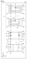
- FIG. 1 is a perspective view of an electronic component according to Embodiment 1;
- FIG. 2 is a cross-sectional view showing the configuration inside the insulator of the electronic component according to Embodiment 1.
- FIG. 2 is an exploded plan view showing the configuration of the electronic component according to Embodiment 1;
- FIG. 3A and 3B are a cross-sectional view and an equivalent circuit diagram showing electrical connection of first external electrodes of the electronic component according to Embodiment 1;
- FIG. 3A and 3B are a cross-sectional view and an equivalent circuit diagram showing electrical connection of first external electrodes of the electronic component according to Embodiment 1;
- FIG. 4A and 4B are diagrams for explaining magnetic field coupling in the electronic component according to the first embodiment;
- FIG. 4 is a diagram showing a comparison result of inductance values between the electronic component according to Embodiment 1 and the electronic component according to a comparative example; 8A and 8B are a cross-sectional view and an equivalent circuit diagram showing the configuration inside the insulator of the electronic component according to the second embodiment; FIG. 8 is an exploded plan view showing the configuration of an electronic component according to Embodiment 2; FIG. 11 is a cross-sectional view showing the configuration inside an insulator of an electronic component according to Embodiment 3; FIG. 11 is an exploded plan view showing the configuration of an electronic component according to Embodiment 3; 10 is an equivalent circuit diagram of an electronic component according to Embodiment 3; FIG. FIG.
- FIG. 11 is a perspective view of an electronic component according to Embodiment 4;
- FIG. 11 is a cross-sectional view showing the configuration inside an insulator of an electronic component according to Embodiment 4;
- FIG. 11 is an exploded plan view showing the configuration of an electronic component according to Embodiment 4;
- FIG. 11 is an equivalent circuit diagram of an electronic component according to Embodiment 4; It is a figure for demonstrating the positional deviation of the conductor pattern of the electronic component which concerns on a comparative example.
- FIG. 11 is a diagram for explaining misalignment of a conductor pattern of an electronic component according to Embodiment 4;
- FIG. 1 is a perspective view of electronic component 100 according to Embodiment 1.
- the short side direction of the electronic component 100 is the X direction
- the long side direction is the Y direction
- the height direction is the Z direction.
- the electronic component 100 according to Embodiment 1 is a chip component type small coil that includes at least one conductor pattern.
- An electronic component 100 includes a rectangular parallelepiped insulator 10 in which a plurality of insulating substrates (insulator layers) on which at least one conductor pattern is formed are laminated.
- the stacking direction of the insulating substrates is the Z direction, and the direction of the arrow in FIG. 1 indicates the upper layer direction.
- the insulating substrate is made of, for example, an insulating material containing borosilicate glass as a main component, or an insulating resin such as alumina, zirconia, or polyimide resin.
- the interfaces between the insulating substrates may not be clearly defined due to processing such as baking or hardening.
- the insulator 10 has a first main surface 11 , a second main surface 12 facing the first main surface 11 , and a first side surface 21 and a second side surface 22 connecting the first main surface 11 and the second main surface 12 . , a third side 23 and a fourth side 24 .
- the first main surface 11 is positioned below the second main surface 12 in the Z direction.
- the first main surface 11 is a mounting surface to be placed on the mounting board, and when the electronic component 100 is mounted on the mounting board, the first main surface 11 faces the mounting board.
- the first main surface 11 is also referred to as a bottom surface or a back surface
- the second main surface 12 is also referred to as a top surface.
- the first side surface 21 and the second side surface 22 are provided in the longitudinal direction (Y direction) of the insulator 10 .
- the first side surface 21 faces the second side surface 22 .
- the third side surface 23 and the fourth side surface 24 are provided in the short direction (X direction) of the insulator 10 .
- the third side surface 23 faces the fourth side surface 24 .
- the electronic component 100 includes a first external electrode 31 and a second external electrode 32 electrically connected to at least one conductor pattern provided inside the insulator 10 .
- the first external electrode 31 is provided closer to the third side surface 23 than the second external electrode 32 in the longitudinal direction (Y direction) of the insulator 10 .
- the second external electrode 32 is provided closer to the fourth side surface 24 than the first external electrode 31 in the longitudinal direction (Y direction) of the insulator 10 .
- the first external electrode 31 and the second external electrode 32 are not limited to the first main surface 11, which is the bottom surface of the insulator 10, but also the first side surface 21 and the second side surface 21 connecting the first main surface 11 and the second main surface 12.
- An electrode (for example, an electrode surface) is also formed on the side surface 22 .
- the first external electrode 31 includes a first electrode 31a provided along the first main surface 11, a second electrode 31b provided along the first side surface 21, and a second electrode 31b provided along the first side surface 22. and a third electrode 31c provided along.
- the second electrode 31b and the third electrode 31c are electrically connected to the first electrode 31a through a path along the outer circumference of the insulator 10.
- the first electrode 31a, the second electrode 31b, and the third electrode 31c are designed to be at the same potential by being electrically connected through a path along the outer periphery of the insulator 10.
- the first external electrode 31 does not have electrodes along the second main surface 12 , the third side surface 23 and the fourth side surface 24 . That is, when the first external electrode 31 is viewed from the third side surface 23 side with the first main surface 11 facing downward (mounting substrate side), the first external electrode 31 is concave (U-shaped) or substantially concave ( approximately U-shaped). Strictly speaking, the end portion 310b of the second electrode 31b provided along the first side surface 21 and the end portion 310c of the third electrode 31c provided along the second side surface 22 hang on the second main surface 12. However, the conductor patterns in the insulator 10 are not directly connected to the ends 310b and 310c. Note that the first external electrode 31 may be provided on the insulator 10 so that the ends 310b and 310c do not overlap the second main surface 12 .
- the second external electrode 32 includes a fourth electrode 32a provided along the first main surface 11, a fifth electrode 32b provided along the first side surface 21, and a fourth electrode 32b provided along the second side surface 22. and a sixth electrode 32c.
- the fifth electrode 32b and the sixth electrode 32c are electrically connected to the fourth electrode 32a through a path along the outer periphery of the insulator 10. As shown in FIG. That is, the fourth electrode 32a, the fifth electrode 32b, and the sixth electrode 32c are electrically connected by a path along the outer circumference of the insulator 10, and thus have the same potential.
- the second external electrode 32 does not have electrodes along the second main surface 12 , the third side surface 23 and the fourth side surface 24 . That is, when the second external electrode 32 is viewed from the fourth side surface 24 side with the first main surface 11 facing downward (mounting substrate side), the second external electrode 32 is concave (U-shaped) or substantially concave ( approximately U-shaped). Strictly speaking, the end portion 320b of the fifth electrode 32b provided along the first side surface 21 and the end portion 320c of the sixth electrode 32c provided along the second side surface 22 hang on the second main surface 12. However, the conductor patterns in the insulator 10 are not directly connected to the ends 320b and 320c. The second external electrode 32 may be provided on the insulator 10 so that the ends 320 b and 320 c do not overlap the second main surface 12 .
- first external electrode 31 and the second external electrode 32 have electrodes on both the first side surface 21 and the second side surface 22
- first external electrode 31 and the second external electrode 32 have electrodes on the first side surface 21 and the second external electrode 32
- second side surface 22 may have an electrode. That is, the first external electrode 31 and the second external electrode 32 are L-shaped when viewed from the third side surface 23 side or the fourth side surface 24 side with the first main surface 11 facing downward (mounting substrate side). Alternatively, it may have a substantially L-shaped shape.
- first external electrode 31 and the second external electrode 32 may have electrodes on the third side surface 23 and the fourth side surface 24 .
- FIG. 2 is a cross-sectional view showing the configuration inside insulator 10 of electronic component 100 according to the first embodiment.
- FIG. 3 is an exploded plan view showing the configuration of electronic component 100 according to the first embodiment.
- the electronic component 100 includes an inductor L1 formed by conductor patterns K1 and K2 inside the insulator 10.
- the conductor pattern K2 is an example of the "first conductor pattern" of the present disclosure.
- the conductor patterns K1 and K2 of the inductor L1 are stacked parallel to the first main surface 11 of the insulator 10 and electrically connected by the via conductors V1.
- the electronic component 100 includes insulating substrates N1 to N3 in order from the second main surface 12 side.
- conductor patterns and electrode patterns are formed by a printing method on the insulating substrates N1 to N3.
- a conductor pattern K1 forming part of the inductor L1 is formed on the insulating substrate N1.
- the conductor pattern K1 is formed so as to make about one turn counterclockwise from the upper left side of the insulating substrate N1 in the figure.
- a starting end of the conductor pattern K1 is electrically connected to the second electrode 31b of the first external electrode 31 .
- a connection portion P1 connected to the via conductor V1 is provided in the vicinity of the terminal end of the conductor pattern K1.
- a conductor pattern K2 forming part of the inductor L1 is formed on the insulating substrate N2.
- the conductor pattern K2 is formed so as to make about one turn counterclockwise from the center of the upper side of the insulating substrate N2 in the figure.
- a connection portion P2 connected to the via conductor V1 is provided in the vicinity of the starting end of the conductor pattern K2.
- a terminal end of the conductor pattern K2 is electrically connected to the fifth electrode 32b of the second external electrode 32. As shown in FIG.
- the inductor L1 forms a coil by connecting the conductor pattern K1 and the conductor pattern K2 in series.
- the inductor L1 is not limited to forming a coil with two conductor patterns, the conductor pattern K1 and the conductor pattern K2, and may form a coil with three or more conductor patterns.
- the conductor patterns K1 and K2 are connected to the second electrode 31b of the first external electrode 31 and the fifth electrode 32b of the second external electrode 32 through the via conductors V1 and V2. is electrically connected to
- the conductor pattern of the inductor is formed over multiple layers, if only the first electrode 31a or the fourth electrode 32a on the first main surface 11 is used, via conductors must be provided over multiple layers, and the inductor L1 or to increase the size of the electronic component while keeping the opening of the inductor L1 as it is.
- the conductor pattern of the inductor can also be formed on the first side surface 21 and the second side surface 22 without using vias. can be connected. Thereby, in electronic component 100 , a conductor pattern can be formed all over the outer frame of insulator 10 .
- the conductor pattern of the inductor can be connected to two locations on the side surfaces.
- the side electrodes By forming the side electrodes in this way, it becomes easier to adjust the length of the conductor pattern, and the degree of freedom in designing the conductor pattern can be improved.
- the second electrode 31b and the third electrode 31c are electrically connected to the first electrode 31a through the path along the outer circumference of the insulator 10. If the electrical connection with the electrode 31b or the third electrode 31c is broken due to a problem, there is a possibility that problems such as a large change in the electrical characteristics of the electronic component 100 may occur.
- the electronic component 100 according to Embodiment 1 further includes an internal conductor SL1 provided inside the insulator 10 and electrically connecting the first electrode 31a and the second electrode 31b.
- the internal conductor SL1 is a bypass conductor that connects the first electrode 31a and the second electrode 31b, but it may be configured to electrically connect the first electrode 31a and the second electrode 31b.
- internal conductor SL1 need not be a bypass conductor.
- the electronic component 100 according to Embodiment 1 further includes an internal conductor SL2 provided inside the insulator 10 and electrically connecting the fourth electrode 32a and the fifth electrode 32b.
- the internal conductor SL2 is a bypass conductor that connects the fourth electrode 32a and the fifth electrode 32b, but it may be configured to electrically connect the fourth electrode 32a and the fifth electrode 32b.
- internal conductor SL2 need not be a bypass conductor.
- the internal conductor SL1 will be mainly described below with reference to FIGS. 4 and 5 in addition to FIG. 3, but the internal conductor SL2 also has the same function as the internal conductor SL1.
- FIG. 4 and 5 are a cross-sectional view and an equivalent circuit diagram showing electrical connections of the first external electrodes 31 of the electronic component 100 according to Embodiment 1.
- FIG. 4 and 5 are views of the A-A' section of the electronic component 100 shown in FIG. 3 as viewed in the Y direction from the third side surface 23 side.
- the internal conductor SL1 is formed on the insulating substrate N3. In the vicinity of the second electrode 31b and the third electrode 31c on the side of the third side surface 23, the internal conductor SL1 extends from substantially the center of the short side direction (X direction) of the insulating substrate N3 to the second electrode 31b. formed. In addition, the internal conductor SL1 extends in the same direction (X direction) as part of the conductor pattern K2 of the inductor L1. When the internal conductor SL1 is viewed in plan from the second main surface 12 side, the internal conductor SL1 is provided at a position overlapping with a part of the conductor pattern K2 in the stacking direction (Z direction).
- the internal conductor SL1 is electrically connected to the second electrode 31b.
- the internal conductor SL1 is provided with a connection portion P6 that is connected to the via conductor V3.
- a connection portion P6 of the internal conductor SL1 is connected to a connection portion P7 provided in the first electrode 31a by a via conductor V3.
- first electrode 31a and the second electrode 31b are electrically connected by a first route passing through the outer circumference of the insulator 10 (that is, a route along the first main surface 11 and the first side surface 21). In addition, they are electrically connected through a second path passing through the via conductor V3 and the internal conductor SL1 in the insulator 10 as well.
- the internal conductor SL2 is formed on the insulating substrate N3. In the vicinity of the fifth electrode 32b and the sixth electrode 32c on the side of the fourth side surface 24, the internal conductor SL2 extends from substantially the center of the short side direction (X direction) of the insulating substrate N3 to the fifth electrode 32b. formed. In addition, the internal conductor SL2 extends in the same direction (X direction) as part of the conductor pattern K2 of the inductor L1. When the internal conductor SL2 is viewed from above from the second main surface 12 side, the internal conductor SL2 is provided at a position overlapping with a part of the conductor pattern K2 in the stacking direction (Z direction).
- the internal conductor SL2 is electrically connected to the fifth electrode 32b.
- the internal conductor SL2 is provided with a connection portion P4 that is connected to the via conductor V2.
- a connection portion P4 of the internal conductor SL2 is connected to a connection portion P5 provided in the fourth electrode 32a by a via conductor V2.
- the fourth electrode 32a and the fifth electrode 32b are electrically connected by the first route passing through the outer circumference of the insulator 10 (that is, the route along the first main surface 11 and the first side surface 21). In addition, they are electrically connected through a second path passing through the via conductor V2 and the internal conductor SL2 in the insulator 10 as well.
- a current IL flows through the conductor pattern K2.
- current IS1 flows along the outer periphery from first electrode 31a to second electrode 31b.
- current IS2 flows from first electrode 31a to second electrode 31b via via conductor V3 and internal conductor SL1.
- the current IS2 flowing through the internal conductor SL1 is parallel and opposite to the current IL flowing through the portion of the conductor pattern K2 that is close to the internal conductor SL1.
- the internal conductor SL1 is magnetically coupled (depolarized) with the conductor pattern K2 such that the polarity of the internal conductor SL1 and the polarity of the conductor pattern K2 are opposite to each other.
- the current IS1' flows along the outer periphery from the fifth electrode 32b to the fourth electrode 32a.
- current IS2' flows from fifth electrode 32b to fourth electrode 32a via internal conductor SL2 and via conductor V2.
- the current IS2′ flowing through the internal conductor SL2 is parallel and opposite to the current IL flowing through the portion of the conductor pattern K2 that is close to the internal conductor SL2. k).
- the internal conductor SL2 is magnetically coupled (depolarized) with the conductor pattern K2 such that the polarity of the internal conductor SL2 and the polarity of the conductor pattern K2 are opposite to each other.
- the electronic component 100 includes a first terminal T1 corresponding to the connection point of the first external electrode 31 on the mounting board and a second terminal T1 corresponding to the connection point of the second external electrode 32 on the mounting board. It includes two terminals T2 and an inductor L1 located between the first terminal T1 and the second terminal T2. The inductor L1 is connected to the second terminal T2.
- Electronic component 100 also includes a parasitic inductance ESL1 and a parasitic inductance ESL2 connected in parallel between first terminal T1 and inductor L1.
- a parasitic inductance ESL1 occurs in the first electrode 31a and the second electrode 31b through which the current IS1 flows.
- a parasitic inductance ESL2 occurs in the internal conductor SL1 through which the current IS2 flows.
- FIG. 6 is a diagram for explaining magnetic field coupling in electronic component 100 according to the first embodiment.
- a magnetic field ML is generated by the current IL in the conductor pattern K2.
- a magnetic field MS is generated by a current IS2 flowing in parallel and in the opposite direction to the current IL.
- Mutual inductance M is generated between the conductor pattern K2 and the internal conductor SL1 by magnetic field coupling between the magnetic field ML generated in the conductor pattern K2 and the magnetic field MS generated in the internal conductor SL1.
- FIG. 6 is a diagram for explaining magnetic field coupling in electronic component 100 according to the first embodiment.
- a magnetic field ML is generated by the current IL in the conductor pattern K2.
- a magnetic field MS is generated by a current IS2 flowing in parallel and in the opposite direction to the current IL.
- Mutual inductance M is generated between the conductor pattern K2 and the internal conductor SL1 by magnetic field coupling between the magnetic field ML generated in the conductor pattern K2 and the magnetic field
- a mutual inductance ⁇ M is set to each of the conductor pattern K2 and the internal conductor SL1 between the parasitic inductance ESL1 and the inductor L1 and parasitic inductance ESL2.
- An equivalent circuit diagram is shown with the addition of inductance +M.
- the first electrode 31a and the second electrode 31b are electrically connected by the first path passing through the outer periphery of the insulator 10, and in addition, the inner portion of the insulator 10 They are electrically connected by a second path passing through conductor SL1.
- the inner conductor inside the insulator 10 Since the electrical connection between the first electrode 31a and the second electrode 31b is maintained on the second path passing through SL1, it is possible to suppress changes in electrical characteristics due to disconnection of the first external electrode 31.
- FIG. 7 is a diagram showing a comparison result of inductance values between the electronic component 100 according to the first embodiment and the electronic component according to the comparative example.
- FIG. 7 shows characteristic changes when the electronic component 100 according to Embodiment 1 is used as an electronic component according to an example, and electronic component 100 according to Embodiment 1 as an electronic component according to a comparative example. It shows the change in characteristics when using an electronic component that has an internal conductor SL1 but is not magnetically coupled.
- the inner conductor SL1 is focused on and the parasitic inductances are compared, but the inner conductor SL2 also has the same effect as the inner conductor SL1.
- the change in inductance value in the portion between the first terminal T1 and the inductor L1 (ESL portion S indicated by broken lines in FIGS. 4B and 5B) is shown.
- the parasitic inductance ESL1 and the parasitic inductance ESL2 are set to 0.5 nH
- the mutual inductance M is set to 0.1 nH.
- the inductance value of the ESL portion S when the first electrode 31a and the second electrode 31b are electrically connected on the first path passing through the outer periphery of the insulator 10 is While the inductance value is 0.24 nH, the inductance value of the ESL portion S when the first electrode 31a and the second electrode 31b are disconnected is 0.40 nH, and the amount of change is 0.16 nH.
- the inductance value of the ESL portion S is 0.25 nH when the first electrode 31a and the second electrode 31b are electrically connected in the first path passing through the outer periphery of the insulator 10.
- the inductance value of the ESL portion S when the first electrode 31a and the second electrode 31b are disconnected is 0.50 nH, and the amount of change is 0.25 nH.
- the electronic component 100 according to Embodiment 1 when the electrical connection between the first electrode 31a and the second electrode 31b is cut, the passage path in the ESL portion S is only ESL2, so the inductance value of the ESL portion S is
- the magnetic field coupling (depolarization coupling) between the internal conductor SL1 and the conductor pattern K2 causes the ESL2
- the mutual inductance M increases as the amount of the current IS2 flowing through increases, the amount of increase in the inductance value of the ESL portion S represented by ESL2-M can be suppressed. Therefore, the electronic component 100 corresponding to the example can suppress the amount of change in the inductance value of the ESL portion S more than the comparative example.
- the inner conductor SL1 provided in the insulator 10 keeps the second electrode
- the electrical connection between the first electrode 31a and the second electrode 31b can be maintained, and further, by magnetically coupling the internal conductor SL2 and the conductor pattern K2, according to the increase in the current flowing through the internal conductor SL2 due to the disconnection, , the mutual inductance increases, so that the change in electrical characteristics due to disconnection of the first external electrode 31 can be further suppressed.
- the internal conductor SL1 is not limited to electrically connecting the first electrode 31a and the second electrode 31b. may be provided within
- the internal conductor SL1 does not have to be provided at a position that partially overlaps the conductor pattern K2 when the internal conductor SL1 is viewed from the second main surface 12 side. It is sufficient if it is a position where magnetic field coupling occurs at .
- the current IS2 flowing through the inner conductor SL1 may not be parallel to the current IL flowing through the conductor pattern K2, and the inner conductor SL1 is arranged out of parallel so as to magnetically couple with the conductor pattern K2.
- Embodiment 2 An electronic component 200 according to Embodiment 2 will be described with reference to FIGS. 8 and 9.
- FIG. 2 As electronic component 200, a chip component type compact filter device in which inductor L1 and capacitor C1 are connected in series will be described.
- the electronic component 200 according to Embodiment 2 only the configuration different from that of the electronic component 100 according to Embodiment 1 will be mainly described.
- the electronic component 200 according to No. 2 is also given the same reference numerals, and the description thereof is omitted.
- FIG. 8 is a cross-sectional view and an equivalent circuit diagram showing the configuration inside insulator 10 of electronic component 200 according to the second embodiment.
- FIG. 9 is an exploded plan view showing the configuration of electronic component 200 according to the second embodiment.
- electronic component 200 includes, within insulator 10, an inductor L1 configured by conductor patterns K1 and K2, and a capacitor C1 configured by electrode patterns K3 and K4. By connecting inductor L1 and capacitor C1 in series within insulator 10, electronic component 200 forms a series resonance circuit.
- the conductor pattern K2 is an example of the "first conductor pattern" of the present disclosure.
- the electrode patterns K3 and K4 of the capacitor C1 are stacked below the conductor patterns K1 and K2 of the inductor L1 in the Z direction via an insulating layer. That is, the capacitor C1 is arranged closer to the first main surface 11 than the inductor L1. When the capacitor C1 is viewed from the second main surface 12 side, the electrode patterns K3 and K4 of the capacitor C1 are provided at positions that partially overlap the conductor patterns K1 and K2 in the stacking direction (Z direction).
- the electronic component 200 further includes an insulating substrate N4 between the insulating substrates N2 and N3.
- An electrode pattern K4 forming one electrode of the capacitor C1 is formed on the insulating substrate N4.
- the electrode pattern K4 is provided at a position overlapping part of the conductor patterns K1 and K2 in the stacking direction (Z direction). That is, the electrode pattern K4 is provided at a position that reduces the area overlapping the opening of the inductor L1 formed by the conductor patterns K1 and K2.
- the electrode pattern K4 is provided with a connection portion P8 that is connected to the via conductor V4. That is, the electrode pattern K4 is connected to the connecting portion P3 of the conductor pattern K2 of the inductor L1 by the via conductor V4.
- An electrode pattern K3 forming the other electrode of the capacitor C1 is formed on the insulating substrate N3.
- the electrode pattern K3 is provided at a position overlapping part of the conductor patterns K1 and K2 in the stacking direction (Z direction). That is, the electrode pattern K3 is provided at a position that reduces the area overlapping the opening of the inductor L1 formed by the conductor patterns K1 and K2.
- a connection portion P4 of the electrode pattern K3 is connected to a connection portion P5 provided in the fourth electrode 32a by a via conductor V2.
- the electrode pattern K3 is electrically connected to the sixth electrode 32c of the second external electrode 32.
- the path leading from connection portion P5 provided in fourth electrode 32a to sixth electrode 32c of second external electrode 32 via via conductor V2 and electrode pattern K3 corresponds to the fourth electrode 32c of electronic component 100 according to the first embodiment. It corresponds to a path leading from the connection portion P5 provided in the electrode 32a to the fifth electrode 32b of the second external electrode 32 via the via conductor V2 and the internal conductor SL2.
- the insulator 10 can be used not only in a small chip component type coil including the inductor L1, but also in a small chip component type filter device forming a resonance circuit such as the electronic component 200 according to the second embodiment.
- the first electrode 31a and the second electrode 31b may be electrically connected by an internal conductor SL1 provided therein.
- the internal conductor SL1 is formed on the same insulating substrate N3 as the electrode pattern K3 forming the capacitor C1.
- the internal conductor SL1 is provided at a position overlapping part of the conductor pattern K2 in the lamination direction (Z direction), and extends in the same direction (X direction) as part of the conductor pattern K2 of the inductor L1.
- the current flowing through the internal conductor SL1 is parallel and opposite to the current flowing through the portion of the conductor pattern K2 that is adjacent to the internal conductor SL1, and the internal conductor SL1 and the conductor pattern K2 are magnetically coupled (depolarized) to each other. are doing.
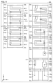
- FIG. 3 An electronic component 300 according to Embodiment 3 will be described with reference to FIGS. 10 to 12.
- FIG. In the third embodiment, as electronic component 300, a small chip component type filter device in which inductor L12 and capacitor C11 are connected in series and inductor L12, capacitor C11 and inductor L11 are connected in parallel will be described. .
- electronic component 300 according to Embodiment 3 only the configuration different from electronic component 100 according to Embodiment 1 and electronic component 200 according to Embodiment 2 will be mainly described.
- the same components as those of the component 100 and the electronic component 200 according to the second embodiment are denoted by the same reference numerals, and descriptions thereof are omitted.
- FIG. 10 is a cross-sectional view showing the configuration inside the insulator 10 of the electronic component 300 according to the third embodiment.
- FIG. 11 is an exploded plan view showing the configuration of electronic component 300 according to the third embodiment.
- electronic component 300 includes, in insulator 10, inductor L11 formed of conductor patterns K11 to K14, inductor L12 formed of conductor patterns K15 to K18, and electrode pattern K19. , K20.
- inductor L12 and capacitor C11 are connected in series, and inductor L12, capacitor C11, and inductor L11 are connected in parallel, whereby electronic component 300 forms a resonance circuit.
- the conductor pattern K18 is an example of the "first conductor pattern” of the present disclosure.
- the inductor L12 is an example of the “inductor” of the present disclosure, and the inductor L11 is an example of the "other inductor” of the present disclosure.
- the conductor patterns K11 to K14 of the inductor L11 are stacked parallel to the first main surface 11 of the insulator 10 and electrically connected by a plurality of via conductors.
- the conductor patterns K15 to K18 of the inductor L12 are stacked parallel to the first main surface 11 of the insulator 10 and electrically connected by a plurality of via conductors.
- the inductor L11 is arranged closer to the second main surface 12 than the inductor L12.
- the conductor patterns K15 to K18 of the inductor L12 are stacked below the conductor patterns K11 to K14 of the inductor L11 in the Z direction via an insulating layer. That is, the inductor L12 is arranged closer to the first main surface 11 than the inductor L11.
- the electrode patterns K19 and K20 of the capacitor C11 are stacked below the conductor patterns K15 to K18 of the inductor L12 in the Z direction via an insulating layer. That is, the capacitor C11 is arranged closer to the first main surface 11 than the inductors L11 and L12.
- the electronic component 300 includes insulating substrates N1 to N20 in order from the second main surface 12 side.
- conductor patterns and electrode patterns are formed by a printing method on the insulating substrates N1 to N20.
- a conductor pattern K11 forming part of the inductor L11 is formed on the insulating substrate N11.
- the conductor pattern K11 is formed so as to extend clockwise about 3/4 from the upper left side of the insulating substrate N11 in the figure.
- the starting end of the conductor pattern K11 is electrically connected to the second electrode 31b of the first external electrode 31.
- a connection portion P11 connected to the via conductor V11A and a connection portion P12 connected to the via conductor V11B are provided in the vicinity of the terminal end of the conductor pattern K11.
- a conductor pattern K12 forming part of the inductor L11 is formed on the insulating substrate N12.
- the conductor pattern K12 is formed so as to extend clockwise about 3/4 from the upper left side of the insulating substrate N12 in the drawing.
- the starting end of the conductor pattern K12 is electrically connected to the second electrode 31b of the first external electrode 31.
- a connection portion P13 connected to the via conductors V11A and V12A and a connection portion P14 connected to the via conductors V11B and V12B are provided near the end of the conductor pattern K12.
- a conductor pattern K13 forming part of the inductor L11 is formed on the insulating substrate N13.
- the conductor pattern K13 is formed so as to extend about 3/4 clockwise from the lower right side of the insulating substrate N13 in the figure.
- a connection portion P15 connected to the via conductors V12A and V13A and a connection portion P15 connected to the via conductors V12B and V13B are provided in the vicinity of the starting end of the conductor pattern K13.
- a terminal end of the conductor pattern K13 is electrically connected to the fifth electrode 32b of the second external electrode 32. As shown in FIG.
- a conductor pattern K14 forming part of the inductor L11 is formed on the insulating substrate N14.
- the conductor pattern K14 is formed so as to extend clockwise about 3/4 from the lower right side of the insulating substrate N14 in the figure.
- a connection portion P17 connected to the via conductor V13A and a connection portion P18 connected to the via conductor V13B are provided in the vicinity of the starting end of the conductor pattern K14.
- a terminal end of the conductor pattern K14 is electrically connected to the fifth electrode 32b of the second external electrode 32. As shown in FIG.
- the inductor L11 has the conductor patterns K11 and K12 connected in parallel, the conductor patterns K13 and K14 connected in parallel, and the conductor patterns K11, K12 and the conductor patterns K13, K14 connected in series.
- a coil is formed by being connected.
- a conductor pattern K15 forming part of the inductor L12 is formed on the insulating substrate N15.
- the conductor pattern K15 is formed so as to make about one turn counterclockwise from the upper left side of the insulating substrate N15 in the figure.
- the starting end of the conductor pattern K15 is electrically connected to the second electrode 31b of the first external electrode 31.
- a connection portion P19 connected to the via conductor V14 is provided in the vicinity of the terminal end of the conductor pattern K15.
- a conductor pattern K16 forming part of the inductor L12 is formed on the insulating substrate N16.
- the conductor pattern K16 is formed so as to make about one turn counterclockwise from the upper left side of the insulating substrate N16 in the figure.
- the starting end of the conductor pattern K16 is electrically connected to the second electrode 31b of the first external electrode 31.
- a connection portion P20 connected to the via conductors V14 and V15 is provided near the end of the conductor pattern K16.
- a conductor pattern K17 forming part of the inductor L12 is formed on the insulating substrate N17.
- the conductor pattern K17 is formed so as to make about one turn counterclockwise from the upper side of the insulating substrate N17 in the figure.
- a connection portion P21 connected to the via conductors V15 and V16A is provided in the vicinity of the starting end of the conductor pattern K17.
- a connection portion P22 connected to the via conductor V16B is provided in the vicinity of the terminal end of the conductor pattern K17.
- a conductor pattern K18 forming part of the inductor L12 is formed on the insulating substrate N18.
- the conductor pattern K18 is formed so as to make about one turn counterclockwise from the upper side of the insulating substrate N18 in the figure.
- a connection portion P23 connected to the via conductor V16A is provided in the vicinity of the starting end of the conductor pattern K18.
- a connection portion P24 connected to the via conductors V16B and V17 is provided near the end of the conductor pattern K18.
- the inductor L12 has the conductor patterns K15 and K16 connected in parallel, the conductor patterns K17 and K18 connected in parallel, and the conductor patterns K15, K16 and the conductor patterns K17, K18 connected in series.
- a coil is formed by being connected.
- An electrode pattern K19 forming one electrode of the capacitor C11 is formed on the insulating substrate N19.
- the electrode pattern K19 is provided at a position overlapping part of the conductor patterns K17 and K18 in the stacking direction (Z direction). That is, the electrode pattern K19 is provided at a position that reduces the area overlapping the opening of the inductor L12 formed by the conductor patterns K17 and K18.
- the electrode pattern K19 is provided with a connection portion P25 that connects to the via conductor V17. That is, the electrode pattern K19 is connected to the connection portion P24 of the conductor pattern K18 of the inductor L12 by the via conductor V17.
- An electrode pattern K20 forming the other electrode of the capacitor C11 is formed on the insulating substrate N20.
- the electrode pattern K20 is provided at a position overlapping part of the conductor patterns K17 and K18 in the stacking direction (Z direction). That is, the electrode pattern K20 is provided at a position that reduces the area overlapping the opening of the inductor L11 formed by the conductor patterns K17 and K18.
- the electrode pattern K20 is provided with a connection portion P26 that is connected to the via conductor V18.
- a connection portion P26 of the electrode pattern K20 is connected to a connection portion P28 provided in the fourth electrode 32a by a via conductor V18.
- the electrode pattern K20 is electrically connected to the fifth electrode 32b and the sixth electrode 32c of the second external electrode 32. As shown in FIG.
- the internal conductor SL1 provided in the insulator 10 allows the first electrode 31a and the second electrode 31a to be connected to each other.
- the two electrodes 31b may be electrically connected.
- the internal conductor SL1 is formed on the same insulating substrate N20 as the electrode pattern K20 forming the capacitor C11.
- the internal conductor SL1 is provided at a position overlapping part of the conductor pattern K18 in the lamination direction (Z direction), and extends in the same direction (X direction) as part of the conductor pattern K18 of the inductor L12.
- the current flowing through the internal conductor SL1 is parallel and opposite to the current flowing through the portion of the conductor pattern K18 that is adjacent to the internal conductor SL1, and the internal conductor SL1 and the conductor pattern K18 are magnetically coupled (depolarized) to each other. are doing.
- FIG. 12 is an equivalent circuit diagram of the electronic component according to the third embodiment.
- an electronic component 300 according to Embodiment 3 includes a first terminal T1, an ESL section S connected to the first terminal T1, an inductor L12 connected to the ESL section S, and an inductor L12 and a second terminal T2 connected to the capacitor C11.
- electronic component 300 includes an inductor L11 connected in parallel with inductor L12 and capacitor C11.
- the ESL section S includes a parasitic inductance ESL1 and a parasitic inductance ESL2 connected in parallel.
- the first terminal T1 corresponds to the connection point of the first external electrode 31 on the mounting substrate
- the second terminal T2 corresponds to the connection point of the second external electrode 32 on the mounting substrate.
- the inductor L11 and the inductor L12 are magnetically coupled to each other. Also, the conductor pattern K18 of the inductor L12 and the internal conductor SL1 are magnetically coupled to each other.
- the first electrode 31a and the second electrode 31b being electrically connected through the first path passing through the outer circumference of the insulator 10, They are electrically connected by a second path passing through internal conductor SL1 in insulator 10 .
- the first electrode 31a and the second electrode Even if the electrical connection with 31b is cut off, the electrical connection between the first electrode 31a and the second electrode 31b is maintained through the second path passing through the internal conductor SL1 in the insulator 10. It is possible to suppress a change in electrical characteristics due to disconnection of the 1 external electrode 31 .
- FIG. 4 An electronic component 400 according to Embodiment 4 will be described with reference to FIGS. 13 to 18.
- the electronic component 400 according to the fourth embodiment has the same configuration as the electronic component 100 according to the first embodiment, the electronic component 200 according to the second embodiment, and the electronic component 300 according to the third embodiment. While attaching the same reference numerals, the description thereof will be omitted.
- FIG. 13 is a perspective view of electronic component 400 according to Embodiment 4.
- FIG. 13 Note that the first external electrode 31 and the second external electrode 32 included in the electronic component 400 according to the fourth embodiment shown in FIG. 13 and the first external electrode 31 included in the electronic component 100 according to the first embodiment shown in FIG. and the second external electrodes 32 are arranged in symmetrical positions in the Y direction.
- the first external electrode 31 is provided closer to the fourth side surface 24 than the second external electrode 32 in the longitudinal direction (Y direction) of the insulator 10 .
- the second external electrode 32 is provided closer to the third side surface 23 than the first external electrode 31 in the longitudinal direction (Y direction) of the insulator 10 .
- the first external electrode 31 includes a first electrode 31a provided along the first main surface 11, a second electrode 31b provided along the first side surface 21, and a second electrode 31b provided along the second side surface 22. and a third electrode 31c.
- the second external electrode 32 includes a fourth electrode 32a provided along the first main surface 11, a fifth electrode 32b provided along the first side surface 21, and a fourth electrode 32b provided along the second side surface 22. and a sixth electrode 32c.
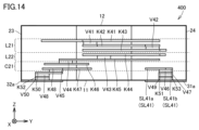
- FIG. 14 is a cross-sectional view showing the configuration inside insulator 10 of electronic component 400 according to the fourth embodiment.
- FIG. 15 is an exploded plan view showing the configuration of electronic component 400 according to the fourth embodiment.
- electronic component 400 is a chip component type compact filter device in which inductor L22 and capacitor C21 are connected in series, and inductor L22, capacitor C21, and inductor L21 are connected in parallel. is.
- electronic component 400 includes, in insulator 10, an inductor L21 configured by conductor patterns K41 to K43, an inductor L22 configured by conductor patterns K44 and K45, and electrode patterns K46 and K47. and a capacitor C21.
- Inductor L22 and capacitor C21 are connected in series within insulator 10, and inductor L22, capacitor C21, and inductor L21 are connected in parallel, whereby electronic component 400 forms a resonance circuit.
- the conductor pattern K45 is an example of the "first conductor pattern" of the present disclosure.
- the inductor L22 is an example of the "inductor” of the present disclosure
- the inductor L21 is an example of the "other inductor” of the present disclosure.
- the conductor patterns K41 to K43 of the inductor L21 are stacked parallel to the first main surface 11 of the insulator 10 and electrically connected by a plurality of via conductors.
- the conductor patterns K44, K45 of the inductor L22 are stacked parallel to the first main surface 11 of the insulator 10 and electrically connected by a plurality of via conductors.
- the inductor L21 is arranged closer to the second main surface 12 than the inductor L22.
- the conductor patterns K44 and K45 of the inductor L22 are stacked below the conductor patterns K41 to K43 of the inductor L21 in the Z direction via an insulating layer. That is, the inductor L22 is arranged closer to the first main surface 11 than the inductor L21.
- the electrode patterns K46 and K47 of the capacitor C21 are stacked below the conductor patterns K44 and K45 of the inductor L22 in the Z direction via an insulating layer. That is, the capacitor C21 is arranged closer to the first main surface 11 than the inductors L21 and L22.
- the electronic component 400 includes insulating substrates N41 to N49 in order from the second main surface 12 side.
- conductor patterns and electrode patterns are formed on insulating substrates N41 to N49 by a printing method.
- a conductor pattern K41 forming part of the inductor L21 is formed on the insulating substrate N41.
- the conductor pattern K41 is formed so as to extend clockwise about 3/4 from the upper left side of the insulating substrate N41 in the drawing.
- the starting end of the conductor pattern K41 is electrically connected to the fifth electrode 32b of the second external electrode 32.
- a connection portion P41 connected to the via conductor V41 is provided in the vicinity of the terminal end of the conductor pattern K41.
- a conductor pattern K42 forming part of the inductor L21 is formed on the insulating substrate N42.
- the conductor pattern K42 is formed so as to extend clockwise about 3/4 from the lower left side of the insulating substrate N42 in the figure.
- a connection portion P42 connected to the via conductor V41 is provided in the vicinity of the starting end of the conductor pattern K42.
- a connection portion P43 connected to the via conductor V42 is provided in the vicinity of the terminal end of the conductor pattern K42.
- a conductor pattern K43 forming part of the inductor L21 is formed on the insulating substrate N43.
- the conductor pattern K43 is formed so as to extend counterclockwise about 3/4 from the lower right side of the insulating substrate N43 in the figure.
- a connection portion P44 connected to the via conductor V42 is provided in the vicinity of the starting end of the conductor pattern K43.
- a terminal end of the conductor pattern K43 is electrically connected to the second electrode 31b of the second external electrode 32 .
- the inductor L21 forms a coil by connecting the conductor pattern K41, the conductor pattern K42, and the conductor pattern K43 in series.
- a conductor pattern K44 forming part of the inductor L22 is formed on the insulating substrate N44.
- the conductor pattern K44 is formed so as to extend clockwise about 3/4 from the upper right side of the insulating substrate N44 in the figure.
- the starting end of the conductor pattern K44 is electrically connected to the second electrode 31b of the first external electrode 31.
- a connection portion P45 connected to the via conductor V43 is provided in the vicinity of the terminal end of the conductor pattern K44.
- a conductor pattern K45 forming part of the inductor L22 is formed on the insulating substrate N45.
- the conductor pattern K45 is formed so as to extend clockwise about 3/4 from the upper side of the insulating substrate N45 in the figure.
- the conductor pattern K45 includes a linear conductor pattern K45a that is straight between the second electrode 31b and the third electrode 31c.
- a connection portion P46 connected to the via conductor V43 is provided in the vicinity of the starting end of the conductor pattern K45.
- a connection portion P47 connected to the via conductor V44 is provided in the vicinity of the terminal end of the conductor pattern K45.
- the inductor L22 forms a coil by connecting the conductor pattern K44 and the conductor pattern K45 in series.
- An electrode pattern K46 forming one electrode of the capacitor C21 is formed on the insulating substrate N46.
- the electrode pattern K46 is provided at a position that reduces the area overlapping the openings of the inductors L21 and L22 in the stacking direction (Z direction).
- a compact filter device (electronic component 400) can be realized without interfering with the magnetic field generated by inductors L21 and L22.
- the electrode pattern K46 is provided with a connection portion P48 that is connected to the via conductor V44. That is, the electrode pattern K46 is connected to the connection portion P47 of the conductor pattern K45 of the inductor L22 by the via conductor V44.
- An electrode pattern K47 forming the other electrode of the capacitor C21 is formed on the insulating substrate N47.
- the electrode pattern K47 is planarly viewed from the second main surface 12 side, the electrode pattern K47 is provided at a position overlapping the electrode pattern K46 in the stacking direction (Z direction).
- the electrode pattern K47 is provided with a connection portion P49 that is connected to the via conductor V45.
- the electrode pattern K47 is electrically connected to the fifth electrode 32b and the sixth electrode 32c of the second external electrode 32 via the wiring pattern K48.
- the wiring pattern K48 is not limited to one wiring that overlaps with the electrode pattern K47, and may be composed of a plurality of wiring patterns.
- an internal conductor SL41 is formed on the same insulating substrate N47 as the electrode pattern K47 that constitutes the capacitor C21.
- Internal conductor SL41 includes internal conductor SL41a and internal conductor SL41b.
- the internal conductor SL41a and the internal conductor SL41b are electrically connected by partially overlapping each other.
- a connection portion P50 connected to the via conductor V46 is provided in the internal conductor SL41b.
- the internal conductor SL41a includes a linear conductor portion that connects the second electrode 31b and the third electrode 31c.
- the straight conductor portion of the internal conductor SL41a is composed of a single layer of conductor extending in the same direction (X direction) as the straight conductor pattern K45a of the inductor L22.
- the straight conductor portion of the internal conductor SL41a is provided at a position overlapping the straight conductor pattern K45a of the conductor pattern K45.
- the current flowing through the internal conductor SL41 is parallel and opposite to the current flowing through the portion (straight conductor pattern K45a) of the conductor pattern K45 that is adjacent to the internal conductor SL41a.
- K45a) are magnetically coupled (depolarized coupling) with each other.
- a wiring pattern K50 is formed on the insulating substrate N48.
- the wiring pattern K50 is provided at a position overlapping with a part of the electrode pattern K47 in the stacking direction (Z direction).
- the wiring pattern K50 is provided with a connection portion P51 that is connected to the via conductor V45. That is, the wiring pattern K50 is connected to the connection portion P49 of the electrode pattern K47 of the capacitor C21 by the via conductor V45. Further, the wiring pattern K50 is provided with a connection portion P53 that is connected to the via conductor V48.
- a wiring pattern K51 is formed on the insulating substrate N48.
- the wiring pattern K51 is provided at a position overlapping the internal conductor SL41b in the stacking direction (Z direction).
- the wiring pattern K51 is provided with a connection portion P52 that connects to the via conductor V46 and the via conductor V47. That is, the wiring pattern K51 is connected to the connection portion P50 of the internal conductor SL41b by the via conductor V46.
- a wiring pattern K52 is formed on the insulating substrate N49.
- the wiring pattern K52 is provided at a position overlapping with a part of the wiring pattern K50 in the lamination direction (Z direction).
- the wiring pattern K52 is provided with a connection portion P54 that connects to the via conductor V48 and the via conductor V50. That is, the wiring pattern K52 is connected to the connection portion P53 of the wiring pattern K50 by the via conductor V48.
- the wiring pattern K52 is connected to a connection portion P57 provided in the fourth electrode 32a by a via conductor V50.
- a wiring pattern K53 is formed on the insulating substrate N49.
- the wiring pattern K53 is provided at a position overlapping with a part of the wiring pattern K51 in the stacking direction (Z direction).
- the wiring pattern K53 is provided with a connection portion P55 that connects to the via conductor V47 and the via conductor V49. That is, the wiring pattern K53 is connected to the connection portion P52 of the wiring pattern K51 by the via conductor V47.
- the wiring pattern K53 is connected to a connection portion P56 provided in the first electrode 31a by a via conductor V49.
- FIG. 16 is an equivalent circuit diagram of electronic component 400 according to the fourth embodiment.
- an electronic component 400 according to Embodiment 4 includes a first terminal T1, an ESL section S connected to the first terminal T1, an inductor L22 connected to the ESL section S, and an inductor L22 and a second terminal T2 connected to the capacitor C21.
- electronic component 400 includes an inductor L21 connected in parallel with inductor L22 and capacitor C21.
- the ESL section S includes a parasitic inductance ESL1 and a parasitic inductance ESL2 connected in parallel.
- the first terminal T1 corresponds to the connection point of the first external electrode 31 on the mounting substrate
- the second terminal T2 corresponds to the connection point of the second external electrode 32 on the mounting substrate.
- the inductor L21 and the inductor L22 are magnetically coupled to each other. Also, the conductor pattern K45 of the inductor L22 and the internal conductor SL41 are magnetically coupled to each other.
- the internal conductor SL41 is connected to the first electrode 31a provided on the first main surface 11 and the second Although it is connected to the second electrode 31b provided on the first side surface 21, in the electronic component 400, unlike the electronic component 300, the internal conductor SL41 is also connected to the third electrode 31c provided on the second side surface 22. It is connected. Further, the internal conductor SL41 extends in the same direction (X direction) as the conductor pattern K45 of the inductor L22, and when the conductor pattern K45 and the internal conductor SL41 are viewed from the second main surface 12 side, the conductor pattern K45 It is located in a position overlapping with the As shown in FIG.
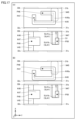
- FIG. 17 is a diagram for explaining misalignment of conductor patterns of an electronic component according to a comparative example.
- the conductor pattern K45 changes from the state shown in FIG. 17(A) to the state shown in FIG. 17(B) in the X direction. If they shift, the area of the portion where the internal conductor SL41 and the straight conductor pattern K45a of the conductor pattern K45 overlap in the stacking direction (Z direction) becomes smaller.
- FIG. 18 is a diagram for explaining the positional deviation of the conductor pattern K45 of the electronic component 400 according to the fourth embodiment.
- the conductor pattern K45 changes from the state shown in FIG. 18(A) to the state shown in FIG. 18(B) in the X direction. Even if there is a shift, the overlapping area of the internal conductor SL41 and the straight conductor pattern K45a of the conductor pattern K45 in the stacking direction (Z direction) is unlikely to change.
- the electronic component 400 can maintain the magnetic field coupling (depolarizing coupling) between the internal conductor SL41 and the conductor pattern K45 without change, so that a change in electrical characteristics due to disconnection of the first external electrode 31 can be reliably prevented. can be reduced to
- the internal conductor SL41 is connected to the second electrode 31b provided on the first side surface 21, and is also connected to the third electrode 31c provided on the second side surface 22. Since it is connected, heat can be released not only to the first side surface 21 but also to the second side surface 22, and heat dissipation can be improved.
- An electronic component includes an insulator, an inductor configured in the insulator and having a first conductor pattern, and an external electrode electrically connected to the first conductor pattern.
- the insulator has a first main surface, a second main surface facing the first main surface, and a first side surface, a second side surface, a third side surface, and a fourth side surface connecting the first main surface and the second main surface. side.
- the first side faces the second side.
- the third side faces the fourth side.
- the external electrode has a first electrode portion provided along the first main surface and a second electrode portion provided along the first side surface.
- the electronic component includes an internal conductor provided in the insulator and electrically connecting the first electrode portion and the second electrode portion.
- the internal conductor has a current flowing through the internal conductor and a portion of the first conductor pattern that is the closest to the internal conductor. It has a portion where the current flows in the opposite direction.
- the external electrode is provided along the second side surface and is electrically connected to the first electrode section. It further has an electrode part.
- the internal conductor further electrically connects the first electrode portion and the third electrode portion.
- the internal conductor is composed of a single layer of conductor that connects the second electrode and the third electrode.
- the internal conductor includes a linear conductor portion that connects the second electrode portion and the third electrode portion.
- the first conductor pattern includes a linear conductor pattern between the second electrode portion and the third electrode portion.
- the straight conductor portion of the internal conductor overlaps the straight conductor pattern of the first conductor pattern when viewed from the second main surface side.
- the first main surface is a surface to be placed on the mounting board.
- the electronic component according to any one of items 1 to 12 further includes a capacitor connected in series with the inductor within the insulator.
- one of the electrode patterns forming the capacitor is formed on the same plane as part of the internal conductor.
- the electronic component according to Item 13 or 14 further includes another inductor connected in parallel with the inductor within the insulator.
Landscapes
- Engineering & Computer Science (AREA)
- Power Engineering (AREA)
- Microelectronics & Electronic Packaging (AREA)
- Manufacturing & Machinery (AREA)
- Coils Or Transformers For Communication (AREA)
Priority Applications (3)
| Application Number | Priority Date | Filing Date | Title |
|---|---|---|---|
| CN202380015362.5A CN118414680A (zh) | 2022-02-04 | 2023-01-24 | 电子部件 |
| JP2023578490A JP7761065B2 (ja) | 2022-02-04 | 2023-01-24 | 電子部品 |
| US18/738,436 US20240347257A1 (en) | 2022-02-04 | 2024-06-10 | Electronic component |
Applications Claiming Priority (4)
| Application Number | Priority Date | Filing Date | Title |
|---|---|---|---|
| JP2022-016417 | 2022-02-04 | ||
| JP2022016417 | 2022-02-04 | ||
| JP2022-076021 | 2022-05-02 | ||
| JP2022076021 | 2022-05-02 |
Related Child Applications (1)
| Application Number | Title | Priority Date | Filing Date |
|---|---|---|---|
| US18/738,436 Continuation US20240347257A1 (en) | 2022-02-04 | 2024-06-10 | Electronic component |
Publications (1)
| Publication Number | Publication Date |
|---|---|
| WO2023149277A1 true WO2023149277A1 (ja) | 2023-08-10 |
Family
ID=87552210
Family Applications (1)
| Application Number | Title | Priority Date | Filing Date |
|---|---|---|---|
| PCT/JP2023/002061 Ceased WO2023149277A1 (ja) | 2022-02-04 | 2023-01-24 | 電子部品 |
Country Status (3)
| Country | Link |
|---|---|
| US (1) | US20240347257A1 (https=) |
| JP (1) | JP7761065B2 (https=) |
| WO (1) | WO2023149277A1 (https=) |
Cited By (1)
| Publication number | Priority date | Publication date | Assignee | Title |
|---|---|---|---|---|
| WO2025052762A1 (ja) * | 2023-09-07 | 2025-03-13 | 株式会社村田製作所 | フィルタ装置、アンテナ装置、およびアンテナモジュール |
Citations (3)
| Publication number | Priority date | Publication date | Assignee | Title |
|---|---|---|---|---|
| WO2012086397A1 (ja) * | 2010-12-21 | 2012-06-28 | 株式会社村田製作所 | 積層コイル部品 |
| JP2020119979A (ja) * | 2019-01-23 | 2020-08-06 | Tdk株式会社 | 積層コイル部品 |
| US20200357565A1 (en) * | 2019-05-07 | 2020-11-12 | Samsung Electro-Mechanics Co., Ltd. | Coil electronic component |
Family Cites Families (3)
| Publication number | Priority date | Publication date | Assignee | Title |
|---|---|---|---|---|
| JPH1167554A (ja) * | 1997-08-26 | 1999-03-09 | Murata Mfg Co Ltd | 積層型コイル部品及びその製造方法 |
| WO2015146814A1 (ja) * | 2014-03-27 | 2015-10-01 | 株式会社村田製作所 | 電子部品 |
| JP6536437B2 (ja) * | 2016-03-04 | 2019-07-03 | 株式会社村田製作所 | 電子部品 |
-
2023
- 2023-01-24 JP JP2023578490A patent/JP7761065B2/ja active Active
- 2023-01-24 WO PCT/JP2023/002061 patent/WO2023149277A1/ja not_active Ceased
-
2024
- 2024-06-10 US US18/738,436 patent/US20240347257A1/en active Pending
Patent Citations (3)
| Publication number | Priority date | Publication date | Assignee | Title |
|---|---|---|---|---|
| WO2012086397A1 (ja) * | 2010-12-21 | 2012-06-28 | 株式会社村田製作所 | 積層コイル部品 |
| JP2020119979A (ja) * | 2019-01-23 | 2020-08-06 | Tdk株式会社 | 積層コイル部品 |
| US20200357565A1 (en) * | 2019-05-07 | 2020-11-12 | Samsung Electro-Mechanics Co., Ltd. | Coil electronic component |
Cited By (1)
| Publication number | Priority date | Publication date | Assignee | Title |
|---|---|---|---|---|
| WO2025052762A1 (ja) * | 2023-09-07 | 2025-03-13 | 株式会社村田製作所 | フィルタ装置、アンテナ装置、およびアンテナモジュール |
Also Published As
| Publication number | Publication date |
|---|---|
| JP7761065B2 (ja) | 2025-10-28 |
| US20240347257A1 (en) | 2024-10-17 |
| JPWO2023149277A1 (https=) | 2023-08-10 |
Similar Documents
| Publication | Publication Date | Title |
|---|---|---|
| KR102460765B1 (ko) | 커먼 모드 노이즈 필터 | |
| US10305441B2 (en) | Common mode noise filter | |
| WO2012033031A1 (ja) | アンテナ装置および通信端末装置 | |
| US10778177B2 (en) | Common mode noise filter | |
| US10748698B2 (en) | Electronic component | |
| JP7761065B2 (ja) | 電子部品 | |
| CN108023152B (zh) | 定向耦合器 | |
| CN115623658A (zh) | 电路板、电子设备和制造电路板的方法 | |
| CN114334351B (zh) | 线圈部件 | |
| CN100583327C (zh) | 噪声滤波器 | |
| US12592336B2 (en) | Laminated common mode filter | |
| CN118414680A (zh) | 电子部件 | |
| US10004144B2 (en) | Connector module | |
| WO2023149240A1 (ja) | 電子部品 | |
| JP5754201B2 (ja) | 積層構造型バラン | |
| JP5545363B2 (ja) | 複合部品 | |
| US20250357908A1 (en) | Electronic component | |
| WO2023149279A1 (ja) | 電子部品 | |
| US12288119B2 (en) | Coil component | |
| JP2007281315A (ja) | コイル部品 | |
| CN102859870B (zh) | 电路模块 | |
| JP2023144831A (ja) | 電子部品 | |
| JP2022101846A (ja) | セラミックパッケージ | |
| JP2023144797A (ja) | 電子部品 | |
| JP2023144795A (ja) | 電子部品 |
Legal Events
| Date | Code | Title | Description |
|---|---|---|---|
| 121 | Ep: the epo has been informed by wipo that ep was designated in this application |
Ref document number: 23749593 Country of ref document: EP Kind code of ref document: A1 |
|
| WWE | Wipo information: entry into national phase |
Ref document number: 2023578490 Country of ref document: JP |
|
| WWE | Wipo information: entry into national phase |
Ref document number: 202380015362.5 Country of ref document: CN |
|
| NENP | Non-entry into the national phase |
Ref country code: DE |
|
| 122 | Ep: pct application non-entry in european phase |
Ref document number: 23749593 Country of ref document: EP Kind code of ref document: A1 |