WO2023145799A1 - 半導体基板の製造方法および製造装置、並びに制御装置 - Google Patents
半導体基板の製造方法および製造装置、並びに制御装置 Download PDFInfo
- Publication number
- WO2023145799A1 WO2023145799A1 PCT/JP2023/002374 JP2023002374W WO2023145799A1 WO 2023145799 A1 WO2023145799 A1 WO 2023145799A1 JP 2023002374 W JP2023002374 W JP 2023002374W WO 2023145799 A1 WO2023145799 A1 WO 2023145799A1
- Authority
- WO
- WIPO (PCT)
- Prior art keywords
- nitride semiconductor
- light
- manufacturing
- condition
- mask
- Prior art date
- Legal status (The legal status is an assumption and is not a legal conclusion. Google has not performed a legal analysis and makes no representation as to the accuracy of the status listed.)
- Ceased
Links
Images




Classifications
-
- H—ELECTRICITY
- H10—SEMICONDUCTOR DEVICES; ELECTRIC SOLID-STATE DEVICES NOT OTHERWISE PROVIDED FOR
- H10P—GENERIC PROCESSES OR APPARATUS FOR THE MANUFACTURE OR TREATMENT OF DEVICES COVERED BY CLASS H10
- H10P14/00—Formation of materials, e.g. in the shape of layers or pillars
- H10P14/60—Formation of materials, e.g. in the shape of layers or pillars of insulating materials
- H10P14/63—Formation of materials, e.g. in the shape of layers or pillars of insulating materials characterised by the formation processes
- H10P14/6302—Non-deposition formation processes
- H10P14/6316—Formation by nitridation, e.g. nitridation of the substrate
-
- H—ELECTRICITY
- H10—SEMICONDUCTOR DEVICES; ELECTRIC SOLID-STATE DEVICES NOT OTHERWISE PROVIDED FOR
- H10P—GENERIC PROCESSES OR APPARATUS FOR THE MANUFACTURE OR TREATMENT OF DEVICES COVERED BY CLASS H10
- H10P14/00—Formation of materials, e.g. in the shape of layers or pillars
- H10P14/20—Formation of materials, e.g. in the shape of layers or pillars of semiconductor materials
- H10P14/34—Deposited materials, e.g. layers
- H10P14/3402—Deposited materials, e.g. layers characterised by the chemical composition
- H10P14/3414—Deposited materials, e.g. layers characterised by the chemical composition being group IIIA-VIA materials
- H10P14/3416—Nitrides
-
- C—CHEMISTRY; METALLURGY
- C30—CRYSTAL GROWTH
- C30B—SINGLE-CRYSTAL GROWTH; UNIDIRECTIONAL SOLIDIFICATION OF EUTECTIC MATERIAL OR UNIDIRECTIONAL DEMIXING OF EUTECTOID MATERIAL; REFINING BY ZONE-MELTING OF MATERIAL; PRODUCTION OF A HOMOGENEOUS POLYCRYSTALLINE MATERIAL WITH DEFINED STRUCTURE; SINGLE CRYSTALS OR HOMOGENEOUS POLYCRYSTALLINE MATERIAL WITH DEFINED STRUCTURE; AFTER-TREATMENT OF SINGLE CRYSTALS OR A HOMOGENEOUS POLYCRYSTALLINE MATERIAL WITH DEFINED STRUCTURE; APPARATUS THEREFOR
- C30B25/00—Single-crystal growth by chemical reaction of reactive gases, e.g. chemical vapour-deposition growth
- C30B25/02—Epitaxial-layer growth
- C30B25/04—Pattern deposit, e.g. by using masks
-
- C—CHEMISTRY; METALLURGY
- C30—CRYSTAL GROWTH
- C30B—SINGLE-CRYSTAL GROWTH; UNIDIRECTIONAL SOLIDIFICATION OF EUTECTIC MATERIAL OR UNIDIRECTIONAL DEMIXING OF EUTECTOID MATERIAL; REFINING BY ZONE-MELTING OF MATERIAL; PRODUCTION OF A HOMOGENEOUS POLYCRYSTALLINE MATERIAL WITH DEFINED STRUCTURE; SINGLE CRYSTALS OR HOMOGENEOUS POLYCRYSTALLINE MATERIAL WITH DEFINED STRUCTURE; AFTER-TREATMENT OF SINGLE CRYSTALS OR A HOMOGENEOUS POLYCRYSTALLINE MATERIAL WITH DEFINED STRUCTURE; APPARATUS THEREFOR
- C30B25/00—Single-crystal growth by chemical reaction of reactive gases, e.g. chemical vapour-deposition growth
- C30B25/02—Epitaxial-layer growth
- C30B25/16—Controlling or regulating
- C30B25/165—Controlling or regulating the flow of the reactive gases
-
- C—CHEMISTRY; METALLURGY
- C30—CRYSTAL GROWTH
- C30B—SINGLE-CRYSTAL GROWTH; UNIDIRECTIONAL SOLIDIFICATION OF EUTECTIC MATERIAL OR UNIDIRECTIONAL DEMIXING OF EUTECTOID MATERIAL; REFINING BY ZONE-MELTING OF MATERIAL; PRODUCTION OF A HOMOGENEOUS POLYCRYSTALLINE MATERIAL WITH DEFINED STRUCTURE; SINGLE CRYSTALS OR HOMOGENEOUS POLYCRYSTALLINE MATERIAL WITH DEFINED STRUCTURE; AFTER-TREATMENT OF SINGLE CRYSTALS OR A HOMOGENEOUS POLYCRYSTALLINE MATERIAL WITH DEFINED STRUCTURE; APPARATUS THEREFOR
- C30B29/00—Single crystals or homogeneous polycrystalline material with defined structure characterised by the material or by their shape
- C30B29/10—Inorganic compounds or compositions
- C30B29/40—AIIIBV compounds wherein A is B, Al, Ga, In or Tl and B is N, P, As, Sb or Bi
- C30B29/403—AIII-nitrides
- C30B29/406—Gallium nitride
-
- C—CHEMISTRY; METALLURGY
- C30—CRYSTAL GROWTH
- C30B—SINGLE-CRYSTAL GROWTH; UNIDIRECTIONAL SOLIDIFICATION OF EUTECTIC MATERIAL OR UNIDIRECTIONAL DEMIXING OF EUTECTOID MATERIAL; REFINING BY ZONE-MELTING OF MATERIAL; PRODUCTION OF A HOMOGENEOUS POLYCRYSTALLINE MATERIAL WITH DEFINED STRUCTURE; SINGLE CRYSTALS OR HOMOGENEOUS POLYCRYSTALLINE MATERIAL WITH DEFINED STRUCTURE; AFTER-TREATMENT OF SINGLE CRYSTALS OR A HOMOGENEOUS POLYCRYSTALLINE MATERIAL WITH DEFINED STRUCTURE; APPARATUS THEREFOR
- C30B30/00—Production of single crystals or homogeneous polycrystalline material with defined structure characterised by the action of electric or magnetic fields, wave energy or other specific physical conditions
-
- H—ELECTRICITY
- H10—SEMICONDUCTOR DEVICES; ELECTRIC SOLID-STATE DEVICES NOT OTHERWISE PROVIDED FOR
- H10P—GENERIC PROCESSES OR APPARATUS FOR THE MANUFACTURE OR TREATMENT OF DEVICES COVERED BY CLASS H10
- H10P14/00—Formation of materials, e.g. in the shape of layers or pillars
- H10P14/20—Formation of materials, e.g. in the shape of layers or pillars of semiconductor materials
- H10P14/24—Formation of materials, e.g. in the shape of layers or pillars of semiconductor materials using chemical vapour deposition [CVD]
-
- H—ELECTRICITY
- H10—SEMICONDUCTOR DEVICES; ELECTRIC SOLID-STATE DEVICES NOT OTHERWISE PROVIDED FOR
- H10P—GENERIC PROCESSES OR APPARATUS FOR THE MANUFACTURE OR TREATMENT OF DEVICES COVERED BY CLASS H10
- H10P14/00—Formation of materials, e.g. in the shape of layers or pillars
- H10P14/20—Formation of materials, e.g. in the shape of layers or pillars of semiconductor materials
- H10P14/27—Formation of materials, e.g. in the shape of layers or pillars of semiconductor materials using selective deposition, e.g. simultaneous growth of monocrystalline and non-monocrystalline semiconductor materials
- H10P14/271—Formation of materials, e.g. in the shape of layers or pillars of semiconductor materials using selective deposition, e.g. simultaneous growth of monocrystalline and non-monocrystalline semiconductor materials characterised by the preparation of substrate for selective deposition
-
- H—ELECTRICITY
- H10—SEMICONDUCTOR DEVICES; ELECTRIC SOLID-STATE DEVICES NOT OTHERWISE PROVIDED FOR
- H10P—GENERIC PROCESSES OR APPARATUS FOR THE MANUFACTURE OR TREATMENT OF DEVICES COVERED BY CLASS H10
- H10P14/00—Formation of materials, e.g. in the shape of layers or pillars
- H10P14/20—Formation of materials, e.g. in the shape of layers or pillars of semiconductor materials
- H10P14/27—Formation of materials, e.g. in the shape of layers or pillars of semiconductor materials using selective deposition, e.g. simultaneous growth of monocrystalline and non-monocrystalline semiconductor materials
- H10P14/271—Formation of materials, e.g. in the shape of layers or pillars of semiconductor materials using selective deposition, e.g. simultaneous growth of monocrystalline and non-monocrystalline semiconductor materials characterised by the preparation of substrate for selective deposition
- H10P14/272—Formation of materials, e.g. in the shape of layers or pillars of semiconductor materials using selective deposition, e.g. simultaneous growth of monocrystalline and non-monocrystalline semiconductor materials characterised by the preparation of substrate for selective deposition using mask materials other than SiO2 or SiN
-
- H—ELECTRICITY
- H10—SEMICONDUCTOR DEVICES; ELECTRIC SOLID-STATE DEVICES NOT OTHERWISE PROVIDED FOR
- H10P—GENERIC PROCESSES OR APPARATUS FOR THE MANUFACTURE OR TREATMENT OF DEVICES COVERED BY CLASS H10
- H10P14/00—Formation of materials, e.g. in the shape of layers or pillars
- H10P14/20—Formation of materials, e.g. in the shape of layers or pillars of semiconductor materials
- H10P14/27—Formation of materials, e.g. in the shape of layers or pillars of semiconductor materials using selective deposition, e.g. simultaneous growth of monocrystalline and non-monocrystalline semiconductor materials
- H10P14/276—Lateral overgrowth
-
- H—ELECTRICITY
- H10—SEMICONDUCTOR DEVICES; ELECTRIC SOLID-STATE DEVICES NOT OTHERWISE PROVIDED FOR
- H10P—GENERIC PROCESSES OR APPARATUS FOR THE MANUFACTURE OR TREATMENT OF DEVICES COVERED BY CLASS H10
- H10P14/00—Formation of materials, e.g. in the shape of layers or pillars
- H10P14/20—Formation of materials, e.g. in the shape of layers or pillars of semiconductor materials
- H10P14/29—Formation of materials, e.g. in the shape of layers or pillars of semiconductor materials characterised by the substrates
- H10P14/2926—Crystal orientations
-
- H—ELECTRICITY
- H10—SEMICONDUCTOR DEVICES; ELECTRIC SOLID-STATE DEVICES NOT OTHERWISE PROVIDED FOR
- H10P—GENERIC PROCESSES OR APPARATUS FOR THE MANUFACTURE OR TREATMENT OF DEVICES COVERED BY CLASS H10
- H10P14/00—Formation of materials, e.g. in the shape of layers or pillars
- H10P14/20—Formation of materials, e.g. in the shape of layers or pillars of semiconductor materials
- H10P14/32—Formation of materials, e.g. in the shape of layers or pillars of semiconductor materials characterised by intermediate layers between substrates and deposited layers
- H10P14/3202—Materials thereof
- H10P14/3214—Materials thereof being Group IIIA-VA semiconductors
- H10P14/3216—Nitrides
-
- H—ELECTRICITY
- H10—SEMICONDUCTOR DEVICES; ELECTRIC SOLID-STATE DEVICES NOT OTHERWISE PROVIDED FOR
- H10P—GENERIC PROCESSES OR APPARATUS FOR THE MANUFACTURE OR TREATMENT OF DEVICES COVERED BY CLASS H10
- H10P34/00—Irradiation with electromagnetic or particle radiation of wafers, substrates or parts of devices
- H10P34/40—Irradiation with electromagnetic or particle radiation of wafers, substrates or parts of devices with high-energy radiation
- H10P34/42—Irradiation with electromagnetic or particle radiation of wafers, substrates or parts of devices with high-energy radiation with electromagnetic radiation, e.g. laser annealing
-
- H—ELECTRICITY
- H10—SEMICONDUCTOR DEVICES; ELECTRIC SOLID-STATE DEVICES NOT OTHERWISE PROVIDED FOR
- H10P—GENERIC PROCESSES OR APPARATUS FOR THE MANUFACTURE OR TREATMENT OF DEVICES COVERED BY CLASS H10
- H10P50/00—Etching of wafers, substrates or parts of devices
- H10P50/73—Etching of wafers, substrates or parts of devices using masks for insulating materials
-
- H—ELECTRICITY
- H10—SEMICONDUCTOR DEVICES; ELECTRIC SOLID-STATE DEVICES NOT OTHERWISE PROVIDED FOR
- H10P—GENERIC PROCESSES OR APPARATUS FOR THE MANUFACTURE OR TREATMENT OF DEVICES COVERED BY CLASS H10
- H10P76/00—Manufacture or treatment of masks on semiconductor bodies, e.g. by lithography or photolithography
- H10P76/40—Manufacture or treatment of masks on semiconductor bodies, e.g. by lithography or photolithography of masks comprising inorganic materials
- H10P76/408—Manufacture or treatment of masks on semiconductor bodies, e.g. by lithography or photolithography of masks comprising inorganic materials characterised by their sizes, orientations, dispositions, behaviours or shapes
- H10P76/4085—Manufacture or treatment of masks on semiconductor bodies, e.g. by lithography or photolithography of masks comprising inorganic materials characterised by their sizes, orientations, dispositions, behaviours or shapes characterised by the processes involved to create the masks
-
- H—ELECTRICITY
- H10—SEMICONDUCTOR DEVICES; ELECTRIC SOLID-STATE DEVICES NOT OTHERWISE PROVIDED FOR
- H10P—GENERIC PROCESSES OR APPARATUS FOR THE MANUFACTURE OR TREATMENT OF DEVICES COVERED BY CLASS H10
- H10P95/00—Generic processes or apparatus for manufacture or treatments not covered by the other groups of this subclass
- H10P95/11—Separation of active layers from substrates
-
- H—ELECTRICITY
- H01—ELECTRIC ELEMENTS
- H01S—DEVICES USING THE PROCESS OF LIGHT AMPLIFICATION BY STIMULATED EMISSION OF RADIATION [LASER] TO AMPLIFY OR GENERATE LIGHT; DEVICES USING STIMULATED EMISSION OF ELECTROMAGNETIC RADIATION IN WAVE RANGES OTHER THAN OPTICAL
- H01S2304/00—Special growth methods for semiconductor lasers
- H01S2304/12—Pendeo epitaxial lateral overgrowth [ELOG], e.g. for growing GaN based blue laser diodes
-
- H—ELECTRICITY
- H01—ELECTRIC ELEMENTS
- H01S—DEVICES USING THE PROCESS OF LIGHT AMPLIFICATION BY STIMULATED EMISSION OF RADIATION [LASER] TO AMPLIFY OR GENERATE LIGHT; DEVICES USING STIMULATED EMISSION OF ELECTROMAGNETIC RADIATION IN WAVE RANGES OTHER THAN OPTICAL
- H01S5/00—Semiconductor lasers
- H01S5/30—Structure or shape of the active region; Materials used for the active region
- H01S5/34—Structure or shape of the active region; Materials used for the active region comprising quantum well or superlattice structures, e.g. single quantum well [SQW] lasers, multiple quantum well [MQW] lasers or graded index separate confinement heterostructure [GRINSCH] lasers
- H01S5/343—Structure or shape of the active region; Materials used for the active region comprising quantum well or superlattice structures, e.g. single quantum well [SQW] lasers, multiple quantum well [MQW] lasers or graded index separate confinement heterostructure [GRINSCH] lasers in AIIIBV compounds, e.g. AlGaAs-laser, InP-based laser
- H01S5/34333—Structure or shape of the active region; Materials used for the active region comprising quantum well or superlattice structures, e.g. single quantum well [SQW] lasers, multiple quantum well [MQW] lasers or graded index separate confinement heterostructure [GRINSCH] lasers in AIIIBV compounds, e.g. AlGaAs-laser, InP-based laser with a well layer based on Ga(In)N or Ga(In)P, e.g. blue laser
-
- H—ELECTRICITY
- H10—SEMICONDUCTOR DEVICES; ELECTRIC SOLID-STATE DEVICES NOT OTHERWISE PROVIDED FOR
- H10H—INORGANIC LIGHT-EMITTING SEMICONDUCTOR DEVICES HAVING POTENTIAL BARRIERS
- H10H20/00—Individual inorganic light-emitting semiconductor devices having potential barriers, e.g. light-emitting diodes [LED]
- H10H20/01—Manufacture or treatment
-
- H—ELECTRICITY
- H10—SEMICONDUCTOR DEVICES; ELECTRIC SOLID-STATE DEVICES NOT OTHERWISE PROVIDED FOR
- H10H—INORGANIC LIGHT-EMITTING SEMICONDUCTOR DEVICES HAVING POTENTIAL BARRIERS
- H10H20/00—Individual inorganic light-emitting semiconductor devices having potential barriers, e.g. light-emitting diodes [LED]
- H10H20/01—Manufacture or treatment
- H10H20/011—Manufacture or treatment of bodies, e.g. forming semiconductor layers
- H10H20/013—Manufacture or treatment of bodies, e.g. forming semiconductor layers having light-emitting regions comprising only Group III-V materials
-
- H—ELECTRICITY
- H10—SEMICONDUCTOR DEVICES; ELECTRIC SOLID-STATE DEVICES NOT OTHERWISE PROVIDED FOR
- H10P—GENERIC PROCESSES OR APPARATUS FOR THE MANUFACTURE OR TREATMENT OF DEVICES COVERED BY CLASS H10
- H10P74/00—Testing or measuring during manufacture or treatment of wafers, substrates or devices
- H10P74/20—Testing or measuring during manufacture or treatment of wafers, substrates or devices characterised by the properties tested or measured, e.g. structural or electrical properties
- H10P74/203—Structural properties, e.g. testing or measuring thicknesses, line widths, warpage, bond strengths or physical defects
Definitions
- the present disclosure relates to a semiconductor substrate manufacturing method, a manufacturing apparatus, and a control apparatus.
- Patent Document 1 discloses a method of forming a GaN-based semiconductor layer on a GaN-based substrate or a heterogeneous substrate (for example, a sapphire substrate) using an ELO (Epitaxial Lateral Overgrowth) method.
- ELO Epiaxial Lateral Overgrowth
- a method for manufacturing a semiconductor substrate according to the present disclosure includes steps of preparing a template substrate having a base substrate and a mask positioned on the base substrate and including a mask portion and an opening; growing from a base substrate exposed to the second substrate, and growing the semiconductor substrate including the template substrate and the nitride semiconductor portion being grown on the semiconductor substrate having a wavelength that is absorbed by the nitride semiconductor portion at the growth temperature of the nitride semiconductor portion.
- the method includes a step of irradiating one light, a step of receiving a second light from the semiconductor substrate, and a step of changing growth conditions of the nitride semiconductor portion.
- FIG. 1 is a schematic diagram showing the configuration of a semiconductor substrate manufacturing apparatus according to an embodiment;
- FIG. 1 is a schematic diagram showing the configuration of a semiconductor substrate manufacturing apparatus according to an embodiment;
- FIG. FIG. 1 is a schematic diagram showing the configuration of a semiconductor substrate manufacturing apparatus according to an embodiment;
- FIG. FIG. 1 is a schematic diagram showing the configuration of a semiconductor substrate manufacturing apparatus according to an embodiment;
- FIG. FIG. 1 is a schematic diagram showing the configuration of a semiconductor substrate manufacturing apparatus according to an embodiment;
- FIG. 3 is a cross-sectional view showing a method for manufacturing a semiconductor substrate according to Example 1;
- FIG. 10 is a cross-sectional view showing a method for manufacturing a semiconductor device according to Example 2; It is sectional drawing which shows the manufacturing method of the semiconductor substrate of this embodiment.
- FIG. 1 is a cross-sectional view showing the configuration of a semiconductor substrate according to this embodiment.
- the semiconductor substrate 10 semiconductor wafer
- the semiconductor substrate 10 semiconductor wafer
- the semiconductor substrate 10 includes a base substrate BS, a mask (mask pattern) 6 formed on the base substrate and having an opening KS and a mask portion 5, and a nitride semiconductor portion 8 arranged from above the base substrate BS exposed in the opening KS to above the mask portion 5 .
- the mask 5 may be a mask layer
- the nitride semiconductor portion 8 may be a nitride semiconductor layer.
- the nitride semiconductor portion 8 contains a nitride semiconductor as a main material.
- a GaN-based semiconductor is a semiconductor containing gallium atoms (Ga) and nitrogen atoms (N), and typical examples include GaN, AlGaN, AlGaInN, and InGaN.
- the nitride semiconductor portion 8 may be of a doped type (for example, n-type containing donors) or non-doped type.
- a semiconductor substrate means a substrate containing a nitride semiconductor, and the base substrate BS may contain a semiconductor other than a nitride semiconductor (eg, silicon-based semiconductor, SiC, gallium oxide) or a non-semiconductor (sapphire). .
- the base substrate BS and the mask 6 are sometimes called a template substrate TS.
- the nitride semiconductor portion 8 can be formed by an ELO (Epitaxial Lateral Overgrowth) method, starting from the base substrate BS exposed from the opening KS.
- the thickness direction of the nitride semiconductor portion 8 may be the c-axis direction ( ⁇ 0001> direction).
- the opening KS has a longitudinal shape, and its width direction may be the a-axis direction ( ⁇ 11-20> direction) of the nitride semiconductor portion 8 .
- the direction from the base substrate BS to the nitride semiconductor portion 8 is "upward". Viewing an object with a line of sight parallel to the normal direction of the semiconductor substrate 10 (including perspective) is sometimes referred to as “plan view”.
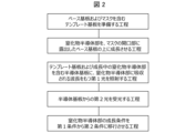
- FIG. 2 is a flow chart showing the method for manufacturing a semiconductor substrate according to this embodiment.
- FIG. 3 is a cross-sectional view showing the method for manufacturing a semiconductor substrate according to this embodiment.
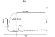
- FIG. 4 is a graph showing temporal changes in the reflectance, which is the ratio of the intensity of the second light to the intensity of the first light, and the set temperature.
- the method of manufacturing a semiconductor substrate according to the present embodiment includes a base substrate BS, a mask (mask pattern) 6 located on the base substrate BS and including a mask portion 5 and an opening KS. growing the nitride semiconductor portion 8 from the upper surface (base layer 4) of the base substrate BS exposed in the opening KS; a step of irradiating a semiconductor substrate 10 including a portion 8 with a first light L1 having a wavelength absorbed by the nitride semiconductor portion 8 at a growth temperature of the nitride semiconductor portion 8; A step of receiving light and a step of changing the growth condition of the nitride semiconductor portion 8 (shifting from the first condition to the second condition) are performed.
- the nitride semiconductor portion 8 and the mask portion 5 may be irradiated with the first light L1 in FIG. 3 and the like.
- the second light L2 includes the reflected light of the first light L1 from the upper surface of the nitride semiconductor portion 8 and the reflected light of the first light L1 from the upper surface of the mask portion 5. Using the second light L2, A transition from the first growth condition to the second growth condition may be initiated.
- the thickness direction of the mask portion 5 is defined as the vertical direction, and the width direction of the mask portion 5 is defined as the horizontal direction.
- the second condition may be a condition that prioritizes lateral growth (growth in the a-axis direction) of the nitride semiconductor portion 8 .
- the wavelength of the first light L1 may be included in the wavelength range of 395 to 415 nm.
- the relative level SL of the nitride semiconductor portion 8 with respect to the upper surface level UL of the mask portion 5 is detected in chronological order. A transition of growth conditions may be initiated.
- the growth condition may start to shift to the second condition, and after the shift, the growth may be performed under the second condition.
- the specified value in this case is 0.
- the transition may be started immediately after the relative level SL becomes zero.
- the prescribed value in this case is a positive value.
- the reflectance which is the ratio of the intensity of the second light L2 to the intensity of the first light L1
- the reflectance may vary periodically (appearance of fringes).
- the intensity of the first light L1 may be set to a fixed value, and the intensity of the second light L2 (reflected light intensity) may be acquired in time series. In this case, the intensity of the second light L2 (reflected light intensity ) fluctuates periodically.
- FIG. 5 is a graph showing temporal changes in the reflectance, which is the ratio of the intensity of the second light to the intensity of the first light, and the relative level.
- the number of cycles obtained along the time series may correspond to the relative level SL.
- the amount of increase in relative level SL per cycle may be a value according to the wavelength of first light L1 and the optical characteristics of mask portion 5 and nitride semiconductor portion 8 .
- the timing at which the predetermined number of cycles is detected may be the timing tc at which the relative level SL reaches the specified value (that is, the timing at which the transition of the growth conditions is started).
- the predetermined number in this case may be an integer, but is not limited to an integer.
- the timing of transition from initial growth (eg, vertical growth) to growth under different growth conditions (eg, lateral growth) is important.
- the transition timing is controlled by the deposition time, the transition timing may be too early or too late due to variations in the deposition rate due to factors such as the width of the opening and the characteristics of the manufacturing equipment, resulting in a decrease in manufacturing yield.
- the manufacturing yield is the rate at which nitride semiconductor parts that satisfy the compatibility conditions regarding, for example, dislocation density (defect density), aspect ratio, etc., are manufactured.
- light having a wavelength (for example, 405 nm) that is absorbed by the nitride semiconductor portion 8 at the growth temperature is used to reflect light from the surface of the nitride semiconductor portion 8 during growth and light reflected from the mask portion 5 .
- the growth state in the height direction (c-axis direction) can be monitored regardless of the internal structure of the base substrate BS by measuring the interference with BS as a fringe (shape of temporal change in physical quantity such as reflectance). .
- a wavelength e.g., 633 nm, 950 nm
- the nitride semiconductor part 8 for example, GaN crystal body
- the nitride semiconductor part 8 for example, GaN crystal body
- the nitride semiconductor is grown on the flat substrate without the mask pattern
- the inventors found that a fringe at 405 nm wavelength occurs which is not seen.
- the nitride semiconductor portion 8 high temperature of 1000° C. or higher
- light with a wavelength of 405 nm is absorbed by the nitride semiconductor (for example, GaN).
- a mask pattern including a silicon nitride film as the mask portion 5 interference of light reflected by the surface of the nitride semiconductor portion 8 and the surface of the mask portion 5 can be measured as a fringe.
- the ratio of the reflected light intensity to the incident light intensity on the upper surface of the nitride semiconductor portion 8 is higher than the ratio of the reflected light intensity to the incident light intensity on the upper surface of the mask portion 5 (reflectance of the mask portion). It can be big.
- the nitride semiconductor section 8 may have an absorption coefficient of the first light L1 at the growth temperature that is 10 times or more the absorption coefficient of the first light L1 at room temperature.
- the bandgap of nitride semiconductor portion 8 at the growth temperature may be smaller than the bandgap of nitride semiconductor portion 8 at room temperature (3.4 eV in the case of GaN).
- the wavelength of the first light L1 may be set according to the bandgap of the nitride semiconductor portion 8 at the growth temperature.
- the first light L1 may be laser light.
- the nitride semiconductor portion 8 includes a GaN-based semiconductor, the growth conditions include the growth temperature, and the growth temperature is preferably a temperature suitable for vertical growth in the first temperature, which is the first condition, and is the second condition. It may be lower than the second temperature.
- the growth conditions may include the flow rate of the raw material gas containing gallium, and the flow rate of the raw material gas may be lower than the second flow rate, which is the second condition.
- the width of the mask portion 5 may be 20 [ ⁇ m] or more.
- the ratio of the thickness of mask portion 5 to the width of opening KS may be 3.0 or less.
- FIG. 6 is a plan view showing an example of a mask.
- the opening KS of the mask 6 (mask pattern) exposes the upper surface of the base substrate and has the function of a growth start opening for starting the growth of the nitride semiconductor portion 8 . It may have the function of a selective growth mask for directional growth.
- the opening KS is a portion (non-formation portion) of the mask pattern 6 where the mask portion 5 is absent, and may not be surrounded by the mask portion 5 .
- an inorganic film ZF inorganic insulating film
- a silicon oxide (SiOx) film, a silicon nitride (SiNx) film, a silicon oxynitride film (SiON), or a titanium nitride (TiNx) film can be used.
- the opening KS has a longitudinal shape, and a plurality of openings KS may be periodically arranged in the ⁇ 11-20> direction (a-axis direction) of the nitride semiconductor portion 8 .
- the width of the opening KS may be about 0.2 ⁇ m to 20 ⁇ m.
- the nitride semiconductor portion 8 can be easily peeled off in a post-process (described later).
- the mask 6 can also be a layered film containing the above materials (for example, at least two of silicon oxide, silicon nitride, and silicon oxynitride).
- a plurality of longitudinal inorganic films ZF each functioning as a mask portion 5 are separated from the nitride semiconductor portion 8 by a plurality of gaps ZN functioning as openings KS. > direction (a-axis direction).
- a plurality of longitudinal inorganic films ZF may be aligned in the ⁇ 11-20> direction (a-axis direction) and in the ⁇ 1-100> direction (m-axis direction).
- FIG. 7 is a cross-sectional view showing a configuration example of the base substrate.
- the base substrate BS may have the main substrate 1 which is a different substrate having a lattice constant different from that of the nitride semiconductor portion 8 .
- the nitride semiconductor portion 8 may contain a GaN-based semiconductor, and the main substrate 1, which is a heterosubstrate, may be a silicon substrate.
- heterogeneous substrates include silicon substrates, sapphire (Al 2 O 3 ) substrates, silicon carbide (SiC) substrates, and the like.
- the plane orientation of the main substrate 1 is, for example, the (111) plane of the silicon substrate, the (0001) plane of the sapphire substrate, and the 6H-SiC (0001) and 4H-SiC (0001) planes of the SiC substrate. These are only examples, and any substrate and plane orientation may be used as long as the nitride semiconductor portion 8 can be grown by the ELO method.
- the base substrate BS may include the main substrate 1 and the underlying portion 4 on the main substrate 1, and the nitride semiconductor portion 8 may grow from the upper surface of the underlying portion 4 exposed in the opening KS.
- the underlying portion 4 may contain a GaN-based semiconductor.
- the underlying portion 4 may include at least one of a seed portion and a buffer portion.
- a GaN-based semiconductor can be used as the seed portion.
- a GaN-based semiconductor, AlN, SiC, or the like can be used as the buffer portion.
- the base substrate BS may be composed of a self-supporting single crystal substrate such as GaN or SiC (for example, a wafer cut from a bulk crystal), and the mask 6 may be arranged on the single crystal substrate.
- FIG. 8 is a schematic diagram showing the configuration of the semiconductor substrate manufacturing apparatus according to this embodiment.
- a semiconductor substrate manufacturing apparatus 20 includes a base substrate BS, and a stage 21 on which a template substrate TS having a mask pattern including a mask portion and an opening is placed on the base substrate BS.
- a raw material supply device 22 for supplying a raw material for growing the nitride semiconductor portion 8 on the template substrate TS;
- An optical device 23 that emits a first light L1 having a wavelength that is absorbed by the nitride semiconductor portion 8 at the growth temperature and receives a second light L2 from the semiconductor substrate 10, and growth conditions for the nitride semiconductor portion 8.
- the control device 24 may be capable of at least one of wired communication and wireless communication with the optical device 23 .
- a semiconductor substrate manufacturing apparatus 20 is provided with a chamber 25 including a stage SG, a flow channel 27 passing through the chamber 25, and a heating device 26 for heating the chamber 25, and the semiconductor substrate 10 is arranged in the flow channel 27. good.
- the control device 22 may use the intensity of the second light L2 to instruct the heating device 26 to shift from the first condition (first temperature) to the second condition (second temperature>first temperature).
- Optical device 23 may be located outside chamber 25 .
- the chamber 25 may be provided with a window 28 through which the first light L1 and the second light L2 are transmitted.
- the stage 21 may rotate (with the axis in the normal direction of the template substrate TS as the rotation axis).
- the raw material supply device 22 causes the raw material gas to flow sideways (in a direction parallel to the upper surface of the template substrate) in the flow channel 27 under the first and second conditions, and the gas is discharged sideways. not.
- the raw material gas can also flow vertically (in the direction normal to the template substrate TS) under the first and second conditions.
- the control device 24 uses the intensity of the second light L2 to detect the relative level of the upper surface of the nitride semiconductor portion 8 with the upper surface level UL of the mask portion 5 as a reference in chronological order, and the relative level reaches the specified value. Even if the raw material supply device 22 is instructed to shift from the first condition (for example, the first flow rate) to the second condition (for example, the second flow rate > the first flow rate) at the timing (see tc in FIG. 5) At this timing, the heating device 26 may be instructed to shift from the first condition (first temperature) to the second condition (second temperature>first temperature).
- the control device 24 may be configured to control at least one of the raw material supply device 22 and the heating device 26 by executing a program stored in an internal memory, a communicable communication device, or an accessible network, for example. , this program, and a recording medium storing this program are also included in this embodiment.
- FIG. 9 is a cross-sectional view showing the method for manufacturing the semiconductor substrate according to the first embodiment.
- a base portion 4 containing a nitride semiconductor is formed on a main substrate 1 , and a mask pattern 6 including a plurality of striped mask portions 5 is provided on the base portion 4 .
- the mask 5 portion is made of a silicon nitride film having a film thickness of 100 nm and a width of 52 ⁇ m, and the m-axis direction of the nitride semiconductor portion 8 is taken as a longitudinal direction.
- the pitch of the stripes of the mask portion 5 is set to 55 ⁇ m.
- a resist stripe pattern is formed by photolithography on the base substrate BS on which the nitride semiconductor film is formed as the underlying portion 4 .
- a silicon nitride film having a thickness of 100 nm is formed over the entire surface by a sputtering method.
- the silicon nitride film is patterned by a lift-off method to form a mask pattern 6 (stripe pattern).
- the nitride semiconductor portion 8 including the initial growth portion 8s is grown on the mask pattern 6 by metal organic chemical vapor deposition (MOCVD) using trimethylgallium (TMG) and ammonia (NH 3 ) (ELO method).
- MOCVD metal organic chemical vapor deposition
- TMG trimethylgallium
- NH 3 ammonia
- an initial growth portion 8s is formed above the underlying portion 4 exposed in the opening KS.
- the growth condition be the first condition.
- the transition of the growth condition (from the first condition to the second condition) is started.
- the semiconductor element device
- Example 1 the film thickness monitoring technique described in the embodiment was used, and the first condition (condition for giving priority to longitudinal growth) was set as follows. Growth temperature (set temperature): 1100° C. (first temperature), growth pressure: 10 kPa, ammonia flow rate: 7.5 slm, trimethylgallium flow rate: 3 sccm. Also, the second condition (condition for giving priority to lateral growth) is set as follows. Growth temperature (set temperature): 1175° C. (second temperature), growth pressure: 10 kPa, ammonia flow rate: 7.5 slm, trimethylgallium flow rate: 11 sccm.
- the initial growth portion 8s serves as a starting point for lateral growth of the nitride semiconductor portion 8 .
- the initial growth layer 8s can be formed with a thickness of, for example, 30 nm to 1000 nm, 50 nm to 400 nm, or 70 nm to 350 nm.
- the width of the gap GP can be 5 ⁇ m or less, 3 ⁇ m or less, or 2 ⁇ m or less.
- the portion located on the initial growth portion 8s becomes a dislocation propagating portion with many threading dislocations, and the portion (wing portion) on the mask portion 5 has more threading dislocations than the dislocation propagating portion.
- a low defect portion YS having a density of 1/10 or less is obtained.
- a threading dislocation is a dislocation (defect) extending in the c-axis direction ( ⁇ 0001> direction) of the nitride semiconductor portion 8 .
- the threading dislocation density of the low defect portion YS can be, for example, 5 ⁇ 10 6 [pieces/cm 2 ] or less.
- the ratio of the size W1 in the a-axis direction to the thickness d1 can be, for example, 2.0 or more.
- W1/d1 can be set to 1.5 or more, 2.0 or more, 4.0 or more, 5.0 or more, 7.0 or more, or 10.0 or more. It is known that setting W1/d1 to 1.5 or more facilitates the step of dividing the nitride semiconductor portion 8 (for example, the step of dividing the nitride semiconductor portion 8 into an m-plane cross section) in a subsequent process. Moreover, the internal stress of the nitride semiconductor portion 8 is reduced, and the warp of the semiconductor substrate 10 is reduced.
- the nitride semiconductor portion 8 (including the initial growth portion 8s) shown in FIG. 9 can be a nitride semiconductor crystal (eg, GaN crystal, AlGaN crystal, InGaN crystal, or InAlGaN crystal).
- FIG. 10 is a cross-sectional view showing a method for manufacturing a semiconductor device according to a second embodiment; 10 includes a step of forming the compound semiconductor portion 9 and the electrodes D1 and D2 on the semiconductor substrate 10 after preparing the semiconductor substrate 10 described above, and a step of forming the nitride semiconductor portion 8, the compound semiconductor portion 9 and the electrodes D1 and D2.
- the mask 6 may be removed by wet etching or the like before removing the base substrate BS.
- the nitride semiconductor portion 8 may be an n-type semiconductor crystal.
- the compound semiconductor portion 9 may contain a GaN-based semiconductor.
- the compound semiconductor portion 9 may include an active portion (for example, an active layer such as a quantum well structure) and a p-type semiconductor portion, or may include an n-type semiconductor portion (for example, a regrowth layer, an n-type contact layer) under the active portion. good.
- the active portion of the compound semiconductor portion 9 includes a light-emitting portion
- the light-emitting portion can be arranged above the low-defect portion YS (overlapping the low-defect portion YS in plan view). Thereby, luminous efficiency can be improved.
- the electrode D1 positioned above the low-defect portion YS may be the anode, and the electrode D2 may be the cathode.
- the support substrate SK may have a conductive pad in contact with the bonding layer H1 and a conductive pad in contact with the bonding layer H2.
- the joining layers H1 and H2 may be made of a solder material.
- the longitudinal laminate EB may be divided into a plurality of pieces (by cutting in the lateral direction). The division step may be performed by cleaving the portion 9 (for example, m-plane cleavage in which the cleavage plane is the m-plane).
- the m-plane which is a cleavage plane, may be coated (formed with a reflector film) on the facet.
- the laminate EB is transferred from the base substrate BS to the support substrate SK in FIG. 10, the present invention is not limited to this. It may be transferred from the base substrate BS to a tape or the like one or more times.
- the semiconductor element SD may function as an LED (light emitting diode) element or a semiconductor laser element.
- the support ST may be a submount substrate.
- Example 2 includes an electronic device (for example, a lighting device, a laser device, a display device, a measuring device, an information processing device, etc.) having a semiconductor element SD.
- FIG. 11 is a cross-sectional view showing the method for manufacturing the semiconductor substrate of this embodiment.
- the method of manufacturing a semiconductor substrate according to the present embodiment includes steps of preparing a template substrate TS having a seed region SA and a growth suppression region YA on the upper surface side, and growing the nitride semiconductor portion 8 from the upper surface of the seed region SA.
- the first light L1 in FIG. 11 may irradiate the nitride semiconductor portion 8 and the growth suppression region YA.
- the second light L2 includes the reflected light of the first light L1 from the upper surface of the nitride semiconductor portion 8 and the reflected light of the first light L1 from the growth suppression region YA. A transition from the first growth condition to the second growth condition may be initiated.
- the first condition is a condition that prioritizes the growth of the nitride semiconductor portion 8 in the vertical direction (growth in the c-axis direction)
- the second condition may be a condition that prioritizes lateral growth (growth in the a-axis direction) of the nitride semiconductor portion 8 .
- the wavelength of the first light L1 may be included in the wavelength range of 395 to 415 nm.
- the relative level SL of the nitride semiconductor portion 8 with respect to the level YL of the growth suppression region YA is detected in chronological order. A transition of growth conditions may be initiated.
- the growth condition is the first condition
- the relative level SL is less than the specified value
- the relative level SL reaches the specified value (for example, 10 nm to 500 nm).
- the seed region SA only needs to be made of a material from which the nitride semiconductor portion 8 grows. ) crystalline materials with a small lattice constant gap.
- the growth suppression region YA may be made of a material that suppresses the vertical growth (for example, the growth in the c-axis direction) of the nitride semiconductor portion 8.
- an amorphous material such as silicon nitride or silicon oxide, or a semiconductor such as SiC may be used.
- polycrystalline materials or metallic materials may be mentioned.
Landscapes
- Chemical & Material Sciences (AREA)
- Metallurgy (AREA)
- Engineering & Computer Science (AREA)
- Crystallography & Structural Chemistry (AREA)
- Materials Engineering (AREA)
- Organic Chemistry (AREA)
- General Chemical & Material Sciences (AREA)
- Chemical Kinetics & Catalysis (AREA)
- Inorganic Chemistry (AREA)
- Physics & Mathematics (AREA)
- Electromagnetism (AREA)
- Optics & Photonics (AREA)
- Crystals, And After-Treatments Of Crystals (AREA)
- Recrystallisation Techniques (AREA)
- Chemical Vapour Deposition (AREA)
Priority Applications (4)
| Application Number | Priority Date | Filing Date | Title |
|---|---|---|---|
| EP23747009.1A EP4471833A4 (en) | 2022-01-27 | 2023-01-26 | METHOD FOR MANUFACTURING AND DEVICE FOR MANUFACTURING SEMICONDUCTIVE SUBSTRATE AND CONTROL DEVICE |
| KR1020247024650A KR20240119154A (ko) | 2022-01-27 | 2023-01-26 | 반도체 기판의 제조 방법 및 제조 장치, 및 제어 장치 |
| JP2023576962A JP7745660B2 (ja) | 2022-01-27 | 2023-01-26 | 半導体基板の製造方法、半導体基板の製造装置 |
| US18/832,370 US20250118554A1 (en) | 2022-01-27 | 2023-01-26 | Manufacturing method and manufacturing apparatus of semiconductor substrate, and control device |
Applications Claiming Priority (2)
| Application Number | Priority Date | Filing Date | Title |
|---|---|---|---|
| JP2022-011293 | 2022-01-27 | ||
| JP2022011293 | 2022-01-27 |
Publications (1)
| Publication Number | Publication Date |
|---|---|
| WO2023145799A1 true WO2023145799A1 (ja) | 2023-08-03 |
Family
ID=87471545
Family Applications (1)
| Application Number | Title | Priority Date | Filing Date |
|---|---|---|---|
| PCT/JP2023/002374 Ceased WO2023145799A1 (ja) | 2022-01-27 | 2023-01-26 | 半導体基板の製造方法および製造装置、並びに制御装置 |
Country Status (6)
| Country | Link |
|---|---|
| US (1) | US20250118554A1 (https=) |
| EP (1) | EP4471833A4 (https=) |
| JP (1) | JP7745660B2 (https=) |
| KR (1) | KR20240119154A (https=) |
| TW (1) | TWI864562B (https=) |
| WO (1) | WO2023145799A1 (https=) |
Citations (9)
| Publication number | Priority date | Publication date | Assignee | Title |
|---|---|---|---|---|
| JP2004273661A (ja) * | 2003-03-07 | 2004-09-30 | Sumitomo Chem Co Ltd | 窒化ガリウム単結晶基板の製造方法 |
| JP2006114829A (ja) * | 2004-10-18 | 2006-04-27 | Rohm Co Ltd | 半導体装置およびその製造方法、ならびに半導体装置のための基板 |
| JP2007099567A (ja) * | 2005-10-05 | 2007-04-19 | Furukawa Co Ltd | Iii族窒化物半導体層の形成方法、iii族窒化物半導体基板の製造方法およびiii族窒化物半導体基板 |
| JP2012503340A (ja) * | 2008-09-19 | 2012-02-02 | 台湾積體電路製造股▲ふん▼有限公司 | エピタキシャル層の成長によるデバイス形成 |
| JP2012517114A (ja) * | 2009-02-05 | 2012-07-26 | ソイテック | 半導体材料を形成するためのエピタキシャル方法および構造 |
| JP2013147383A (ja) * | 2012-01-19 | 2013-08-01 | Sharp Corp | 窒化物半導体ウエハおよび窒化物半導体ウエハの製造方法 |
| JP2013251304A (ja) | 2012-05-30 | 2013-12-12 | Furukawa Co Ltd | 積層体および積層体の製造方法 |
| JP2015109389A (ja) * | 2013-12-05 | 2015-06-11 | 日本電信電話株式会社 | 化合物半導体の成長方法 |
| WO2021085556A1 (ja) * | 2019-10-29 | 2021-05-06 | 京セラ株式会社 | 半導体素子および半導体素子の製造方法 |
Family Cites Families (2)
| Publication number | Priority date | Publication date | Assignee | Title |
|---|---|---|---|---|
| TW200703463A (en) * | 2005-05-31 | 2007-01-16 | Univ California | Defect reduction of non-polar and semi-polar III-nitrides with sidewall lateral epitaxial overgrowth (SLEO) |
| EP2743966B1 (en) * | 2012-12-14 | 2020-11-25 | Seoul Viosys Co., Ltd. | Epitaxial layer wafer having void for separating growth substrate therefrom and semiconductor device fabricated using the same |
-
2023
- 2023-01-19 TW TW112102540A patent/TWI864562B/zh active
- 2023-01-26 WO PCT/JP2023/002374 patent/WO2023145799A1/ja not_active Ceased
- 2023-01-26 JP JP2023576962A patent/JP7745660B2/ja active Active
- 2023-01-26 EP EP23747009.1A patent/EP4471833A4/en active Pending
- 2023-01-26 US US18/832,370 patent/US20250118554A1/en active Pending
- 2023-01-26 KR KR1020247024650A patent/KR20240119154A/ko active Pending
Patent Citations (9)
| Publication number | Priority date | Publication date | Assignee | Title |
|---|---|---|---|---|
| JP2004273661A (ja) * | 2003-03-07 | 2004-09-30 | Sumitomo Chem Co Ltd | 窒化ガリウム単結晶基板の製造方法 |
| JP2006114829A (ja) * | 2004-10-18 | 2006-04-27 | Rohm Co Ltd | 半導体装置およびその製造方法、ならびに半導体装置のための基板 |
| JP2007099567A (ja) * | 2005-10-05 | 2007-04-19 | Furukawa Co Ltd | Iii族窒化物半導体層の形成方法、iii族窒化物半導体基板の製造方法およびiii族窒化物半導体基板 |
| JP2012503340A (ja) * | 2008-09-19 | 2012-02-02 | 台湾積體電路製造股▲ふん▼有限公司 | エピタキシャル層の成長によるデバイス形成 |
| JP2012517114A (ja) * | 2009-02-05 | 2012-07-26 | ソイテック | 半導体材料を形成するためのエピタキシャル方法および構造 |
| JP2013147383A (ja) * | 2012-01-19 | 2013-08-01 | Sharp Corp | 窒化物半導体ウエハおよび窒化物半導体ウエハの製造方法 |
| JP2013251304A (ja) | 2012-05-30 | 2013-12-12 | Furukawa Co Ltd | 積層体および積層体の製造方法 |
| JP2015109389A (ja) * | 2013-12-05 | 2015-06-11 | 日本電信電話株式会社 | 化合物半導体の成長方法 |
| WO2021085556A1 (ja) * | 2019-10-29 | 2021-05-06 | 京セラ株式会社 | 半導体素子および半導体素子の製造方法 |
Non-Patent Citations (1)
| Title |
|---|
| See also references of EP4471833A4 |
Also Published As
| Publication number | Publication date |
|---|---|
| TW202341251A (zh) | 2023-10-16 |
| EP4471833A1 (en) | 2024-12-04 |
| EP4471833A4 (en) | 2025-12-31 |
| US20250118554A1 (en) | 2025-04-10 |
| JP7745660B2 (ja) | 2025-09-29 |
| JPWO2023145799A1 (https=) | 2023-08-03 |
| KR20240119154A (ko) | 2024-08-06 |
| TWI864562B (zh) | 2024-12-01 |
Similar Documents
| Publication | Publication Date | Title |
|---|---|---|
| US7030417B2 (en) | Semiconductor light emitting device and fabrication method thereof | |
| JP2003218390A (ja) | 半導体発光素子及びその製造方法 | |
| JP2002313742A (ja) | 窒化物半導体の気相成長方法及び窒化物半導体素子 | |
| EP1378934A1 (en) | Production method of iii nitride compound semiconductor, and iii nitride compound semiconductor element based on it | |
| US9899564B2 (en) | Group III nitride semiconductor and method for producing same | |
| JP5073624B2 (ja) | 酸化亜鉛系半導体の成長方法及び半導体発光素子の製造方法 | |
| US8148178B2 (en) | Method of growing nitride single crystal and method of manufacturing nitride semiconductor light emitting device | |
| JP2003031844A (ja) | 半導体発光素子の製造方法 | |
| TWI892104B (zh) | 半導體基板 | |
| KR101505119B1 (ko) | 3족 질화물 반도체층을 제조하는 방법 | |
| JP7745660B2 (ja) | 半導体基板の製造方法、半導体基板の製造装置 | |
| TWI899553B (zh) | 半導體基板之製造方法及製造裝置 | |
| KR101505121B1 (ko) | 3족 질화물 반도체층을 제조하는 방법 | |
| JP4232326B2 (ja) | 低欠陥窒化物半導体の成長方法 | |
| JP5073623B2 (ja) | 酸化亜鉛系半導体の成長方法及び半導体発光素子の製造方法 | |
| JP3555657B2 (ja) | 低欠陥窒化物半導体基板及びその製造方法 | |
| JP7637237B2 (ja) | 半導体デバイスの製造方法および製造装置 | |
| JP2003218468A (ja) | 半導体レーザ素子及びその製造方法 | |
| JP2005020027A (ja) | 窒化ガリウム系化合物半導体の製造方法 | |
| WO2025018196A1 (ja) | 半導体基板の製造方法、半導体基板の製造装置およびテンプレート基板 | |
| JP2003115605A (ja) | 半導体発光素子及びその製造方法 |
Legal Events
| Date | Code | Title | Description |
|---|---|---|---|
| 121 | Ep: the epo has been informed by wipo that ep was designated in this application |
Ref document number: 23747009 Country of ref document: EP Kind code of ref document: A1 |
|
| ENP | Entry into the national phase |
Ref document number: 20247024650 Country of ref document: KR Kind code of ref document: A |
|
| WWE | Wipo information: entry into national phase |
Ref document number: 18832370 Country of ref document: US |
|
| ENP | Entry into the national phase |
Ref document number: 2023576962 Country of ref document: JP Kind code of ref document: A |
|
| NENP | Non-entry into the national phase |
Ref country code: DE |
|
| ENP | Entry into the national phase |
Ref document number: 2023747009 Country of ref document: EP Effective date: 20240827 |
|
| WWP | Wipo information: published in national office |
Ref document number: 18832370 Country of ref document: US |