WO2023145799A1 - Semiconductor substrate manufacturing method and manufacturing device, and control device - Google Patents
Semiconductor substrate manufacturing method and manufacturing device, and control device Download PDFInfo
- Publication number
- WO2023145799A1 WO2023145799A1 PCT/JP2023/002374 JP2023002374W WO2023145799A1 WO 2023145799 A1 WO2023145799 A1 WO 2023145799A1 JP 2023002374 W JP2023002374 W JP 2023002374W WO 2023145799 A1 WO2023145799 A1 WO 2023145799A1
- Authority
- WO
- WIPO (PCT)
- Prior art keywords
- nitride semiconductor
- light
- manufacturing
- condition
- mask
- Prior art date
Links
Images


Classifications
-
- C—CHEMISTRY; METALLURGY
- C30—CRYSTAL GROWTH
- C30B—SINGLE-CRYSTAL GROWTH; UNIDIRECTIONAL SOLIDIFICATION OF EUTECTIC MATERIAL OR UNIDIRECTIONAL DEMIXING OF EUTECTOID MATERIAL; REFINING BY ZONE-MELTING OF MATERIAL; PRODUCTION OF A HOMOGENEOUS POLYCRYSTALLINE MATERIAL WITH DEFINED STRUCTURE; SINGLE CRYSTALS OR HOMOGENEOUS POLYCRYSTALLINE MATERIAL WITH DEFINED STRUCTURE; AFTER-TREATMENT OF SINGLE CRYSTALS OR A HOMOGENEOUS POLYCRYSTALLINE MATERIAL WITH DEFINED STRUCTURE; APPARATUS THEREFOR
- C30B25/00—Single-crystal growth by chemical reaction of reactive gases, e.g. chemical vapour-deposition growth
- C30B25/02—Epitaxial-layer growth
- C30B25/04—Pattern deposit, e.g. by using masks
-
- C—CHEMISTRY; METALLURGY
- C30—CRYSTAL GROWTH
- C30B—SINGLE-CRYSTAL GROWTH; UNIDIRECTIONAL SOLIDIFICATION OF EUTECTIC MATERIAL OR UNIDIRECTIONAL DEMIXING OF EUTECTOID MATERIAL; REFINING BY ZONE-MELTING OF MATERIAL; PRODUCTION OF A HOMOGENEOUS POLYCRYSTALLINE MATERIAL WITH DEFINED STRUCTURE; SINGLE CRYSTALS OR HOMOGENEOUS POLYCRYSTALLINE MATERIAL WITH DEFINED STRUCTURE; AFTER-TREATMENT OF SINGLE CRYSTALS OR A HOMOGENEOUS POLYCRYSTALLINE MATERIAL WITH DEFINED STRUCTURE; APPARATUS THEREFOR
- C30B29/00—Single crystals or homogeneous polycrystalline material with defined structure characterised by the material or by their shape
- C30B29/10—Inorganic compounds or compositions
- C30B29/38—Nitrides
-
- H—ELECTRICITY
- H01—ELECTRIC ELEMENTS
- H01L—SEMICONDUCTOR DEVICES NOT COVERED BY CLASS H10
- H01L21/00—Processes or apparatus adapted for the manufacture or treatment of semiconductor or solid state devices or of parts thereof
- H01L21/02—Manufacture or treatment of semiconductor devices or of parts thereof
- H01L21/04—Manufacture or treatment of semiconductor devices or of parts thereof the devices having at least one potential-jump barrier or surface barrier, e.g. PN junction, depletion layer or carrier concentration layer
- H01L21/18—Manufacture or treatment of semiconductor devices or of parts thereof the devices having at least one potential-jump barrier or surface barrier, e.g. PN junction, depletion layer or carrier concentration layer the devices having semiconductor bodies comprising elements of Group IV of the Periodic System or AIIIBV compounds with or without impurities, e.g. doping materials
- H01L21/20—Deposition of semiconductor materials on a substrate, e.g. epitaxial growth solid phase epitaxy
- H01L21/2003—Deposition of semiconductor materials on a substrate, e.g. epitaxial growth solid phase epitaxy characterised by the substrate
- H01L21/2015—Deposition of semiconductor materials on a substrate, e.g. epitaxial growth solid phase epitaxy characterised by the substrate the substrate being of crystalline semiconductor material, e.g. lattice adaptation, heteroepitaxy
Definitions
- the present disclosure relates to a semiconductor substrate manufacturing method, a manufacturing apparatus, and a control apparatus.
- Patent Document 1 discloses a method of forming a GaN-based semiconductor layer on a GaN-based substrate or a heterogeneous substrate (for example, a sapphire substrate) using an ELO (Epitaxial Lateral Overgrowth) method.
- ELO Epiaxial Lateral Overgrowth
- a method for manufacturing a semiconductor substrate according to the present disclosure includes steps of preparing a template substrate having a base substrate and a mask positioned on the base substrate and including a mask portion and an opening; growing from a base substrate exposed to the second substrate, and growing the semiconductor substrate including the template substrate and the nitride semiconductor portion being grown on the semiconductor substrate having a wavelength that is absorbed by the nitride semiconductor portion at the growth temperature of the nitride semiconductor portion.
- the method includes a step of irradiating one light, a step of receiving a second light from the semiconductor substrate, and a step of changing growth conditions of the nitride semiconductor portion.
- FIG. 1 is a schematic diagram showing the configuration of a semiconductor substrate manufacturing apparatus according to an embodiment;
- FIG. 1 is a schematic diagram showing the configuration of a semiconductor substrate manufacturing apparatus according to an embodiment;
- FIG. FIG. 1 is a schematic diagram showing the configuration of a semiconductor substrate manufacturing apparatus according to an embodiment;
- FIG. FIG. 1 is a schematic diagram showing the configuration of a semiconductor substrate manufacturing apparatus according to an embodiment;
- FIG. FIG. 1 is a schematic diagram showing the configuration of a semiconductor substrate manufacturing apparatus according to an embodiment;
- FIG. 3 is a cross-sectional view showing a method for manufacturing a semiconductor substrate according to Example 1;
- FIG. 10 is a cross-sectional view showing a method for manufacturing a semiconductor device according to Example 2; It is sectional drawing which shows the manufacturing method of the semiconductor substrate of this embodiment.
- FIG. 1 is a cross-sectional view showing the configuration of a semiconductor substrate according to this embodiment.
- the semiconductor substrate 10 semiconductor wafer
- the semiconductor substrate 10 semiconductor wafer
- the semiconductor substrate 10 includes a base substrate BS, a mask (mask pattern) 6 formed on the base substrate and having an opening KS and a mask portion 5, and a nitride semiconductor portion 8 arranged from above the base substrate BS exposed in the opening KS to above the mask portion 5 .
- the mask 5 may be a mask layer
- the nitride semiconductor portion 8 may be a nitride semiconductor layer.
- the nitride semiconductor portion 8 contains a nitride semiconductor as a main material.
- a GaN-based semiconductor is a semiconductor containing gallium atoms (Ga) and nitrogen atoms (N), and typical examples include GaN, AlGaN, AlGaInN, and InGaN.
- the nitride semiconductor portion 8 may be of a doped type (for example, n-type containing donors) or non-doped type.
- a semiconductor substrate means a substrate containing a nitride semiconductor, and the base substrate BS may contain a semiconductor other than a nitride semiconductor (eg, silicon-based semiconductor, SiC, gallium oxide) or a non-semiconductor (sapphire). .
- the base substrate BS and the mask 6 are sometimes called a template substrate TS.
- the nitride semiconductor portion 8 can be formed by an ELO (Epitaxial Lateral Overgrowth) method, starting from the base substrate BS exposed from the opening KS.
- the thickness direction of the nitride semiconductor portion 8 may be the c-axis direction ( ⁇ 0001> direction).
- the opening KS has a longitudinal shape, and its width direction may be the a-axis direction ( ⁇ 11-20> direction) of the nitride semiconductor portion 8 .
- the direction from the base substrate BS to the nitride semiconductor portion 8 is "upward". Viewing an object with a line of sight parallel to the normal direction of the semiconductor substrate 10 (including perspective) is sometimes referred to as “plan view”.
- FIG. 2 is a flow chart showing the method for manufacturing a semiconductor substrate according to this embodiment.
- FIG. 3 is a cross-sectional view showing the method for manufacturing a semiconductor substrate according to this embodiment.
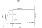
- FIG. 4 is a graph showing temporal changes in the reflectance, which is the ratio of the intensity of the second light to the intensity of the first light, and the set temperature.
- the method of manufacturing a semiconductor substrate according to the present embodiment includes a base substrate BS, a mask (mask pattern) 6 located on the base substrate BS and including a mask portion 5 and an opening KS. growing the nitride semiconductor portion 8 from the upper surface (base layer 4) of the base substrate BS exposed in the opening KS; a step of irradiating a semiconductor substrate 10 including a portion 8 with a first light L1 having a wavelength absorbed by the nitride semiconductor portion 8 at a growth temperature of the nitride semiconductor portion 8; A step of receiving light and a step of changing the growth condition of the nitride semiconductor portion 8 (shifting from the first condition to the second condition) are performed.
- the nitride semiconductor portion 8 and the mask portion 5 may be irradiated with the first light L1 in FIG. 3 and the like.
- the second light L2 includes the reflected light of the first light L1 from the upper surface of the nitride semiconductor portion 8 and the reflected light of the first light L1 from the upper surface of the mask portion 5. Using the second light L2, A transition from the first growth condition to the second growth condition may be initiated.
- the thickness direction of the mask portion 5 is defined as the vertical direction, and the width direction of the mask portion 5 is defined as the horizontal direction.
- the second condition may be a condition that prioritizes lateral growth (growth in the a-axis direction) of the nitride semiconductor portion 8 .
- the wavelength of the first light L1 may be included in the wavelength range of 395 to 415 nm.
- the relative level SL of the nitride semiconductor portion 8 with respect to the upper surface level UL of the mask portion 5 is detected in chronological order. A transition of growth conditions may be initiated.
- the growth condition may start to shift to the second condition, and after the shift, the growth may be performed under the second condition.
- the specified value in this case is 0.
- the transition may be started immediately after the relative level SL becomes zero.
- the prescribed value in this case is a positive value.
- the reflectance which is the ratio of the intensity of the second light L2 to the intensity of the first light L1
- the reflectance may vary periodically (appearance of fringes).
- the intensity of the first light L1 may be set to a fixed value, and the intensity of the second light L2 (reflected light intensity) may be acquired in time series. In this case, the intensity of the second light L2 (reflected light intensity ) fluctuates periodically.
- FIG. 5 is a graph showing temporal changes in the reflectance, which is the ratio of the intensity of the second light to the intensity of the first light, and the relative level.
- the number of cycles obtained along the time series may correspond to the relative level SL.
- the amount of increase in relative level SL per cycle may be a value according to the wavelength of first light L1 and the optical characteristics of mask portion 5 and nitride semiconductor portion 8 .
- the timing at which the predetermined number of cycles is detected may be the timing tc at which the relative level SL reaches the specified value (that is, the timing at which the transition of the growth conditions is started).
- the predetermined number in this case may be an integer, but is not limited to an integer.
- the timing of transition from initial growth (eg, vertical growth) to growth under different growth conditions (eg, lateral growth) is important.
- the transition timing is controlled by the deposition time, the transition timing may be too early or too late due to variations in the deposition rate due to factors such as the width of the opening and the characteristics of the manufacturing equipment, resulting in a decrease in manufacturing yield.
- the manufacturing yield is the rate at which nitride semiconductor parts that satisfy the compatibility conditions regarding, for example, dislocation density (defect density), aspect ratio, etc., are manufactured.
- light having a wavelength (for example, 405 nm) that is absorbed by the nitride semiconductor portion 8 at the growth temperature is used to reflect light from the surface of the nitride semiconductor portion 8 during growth and light reflected from the mask portion 5 .
- the growth state in the height direction (c-axis direction) can be monitored regardless of the internal structure of the base substrate BS by measuring the interference with BS as a fringe (shape of temporal change in physical quantity such as reflectance). .
- a wavelength e.g., 633 nm, 950 nm
- the nitride semiconductor part 8 for example, GaN crystal body
- the nitride semiconductor part 8 for example, GaN crystal body
- the nitride semiconductor is grown on the flat substrate without the mask pattern
- the inventors found that a fringe at 405 nm wavelength occurs which is not seen.
- the nitride semiconductor portion 8 high temperature of 1000° C. or higher
- light with a wavelength of 405 nm is absorbed by the nitride semiconductor (for example, GaN).
- a mask pattern including a silicon nitride film as the mask portion 5 interference of light reflected by the surface of the nitride semiconductor portion 8 and the surface of the mask portion 5 can be measured as a fringe.
- the ratio of the reflected light intensity to the incident light intensity on the upper surface of the nitride semiconductor portion 8 is higher than the ratio of the reflected light intensity to the incident light intensity on the upper surface of the mask portion 5 (reflectance of the mask portion). It can be big.
- the nitride semiconductor section 8 may have an absorption coefficient of the first light L1 at the growth temperature that is 10 times or more the absorption coefficient of the first light L1 at room temperature.
- the bandgap of nitride semiconductor portion 8 at the growth temperature may be smaller than the bandgap of nitride semiconductor portion 8 at room temperature (3.4 eV in the case of GaN).
- the wavelength of the first light L1 may be set according to the bandgap of the nitride semiconductor portion 8 at the growth temperature.
- the first light L1 may be laser light.
- the nitride semiconductor portion 8 includes a GaN-based semiconductor, the growth conditions include the growth temperature, and the growth temperature is preferably a temperature suitable for vertical growth in the first temperature, which is the first condition, and is the second condition. It may be lower than the second temperature.
- the growth conditions may include the flow rate of the raw material gas containing gallium, and the flow rate of the raw material gas may be lower than the second flow rate, which is the second condition.
- the width of the mask portion 5 may be 20 [ ⁇ m] or more.
- the ratio of the thickness of mask portion 5 to the width of opening KS may be 3.0 or less.
- FIG. 6 is a plan view showing an example of a mask.
- the opening KS of the mask 6 (mask pattern) exposes the upper surface of the base substrate and has the function of a growth start opening for starting the growth of the nitride semiconductor portion 8 . It may have the function of a selective growth mask for directional growth.
- the opening KS is a portion (non-formation portion) of the mask pattern 6 where the mask portion 5 is absent, and may not be surrounded by the mask portion 5 .
- an inorganic film ZF inorganic insulating film
- a silicon oxide (SiOx) film, a silicon nitride (SiNx) film, a silicon oxynitride film (SiON), or a titanium nitride (TiNx) film can be used.
- the opening KS has a longitudinal shape, and a plurality of openings KS may be periodically arranged in the ⁇ 11-20> direction (a-axis direction) of the nitride semiconductor portion 8 .
- the width of the opening KS may be about 0.2 ⁇ m to 20 ⁇ m.
- the nitride semiconductor portion 8 can be easily peeled off in a post-process (described later).
- the mask 6 can also be a layered film containing the above materials (for example, at least two of silicon oxide, silicon nitride, and silicon oxynitride).
- a plurality of longitudinal inorganic films ZF each functioning as a mask portion 5 are separated from the nitride semiconductor portion 8 by a plurality of gaps ZN functioning as openings KS. > direction (a-axis direction).
- a plurality of longitudinal inorganic films ZF may be aligned in the ⁇ 11-20> direction (a-axis direction) and in the ⁇ 1-100> direction (m-axis direction).
- FIG. 7 is a cross-sectional view showing a configuration example of the base substrate.
- the base substrate BS may have the main substrate 1 which is a different substrate having a lattice constant different from that of the nitride semiconductor portion 8 .
- the nitride semiconductor portion 8 may contain a GaN-based semiconductor, and the main substrate 1, which is a heterosubstrate, may be a silicon substrate.
- heterogeneous substrates include silicon substrates, sapphire (Al 2 O 3 ) substrates, silicon carbide (SiC) substrates, and the like.
- the plane orientation of the main substrate 1 is, for example, the (111) plane of the silicon substrate, the (0001) plane of the sapphire substrate, and the 6H-SiC (0001) and 4H-SiC (0001) planes of the SiC substrate. These are only examples, and any substrate and plane orientation may be used as long as the nitride semiconductor portion 8 can be grown by the ELO method.
- the base substrate BS may include the main substrate 1 and the underlying portion 4 on the main substrate 1, and the nitride semiconductor portion 8 may grow from the upper surface of the underlying portion 4 exposed in the opening KS.
- the underlying portion 4 may contain a GaN-based semiconductor.
- the underlying portion 4 may include at least one of a seed portion and a buffer portion.
- a GaN-based semiconductor can be used as the seed portion.
- a GaN-based semiconductor, AlN, SiC, or the like can be used as the buffer portion.
- the base substrate BS may be composed of a self-supporting single crystal substrate such as GaN or SiC (for example, a wafer cut from a bulk crystal), and the mask 6 may be arranged on the single crystal substrate.
- FIG. 8 is a schematic diagram showing the configuration of the semiconductor substrate manufacturing apparatus according to this embodiment.
- a semiconductor substrate manufacturing apparatus 20 includes a base substrate BS, and a stage 21 on which a template substrate TS having a mask pattern including a mask portion and an opening is placed on the base substrate BS.
- a raw material supply device 22 for supplying a raw material for growing the nitride semiconductor portion 8 on the template substrate TS;
- An optical device 23 that emits a first light L1 having a wavelength that is absorbed by the nitride semiconductor portion 8 at the growth temperature and receives a second light L2 from the semiconductor substrate 10, and growth conditions for the nitride semiconductor portion 8.
- the control device 24 may be capable of at least one of wired communication and wireless communication with the optical device 23 .
- a semiconductor substrate manufacturing apparatus 20 is provided with a chamber 25 including a stage SG, a flow channel 27 passing through the chamber 25, and a heating device 26 for heating the chamber 25, and the semiconductor substrate 10 is arranged in the flow channel 27. good.
- the control device 22 may use the intensity of the second light L2 to instruct the heating device 26 to shift from the first condition (first temperature) to the second condition (second temperature>first temperature).
- Optical device 23 may be located outside chamber 25 .
- the chamber 25 may be provided with a window 28 through which the first light L1 and the second light L2 are transmitted.
- the stage 21 may rotate (with the axis in the normal direction of the template substrate TS as the rotation axis).
- the raw material supply device 22 causes the raw material gas to flow sideways (in a direction parallel to the upper surface of the template substrate) in the flow channel 27 under the first and second conditions, and the gas is discharged sideways. not.
- the raw material gas can also flow vertically (in the direction normal to the template substrate TS) under the first and second conditions.
- the control device 24 uses the intensity of the second light L2 to detect the relative level of the upper surface of the nitride semiconductor portion 8 with the upper surface level UL of the mask portion 5 as a reference in chronological order, and the relative level reaches the specified value. Even if the raw material supply device 22 is instructed to shift from the first condition (for example, the first flow rate) to the second condition (for example, the second flow rate > the first flow rate) at the timing (see tc in FIG. 5) At this timing, the heating device 26 may be instructed to shift from the first condition (first temperature) to the second condition (second temperature>first temperature).
- the control device 24 may be configured to control at least one of the raw material supply device 22 and the heating device 26 by executing a program stored in an internal memory, a communicable communication device, or an accessible network, for example. , this program, and a recording medium storing this program are also included in this embodiment.
- FIG. 9 is a cross-sectional view showing the method for manufacturing the semiconductor substrate according to the first embodiment.
- a base portion 4 containing a nitride semiconductor is formed on a main substrate 1 , and a mask pattern 6 including a plurality of striped mask portions 5 is provided on the base portion 4 .
- the mask 5 portion is made of a silicon nitride film having a film thickness of 100 nm and a width of 52 ⁇ m, and the m-axis direction of the nitride semiconductor portion 8 is taken as a longitudinal direction.
- the pitch of the stripes of the mask portion 5 is set to 55 ⁇ m.
- a resist stripe pattern is formed by photolithography on the base substrate BS on which the nitride semiconductor film is formed as the underlying portion 4 .
- a silicon nitride film having a thickness of 100 nm is formed over the entire surface by a sputtering method.
- the silicon nitride film is patterned by a lift-off method to form a mask pattern 6 (stripe pattern).
- the nitride semiconductor portion 8 including the initial growth portion 8s is grown on the mask pattern 6 by metal organic chemical vapor deposition (MOCVD) using trimethylgallium (TMG) and ammonia (NH 3 ) (ELO method).
- MOCVD metal organic chemical vapor deposition
- TMG trimethylgallium
- NH 3 ammonia
- an initial growth portion 8s is formed above the underlying portion 4 exposed in the opening KS.
- the growth condition be the first condition.
- the transition of the growth condition (from the first condition to the second condition) is started.
- the semiconductor element device
- Example 1 the film thickness monitoring technique described in the embodiment was used, and the first condition (condition for giving priority to longitudinal growth) was set as follows. Growth temperature (set temperature): 1100° C. (first temperature), growth pressure: 10 kPa, ammonia flow rate: 7.5 slm, trimethylgallium flow rate: 3 sccm. Also, the second condition (condition for giving priority to lateral growth) is set as follows. Growth temperature (set temperature): 1175° C. (second temperature), growth pressure: 10 kPa, ammonia flow rate: 7.5 slm, trimethylgallium flow rate: 11 sccm.
- the initial growth portion 8s serves as a starting point for lateral growth of the nitride semiconductor portion 8 .
- the initial growth layer 8s can be formed with a thickness of, for example, 30 nm to 1000 nm, 50 nm to 400 nm, or 70 nm to 350 nm.
- the width of the gap GP can be 5 ⁇ m or less, 3 ⁇ m or less, or 2 ⁇ m or less.
- the portion located on the initial growth portion 8s becomes a dislocation propagating portion with many threading dislocations, and the portion (wing portion) on the mask portion 5 has more threading dislocations than the dislocation propagating portion.
- a low defect portion YS having a density of 1/10 or less is obtained.
- a threading dislocation is a dislocation (defect) extending in the c-axis direction ( ⁇ 0001> direction) of the nitride semiconductor portion 8 .
- the threading dislocation density of the low defect portion YS can be, for example, 5 ⁇ 10 6 [pieces/cm 2 ] or less.
- the ratio of the size W1 in the a-axis direction to the thickness d1 can be, for example, 2.0 or more.
- W1/d1 can be set to 1.5 or more, 2.0 or more, 4.0 or more, 5.0 or more, 7.0 or more, or 10.0 or more. It is known that setting W1/d1 to 1.5 or more facilitates the step of dividing the nitride semiconductor portion 8 (for example, the step of dividing the nitride semiconductor portion 8 into an m-plane cross section) in a subsequent process. Moreover, the internal stress of the nitride semiconductor portion 8 is reduced, and the warp of the semiconductor substrate 10 is reduced.
- the nitride semiconductor portion 8 (including the initial growth portion 8s) shown in FIG. 9 can be a nitride semiconductor crystal (eg, GaN crystal, AlGaN crystal, InGaN crystal, or InAlGaN crystal).
- FIG. 10 is a cross-sectional view showing a method for manufacturing a semiconductor device according to a second embodiment; 10 includes a step of forming the compound semiconductor portion 9 and the electrodes D1 and D2 on the semiconductor substrate 10 after preparing the semiconductor substrate 10 described above, and a step of forming the nitride semiconductor portion 8, the compound semiconductor portion 9 and the electrodes D1 and D2.
- the mask 6 may be removed by wet etching or the like before removing the base substrate BS.
- the nitride semiconductor portion 8 may be an n-type semiconductor crystal.
- the compound semiconductor portion 9 may contain a GaN-based semiconductor.
- the compound semiconductor portion 9 may include an active portion (for example, an active layer such as a quantum well structure) and a p-type semiconductor portion, or may include an n-type semiconductor portion (for example, a regrowth layer, an n-type contact layer) under the active portion. good.
- the active portion of the compound semiconductor portion 9 includes a light-emitting portion
- the light-emitting portion can be arranged above the low-defect portion YS (overlapping the low-defect portion YS in plan view). Thereby, luminous efficiency can be improved.
- the electrode D1 positioned above the low-defect portion YS may be the anode, and the electrode D2 may be the cathode.
- the support substrate SK may have a conductive pad in contact with the bonding layer H1 and a conductive pad in contact with the bonding layer H2.
- the joining layers H1 and H2 may be made of a solder material.
- the longitudinal laminate EB may be divided into a plurality of pieces (by cutting in the lateral direction). The division step may be performed by cleaving the portion 9 (for example, m-plane cleavage in which the cleavage plane is the m-plane).
- the m-plane which is a cleavage plane, may be coated (formed with a reflector film) on the facet.
- the laminate EB is transferred from the base substrate BS to the support substrate SK in FIG. 10, the present invention is not limited to this. It may be transferred from the base substrate BS to a tape or the like one or more times.
- the semiconductor element SD may function as an LED (light emitting diode) element or a semiconductor laser element.
- the support ST may be a submount substrate.
- Example 2 includes an electronic device (for example, a lighting device, a laser device, a display device, a measuring device, an information processing device, etc.) having a semiconductor element SD.
- FIG. 11 is a cross-sectional view showing the method for manufacturing the semiconductor substrate of this embodiment.
- the method of manufacturing a semiconductor substrate according to the present embodiment includes steps of preparing a template substrate TS having a seed region SA and a growth suppression region YA on the upper surface side, and growing the nitride semiconductor portion 8 from the upper surface of the seed region SA.
- the first light L1 in FIG. 11 may irradiate the nitride semiconductor portion 8 and the growth suppression region YA.
- the second light L2 includes the reflected light of the first light L1 from the upper surface of the nitride semiconductor portion 8 and the reflected light of the first light L1 from the growth suppression region YA. A transition from the first growth condition to the second growth condition may be initiated.
- the first condition is a condition that prioritizes the growth of the nitride semiconductor portion 8 in the vertical direction (growth in the c-axis direction)
- the second condition may be a condition that prioritizes lateral growth (growth in the a-axis direction) of the nitride semiconductor portion 8 .
- the wavelength of the first light L1 may be included in the wavelength range of 395 to 415 nm.
- the relative level SL of the nitride semiconductor portion 8 with respect to the level YL of the growth suppression region YA is detected in chronological order. A transition of growth conditions may be initiated.
- the growth condition is the first condition
- the relative level SL is less than the specified value
- the relative level SL reaches the specified value (for example, 10 nm to 500 nm).
- the seed region SA only needs to be made of a material from which the nitride semiconductor portion 8 grows. ) crystalline materials with a small lattice constant gap.
- the growth suppression region YA may be made of a material that suppresses the vertical growth (for example, the growth in the c-axis direction) of the nitride semiconductor portion 8.
- an amorphous material such as silicon nitride or silicon oxide, or a semiconductor such as SiC may be used.
- polycrystalline materials or metallic materials may be mentioned.
Abstract
A semiconductor substrate manufacturing method including: a step in which a nitride semiconductor section (8) is made to grow from an upper surface of a base substrate (BS) that is exposed in an opening section (KS) of a mask (6); a step in which a mask section (5) and the growing nitride semiconductor section (8) are irradiated with a first light (L1) having a wavelength that is absorbed by the nitride semiconductor section at the growth temperature; a step in which a second light (L2) from a semiconductor substrate (10) is received; and a step in which a growth parameter of the nitride semiconductor section (8) is transitioned from a first parameter to a second parameter.
Description
本開示は、半導体基板の製造方法および製造装置、並びに制御装置に関する。
The present disclosure relates to a semiconductor substrate manufacturing method, a manufacturing apparatus, and a control apparatus.
特許文献1には、ELO(Epitaxial Lateral Overgrowth)法を用いて、GaN系半導体層を、GaN系基板あるいは異種基板(例えば、サファイヤ基板)上に形成する手法が開示されている。
Patent Document 1 discloses a method of forming a GaN-based semiconductor layer on a GaN-based substrate or a heterogeneous substrate (for example, a sapphire substrate) using an ELO (Epitaxial Lateral Overgrowth) method.
本開示にかかる半導体基板の製造方法は、ベース基板と、ベース基板上に位置し、マスク部および開口部を含むマスクとを有するテンプレート基板を準備する工程と、窒化物半導体部を、前記開口部に露出したベース基板から成長させる工程と、前記テンプレート基板および成長中の窒化物半導体部を含む半導体基板に、前記窒化物半導体部の成長温度において前記窒化物半導体部に吸収される波長をもつ第1光を照射する工程と、前記半導体基板からの第2光を受光する工程と、前記窒化物半導体部の成長条件の移行を行う工程とを含む。
A method for manufacturing a semiconductor substrate according to the present disclosure includes steps of preparing a template substrate having a base substrate and a mask positioned on the base substrate and including a mask portion and an opening; growing from a base substrate exposed to the second substrate, and growing the semiconductor substrate including the template substrate and the nitride semiconductor portion being grown on the semiconductor substrate having a wavelength that is absorbed by the nitride semiconductor portion at the growth temperature of the nitride semiconductor portion. The method includes a step of irradiating one light, a step of receiving a second light from the semiconductor substrate, and a step of changing growth conditions of the nitride semiconductor portion.
(半導体基板)
図1は、本実施形態に係る半導体基板の構成を示す断面図である。本実施形態に係る半導体基板10(半導体ウエハー)は、図1に示すように、ベース基板BSと、ベース基板上に形成され、開口部KSおよびマスク部5を有するマスク(マスクパターン)6と、開口部KSに露出したベース基板BSの上方からマスク部5の上方にわたって配置された窒化物半導体部8とを含む。マスク5がマスク層、窒化物半導体部8が窒化物半導体層であってもよい。 (semiconductor substrate)
FIG. 1 is a cross-sectional view showing the configuration of a semiconductor substrate according to this embodiment. As shown in FIG. 1, the semiconductor substrate 10 (semiconductor wafer) according to the present embodiment includes a base substrate BS, a mask (mask pattern) 6 formed on the base substrate and having an opening KS and amask portion 5, and a nitride semiconductor portion 8 arranged from above the base substrate BS exposed in the opening KS to above the mask portion 5 . The mask 5 may be a mask layer, and the nitride semiconductor portion 8 may be a nitride semiconductor layer.
図1は、本実施形態に係る半導体基板の構成を示す断面図である。本実施形態に係る半導体基板10(半導体ウエハー)は、図1に示すように、ベース基板BSと、ベース基板上に形成され、開口部KSおよびマスク部5を有するマスク(マスクパターン)6と、開口部KSに露出したベース基板BSの上方からマスク部5の上方にわたって配置された窒化物半導体部8とを含む。マスク5がマスク層、窒化物半導体部8が窒化物半導体層であってもよい。 (semiconductor substrate)
FIG. 1 is a cross-sectional view showing the configuration of a semiconductor substrate according to this embodiment. As shown in FIG. 1, the semiconductor substrate 10 (semiconductor wafer) according to the present embodiment includes a base substrate BS, a mask (mask pattern) 6 formed on the base substrate and having an opening KS and a
窒化物半導体部8は主材料として窒化物半導体を含む。窒化物半導体は、例えば、AlxGayInzN(0≦x≦1;0≦y≦1;0≦z≦1;x+y+z=1)と表すことができ、具体例として、GaN系半導体、AlN(窒化アルミニウム)、InAlN(窒化インジウムアルミニウム)、InN(窒化インジウム)を挙げることができる。GaN系半導体とは、ガリウム原子(Ga)および窒素原子(N)を含む半導体であり、典型的な例として、GaN、AlGaN、AlGaInN、InGaNを挙げることができる。
The nitride semiconductor portion 8 contains a nitride semiconductor as a main material. Nitride semiconductors can be represented, for example, by AlxGayInzN (0≤x≤1; 0≤y≤1; 0≤z≤1; x+y+z=1). , InAlN (indium aluminum nitride), and InN (indium nitride). A GaN-based semiconductor is a semiconductor containing gallium atoms (Ga) and nitrogen atoms (N), and typical examples include GaN, AlGaN, AlGaInN, and InGaN.
窒化物半導体部8は、ドープ型(例えば、ドナーを含むn型)でもノンドープ型でもよい。半導体基板とは、窒化物半導体を含む基板という意味であり、ベース基板BSが窒化物半導体以外の半導体(例えば、シリコン系半導体、SiC、酸化ガリウム)あるいは非半導体(サファイア)を含んでいてもよい。ベース基板BSおよびマスク6を含めてテンプレート基板TSと呼ぶことがある。
The nitride semiconductor portion 8 may be of a doped type (for example, n-type containing donors) or non-doped type. A semiconductor substrate means a substrate containing a nitride semiconductor, and the base substrate BS may contain a semiconductor other than a nitride semiconductor (eg, silicon-based semiconductor, SiC, gallium oxide) or a non-semiconductor (sapphire). . The base substrate BS and the mask 6 are sometimes called a template substrate TS.
窒化物半導体部8は、開口部KSから露出したベース基板BSを起点として、ELO(Epitaxial Lateral Overgrowth)法によって形成することができる。窒化物半導体部8の厚み方向はc軸方向(<0001>方向)であってもよい。開口部KSは長手形状であり、その幅方向は窒化物半導体部8のa軸方向(<11-20>方向)であってもよい。半導体基板10では、ベース基板BSから窒化物半導体部8への向きを「上向き」とする。半導体基板10の法線方向と平行な視線で対象物を視る(透視的な場合を含む)ことを「平面視」と呼ぶことがある。
The nitride semiconductor portion 8 can be formed by an ELO (Epitaxial Lateral Overgrowth) method, starting from the base substrate BS exposed from the opening KS. The thickness direction of the nitride semiconductor portion 8 may be the c-axis direction (<0001> direction). The opening KS has a longitudinal shape, and its width direction may be the a-axis direction (<11-20> direction) of the nitride semiconductor portion 8 . In the semiconductor substrate 10, the direction from the base substrate BS to the nitride semiconductor portion 8 is "upward". Viewing an object with a line of sight parallel to the normal direction of the semiconductor substrate 10 (including perspective) is sometimes referred to as “plan view”.
(半導体基板の製造方法)
図2は、本実施形態の半導体基板の製造方法を示すフローチャートである。図3は、本実施形態の半導体基板の製造方法を示す断面図である。図4は、第1光の強度に対する第2光の強度の比である反射率および設定温度の時間的変化を示すグラフである。 (Method for manufacturing semiconductor substrate)
FIG. 2 is a flow chart showing the method for manufacturing a semiconductor substrate according to this embodiment. FIG. 3 is a cross-sectional view showing the method for manufacturing a semiconductor substrate according to this embodiment. FIG. 4 is a graph showing temporal changes in the reflectance, which is the ratio of the intensity of the second light to the intensity of the first light, and the set temperature.
図2~図4に示すように、本実施形態の半導体基板の製造方法は、ベース基板BSと、ベース基板BS上に位置し、マスク部5および開口部KSを含むマスク(マスクパターン)6とを有するテンプレート基板TSを準備する工程と、窒化物半導体部8を、開口部KSに露出したベース基板BSの上面(下地層4)から成長させる工程と、テンプレート基板TSおよび成長中の窒化物半導体部8を含む半導体基板10に、窒化物半導体部8の成長温度において窒化物半導体部8に吸収される波長をもつ第1光L1を照射する工程と、半導体基板10からの第2光L2を受光する工程と、窒化物半導体部8の成長条件の移行(第1条件から第2条件への移行)を行う工程とを行う。
As shown in FIGS. 2 to 4, the method of manufacturing a semiconductor substrate according to the present embodiment includes a base substrate BS, a mask (mask pattern) 6 located on the base substrate BS and including a mask portion 5 and an opening KS. growing the nitride semiconductor portion 8 from the upper surface (base layer 4) of the base substrate BS exposed in the opening KS; a step of irradiating a semiconductor substrate 10 including a portion 8 with a first light L1 having a wavelength absorbed by the nitride semiconductor portion 8 at a growth temperature of the nitride semiconductor portion 8; A step of receiving light and a step of changing the growth condition of the nitride semiconductor portion 8 (shifting from the first condition to the second condition) are performed.
図3等の第1光L1は、窒化物半導体部8およびマスク部5に照射してもよい。第2光L2には、第1光L1の窒化物半導体部8上面での反射光と、第1光L1のマスク部5上面での反射光とが含まれ、第2光L2を用いて、成長条件の第1条件から第2条件への移行を開始してもよい。
The nitride semiconductor portion 8 and the mask portion 5 may be irradiated with the first light L1 in FIG. 3 and the like. The second light L2 includes the reflected light of the first light L1 from the upper surface of the nitride semiconductor portion 8 and the reflected light of the first light L1 from the upper surface of the mask portion 5. Using the second light L2, A transition from the first growth condition to the second growth condition may be initiated.
マスク部5の厚み方向を縦方向、マスク部5の幅方向を横方向として、第1条件は、窒化物半導体部8の縦方向成長(c軸方向の成長)を優先する条件であり、第2条件は、窒化物半導体部8の横方向成長(a軸方向の成長)を優先する条件であってもよい。第1光L1の波長は、395~415nmの波長域に含まれてもよい。
The thickness direction of the mask portion 5 is defined as the vertical direction, and the width direction of the mask portion 5 is defined as the horizontal direction. The second condition may be a condition that prioritizes lateral growth (growth in the a-axis direction) of the nitride semiconductor portion 8 . The wavelength of the first light L1 may be included in the wavelength range of 395 to 415 nm.
第2光L2の強度を用いて、マスク部5の上面レベルULを基準とする窒化物半導体部8の相対レベルSLを時系列に沿って検出し、相対レベルSLが規定値に至ったタイミングで成長条件の移行を開始してもよい。
Using the intensity of the second light L2, the relative level SL of the nitride semiconductor portion 8 with respect to the upper surface level UL of the mask portion 5 is detected in chronological order. A transition of growth conditions may be initiated.
例えば、窒化物半導体部8の成長開始後、成長条件が第1条件で相対レベルSLがマイナスである期間(窒化物半導体部8の厚みがマスク部5よりも薄い期間)が経過し、相対レベルSLがゼロになるタイミングtcに、成長条件の第2条件への移行を開始し、移行後は第2条件で成長させてもよい。この場合の規定値は0となる。また、相対レベルSLがゼロになるタイミングの直後に移行を開始してもよい。この場合の規定値は正の値となる。
For example, after the growth of the nitride semiconductor portion 8 is started, a period in which the growth condition is the first condition and the relative level SL is negative (a period in which the thickness of the nitride semiconductor portion 8 is thinner than that of the mask portion 5) passes, and the relative level At the timing tc when SL becomes zero, the growth condition may start to shift to the second condition, and after the shift, the growth may be performed under the second condition. The specified value in this case is 0. Alternatively, the transition may be started immediately after the relative level SL becomes zero. The prescribed value in this case is a positive value.
第1光L1の強度に対する第2光L2の強度の比である反射率を時系列に沿って取得してもよい。この場合、反射率が周期的に変動してもよい(フリンジの発現)。また、第1光L1の強度を固定値とし、第2光L2の強度(反射光強度)を時系列に沿って取得してもよく、この場合は、第2光L2の強度(反射光強度)が周期的に変動する。
The reflectance, which is the ratio of the intensity of the second light L2 to the intensity of the first light L1, may be obtained in chronological order. In this case, the reflectance may vary periodically (appearance of fringes). Alternatively, the intensity of the first light L1 may be set to a fixed value, and the intensity of the second light L2 (reflected light intensity) may be acquired in time series. In this case, the intensity of the second light L2 (reflected light intensity ) fluctuates periodically.
図5は、第1光の強度に対する第2光の強度の比である反射率および相対レベルの時間的変化を示すグラフである。図5に示すように、時系列に沿って得られた周期の個数と相対レベルSLとが対応してもよい。周期1つあたりの相対レベルSLの上昇量は、第1光L1の波長と、マスク部5および窒化物半導体部8の光学特性とに応じた値であってもよい。所定数の周期が検出されるタイミングを、相対レべルSLが規定値に達したタイミングtc(すなわち、成長条件の移行を開始するタイミング)としてもよい。この場合の所定数は整数でもよいが、整数に限定されない。
FIG. 5 is a graph showing temporal changes in the reflectance, which is the ratio of the intensity of the second light to the intensity of the first light, and the relative level. As shown in FIG. 5, the number of cycles obtained along the time series may correspond to the relative level SL. The amount of increase in relative level SL per cycle may be a value according to the wavelength of first light L1 and the optical characteristics of mask portion 5 and nitride semiconductor portion 8 . The timing at which the predetermined number of cycles is detected may be the timing tc at which the relative level SL reaches the specified value (that is, the timing at which the transition of the growth conditions is started). The predetermined number in this case may be an integer, but is not limited to an integer.
ELO法では、初期成長(例えば、縦方向の成長)から成長条件の異なる成長(例えば、横方向成長)への移行タイミングが重要である。成膜時間で移行タイミングを制御した場合、開口幅、製造装置の特性等によって成膜レートがばらつくことに起因して移行タイミングが早すぎたり遅すぎたりすることで、製造歩留まりが低下するという問題があった。製造歩留まりとは、例えば、転位密度(欠陥密度)、アスペクト比等に関する適合条件を満たす窒化物半導体部が製造されるレートである。
In the ELO method, the timing of transition from initial growth (eg, vertical growth) to growth under different growth conditions (eg, lateral growth) is important. When the transition timing is controlled by the deposition time, the transition timing may be too early or too late due to variations in the deposition rate due to factors such as the width of the opening and the characteristics of the manufacturing equipment, resulting in a decrease in manufacturing yield. was there. The manufacturing yield is the rate at which nitride semiconductor parts that satisfy the compatibility conditions regarding, for example, dislocation density (defect density), aspect ratio, etc., are manufactured.
本実施形態では、成長温度において窒化物半導体部8で吸収される波長の光(例えば、405nm)を用いて成長中の窒化物半導体部8の表面での反射光とマスク部5からの反射光との干渉をフリンジ(反射率等の物理量の時間的変化の形状)として測定することで、ベース基板BS内部の構造によらず高さ方向(c軸方向)の成長状態をモニターすることができる。なお、成長温度において窒化物半導体を透過する波長(例えば、633nm、950nm)の光を用いた場合は、ベース基板の構造の影響を受けるため、フリンジの解釈(膜厚検出に寄与する成分の抽出)が難しくなる。
In the present embodiment, light having a wavelength (for example, 405 nm) that is absorbed by the nitride semiconductor portion 8 at the growth temperature is used to reflect light from the surface of the nitride semiconductor portion 8 during growth and light reflected from the mask portion 5 . The growth state in the height direction (c-axis direction) can be monitored regardless of the internal structure of the base substrate BS by measuring the interference with BS as a fringe (shape of temporal change in physical quantity such as reflectance). . When using light with a wavelength (e.g., 633 nm, 950 nm) that penetrates the nitride semiconductor at the growth temperature, it is affected by the structure of the base substrate. ) becomes difficult.
マスク6(マスクパターン)を含むテンプレート基板TS上に窒化物半導体部8(例えば、GaN結晶体)を成長させた場合、マスクパターンを含まないフラット基板上に窒化物半導体を成長させた場合には見られない405nm波長でのフリンジが発生することを発明者らは見出した。窒化物半導体部8の成長温度(1000℃以上の高温)では、405nm波長の光は窒化物半導体(例えば、GaN)に吸収されるため、フラット基板ではフリンジが見られないが、マスク6(例えば、マスク部5として窒化シリコン膜を含むマスクパターン)があるテンプレート基板TSを用いる場合は、窒化物半導体部8の表面とマスク部5の表面とで反射した光の干渉をフリンジとして測定できる。
When the nitride semiconductor part 8 (for example, GaN crystal body) is grown on the template substrate TS including the mask 6 (mask pattern), when the nitride semiconductor is grown on the flat substrate without the mask pattern, The inventors found that a fringe at 405 nm wavelength occurs which is not seen. At the growth temperature of the nitride semiconductor portion 8 (high temperature of 1000° C. or higher), light with a wavelength of 405 nm is absorbed by the nitride semiconductor (for example, GaN). , a mask pattern including a silicon nitride film as the mask portion 5), interference of light reflected by the surface of the nitride semiconductor portion 8 and the surface of the mask portion 5 can be measured as a fringe.
窒化物半導体部8上面における入射光強度に対する反射光強度の比(窒化物半導体部の反射率)は、マスク部5上面における入射光強度に対する反射光強度の比(マスク部の反射率)よりも大きくてもよい。
The ratio of the reflected light intensity to the incident light intensity on the upper surface of the nitride semiconductor portion 8 (reflectance of the nitride semiconductor portion) is higher than the ratio of the reflected light intensity to the incident light intensity on the upper surface of the mask portion 5 (reflectance of the mask portion). It can be big.
窒化物半導体部8は、成長温度下における第1光L1の吸収係数が、室温下における第1光L1の吸収係数の10倍以上であってもよい。窒化物半導体部8の成長温度下のバンドギャップは、窒化物半導体部8の室温下のバンドギャップ(GaNの場合、3.4eV)よりも小さくてもよい。第1光L1の波長を、窒化物半導体部8の成長温度下のバンドギャップに応じて設定してもよい。第1光L1はレーザ光であってもよい。
The nitride semiconductor section 8 may have an absorption coefficient of the first light L1 at the growth temperature that is 10 times or more the absorption coefficient of the first light L1 at room temperature. The bandgap of nitride semiconductor portion 8 at the growth temperature may be smaller than the bandgap of nitride semiconductor portion 8 at room temperature (3.4 eV in the case of GaN). The wavelength of the first light L1 may be set according to the bandgap of the nitride semiconductor portion 8 at the growth temperature. The first light L1 may be laser light.
窒化物半導体部8の成長温度における第1光L1の吸収係数をK〔m-1〕、マスク部5の厚みをD〔m〕として、K>1/Dであってもよい。
If the absorption coefficient of the first light L1 at the growth temperature of the nitride semiconductor portion 8 is K[m −1 ] and the thickness of the mask portion 5 is D[m], K>1/D may be satisfied.
窒化物半導体部8がGaN系半導体を含み、成長条件に成長温度が含まれ、成長温度については、第1条件である第1温度が縦方向成長に適した温度が好ましく、第2条件である第2温度よりも低くてもよい。成長条件に、ガリウムを含む原料ガスの流量が含まれ、原料ガスの流量については、第1条件である第1流量が、第2条件である第2流量よりも小さくてもよい。
The nitride semiconductor portion 8 includes a GaN-based semiconductor, the growth conditions include the growth temperature, and the growth temperature is preferably a temperature suitable for vertical growth in the first temperature, which is the first condition, and is the second condition. It may be lower than the second temperature. The growth conditions may include the flow rate of the raw material gas containing gallium, and the flow rate of the raw material gas may be lower than the second flow rate, which is the second condition.
窒化物半導体部8のa軸方向をマスク部5あるいは開口部KSの幅方向として、マスク部5の幅が20〔μm〕以上であってもよい。開口部KSの幅に対するマスク部5の厚みの比が3.0以下であってもよい。
With the a-axis direction of the nitride semiconductor portion 8 as the width direction of the mask portion 5 or the opening KS, the width of the mask portion 5 may be 20 [μm] or more. The ratio of the thickness of mask portion 5 to the width of opening KS may be 3.0 or less.
図6は マスクの一例を示す平面図である。マスク6(マスクパターン)の開口部KSは、ベース基板上面を露出させ、窒化物半導体部8の成長を開始させる成長開始開口の機能を有し、マスク部5は、窒化物半導体部8を横方向成長させる選択成長マスクの機能を有していてもよい。開口部KSはマスクパターン6におけるマスク部5がない部分(非形成部)であり、マスク部5に囲まれていなくてもよい。
FIG. 6 is a plan view showing an example of a mask. The opening KS of the mask 6 (mask pattern) exposes the upper surface of the base substrate and has the function of a growth start opening for starting the growth of the nitride semiconductor portion 8 . It may have the function of a selective growth mask for directional growth. The opening KS is a portion (non-formation portion) of the mask pattern 6 where the mask portion 5 is absent, and may not be surrounded by the mask portion 5 .
マスク6として、酸化シリコン(SiOx)膜、窒化シリコン(SiNx)膜、酸窒化シリコン膜(SiON)、窒化チタン(TiNx)膜等の無機膜ZF(無機絶縁膜)を用いることができる。開口部KSは長手形状であり、複数の開口部KSが、窒化物半導体部8の<11-20>方向(a軸方向)に周期的に配列されてもよい。開口部KSの幅は、0.2μm~20μm程度であってもよい。開口部KSの幅が小さいほど、開口部KSから窒化物半導体部8に伝搬する貫通転位の数は減少する。また、後工程(後述)において窒化物半導体部8の剥離も容易になる。マスク6には、上記材料(例えば、酸化シリコン、窒化シリコン、および酸窒化シリコンの少なくとも2つ)を含む積層膜を用いることもできる。
As the mask 6, an inorganic film ZF (inorganic insulating film) such as a silicon oxide (SiOx) film, a silicon nitride (SiNx) film, a silicon oxynitride film (SiON), or a titanium nitride (TiNx) film can be used. The opening KS has a longitudinal shape, and a plurality of openings KS may be periodically arranged in the <11-20> direction (a-axis direction) of the nitride semiconductor portion 8 . The width of the opening KS may be about 0.2 μm to 20 μm. The smaller the width of opening KS, the smaller the number of threading dislocations propagating from opening KS to nitride semiconductor portion 8 . In addition, the nitride semiconductor portion 8 can be easily peeled off in a post-process (described later). The mask 6 can also be a layered film containing the above materials (for example, at least two of silicon oxide, silicon nitride, and silicon oxynitride).
マスク6(マスクパターン)では、それぞれがマスク部5として機能する複数の長手形状の無機膜ZFが、開口部KSとして機能する複数の間隙ZNをおいて、窒化物半導体部8の<11-20>方向(a軸方向)に並んでいてもよい。複数の長手形状の無機膜ZFが、<11-20>方向(a軸方向)に並ぶとともに、<1-100>方向(m軸方向)に並んでいてもよい。
In the mask 6 (mask pattern), a plurality of longitudinal inorganic films ZF each functioning as a mask portion 5 are separated from the nitride semiconductor portion 8 by a plurality of gaps ZN functioning as openings KS. > direction (a-axis direction). A plurality of longitudinal inorganic films ZF may be aligned in the <11-20> direction (a-axis direction) and in the <1-100> direction (m-axis direction).
図7は、ベース基板の構成例を示す断面図である。ベース基板BSは、窒化物半導体部8と格子定数の異なる異種基板である主基板1を有してもよい。窒化物半導体部8がGaN系半導体を含み、異種基板である主基板1がシリコン基板であってもよい。異種基板としては、シリコン基板のほかに、サファイア(Al2O3)基板、シリコンカーバイド(SiC)基板等を挙げることができる。主基板1の面方位は、例えば、シリコン基板の(111)面、サファイア基板の(0001)面、SiC基板の6H-SiC(0001)、4H-SiC(0001)面である。これらは例示であって、窒化物半導体部8をELO法で成長させることができる基板および面方位であれば何でもよい。
FIG. 7 is a cross-sectional view showing a configuration example of the base substrate. The base substrate BS may have the main substrate 1 which is a different substrate having a lattice constant different from that of the nitride semiconductor portion 8 . The nitride semiconductor portion 8 may contain a GaN-based semiconductor, and the main substrate 1, which is a heterosubstrate, may be a silicon substrate. Examples of heterogeneous substrates include silicon substrates, sapphire (Al 2 O 3 ) substrates, silicon carbide (SiC) substrates, and the like. The plane orientation of the main substrate 1 is, for example, the (111) plane of the silicon substrate, the (0001) plane of the sapphire substrate, and the 6H-SiC (0001) and 4H-SiC (0001) planes of the SiC substrate. These are only examples, and any substrate and plane orientation may be used as long as the nitride semiconductor portion 8 can be grown by the ELO method.
ベース基板BSが、主基板1と主基板1上の下地部4とを含み、窒化物半導体部8は、開口部KSに露出する下地部4上面から成長してもよい。下地部4は、GaN系半導体を含んでもよい。下地部4は、シード部およびバッファ部の少なくとも一方を含んでもよい。シード部としては、GaN系半導体を用いることができる。バッファ部としては、GaN系半導体、AlN、SiC等を用いることができる。ベース基板BSが、GaN、SiC等の自立型単結晶基板(例えば、バルク結晶から切り出されたウェハ)で構成され、単結晶基板上にマスク6が配されていてもよい。
The base substrate BS may include the main substrate 1 and the underlying portion 4 on the main substrate 1, and the nitride semiconductor portion 8 may grow from the upper surface of the underlying portion 4 exposed in the opening KS. The underlying portion 4 may contain a GaN-based semiconductor. The underlying portion 4 may include at least one of a seed portion and a buffer portion. A GaN-based semiconductor can be used as the seed portion. A GaN-based semiconductor, AlN, SiC, or the like can be used as the buffer portion. The base substrate BS may be composed of a self-supporting single crystal substrate such as GaN or SiC (for example, a wafer cut from a bulk crystal), and the mask 6 may be arranged on the single crystal substrate.
(半導体基板の製造装置)
図8は、本実施形態に係る半導体基板の製造装置の構成を示す模式図である。図8に示すように、半導体基板の製造装置20は、ベース基板BSと、ベース基板BS上に位置し、マスク部および開口部を含むマスクパターンとを有するテンプレート基板TSを載置するステージ21と、テンプレート基板TS上に窒化物半導体部8を成長させるための原料を供給する原料供給装置22と、テンプレート基板TSおよび成長中の窒化物半導体部を含む半導体基板10に、窒化物半導体部8の成長温度において窒化物半導体部8に吸収される波長をもつ第1光L1を照射し、かつ、半導体基板10からの第2光L2を受光する光学装置23と、窒化物半導体部8の成長条件が第1条件(例えば、第1流量)から第2条件(例えば、第2流量>第1流量)に移行するように原料供給装置22を制御する制御装置24とを含む。制御装置24は、光学装置23との間で有線通信および無線通信の少なくとも一方が可能であってもよい。 (Semiconductor substrate manufacturing equipment)
FIG. 8 is a schematic diagram showing the configuration of the semiconductor substrate manufacturing apparatus according to this embodiment. As shown in FIG. 8, a semiconductorsubstrate manufacturing apparatus 20 includes a base substrate BS, and a stage 21 on which a template substrate TS having a mask pattern including a mask portion and an opening is placed on the base substrate BS. , a raw material supply device 22 for supplying a raw material for growing the nitride semiconductor portion 8 on the template substrate TS; An optical device 23 that emits a first light L1 having a wavelength that is absorbed by the nitride semiconductor portion 8 at the growth temperature and receives a second light L2 from the semiconductor substrate 10, and growth conditions for the nitride semiconductor portion 8. and a control device 24 for controlling the raw material supply device 22 such that the transition from a first condition (eg, first flow rate) to a second condition (eg, second flow rate>first flow rate). The control device 24 may be capable of at least one of wired communication and wireless communication with the optical device 23 .
図8は、本実施形態に係る半導体基板の製造装置の構成を示す模式図である。図8に示すように、半導体基板の製造装置20は、ベース基板BSと、ベース基板BS上に位置し、マスク部および開口部を含むマスクパターンとを有するテンプレート基板TSを載置するステージ21と、テンプレート基板TS上に窒化物半導体部8を成長させるための原料を供給する原料供給装置22と、テンプレート基板TSおよび成長中の窒化物半導体部を含む半導体基板10に、窒化物半導体部8の成長温度において窒化物半導体部8に吸収される波長をもつ第1光L1を照射し、かつ、半導体基板10からの第2光L2を受光する光学装置23と、窒化物半導体部8の成長条件が第1条件(例えば、第1流量)から第2条件(例えば、第2流量>第1流量)に移行するように原料供給装置22を制御する制御装置24とを含む。制御装置24は、光学装置23との間で有線通信および無線通信の少なくとも一方が可能であってもよい。 (Semiconductor substrate manufacturing equipment)
FIG. 8 is a schematic diagram showing the configuration of the semiconductor substrate manufacturing apparatus according to this embodiment. As shown in FIG. 8, a semiconductor
半導体基板の製造装置20に、ステージSGを含むチャンバー25と、チャンバー25を通るフローチャネル27と、チャンバー25を加熱する加熱装置26が設けられ、半導体基板10がフローチャネル27内に配されてもよい。制御装置22は、第2光L2の強度を用いて第1条件(第1温度)から第2条件(第2温度>第1温度)への移行を加熱装置26に指示してもよい。光学装置23がチャンバー25外に位置していてもよい。チャンバー25に、第1光L1および第2光L2が透過するウィンド28が設けられていてもよい。
A semiconductor substrate manufacturing apparatus 20 is provided with a chamber 25 including a stage SG, a flow channel 27 passing through the chamber 25, and a heating device 26 for heating the chamber 25, and the semiconductor substrate 10 is arranged in the flow channel 27. good. The control device 22 may use the intensity of the second light L2 to instruct the heating device 26 to shift from the first condition (first temperature) to the second condition (second temperature>first temperature). Optical device 23 may be located outside chamber 25 . The chamber 25 may be provided with a window 28 through which the first light L1 and the second light L2 are transmitted.
ステージ21が回転動作(テンプレート基板TSの法線方向の軸を回転軸とする)を行ってもよい。図8では、原料供給装置22が、第1および第2条件下において、フローチャネル27内に原料ガスを横向き(テンプレート基板上面に平行な方向)に流し、横向きの排気としているが、これに限定されない。原料ガスを、第1および第2条件下において縦向き(テンプレート基板TSの法線方向)に流すこともできる。
The stage 21 may rotate (with the axis in the normal direction of the template substrate TS as the rotation axis). In FIG. 8, the raw material supply device 22 causes the raw material gas to flow sideways (in a direction parallel to the upper surface of the template substrate) in the flow channel 27 under the first and second conditions, and the gas is discharged sideways. not. The raw material gas can also flow vertically (in the direction normal to the template substrate TS) under the first and second conditions.
制御装置24は、第2光L2の強度を用いてマスク部5の上面レベルULを基準とする窒化物半導体部8上面の相対レベルを時系列に沿って検出し、相対レベルが規定値に達したタイミング(図5のtc参照)で、第1条件(例えば、第1流量)から第2条件(例えば、第2流量>第1流量)への移行を、原料供給装置22に指示してもよく、このタイミングで、第1条件(第1温度)から第2条件(第2温度>第1温度)への移行を、加熱装置26に指示してもよい。
The control device 24 uses the intensity of the second light L2 to detect the relative level of the upper surface of the nitride semiconductor portion 8 with the upper surface level UL of the mask portion 5 as a reference in chronological order, and the relative level reaches the specified value. Even if the raw material supply device 22 is instructed to shift from the first condition (for example, the first flow rate) to the second condition (for example, the second flow rate > the first flow rate) at the timing (see tc in FIG. 5) At this timing, the heating device 26 may be instructed to shift from the first condition (first temperature) to the second condition (second temperature>first temperature).
制御装置24は、例えば、内蔵メモリ、通信可能な通信装置、またはアクセス可能なネットワーク上に格納されたプログラムを実行することで原料供給装置22および加熱装置26の少なくとも1つを制御する構成でもよく、このプログラム、およびこのプログラムが格納された記録媒体等も本実施形態に含まれる。
The control device 24 may be configured to control at least one of the raw material supply device 22 and the heating device 26 by executing a program stored in an internal memory, a communicable communication device, or an accessible network, for example. , this program, and a recording medium storing this program are also included in this embodiment.
(実施例1)
図9は、実施例1にかかる半導体基板の製造方法を示す断面図である。図9では、主基板1上に窒化物半導体を含む下地部4が形成され、下地部4上に、複数のストライプ状のマスク部5を含むマスクパターン6が設けられている。マスク5部は、膜厚100nm、幅52μmの窒化シリコン膜からなり、窒化物半導体部8のm軸方向を長手方向とする。マスク部5のストライプのピッチは55μmとしている。 (Example 1)
FIG. 9 is a cross-sectional view showing the method for manufacturing the semiconductor substrate according to the first embodiment. In FIG. 9 , abase portion 4 containing a nitride semiconductor is formed on a main substrate 1 , and a mask pattern 6 including a plurality of striped mask portions 5 is provided on the base portion 4 . The mask 5 portion is made of a silicon nitride film having a film thickness of 100 nm and a width of 52 μm, and the m-axis direction of the nitride semiconductor portion 8 is taken as a longitudinal direction. The pitch of the stripes of the mask portion 5 is set to 55 μm.
図9は、実施例1にかかる半導体基板の製造方法を示す断面図である。図9では、主基板1上に窒化物半導体を含む下地部4が形成され、下地部4上に、複数のストライプ状のマスク部5を含むマスクパターン6が設けられている。マスク5部は、膜厚100nm、幅52μmの窒化シリコン膜からなり、窒化物半導体部8のm軸方向を長手方向とする。マスク部5のストライプのピッチは55μmとしている。 (Example 1)
FIG. 9 is a cross-sectional view showing the method for manufacturing the semiconductor substrate according to the first embodiment. In FIG. 9 , a
下地部4として窒化物半導体膜が成膜されているベース基板BS上にフォトリソグラフィー技術によりレジストのストライプパターンを形成する。次に、スパッタ法により膜厚が100nmの窒化シリコン膜を全面成膜する。次に、リフトオフ法により窒化シリコン膜をパタニングし、マスクパターン6(期ストライプパターン)とする。次いで、トリメチルガリウム(TMG)とアンモニア(NH3)を用いた有機金属気相成長(MOCVD)により、マスクパターン6上に初期成長部8sを含む窒化物半導体部8を成長させる(ELO法)。
A resist stripe pattern is formed by photolithography on the base substrate BS on which the nitride semiconductor film is formed as the underlying portion 4 . Next, a silicon nitride film having a thickness of 100 nm is formed over the entire surface by a sputtering method. Next, the silicon nitride film is patterned by a lift-off method to form a mask pattern 6 (stripe pattern). Next, the nitride semiconductor portion 8 including the initial growth portion 8s is grown on the mask pattern 6 by metal organic chemical vapor deposition (MOCVD) using trimethylgallium (TMG) and ammonia (NH 3 ) (ELO method).
図9では、開口部KSに露出した下地部4の上方に、初期成長部8sを形成する。成長条件を第1条件とする。そして、初期成長部8sのエッジが、マスク部5の上面に乗りあがる直前(マスク部5の側面上端に接している段階、相対レベルSL=0)、またはマスク部5の上面に乗り上がった直後(SL>0)のタイミングで成長条件の(第1条件から第2条件への)移行を開始する。半導体素子(デバイス)によっては、窒化物半導体部8がある程度厚い方がよい場合もあり、その場合は、第1条件を適用する初期成長部8sを厚くすることで、窒化物半導体部8を厚く形成し易い。その場合、相対レベルSLが0よりある程度大きくなったタイミングで第1条件から第2条件へ移行させてもよい。
In FIG. 9, an initial growth portion 8s is formed above the underlying portion 4 exposed in the opening KS. Let the growth condition be the first condition. Immediately before the edge of the initial growth portion 8 s climbs onto the upper surface of the mask portion 5 (at the stage where it is in contact with the upper end of the side surface of the mask portion 5 , relative level SL=0), or immediately after it climbs onto the upper surface of the mask portion 5 . At the timing of (SL>0), the transition of the growth condition (from the first condition to the second condition) is started. Depending on the semiconductor element (device), it may be better for the nitride semiconductor portion 8 to be thicker to some extent. Easy to form. In that case, the first condition may be changed to the second condition at the timing when the relative level SL becomes larger than 0 to some extent.
実施例1では、実施形態に記載した膜厚モニター技術を用い、第1条件(縦方向成長を優先する条件)を以下とした。成長温度(設定温度):1100℃(第1温度)、成長圧力:10kPa、アンモニア流量:7.5slm、トリメチルガリウム流量:3sccm。また、第2条件(横方向成長を優先する条件)を以下とした。成長温度(設定温度):1175℃(第2温度)、成長圧力:10kPa、アンモニア流量:7.5slm、トリメチルガリウム流量:11sccm。
In Example 1, the film thickness monitoring technique described in the embodiment was used, and the first condition (condition for giving priority to longitudinal growth) was set as follows. Growth temperature (set temperature): 1100° C. (first temperature), growth pressure: 10 kPa, ammonia flow rate: 7.5 slm, trimethylgallium flow rate: 3 sccm. Also, the second condition (condition for giving priority to lateral growth) is set as follows. Growth temperature (set temperature): 1175° C. (second temperature), growth pressure: 10 kPa, ammonia flow rate: 7.5 slm, trimethylgallium flow rate: 11 sccm.
初期成長部8sは、窒化物半導体部8の横方向成長の起点となる。初期成長層8sは、例えば、30nm~1000nmあるいは50nm~400nm、または70nm~350nmの厚さに形成することができる。初期成長部8sがマスク部5からわずかに突出している状態から横方向成長させることで、窒化物半導体部8のc軸方向(厚み方向)への成長を抑え、窒化物半導体部8を高速にかつ高結晶性をもって横方向成長させることができ、消費原料も低減する。これにより、薄く広く低欠陥の窒化物半導体部8(GaN等の窒化物半導体の結晶体)を低コストで形成することができる。
The initial growth portion 8s serves as a starting point for lateral growth of the nitride semiconductor portion 8 . The initial growth layer 8s can be formed with a thickness of, for example, 30 nm to 1000 nm, 50 nm to 400 nm, or 70 nm to 350 nm. By laterally growing the initial growth portion 8s from a state in which it slightly protrudes from the mask portion 5, growth in the c-axis direction (thickness direction) of the nitride semiconductor portion 8 is suppressed, and the nitride semiconductor portion 8 is grown at high speed. In addition, it can be laterally grown with high crystallinity, and consumption of raw materials is also reduced. As a result, it is possible to form a thin, wide, low-defect nitride semiconductor portion 8 (a crystal of a nitride semiconductor such as GaN) at low cost.
隣り合う2つの開口部KSから逆向きに横方向成長した窒化物半導体部8同士がマスク部5上で接触(会合)せず、ギャップ(間隙)GPをもつことで、窒化物半導体部8の内部応力を低減することができる。これにより、窒化物半導体部8に生じるクラック、欠陥(転位)を低減することができる。この効果は、主基板1が異種基板である場合に特に効果的となる。ギャップGPの幅は、5μm以下、3μm以下、または2μm以下とすることができる。
、窒化物半導体部8のうち、初期成長部8s上に位置する部分は、貫通転位が多い転位継承部となり、マスク部5上の部分(ウイング部)は、転位継承部と比較して貫通転位密度が1/10以下である低欠陥部YSとなる。貫通転位とは、窒化物半導体部8中を、そのc軸方向(<0001>方向)に延びる転位(欠陥)である。低欠陥部YSの貫通転位密度は、例えば、5×106〔個/cm2〕以下とすることができる。後述のように、窒化物半導体部8の上方に発光部を含む活性部(活性層)を形成する場合は、低欠陥部YSの上方に(平面視で低欠陥部YSを重なるように)発光部を配することができる。 Thenitride semiconductor portions 8 laterally grown in opposite directions from two adjacent openings KS do not contact (associate) with each other on the mask portion 5 and have a gap (gap) GP. Internal stress can be reduced. Thereby, cracks and defects (dislocations) occurring in the nitride semiconductor portion 8 can be reduced. This effect is particularly effective when the main substrate 1 is a different substrate. The width of the gap GP can be 5 μm or less, 3 μm or less, or 2 μm or less.
, of thenitride semiconductor portion 8, the portion located on the initial growth portion 8s becomes a dislocation propagating portion with many threading dislocations, and the portion (wing portion) on the mask portion 5 has more threading dislocations than the dislocation propagating portion. A low defect portion YS having a density of 1/10 or less is obtained. A threading dislocation is a dislocation (defect) extending in the c-axis direction (<0001> direction) of the nitride semiconductor portion 8 . The threading dislocation density of the low defect portion YS can be, for example, 5×10 6 [pieces/cm 2 ] or less. As will be described later, when an active portion (active layer) including a light emitting portion is formed above the nitride semiconductor portion 8, light is emitted above the low defect portion YS (overlapping the low defect portion YS in plan view). can be assigned.
、窒化物半導体部8のうち、初期成長部8s上に位置する部分は、貫通転位が多い転位継承部となり、マスク部5上の部分(ウイング部)は、転位継承部と比較して貫通転位密度が1/10以下である低欠陥部YSとなる。貫通転位とは、窒化物半導体部8中を、そのc軸方向(<0001>方向)に延びる転位(欠陥)である。低欠陥部YSの貫通転位密度は、例えば、5×106〔個/cm2〕以下とすることができる。後述のように、窒化物半導体部8の上方に発光部を含む活性部(活性層)を形成する場合は、低欠陥部YSの上方に(平面視で低欠陥部YSを重なるように)発光部を配することができる。 The
, of the
低欠陥部YSについては、厚みd1に対するa軸方向のサイズW1の比(W1/d1)を、例えば2.0以上とすることができる。実施例1の手法を用いれば、W1/d1を、1.5以上、2.0以上、4.0以上、5.0以上、7.0以上、あるいは10.0以上とすることができる。W1/d1を、1.5以上とすることで、後工程において窒化物半導体部8の分割工程(例えば、断面がm面となる分割工程)が容易になることがわかっている。また、窒化物半導体部8の内部応力が低減し、半導体基板10の反りが低減する。
For the low-defect portion YS, the ratio of the size W1 in the a-axis direction to the thickness d1 (W1/d1) can be, for example, 2.0 or more. Using the method of Example 1, W1/d1 can be set to 1.5 or more, 2.0 or more, 4.0 or more, 5.0 or more, 7.0 or more, or 10.0 or more. It is known that setting W1/d1 to 1.5 or more facilitates the step of dividing the nitride semiconductor portion 8 (for example, the step of dividing the nitride semiconductor portion 8 into an m-plane cross section) in a subsequent process. Moreover, the internal stress of the nitride semiconductor portion 8 is reduced, and the warp of the semiconductor substrate 10 is reduced.
窒化物半導体部8のアスペクト比(厚みに対するX方向のサイズの比=WL/d1)は、3.5以上、5.0以上、6.0以上、8.0以上、10以上、15以上、20以上、30以上、あるいは50以上とすることができる。また、実施例1の手法を用いれば、開口部KSの幅WKに対する窒化物半導体部8のX方向のサイズWLの比(WL/WK)を、3.5以上、5.0以上、6.0以上、8.0以上、10以上、15以上、20以上、30以上、あるいは50以上とすることができ、低欠陥部の比率を高めることができる。図9に示す窒化物半導体部8(初期成長部8sを含む)は、窒化物半導体結晶(例えば、GaN結晶、AlGaN結晶、InGaN結晶、あるいはInAlGaN結晶)とすることができる。
The aspect ratio (the ratio of the size in the X direction to the thickness=WL/d1) of the nitride semiconductor portion 8 is 3.5 or more, 5.0 or more, 6.0 or more, 8.0 or more, 10 or more, 15 or more, It can be 20 or more, 30 or more, or 50 or more. Further, if the technique of the first embodiment is used, the ratio (WL/WK) of the size WL in the X direction of the nitride semiconductor portion 8 to the width WK of the opening KS can be set to 3.5 or more, 5.0 or more, 6.5. It can be 0 or more, 8.0 or more, 10 or more, 15 or more, 20 or more, 30 or more, or 50 or more, and the ratio of the low-defect portion can be increased. The nitride semiconductor portion 8 (including the initial growth portion 8s) shown in FIG. 9 can be a nitride semiconductor crystal (eg, GaN crystal, AlGaN crystal, InGaN crystal, or InAlGaN crystal).
(実施例2)
図10は、実施例2にかかる半導体素子の製造方法を示す断面図である。図10では、上述の半導体基板10を準備した後に、半導体基板10上に化合物半導体部9および電極D1・D2形成する工程と、窒化物半導体部8、化合物半導体部9および電極D1・D2を含む積層体EBを、接合層H1・H2を介して支持基板SKに接合する工程と、ベース基板BSを剥離する工程と、支持基板SKを複数の支持体STに個片化し、支持体ST上に積層体EBが保持された半導体素子SDを形成する工程とを含む。ベース基板BSを剥離する前に、ウェットエッチング等によりマスク6を除去してもよい。 (Example 2)
FIG. 10 is a cross-sectional view showing a method for manufacturing a semiconductor device according to a second embodiment; 10 includes a step of forming thecompound semiconductor portion 9 and the electrodes D1 and D2 on the semiconductor substrate 10 after preparing the semiconductor substrate 10 described above, and a step of forming the nitride semiconductor portion 8, the compound semiconductor portion 9 and the electrodes D1 and D2. A step of bonding the laminate EB to the support substrate SK via the bonding layers H1 and H2, a step of peeling off the base substrate BS, separating the support substrate SK into a plurality of support bodies ST, and forming them on the support bodies ST. and forming a semiconductor element SD in which the stacked body EB is held. The mask 6 may be removed by wet etching or the like before removing the base substrate BS.
図10は、実施例2にかかる半導体素子の製造方法を示す断面図である。図10では、上述の半導体基板10を準備した後に、半導体基板10上に化合物半導体部9および電極D1・D2形成する工程と、窒化物半導体部8、化合物半導体部9および電極D1・D2を含む積層体EBを、接合層H1・H2を介して支持基板SKに接合する工程と、ベース基板BSを剥離する工程と、支持基板SKを複数の支持体STに個片化し、支持体ST上に積層体EBが保持された半導体素子SDを形成する工程とを含む。ベース基板BSを剥離する前に、ウェットエッチング等によりマスク6を除去してもよい。 (Example 2)
FIG. 10 is a cross-sectional view showing a method for manufacturing a semiconductor device according to a second embodiment; 10 includes a step of forming the
窒化物半導体部8がn型半導体結晶であってもよい。化合物半導体部9がGaN系半導体を含んでいてもよい。化合物半導体部9は、活性部(例えば、量子井戸構造等の活性層)およびp型半導体部を含んでもよく、活性部下にn型半導体部(例えば、リグロース層、n型コンタクト層)を含んでもよい。化合物半導体部9の活性部が発光部を含む場合は、低欠陥部YSの上方に(平面視で低欠陥部YSを重なるように)発光部を配することができる。これにより、発光効率を高めることができる。
The nitride semiconductor portion 8 may be an n-type semiconductor crystal. The compound semiconductor portion 9 may contain a GaN-based semiconductor. The compound semiconductor portion 9 may include an active portion (for example, an active layer such as a quantum well structure) and a p-type semiconductor portion, or may include an n-type semiconductor portion (for example, a regrowth layer, an n-type contact layer) under the active portion. good. When the active portion of the compound semiconductor portion 9 includes a light-emitting portion, the light-emitting portion can be arranged above the low-defect portion YS (overlapping the low-defect portion YS in plan view). Thereby, luminous efficiency can be improved.
低欠陥部YSの上方に位置する電極D1がアノード、電極D2がカソードであってもよい。支持基板SKが、接合層H1と接する導電パッドおよび接合層H2と接する導電パッドを有していてもよい。接合層H1・H2がはんだ材で形成されていてもよい。支持基板SKへの接合前あるいは接合時または接合後に、長手形状の積層体EBを(短手方向の切断によって)複数に分割しておいてもよく、この場合、窒化物半導体部8および化合物半導体部9に対する劈開(例えば、劈開面がm面となるm面劈開)によって分割工程を行ってもよい。半導体レーザ素子とする場合は、劈開面であるm面に端面コート(反射鏡膜の形成)を行ってもよい。図10では積層体EBを、ベース基板BSから支持基板SKに転写しているが、これに限定されない。ベース基板BSからテープ等に1回以上転写してもよい。
The electrode D1 positioned above the low-defect portion YS may be the anode, and the electrode D2 may be the cathode. The support substrate SK may have a conductive pad in contact with the bonding layer H1 and a conductive pad in contact with the bonding layer H2. The joining layers H1 and H2 may be made of a solder material. Before, during, or after bonding to the support substrate SK, the longitudinal laminate EB may be divided into a plurality of pieces (by cutting in the lateral direction). The division step may be performed by cleaving the portion 9 (for example, m-plane cleavage in which the cleavage plane is the m-plane). When used as a semiconductor laser device, the m-plane, which is a cleavage plane, may be coated (formed with a reflector film) on the facet. Although the laminate EB is transferred from the base substrate BS to the support substrate SK in FIG. 10, the present invention is not limited to this. It may be transferred from the base substrate BS to a tape or the like one or more times.
半導体素子SDは、LED(発光ダイオード)素子、半導体レーザ素子として機能してもよい。支持体STがサブマウント基板でもよい。実施例2には、半導体素子SDを有する電子機器(例えば、照明装置、レーザ装置、表示装置、測定装置、情報処理装置等)が含まれる。
The semiconductor element SD may function as an LED (light emitting diode) element or a semiconductor laser element. The support ST may be a submount substrate. Example 2 includes an electronic device (for example, a lighting device, a laser device, a display device, a measuring device, an information processing device, etc.) having a semiconductor element SD.
図11は、本実施形態の半導体基板の製造方法を示す断面図である。本実施形態の半導体基板の製造方法は、上面側にシード領域SAおよび成長抑制領域YAを有するテンプレート基板TSを準備する工程と、窒化物半導体部8を、シード領域SAの上面から成長させる工程と、テンプレート基板TSおよび成長中の窒化物半導体部8を含む半導体基板10に、窒化物半導体部8の成長温度において窒化物半導体部8に吸収される波長をもつ第1光L1を照射する工程と、半導体基板10からの第2光L2を受光する工程と、窒化物半導体部8の成長条件の移行(第1条件から第2条件への移行)を行う工程とを行う。
FIG. 11 is a cross-sectional view showing the method for manufacturing the semiconductor substrate of this embodiment. The method of manufacturing a semiconductor substrate according to the present embodiment includes steps of preparing a template substrate TS having a seed region SA and a growth suppression region YA on the upper surface side, and growing the nitride semiconductor portion 8 from the upper surface of the seed region SA. a step of irradiating the template substrate TS and the semiconductor substrate 10 including the nitride semiconductor portion 8 being grown with a first light L1 having a wavelength absorbed by the nitride semiconductor portion 8 at the growth temperature of the nitride semiconductor portion 8; , a step of receiving the second light L2 from the semiconductor substrate 10, and a step of changing the growth condition of the nitride semiconductor portion 8 (shifting from the first condition to the second condition).
図11の第1光L1は、窒化物半導体部8および成長抑制領域YAに照射してもよい。第2光L2には、第1光L1の窒化物半導体部8上面での反射光と、第1光L1の成長抑制領域YAでの反射光とが含まれ、第2光L2を用いて、成長条件の第1条件から第2条件への移行を開始してもよい。
The first light L1 in FIG. 11 may irradiate the nitride semiconductor portion 8 and the growth suppression region YA. The second light L2 includes the reflected light of the first light L1 from the upper surface of the nitride semiconductor portion 8 and the reflected light of the first light L1 from the growth suppression region YA. A transition from the first growth condition to the second growth condition may be initiated.
テンプレート基板TSの厚み方向を縦方向、成長抑制領域YAの幅方向を横方向として、第1条件は、窒化物半導体部8の縦方向成長(c軸方向の成長)を優先する条件であり、第2条件は、窒化物半導体部8の横方向成長(a軸方向の成長)を優先する条件であってもよい。第1光L1の波長は、395~415nmの波長域に含まれてもよい。
Assuming that the thickness direction of the template substrate TS is the vertical direction and the width direction of the growth suppression region YA is the horizontal direction, the first condition is a condition that prioritizes the growth of the nitride semiconductor portion 8 in the vertical direction (growth in the c-axis direction), The second condition may be a condition that prioritizes lateral growth (growth in the a-axis direction) of the nitride semiconductor portion 8 . The wavelength of the first light L1 may be included in the wavelength range of 395 to 415 nm.
第2光L2の強度を用いて、成長抑制領域YAのレベルYLを基準とする窒化物半導体部8の相対レベルSLを時系列に沿って検出し、相対レベルSLが規定値に至ったタイミングで成長条件の移行を開始してもよい。
Using the intensity of the second light L2, the relative level SL of the nitride semiconductor portion 8 with respect to the level YL of the growth suppression region YA is detected in chronological order. A transition of growth conditions may be initiated.
例えば、窒化物半導体部8の成長開始後、成長条件が第1条件で相対レベルSLが規定値未満である期間が経過し、相対レベルSLが規定値(例えば、10nm~500nm)になるタイミングで、成長条件の第2条件への移行を開始し、移行後は第2条件で成長させてもよい。
For example, after the start of growth of the nitride semiconductor portion 8, the growth condition is the first condition, the relative level SL is less than the specified value, and the relative level SL reaches the specified value (for example, 10 nm to 500 nm). , the transition of the growth condition to the second condition may be started, and the growth may be performed under the second condition after the transition.
シード領域SAは、窒化物半導体部8が成長する材料で構成されていればよく、例えば、GaN系半導体、窒化アルミニウム等の窒化物半導体のほかに、サファイア等の(窒化物半導体部8との)格子定数ギャップの小さな結晶性材料を挙げることができる。成長抑制領域YAは、窒化物半導体部8の縦成長(例えばc軸方向の成長)を抑制する材料で構成されていればよく、例えば、窒化シリコン、酸化シリコン等のアモルファス材、SiC等の半導体材料のほかに、多結晶材料あるいは金属材料を挙げることができる。
The seed region SA only needs to be made of a material from which the nitride semiconductor portion 8 grows. ) crystalline materials with a small lattice constant gap. The growth suppression region YA may be made of a material that suppresses the vertical growth (for example, the growth in the c-axis direction) of the nitride semiconductor portion 8. For example, an amorphous material such as silicon nitride or silicon oxide, or a semiconductor such as SiC may be used. In addition to materials, polycrystalline materials or metallic materials may be mentioned.
(附記事項)
以上の開示は例示および説明を目的とするものであり、限定を目的とするものではない。これら例示および説明に基づけば、多くの変形形態が当業者にとって自明となるのであるから、これら変形形態も実施形態に含まれることに留意されたい。 (Appendix)
The foregoing disclosure has been presented for purposes of illustration and description, and not for purposes of limitation. Based on these illustrations and descriptions, it should be noted that many variations will be apparent to those skilled in the art and are therefore included in the embodiments.
1 主基板
4 下地層
5 マスク部
6 マスク(マスクパターン)
8 窒化物半導体部
10 半導体基板
20 半導体基板の製造装置
22 原料供給装置
23 光学装置
24 制御装置
BS ベース基板
TS テンプレート基板
KS 開口部
YS 低欠陥部 REFERENCE SIGNSLIST 1 main substrate 4 base layer 5 mask part 6 mask (mask pattern)
8nitride semiconductor section 10 semiconductor substrate 20 semiconductor substrate manufacturing apparatus 22 raw material supply apparatus 23 optical apparatus 24 control apparatus BS base substrate TS template substrate KS opening portion YS low defect portion
4 下地層
5 マスク部
6 マスク(マスクパターン)
8 窒化物半導体部
10 半導体基板
20 半導体基板の製造装置
22 原料供給装置
23 光学装置
24 制御装置
BS ベース基板
TS テンプレート基板
KS 開口部
YS 低欠陥部 REFERENCE SIGNS
8
Claims (26)
- ベース基板と、ベース基板上に位置し、マスク部および開口部を含むマスクとを有するテンプレート基板を準備する工程と、
窒化物半導体部を、前記開口部に露出したベース基板から成長させる工程と、
前記テンプレート基板および成長中の窒化物半導体部を含む半導体基板に、前記窒化物半導体部の成長温度において前記窒化物半導体部に吸収される波長をもつ第1光を照射する工程と、
前記半導体基板からの第2光を受光する工程と、
前記窒化物半導体部の成長条件の第1条件から第2条件への移行を行う工程とを含む、半導体基板の製造方法。 providing a template substrate having a base substrate and a mask overlying the base substrate and including a mask portion and an opening;
growing a nitride semiconductor portion from the base substrate exposed in the opening;
a step of irradiating the template substrate and the semiconductor substrate including the growing nitride semiconductor portion with first light having a wavelength absorbed by the nitride semiconductor portion at the growth temperature of the nitride semiconductor portion;
receiving a second light from the semiconductor substrate;
and a step of shifting growth conditions of the nitride semiconductor portion from a first condition to a second condition. - 前記第1光を、前記窒化物半導体部および前記マスク部に照射する、請求項1に記載の半導体基板の製造方法。 2. The method of manufacturing a semiconductor substrate according to claim 1, wherein the nitride semiconductor portion and the mask portion are irradiated with the first light.
- 前記第2光には、前記第1光の前記窒化物半導体部上面での反射光と、前記第1光の前記マスク部上面での反射光とが含まれる、請求項1に記載の半導体基板の製造方法。 2. The semiconductor substrate according to claim 1, wherein said second light includes reflected light of said first light from an upper surface of said nitride semiconductor portion and reflected light of said first light from an upper surface of said mask portion. manufacturing method.
- 前記第2光を用いて、前記第1条件から前記第2条件への移行を行う、請求項1~3のいずれか1項に記載の半導体基板の製造方法。 The method for manufacturing a semiconductor substrate according to any one of claims 1 to 3, wherein the transition from the first condition to the second condition is performed using the second light.
- 前記マスク部の厚み方向を縦方向、前記マスク部の幅方向を横方向として、
前記第1条件は、前記窒化物半導体部の縦方向成長を優先する条件であり、前記第2条件は、前記窒化物半導体部の横方向成長を優先する条件である、請求項1~4のいずれか1項に記載の半導体基板の製造方法。 With the thickness direction of the mask portion as the vertical direction and the width direction of the mask portion as the horizontal direction,
5. The method according to any one of claims 1 to 4, wherein said first condition is a condition for giving priority to vertical growth of said nitride semiconductor portion, and said second condition is a condition for giving priority to lateral growth of said nitride semiconductor portion. The method for manufacturing a semiconductor substrate according to any one of items 1 to 3. - 前記第1光の波長は、395~415nmの波長域に含まれる、請求項1~5のいずれか1項に記載の半導体基板の製造方法。 The method for manufacturing a semiconductor substrate according to any one of claims 1 to 5, wherein the wavelength of the first light is included in a wavelength range of 395 to 415 nm.
- 前記第2光を用いて、前記マスク部の上面レベルを基準とする前記窒化物半導体部上面の相対レベルを時系列に沿って検出する、請求項1~6のいずれか1項に記載の半導体基板の製造方法。 7. The semiconductor according to claim 1, wherein said second light is used to time-sequentially detect a relative level of the upper surface of said nitride semiconductor portion with respect to the upper surface level of said mask portion. Substrate manufacturing method.
- 前記相対レベルが規定値に至ったタイミングで成長条件の移行を開始する、請求項7に記載の半導体基板の製造方法。 8. The method of manufacturing a semiconductor substrate according to claim 7, wherein transition of growth conditions is started at the timing when said relative level reaches a specified value.
- 前記相対レベルがゼロになるタイミングあるいはその後に前記移行を行う、請求項7に記載の半導体基板の製造方法。 The method of manufacturing a semiconductor substrate according to claim 7, wherein the transition is performed at the timing when the relative level becomes zero or after.
- 前記第1光の強度に対する前記第2光の強度の比である反射率、または前記第2光の強度である反射光強度を時系列に沿って取得する、請求項7~9のいずれか1項に記載の半導体基板の製造方法。 10. Any one of claims 7 to 9, wherein the reflectance, which is the ratio of the intensity of the second light to the intensity of the first light, or the reflected light intensity, which is the intensity of the second light, is acquired in time series. 10. A method for manufacturing a semiconductor substrate according to claim 1.
- 前記反射率または前記反射光強度が周期的に変動する、請求項10に記載の半導体基板の製造方法。 11. The method of manufacturing a semiconductor substrate according to claim 10, wherein the reflectance or the reflected light intensity varies periodically.
- 前記窒化物半導体部は、前記成長温度下における前記第1光の吸収係数が、室温下における前記第1光の吸収係数の10倍以上である、請求項1~11のいずれか1項に記載の半導体基板の製造方法。 12. The nitride semiconductor part according to claim 1, wherein the absorption coefficient of the first light at the growth temperature is 10 times or more the absorption coefficient of the first light at room temperature. A method for manufacturing a semiconductor substrate.
- 前記窒化物半導体部の前記成長温度における前記第1光の吸収係数をK〔m-1〕、前記マスク部の厚みをD〔m〕として、
K>1/Dである、請求項1~12のいずれか1項に記載の半導体基板の製造方法。 Assuming that the absorption coefficient of the first light at the growth temperature of the nitride semiconductor portion is K [m −1 ] and the thickness of the mask portion is D [m],
13. The method for manufacturing a semiconductor substrate according to claim 1, wherein K>1/D. - 前記窒化物半導体部がGaN系半導体を含み、
前記成長条件に成長温度が含まれ、
前記成長温度については、前記第1条件である第1温度が、前記第2条件である第2温度よりも低い、請求項1~13のいずれか1項に記載の半導体基板の製造方法。 The nitride semiconductor portion includes a GaN-based semiconductor,
the growth conditions include a growth temperature;
14. The method of manufacturing a semiconductor substrate according to claim 1, wherein, with respect to said growth temperature, a first temperature as said first condition is lower than a second temperature as said second condition. - 前記窒化物半導体部がGaN系半導体を含み、
前記成長条件に成長圧力が含まれ、
前記成長圧力については、前記第1条件である第1圧力が、前記第2条件である第2圧力よりも高い、請求項1~14のいずれか1項に記載の半導体基板の製造方法。 The nitride semiconductor portion includes a GaN-based semiconductor,
the growth conditions include growth pressure;
15. The method of manufacturing a semiconductor substrate according to claim 1, wherein, with respect to said growth pressure, a first pressure which is said first condition is higher than a second pressure which is said second condition. - 前記窒化物半導体部上面における入射光強度に対する反射光強度の比は、前記マスク部上面における入射光強度に対する反射光強度の比よりも大きい、請求項1~15のいずれか1項に記載の半導体基板の製造方法。 16. The semiconductor according to claim 1, wherein a ratio of reflected light intensity to incident light intensity on the upper surface of said nitride semiconductor portion is greater than a ratio of reflected light intensity to incident light intensity on said mask portion upper surface. Substrate manufacturing method.
- 前記マスク部の幅が20〔μm〕以上である、請求項1~16のいずれか1項に記載の半導体基板の製造方法。 The method for manufacturing a semiconductor substrate according to any one of claims 1 to 16, wherein the mask portion has a width of 20 [μm] or more.
- 前記開口部の幅に対する前記マスク部の厚みの比が3.0以下である、請求項1~17のいずれか1項に記載の半導体基板の製造方法。 The method for manufacturing a semiconductor substrate according to any one of claims 1 to 17, wherein the ratio of the thickness of the mask portion to the width of the opening is 3.0 or less.
- 前記マスクにおいては、それぞれがマスク部として機能する複数の長手形状の無機膜が、前記開口部として機能する間隙をおいて、前記窒化物半導体部の<11-20>方向に並ぶ、請求項1~18のいずれか1項に記載の半導体基板の製造方法。 2. The mask according to claim 1, wherein a plurality of longitudinal inorganic films each functioning as a mask portion are arranged in the <11-20> direction of the nitride semiconductor portion with a gap functioning as the opening. 19. The method for manufacturing a semiconductor substrate according to any one of items 1 to 18.
- 前記複数の長手形状の無機膜が、前記窒化物半導体部の<11-20>方向および<1-100>方向に並ぶ、請求項19に記載の半導体基板の製造方法。 20. The method for manufacturing a semiconductor substrate according to claim 19, wherein the plurality of longitudinal inorganic films are arranged in the <11-20> direction and the <1-100> direction of the nitride semiconductor portion.
- 前記ベース基板はシリコン基板を有し、
前記窒化物半導体部はGaN系半導体を含む、請求項1~20のいずれか1項に記載の半導体基板の製造方法。 The base substrate has a silicon substrate,
21. The method of manufacturing a semiconductor substrate according to claim 1, wherein said nitride semiconductor portion includes a GaN-based semiconductor. - 前記窒化物半導体部がGaN系半導体を含み、
前記成長条件に、ガリウムを含む原料ガスの流量が含まれ、
前記原料ガスの流量については、前記第1条件である第1流量が、前記第2条件である第2流量よりも小さい、請求項1~21のいずれか1項に記載の半導体基板の製造方法。 The nitride semiconductor portion includes a GaN-based semiconductor,
The growth conditions include a flow rate of a raw material gas containing gallium,
22. The method for manufacturing a semiconductor substrate according to claim 1, wherein a flow rate of said raw material gas is smaller than a second flow rate which is said second condition. . - ベース基板と、ベース基板上に位置し、マスク部および開口部を含むマスクとを有するテンプレート基板を載置するステージと、
前記テンプレート基板上に窒化物半導体部を成長させるための原料を供給する原料供給装置と、
前記テンプレート基板および成長中の窒化物半導体部を含む半導体基板に、前記窒化物半導体部の成長温度において前記窒化物半導体部に吸収される波長をもつ第1光を照射し、かつ、前記半導体基板からの第2光を受光する光学装置と、
前記窒化物半導体部の成長条件が第1条件から第2条件に移行するように前記原料供給装置を制御する制御装置とを含む、半導体基板の製造装置。 a stage for mounting a template substrate having a base substrate and a mask positioned on the base substrate and including a mask portion and an opening;
a raw material supply device for supplying a raw material for growing a nitride semiconductor portion on the template substrate;
irradiating the template substrate and the semiconductor substrate including the growing nitride semiconductor portion with a first light having a wavelength that is absorbed by the nitride semiconductor portion at the growth temperature of the nitride semiconductor portion; and an optical device for receiving the second light from
and a control device for controlling the raw material supply device so that growth conditions of the nitride semiconductor portion shift from the first condition to the second condition. - 前記制御装置は、前記第2光を用いて前記第1条件から前記第2条件への移行を前記原料供給装置に指示する、請求項23に記載の半導体基板の製造装置。 24. The semiconductor substrate manufacturing apparatus according to claim 23, wherein said control device uses said second light to instruct said raw material supply device to shift from said first condition to said second condition.
- 前記制御装置は、記第1光の強度に対する前記第2光の強度の比である反射率または前記第2光の強度に基づいて前記マスク部の上面レベルを基準とする前記窒化物半導体部上面の相対レベルを時系列に沿って検出し、前記相対レベルが規定値に達したときに、前記移行を前記原料供給装置に指示する、請求項24に記載の半導体基板の製造装置。 The control device controls the upper surface of the nitride semiconductor part based on the upper surface level of the mask part based on the reflectance, which is the ratio of the intensity of the second light to the intensity of the first light, or the intensity of the second light. 25. The semiconductor substrate manufacturing apparatus according to claim 24, wherein the relative level of is detected along time series, and when said relative level reaches a specified value, said transition is instructed to said raw material supply device.
- ベース基板およびマスクを有するテンプレート基板の上方に窒化物半導体部を成長させるための原料を供給する原料供給装置と、前記テンプレート基板および成長中の窒化物半導体部を含む半導体基板に、前記窒化物半導体部の成長温度において前記窒化物半導体部に吸収される波長をもつ第1光を照射し、かつ前記半導体基板からの第2光を受光する光学装置との通信が可能であり、
前記窒化物半導体部の成長条件が第1条件から第2条件に移行するように前記原料供給装置を制御する、制御装置。 a material supply device for supplying a material for growing a nitride semiconductor portion above a base substrate and a template substrate having a mask; communication with an optical device that irradiates a first light having a wavelength absorbed by the nitride semiconductor portion at the growth temperature of the portion and receives a second light from the semiconductor substrate;
A control device that controls the material supply device so that growth conditions of the nitride semiconductor portion shift from a first condition to a second condition.
Applications Claiming Priority (2)
| Application Number | Priority Date | Filing Date | Title |
|---|---|---|---|
| JP2022-011293 | 2022-01-27 | ||
| JP2022011293 | 2022-01-27 |
Publications (1)
| Publication Number | Publication Date |
|---|---|
| WO2023145799A1 true WO2023145799A1 (en) | 2023-08-03 |
Family
ID=87471545
Family Applications (1)
| Application Number | Title | Priority Date | Filing Date |
|---|---|---|---|
| PCT/JP2023/002374 WO2023145799A1 (en) | 2022-01-27 | 2023-01-26 | Semiconductor substrate manufacturing method and manufacturing device, and control device |
Country Status (2)
| Country | Link |
|---|---|
| TW (1) | TW202341251A (en) |
| WO (1) | WO2023145799A1 (en) |
Citations (8)
| Publication number | Priority date | Publication date | Assignee | Title |
|---|---|---|---|---|
| JP2004273661A (en) * | 2003-03-07 | 2004-09-30 | Sumitomo Chem Co Ltd | Method for manufacturing gallium nitride single crystal substrate |
| JP2006114829A (en) * | 2004-10-18 | 2006-04-27 | Rohm Co Ltd | Semiconductor device, its manufacturing method and substrate therefor |
| JP2007099567A (en) * | 2005-10-05 | 2007-04-19 | Furukawa Co Ltd | Method for forming group iii nitride semiconductor layer, method for manufacturing group iii nitride semiconductor substrate, and group iii nitride semiconductor substrate |
| JP2012503340A (en) * | 2008-09-19 | 2012-02-02 | 台湾積體電路製造股▲ふん▼有限公司 | Device formation by epitaxial layer growth |
| JP2012517114A (en) * | 2009-02-05 | 2012-07-26 | ソイテック | Epitaxial methods and structures for forming semiconductor materials |
| JP2013147383A (en) * | 2012-01-19 | 2013-08-01 | Sharp Corp | Nitride semiconductor wafer and method of manufacturing nitride semiconductor wafer |
| JP2015109389A (en) * | 2013-12-05 | 2015-06-11 | 日本電信電話株式会社 | Method for growing compound semiconductor |
| WO2021085556A1 (en) * | 2019-10-29 | 2021-05-06 | 京セラ株式会社 | Semiconductor element and method for producing semiconductor element |
-
2023
- 2023-01-19 TW TW112102540A patent/TW202341251A/en unknown
- 2023-01-26 WO PCT/JP2023/002374 patent/WO2023145799A1/en unknown
Patent Citations (8)
| Publication number | Priority date | Publication date | Assignee | Title |
|---|---|---|---|---|
| JP2004273661A (en) * | 2003-03-07 | 2004-09-30 | Sumitomo Chem Co Ltd | Method for manufacturing gallium nitride single crystal substrate |
| JP2006114829A (en) * | 2004-10-18 | 2006-04-27 | Rohm Co Ltd | Semiconductor device, its manufacturing method and substrate therefor |
| JP2007099567A (en) * | 2005-10-05 | 2007-04-19 | Furukawa Co Ltd | Method for forming group iii nitride semiconductor layer, method for manufacturing group iii nitride semiconductor substrate, and group iii nitride semiconductor substrate |
| JP2012503340A (en) * | 2008-09-19 | 2012-02-02 | 台湾積體電路製造股▲ふん▼有限公司 | Device formation by epitaxial layer growth |
| JP2012517114A (en) * | 2009-02-05 | 2012-07-26 | ソイテック | Epitaxial methods and structures for forming semiconductor materials |
| JP2013147383A (en) * | 2012-01-19 | 2013-08-01 | Sharp Corp | Nitride semiconductor wafer and method of manufacturing nitride semiconductor wafer |
| JP2015109389A (en) * | 2013-12-05 | 2015-06-11 | 日本電信電話株式会社 | Method for growing compound semiconductor |
| WO2021085556A1 (en) * | 2019-10-29 | 2021-05-06 | 京セラ株式会社 | Semiconductor element and method for producing semiconductor element |
Also Published As
| Publication number | Publication date |
|---|---|
| TW202341251A (en) | 2023-10-16 |
Similar Documents
| Publication | Publication Date | Title |
|---|---|---|
| US7030417B2 (en) | Semiconductor light emitting device and fabrication method thereof | |
| US8148712B2 (en) | Group III nitride compound semiconductor stacked structure | |
| US7847313B2 (en) | Group III-V nitride-based semiconductor substrate and group III-V nitride-based light emitting device | |
| JP2003218390A (en) | Semiconductor light emitting element and its manufacturing method | |
| JP2003218389A (en) | Semiconductor light emitting element and its manufacturing method | |
| JP5073624B2 (en) | Method for growing zinc oxide based semiconductor and method for manufacturing semiconductor light emitting device | |
| JP2002313742A (en) | Vapor growth method of nitride semiconductor and nitride semiconductor element | |
| EP1378934A1 (en) | Production method of iii nitride compound semiconductor, and iii nitride compound semiconductor element based on it | |
| US9899564B2 (en) | Group III nitride semiconductor and method for producing same | |
| US8148178B2 (en) | Method of growing nitride single crystal and method of manufacturing nitride semiconductor light emitting device | |
| JP2003031844A (en) | Method of manufacturing semiconductor light emitting device | |
| WO2023145799A1 (en) | Semiconductor substrate manufacturing method and manufacturing device, and control device | |
| KR101505119B1 (en) | Method of manufacturing iii-nitride semiconductor layer | |
| US20050132950A1 (en) | Method of growing aluminum-containing nitride semiconductor single crystal | |
| WO2023182194A1 (en) | Method and apparatus for producing semiconductor substrate | |
| US7759149B2 (en) | Gallium nitride-based semiconductor stacked structure | |
| KR101505121B1 (en) | Method of manufacturing iii-nitride semiconductor layer | |
| JP4232326B2 (en) | Method for growing low-defect nitride semiconductor | |
| JP5073623B2 (en) | Method for growing zinc oxide based semiconductor and method for manufacturing semiconductor light emitting device | |
| JP3555657B2 (en) | Low defect nitride semiconductor substrate and method of manufacturing the same | |
| JP2000036618A (en) | SEMICONDUCTOR LIGHT-EMITTING ELEMENT AND METHOD FOR FORMING ZnO FILM | |
| JP2003218468A (en) | Semiconductor laser element and manufacturing method therefor | |
| JP2005020026A (en) | Gallium nitride based compound semiconductor and semiconductor substrate | |
| JP2005020027A (en) | Process for producing gallium nitride based compound semiconductor | |
| TW202403126A (en) | Semiconductor substrate, template substrate, and method and device for producing semiconductor substrate |
Legal Events
| Date | Code | Title | Description |
|---|---|---|---|
| 121 | Ep: the epo has been informed by wipo that ep was designated in this application |
Ref document number: 23747009 Country of ref document: EP Kind code of ref document: A1 |