WO2023145220A1 - フレキシブルセンサ及びフレキシブルセンサの製造方法 - Google Patents
フレキシブルセンサ及びフレキシブルセンサの製造方法 Download PDFInfo
- Publication number
- WO2023145220A1 WO2023145220A1 PCT/JP2022/043157 JP2022043157W WO2023145220A1 WO 2023145220 A1 WO2023145220 A1 WO 2023145220A1 JP 2022043157 W JP2022043157 W JP 2022043157W WO 2023145220 A1 WO2023145220 A1 WO 2023145220A1
- Authority
- WO
- WIPO (PCT)
- Prior art keywords
- variable resistance
- substrate
- main substrate
- flexible sensor
- sensor
- Prior art date
- Legal status (The legal status is an assumption and is not a legal conclusion. Google has not performed a legal analysis and makes no representation as to the accuracy of the status listed.)
- Ceased
Links
Images







Classifications
-
- G—PHYSICS
- G01—MEASURING; TESTING
- G01L—MEASURING FORCE, STRESS, TORQUE, WORK, MECHANICAL POWER, MECHANICAL EFFICIENCY, OR FLUID PRESSURE
- G01L1/00—Measuring force or stress, in general
- G01L1/20—Measuring force or stress, in general by measuring variations in ohmic resistance of solid materials or of electrically-conductive fluids; by making use of electrokinetic cells, i.e. liquid-containing cells wherein an electrical potential is produced or varied upon the application of stress
- G01L1/22—Measuring force or stress, in general by measuring variations in ohmic resistance of solid materials or of electrically-conductive fluids; by making use of electrokinetic cells, i.e. liquid-containing cells wherein an electrical potential is produced or varied upon the application of stress using resistance strain gauges
- G01L1/225—Measuring circuits therefor
-
- H—ELECTRICITY
- H10—SEMICONDUCTOR DEVICES; ELECTRIC SOLID-STATE DEVICES NOT OTHERWISE PROVIDED FOR
- H10N—ELECTRIC SOLID-STATE DEVICES NOT OTHERWISE PROVIDED FOR
- H10N79/00—Integrated devices, or assemblies of multiple devices, comprising at least one solid-state element covered by group H10N70/00
-
- G—PHYSICS
- G01—MEASURING; TESTING
- G01B—MEASURING LENGTH, THICKNESS OR SIMILAR LINEAR DIMENSIONS; MEASURING ANGLES; MEASURING AREAS; MEASURING IRREGULARITIES OF SURFACES OR CONTOURS
- G01B7/00—Measuring arrangements characterised by the use of electric or magnetic techniques
- G01B7/16—Measuring arrangements characterised by the use of electric or magnetic techniques for measuring the deformation in a solid, e.g. by resistance strain gauge
- G01B7/18—Measuring arrangements characterised by the use of electric or magnetic techniques for measuring the deformation in a solid, e.g. by resistance strain gauge using change in resistance
-
- G—PHYSICS
- G01—MEASURING; TESTING
- G01L—MEASURING FORCE, STRESS, TORQUE, WORK, MECHANICAL POWER, MECHANICAL EFFICIENCY, OR FLUID PRESSURE
- G01L1/00—Measuring force or stress, in general
- G01L1/18—Measuring force or stress, in general using properties of piezo-resistive materials, i.e. materials of which the ohmic resistance varies according to changes in magnitude or direction of force applied to the material
-
- G—PHYSICS
- G01—MEASURING; TESTING
- G01L—MEASURING FORCE, STRESS, TORQUE, WORK, MECHANICAL POWER, MECHANICAL EFFICIENCY, OR FLUID PRESSURE
- G01L1/00—Measuring force or stress, in general
- G01L1/20—Measuring force or stress, in general by measuring variations in ohmic resistance of solid materials or of electrically-conductive fluids; by making use of electrokinetic cells, i.e. liquid-containing cells wherein an electrical potential is produced or varied upon the application of stress
- G01L1/22—Measuring force or stress, in general by measuring variations in ohmic resistance of solid materials or of electrically-conductive fluids; by making use of electrokinetic cells, i.e. liquid-containing cells wherein an electrical potential is produced or varied upon the application of stress using resistance strain gauges
- G01L1/2206—Special supports with preselected places to mount the resistance strain gauges; Mounting of supports
-
- G—PHYSICS
- G01—MEASURING; TESTING
- G01L—MEASURING FORCE, STRESS, TORQUE, WORK, MECHANICAL POWER, MECHANICAL EFFICIENCY, OR FLUID PRESSURE
- G01L1/00—Measuring force or stress, in general
- G01L1/20—Measuring force or stress, in general by measuring variations in ohmic resistance of solid materials or of electrically-conductive fluids; by making use of electrokinetic cells, i.e. liquid-containing cells wherein an electrical potential is produced or varied upon the application of stress
- G01L1/22—Measuring force or stress, in general by measuring variations in ohmic resistance of solid materials or of electrically-conductive fluids; by making use of electrokinetic cells, i.e. liquid-containing cells wherein an electrical potential is produced or varied upon the application of stress using resistance strain gauges
- G01L1/2287—Measuring force or stress, in general by measuring variations in ohmic resistance of solid materials or of electrically-conductive fluids; by making use of electrokinetic cells, i.e. liquid-containing cells wherein an electrical potential is produced or varied upon the application of stress using resistance strain gauges constructional details of the strain gauges
-
- G—PHYSICS
- G01—MEASURING; TESTING
- G01L—MEASURING FORCE, STRESS, TORQUE, WORK, MECHANICAL POWER, MECHANICAL EFFICIENCY, OR FLUID PRESSURE
- G01L5/00—Apparatus for, or methods of, measuring force, work, mechanical power, or torque, specially adapted for specific purposes
-
- G—PHYSICS
- G01—MEASURING; TESTING
- G01L—MEASURING FORCE, STRESS, TORQUE, WORK, MECHANICAL POWER, MECHANICAL EFFICIENCY, OR FLUID PRESSURE
- G01L5/00—Apparatus for, or methods of, measuring force, work, mechanical power, or torque, specially adapted for specific purposes
- G01L5/16—Apparatus for, or methods of, measuring force, work, mechanical power, or torque, specially adapted for specific purposes for measuring several components of force
- G01L5/161—Apparatus for, or methods of, measuring force, work, mechanical power, or torque, specially adapted for specific purposes for measuring several components of force using variations in ohmic resistance
- G01L5/1627—Apparatus for, or methods of, measuring force, work, mechanical power, or torque, specially adapted for specific purposes for measuring several components of force using variations in ohmic resistance of strain gauges
Definitions
- the present invention relates to a flexible sensor and a method for manufacturing a flexible sensor.
- This application claims priority based on Japanese Patent Application No. 2022-009277 filed on January 25, 2022, the content of which is incorporated herein.
- Patent Literature 1 describes a strain sensor as such a flexible sensor.
- the strain sensor is formed by forming layers on a flexible substrate of a structure in which conductive particles are dispersed in a polymeric material such as plastic or rubber. Then, by utilizing the characteristic that the electrical resistance of the formation changes due to the elongation of the formation due to the elongation of the substrate, the distortion caused by the deformation of the measurement object (steel structure or reinforced concrete structure) to which the substrate is attached is measured.
- such a flexible sensor can measure not only one-dimensional expansion and contraction of the object to be measured, but also two-dimensional distortion (deformation) of the surface of the object to be measured and two-dimensional deformation of the fluid. It can also be used to easily measure the dimensional flow velocity distribution.
- a flexible main substrate and a flexible sensor which is formed of a flexible material having at least an electrical insulation on the outer surface, are provided on the main substrate.
- a flexible sensor is formed on the first surface of a support substrate which is flexible and at least the outer surface is formed of a material having electrical insulation properties.
- FIG. 1 is a perspective view showing a flexible sensor according to one embodiment of the invention
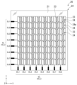
- FIG. It is a top view which shows the sensor main body of one Embodiment.
- It is a circuit diagram which shows a part of circuit structure of the same flexible sensor.
- It is a circuit diagram showing a circuit configuration of a sensor element in the same sensor body.
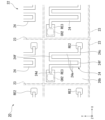
- It is sectional drawing which shows some sensor main bodies.
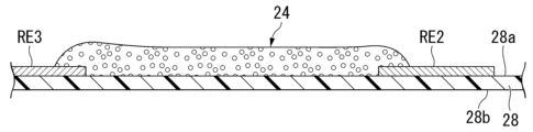
- FIG. 6 is a cross-sectional view showing a part of the sensor main body, and is a cross-sectional view taken along the line VI-VI in FIG. 5;
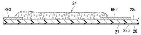
- FIG. 6 is a cross-sectional view showing a part of the sensor main body, taken along line VII-VII in FIG. 5; It is a figure which shows typically the structure of the control part of the same flexible sensor.
- FIG. 4 is a flow chart showing a method of manufacturing a flexible sensor according to one embodiment of the invention. It is sectional drawing explaining the resistance installation process of the manufacturing method of the same flexible sensor. It is sectional drawing explaining the adhesive layer installation process of the manufacturing method of the same flexible sensor. It is sectional drawing explaining the through-hole formation process of the manufacturing method of the same flexible sensor. It is sectional drawing explaining the adhesion
- the flexible sensor 10 of this embodiment is, for example, a strain sensor capable of measuring the strain of the object to be measured.
- the flexible sensor 10 includes a sensor body 20 , a wiring section 40 and a control section (measurement section) 30 .
- the sensor main body 20 is attached to a measurement object whose strain is to be measured.
- the sensor main body 20 has flexibility.
- the sensor main body 20 has a main substrate 21 and a sensor section 22, as shown in FIG.
- the main substrate 21 has portability.
- the flexibility of the main substrate 21 refers to the characteristic of being able to bend and elastically deform without breaking or breaking even when a force of about its own weight is applied. Flexibility also includes the property of being bent by a force equivalent to its own weight. Therefore, when the main substrate 21 is bent from a flat state by an external force within the range of elastic deformation, the main substrate 21 is composed of a base material having such a rigidity (Young's modulus) that it returns to the original flat state when the external force is removed. be done.
- the flexibility of the main substrate 21 may change depending on the material, size, thickness, environment such as temperature, etc. of the main substrate 21 . The same applies to the flexibility of the support substrate 28, which will be described later.
- the main substrate 21 preferably has electrical insulation.
- the base material of the main substrate 21 include polyacrylate, polycarbonate, polyurethane, polystyrene, cellulose polymer, polyolefin, polyamide, polyimide, polyester, polyphenylene, polyethylene, polyethylene terephthalate (PET), polyethylene naphthalate (PEN), polypropylene, Resin films such as ethylene vinyl copolymer and polyvinyl chloride, glass, sapphire, metal, cellulose nanofiber, etc. can be used as thin plates with a thickness of several tens of ⁇ m (micrometers) to several hundred ⁇ m. .
- the main substrate 21 is, for example, a square resin film.
- the shape of the main substrate 21 is not limited to a square shape, and may be a triangular shape, a rectangular shape, a rhombus shape, a polygonal shape with pentagons or more, a circular shape, an elliptical shape, or the like.
- the X-axis direction, the Y-axis direction, and the Z-axis direction are shown as appropriate with reference to the main substrate 21 in a state of not being deformed.
- the Z-axis direction indicates the thickness direction of the main substrate 21 .
- the X-axis direction indicates a direction parallel to one side of the square-shaped main substrate 21 .
- the Y-axis indicates a direction parallel to one side of the square-shaped main substrate 21 that extends in a direction different from the X-axis direction.
- the X-axis direction, the Y-axis direction, and the Z-axis direction are orthogonal to each other.
- the direction parallel to the Z-axis direction is called "thickness direction”.
- a direction parallel to the X-axis direction is called a “first direction”
- a direction parallel to the Y-axis direction is called a “second direction”.
- the positive side in the Z-axis direction (+Z side) is called the “upper side”
- the negative side in the Z-axis direction (-Z side) is called the “lower side”.
- the positive side (+X side) in the X-axis direction is called “one side in the first direction”
- the negative side (-X side) in the X-axis direction is called “the other side in the first direction”.
- the positive side (+Y side) in the Y-axis direction is called “second direction one side”
- the negative side (-Y side) in the Y-axis direction is called "second direction other side”.
- the sensor part 22 is a part that can detect the distortion of the object to be measured to which the sensor main body 20 is attached.
- the sensor unit 22 is provided on the upper (+Z side) surface of the main substrate 21 . As shown in FIGS. 2 and 3, the sensor unit 22 has a plurality of sensor elements 23, a plurality of scanning lines SL, a plurality of signal lines DL, and power supply electrodes (wiring for power supply) PL.
- the sensor section 22 is an active matrix type sensor section in which a plurality of sensor elements 23 are arranged in a matrix.
- the plurality of sensor elements 23 are arranged in a matrix along the first direction and the second direction.
- the sensor elements 23 are arranged in a matrix of 8 rows and 8 columns, and a total of 64 sensor elements 23 are provided.
- a plurality of sensor elements 23 are provided on the main substrate 21 .
- Each sensor element 23 has a transistor 25 and a variable resistance section 24, as shown in FIGS.
- the transistor 25 is provided at an end portion of the main substrate 21 on the support substrate 28 side, which will be described later.
- the transistor 25 is a field effect transistor (FET) having a gate electrode GE1, a source electrode SE1, and a drain electrode DE1.
- FET field effect transistor
- the transistor 25 is a thin film transistor (TFT).
- TFT thin film transistor
- the transistor 25 is, for example, an organic thin film transistor (OTFT).
- the transistor 25 has a P-type channel CA1, as shown in FIG.
- the material of channel CA1 is, for example, an organic semiconductor.
- organic semiconductors include copper phthalocyanine (CuPc), pentacene, rubrene, tetracene, 6,13-bis(triisopropylsilylethynyl)pentacene (TIPS pentacene), poly(3-hexylthiophene-2,5-diyl) ( P3HT) and the like can be used.
- Organic semiconductors that can be used as the material of the channel CA1 are not limited to the materials described above.
- the material of the channel CA1 may be an inorganic semiconductor.
- inorganic semiconductors that can be used include zinc oxide (ZnO), oxides containing ln, Ga, and Zn (lnGaZnO 4 : IGZO), amorphous silicon, low-temperature polysilicon, and the like.
- Inorganic semiconductors that can be used as the material of the channel CA1 are not limited to the above materials.
- the channel CA1 joins the source electrode SE1 and the drain electrode DE1.
- the transistor 25 is, for example, a bottom-gate and bottom-contact transistor.
- the source electrode SE1 and the drain electrode DE1 are arranged side by side in the first direction.
- the source electrode SE1 is positioned, for example, on one side (+X side) of the drain electrode DE1 in the first direction.
- the transistor 25 functions as an active matrix switching element that selects the variable resistance section 24 to be measured from among the variable resistance sections 24 that are two-dimensionally arranged at predetermined intervals in the first direction and the second direction. do.
- the variable resistance portion 24 is a portion whose resistance value changes according to strain (expansion and contraction due to bending of the main substrate 21 in the thickness direction).
- the variable resistance section 24 is in the form of a film formed on the upper (+Z side) surface of the support substrate 28 to be described later.
- the shape of the variable resistance section 24 is not limited.
- the variable resistance section 24 has a rectangular wave shape when viewed in a plane parallel to the XY plane.
- the variable resistance portion 24 has a plurality of extending portions 24e, a connecting portion 24f, and connecting portions 24c and 24d.
- the extending portion 24e extends in one direction.
- a plurality of extending portions 24e in one variable resistance portion 24 extend in the same direction and are arranged side by side at intervals in a direction orthogonal to the extending direction.
- the extension portions 24e extend in the second direction. That is, the direction in which the extension portion 24e extends is orthogonal to the direction in which the source electrode SE1 and the drain electrode DE1 are arranged.
- the extending portion 24e extends in the second direction in any variable resistance portion 24 of the sensor element 23. That is, in the plurality of sensor elements 23 included in the sensor section 22, the extending portions 24e of the variable resistance section 24 extend in the same direction.
- a plurality of extending portions extending in the same direction means that the plurality of extending portions extend in the same direction, and that the plurality of extending portions extend in substantially the same direction. Including cases where it extends to As an example, “a plurality of extending portions extend in substantially the same direction” includes a case where the direction in which a certain extending portion extends is deviated from the extending direction of another extending portion by about 10° or less.
- variable resistance portion 24 For example, three extending portions 24 e are provided for each variable resistance portion 24 .
- the plurality of extending portions 24e are arranged side by side at regular intervals in the first direction. The interval between the extending portions 24e is shorter than the length of the extending portions 24e. In this embodiment, the length of the extending portion 24e is the dimension of the extending portion 24e in the second direction.
- a plurality of extending portions are arranged at regular intervals means that the intervals between the extending portions are substantially the same, in addition to the case that the intervals between the extending portions are exactly the same. Including if there is.
- the distance between the extending portions is substantially the same includes the case where the difference between the distance between a pair of extending parts and the distance between another pair of extending parts is about 10% or less.
- the connecting portion 24f extends in the first direction and connects the ends of adjacent extending portions 24e.
- two connecting portions 24f are provided.
- One connecting portion 24f connects the end portions on the second direction one side (+Y side) of the center extending portion 24e and the extending portion 24e located on the first direction one side (+X side).
- the other connecting portion 24f connects the ends of the center extending portion 24e and the extending portion 24e located on the other side in the first direction ( ⁇ X side) on the other side in the second direction ( ⁇ Y side).
- the variable resistance portion 24 is formed in a rectangular wave shape by connecting the adjacent extending portions 24e to each other.
- the length of the connecting portion 24f is the same as the interval between the extending portions 24e and shorter than the length of the extending portions 24e. In this embodiment, the length of the connecting portion 24f is the dimension of the connecting portion 24f in the first direction.
- connection portion 24 c is one end portion of the variable resistance portion 24 .
- the connecting portion 24c extends in one direction in the first direction from the end portion on the other side in the second direction ( ⁇ Y side) of the extending portion 24e located on the one side in the first direction (+X side).
- the connection portion 24c is connected to the source electrode SE1 of the transistor 25.
- the variable resistance section 24 is thereby connected to the source electrode SE ⁇ b>1 of the transistor 25 . More specifically, the variable resistance section 24 is connected in series with the source electrode SE1.
- the connecting portion 24d is the other end of the variable resistance portion 24. As shown in FIG. 6, the connection portion 24d extends from the end portion of the extending portion 24e located on the other side in the first direction ( ⁇ X side) in the second direction (+Y side) to the other side in the first direction. there is The connection part 24d is connected to the power supply electrode PL, as shown in FIG. Thereby, the variable resistance section 24 is connected to the power supply electrode PL.
- the variable resistance section 24 has an insulator 24a and a plurality of conductive particles 24b dispersed in the insulator 24a, as exaggeratedly shown in FIG.
- the material of the insulator 24a is not particularly limited as long as it is an insulating material, and examples thereof include a resin material such as plastic and a polymer material such as rubber.
- the material of the insulator 24a is an energy curable resin.
- Energy-curable resins include, for example, thermosetting resins and photo-curable resins.
- the material of the conductive particles 24b is not particularly limited as long as it is a conductive material, and examples thereof include carbon (graphite) and metal.
- variable resistance section 24 When the variable resistance section 24 is distorted (expanded or contracted), the distance between the plurality of conductive particles 24b in the insulator 24a changes, and the conductivity of the variable resistance section 24 changes. As a result, the resistance value of the variable resistance section 24 changes according to the strain of itself (the variable resistance section 24). Specifically, for example, when the variable resistance section 24 is distorted in the direction of contraction, the distance between the conductive particles 24b in the insulator 24a is shortened, so that the contact interface between the conductive particles 24b is reduced. As a result, the resistance value of the variable resistance section 24 becomes smaller.
- variable resistance portion 24 when the variable resistance portion 24 is distorted in the direction in which it is stretched, the distance between the conductive particles 24b in the insulator 24a is increased, so that the contact interface between the conductive particles 24b is reduced and the variable resistance is increased.
- the resistance value of the portion 24 increases.
- variable resistance portion 24 when the variable resistance portion 24 is formed in a film shape on the support substrate 28 as in the present embodiment, when the sensor element 23 is bent downward ( ⁇ Z side) in a convex direction, the variable resistance The portion 24 is distorted in the contracted direction, and the resistance value of the variable resistance portion 24 decreases. On the other hand, when the sensor main body 20 is bent upwardly, the variable resistance section 24 is distorted in the direction of extension, and the resistance value of the variable resistance section 24 increases.
- the change in the resistance value of the variable resistance section 24 changes exponentially with respect to the rate of expansion and contraction of the variable resistance section 24 within a certain range of expansion and contraction of the variable resistance section 24 .
- the resistance value of the variable resistance section 24 does not change substantially. This is because the distance between the conductive particles 24b does not become any shorter and the resistance value does not become smaller.
- the resistance value of the variable resistance section 24 does not change substantially. This is because the distance between the conductive particles 24b becomes too long and the resistance value of the variable resistance section 24 does not increase any further.
- variable resistance section in this specification may be made using the sensor paint described in JP-A-2009-198482 and JP-A-2009-198483, for example.
- the “variable resistance section” in this specification may be made using, for example, the pressure-sensitive resistor paint described in Japanese Patent Application Laid-Open No. 60-127603.
- the "variable resistance part” may be made of a strain deformation resistance changing rubber described in Japanese Patent Application Laid-Open No. 62-12825, or a resistance ink for a strain gauge described in Japanese Patent Application Laid-Open No. 7-243805. , or an ink made of a polymeric material in which conductive particles (graphite) are dispersed, as described in JP-A-11-241903.
- the extending portion 24e, the connecting portion 24f, and the connecting portions 24c and 24d can be made of the same material.
- the portion necessary for strain (stretching) measurement is the extension portion 24e, the structure in which the resistance value changes as described above, that is, the structure having the insulator 24a and the conductive particles 24b is at least stretched.
- the part 24e should just have it. That is, the connecting portion 24f and the connecting portions 24c and 24d may not have the insulator 24a and the conductive particles 24b.
- the connecting portion 24f and connecting portions 24c and 24d may be thin films of conductive material such as gold, silver, copper, aluminum, nickel-phosphorus, and conductive polymer.
- the multiple scanning lines SL extend in the first direction.
- the multiple scanning lines SL are arranged at intervals along the second direction.
- eight scanning lines SL1 to SL8 are provided in this embodiment.
- a plurality of gate electrodes GE1 of transistors 25 are connected to each scanning line SL. More specifically, each of the scanning lines SL1 to SL8 is connected to the gate electrode GE1 of eight sensor elements 23 in each row among the sensor elements 23 arranged in eight rows and eight columns.
- the ends of the scanning lines SL1 to SL8 on the other side ( ⁇ X side) in the first direction are provided on the main substrate 21 as terminal portions.
- the multiple signal lines DL extend in the second direction.
- the multiple signal lines DL are arranged at intervals along the first direction.
- eight signal lines DL1 to DL8 are provided as the signal lines DL in this embodiment.
- a plurality of drain electrodes DE1 of transistors 25 are connected to each signal line DL. More specifically, each of the signal lines DL1 to DL8 is connected to the drain electrode DE1 of eight sensor elements 23 in each column among the sensor elements 23 arranged in 8 rows and 8 columns.
- the ends of the signal lines DL1 to DL8 on the other side ( ⁇ Y side) in the second direction are provided on the main substrate 21 as terminal portions.
- each of the scanning lines SL1 to SL8 is formed as the same layer on the surface of the main substrate 21 together with the gate electrode GE1 of each transistor 25, and an insulating film 26a laminated thereon.
- each of signal lines DL1 to DL8 is formed together with the drain electrode DE1 and the source electrode SE1 of each transistor 25. As shown in FIG.
- the signal line DL is connected to the fixed resistance section Ro provided in the control section 30 via the wiring section 40.
- fixed resistance units Ro1 to Ro8 are provided as the fixed resistance units Ro.
- Each fixed resistor section Ro1 to Ro8 is connected to each signal line DL1 to DL8.
- the fixed resistance units Ro1 to Ro8 are grounded to the ground GND provided in the control unit 30, respectively.
- the scanning lines SL1 to SL8 are collectively referred to as the scanning lines SLn.
- the signal lines DL1 to DL8 are collectively referred to as the signal line DLn, and the fixed resistance sections Ro1 to Ro8 are collectively referred to as the fixed resistance section Ron.
- n is an integer from 1 to 8 in each of the scanning line SLn, the signal line DLn, and the fixed resistance section Ron.
- the power supply electrode PL is an electrode to which a power supply potential having a value of Vcc is supplied from the control section 30 via the wiring section 40 .
- One end side of the variable resistance section 24 is connected to the power electrode PL.
- a source electrode SE ⁇ b>1 of a transistor 25 is connected to the other end of the variable resistance section 24 .
- each of the source electrodes SE1 of all the sensor elements 23 included in the sensor section 22 is individually connected to the power supply electrode PL via the variable resistance section 24 .
- each part of the sensor section 22 described above is formed in a film shape, and the sensor section 22 is configured by laminating a plurality of films on the main substrate 21 .
- Each part of the film-shaped sensor part 22 is formed by, for example, a wet method.
- the sensor section 22 includes an insulating film 26a, an insulating film 26b, an insulating film (coating member) 26c, an adhesive layer 27, a support substrate 28, a contact hole (wiring) CH1, and a contact hole CH2 in addition to the above-described parts. , relay electrodes RE1, RE2, and RE3.
- the material of the insulating films 26a, 26b, and 26c is, for example, an insulating inorganic material such as a silicon compound. 7, illustration of the insulating film 26b is omitted. In FIG. 6, illustration of the insulating film 26c is omitted.
- the scanning line SL, the signal line DL, the power supply electrode (wiring for power supply) PL, the gate electrode GE1, the source electrode SE1, the drain electrode DE1, the relay electrodes RE1, RE2, RE3, etc. are made of gold, silver, copper, aluminum, nickel-phosphorus. , consisting of a thin film of conductive material such as a conductive polymer.
- gate electrodes GE1, scanning lines SL, and insulating films 26a are formed on the upper surface of the main substrate 21.
- the insulating film 26a covers the gate electrode GE1 from above.
- the gate electrode GE1 and the scanning line SL are made by applying the same conductive material to the upper surface of the main substrate 21.
- the gate electrode GE1 and the scanning line SL can be formed by an inkjet method, a screen printing method, or the like using a conductive ink containing conductive nanoparticles of silver, gold, copper, or the like.
- the gate electrode GE1 and the scanning line SL are formed by an etching method of partially removing the metal thin film.
- the base material of the main substrate 21 is a sheet of a conductive material such as metal
- This insulating layer may be the same material as the insulating films 26a, 26b, and 26c, or may be a different material. Further, the insulating layer may be provided on the entire surface of the main substrate 21, or may be provided only on the regions on the main substrate 21 corresponding to the gate electrodes GE1 and the scanning lines SL.
- a source electrode SE1, a drain electrode DE1, a channel CA1, a signal line DL, a relay electrode RE1, and an insulating film 26b are formed on the upper surface of the insulating film 26a.
- the insulating film 26b covers the source electrode SE1, the drain electrode DE1, the channel CA1, the signal line DL, and the relay electrode RE1 from above.
- the source electrode SE1, the drain electrode DE1, the signal line DL, and the relay electrode RE1 are formed by applying the same conductive material (conductive ink, etc.) to the upper surface of the insulating film 26a, or by etching a metal thin film. It is made by
- the channel CA1 is made by applying an organic semiconductor material from above the source electrode SE1 and the drain electrode DE1.
- the source electrode SE1, the drain electrode DE1, and the channel CA1 are located above the gate electrode GE1.
- the relay electrode RE1 extends from the source electrode SE1 to one side (+X side) in the first direction.
- the adhesive layer 27 is arranged on the upper surface of the insulating film 26b.
- the adhesive layer 27 is a so-called double-sided tape.
- adhesive layers are provided on both sides of the base material.
- One adhesive layer of the adhesive layer 27 is attached to the insulating film 26b.
- the support substrate 28 has flexibility. At least the outer surface of the support substrate 28 is made of an electrically insulating material.
- the support substrate 28 is formed of a synthetic resin film having electrical insulation such as polyethylene terephthalate or polyimide.
- the thickness of the support substrate 28 is 50 ⁇ m.
- the support substrate may be made of stainless steel foil or the like with an insulating coating provided on all the outer surfaces and the inner surfaces of the through holes.
- a support substrate 28 is provided on the main substrate 21 . More specifically, the support substrate 28 is arranged on the upper surface of the adhesive layer 27 . The support substrate 28 is attached to the other adhesive layer of the adhesive layer 27 .
- a through hole H1 penetrating through the insulating film 26b, the adhesive layer 27, and the supporting substrate 28 is formed in the insulating film 26b, the adhesive layer 27, and the supporting substrate 28.
- Contact hole CH1 is arranged in through hole H1.
- a part of contact hole CH1 may be arranged in through hole H1.
- variable resistance section 24 is provided on a first surface 28 a of the support substrate 28 opposite to the main substrate 21 .
- the surface of the support substrate 28 opposite to the first surface 28a is referred to as a second surface 28b.
- the insulating film 26c covers the variable resistance section 24 and the relay electrodes RE2 and RE3 from above.
- the relay electrode RE2 and the relay electrode RE3 are made by applying the same conductive material to the upper surface (first surface 28a) of the support substrate 28.
- the conductive material forming the relay electrode RE2 and the relay electrode RE3 is, for example, the same as the conductive material forming the source electrode SE1, the drain electrode DE1, the signal line DL, and the relay electrode RE1.
- the relay electrode RE2 is connected to the relay electrode RE1 via a contact hole CH1 penetrating the insulating film 26b in the thickness direction.
- the connection portion 24c of the variable resistance portion 24 is connected to the relay electrode RE2. That is, in this embodiment, the variable resistance section 24 is connected to the source electrode SE1 of the transistor 25 via the relay electrode RE2, the contact hole CH1, and the relay electrode RE1.
- a contact hole CH ⁇ b>1 electrically connects the transistor 25 and the variable resistance section 24 .
- the relay electrode RE3 is connected to the connection portion 24d of the variable resistance portion 24. As shown in FIG.
- the insulating film 26c is provided on the first surface 28a of the support substrate 28. As shown in FIG. The insulating film 26c covers the variable resistance section 24, the relay electrodes RE2 and RE3, and the like. A power electrode PL is formed on the upper surface of the insulating film 26c.
- the power supply electrode PL is made, for example, by coating the upper surface of the insulating film 26c with the same conductive material as the material of each electrode described above, or by etching a metal thin film.
- the power electrode PL is connected to the relay electrode RE3 via a contact hole CH2 penetrating the insulating film 26c in the thickness direction.
- variable resistance section 24 is connected to the power supply electrode PL via the relay electrode RE2 and the contact hole CH2.
- source electrode SE1 is connected to the power electrode PL via the variable resistance section 24, the relay electrode RE2 and the contact hole CH2.
- an axis O1 along the first surface 28a of the support substrate 28 is defined.
- axis O1 is assumed to be along the second direction. Note that the axis may extend along the first direction.
- Axis O1 is preferably arranged on the lower surface of adhesive layer 27 .
- a geometric moment of inertia about the axis O1 of the main substrate 21 and the insulating films 26a and 26b as a whole is defined as I1 .
- a moment of inertia of area about the axis O1 of the adhesive layer 27, the support substrate 28, and the insulating film 26c is defined as I2 .
- the geometrical moment of inertia I1 and the geometrical moment of inertia I2 are equal to each other.
- the geometrical moment of inertia I 1 and the geometrical moment of inertia I 2 are equivalent to each other, meaning that the value of (I 1 /I 2 ) is 0.9 or more and 1.1 or less. is.
- the value of (I 1 /I 2 ) is preferably 0.95 or more and 1.05 or less.
- the configuration located below the lower surface of the adhesive layer 27 (hereinafter referred to as the lower configuration) as a whole, the geometrical moment of inertia about the axis O1, and the configuration located above the lower surface of the adhesive layer 27 (hereinafter referred to as the upper structure) be equal to each other.
- the lower structure and the upper structure are made of the same material as each other and are of the same thickness as each other.
- the wiring part 40 may be formed by flattening a plurality of wires parallel to each other and bundling them into a bond shape. Each wire line is flexible. As with the sensor body 20, the wiring part 40 is formed by forming a film-like wiring made of a conductive material such as gold, silver, copper, aluminum, nickel-phosphorus, or a conductive polymer on a substrate having abrasion resistance, and an insulating film. It may be coated with The wiring part 40 extends from the sensor body 20 .
- the wiring section 40 electrically connects the sensor main body 20 and the control section 30 . Although illustration is omitted, the wiring section 40 has a plurality of first wirings, a plurality of second wirings, power supply wirings, and ground GND (earth) wirings.
- the multiple first wirings are connected to multiple (eight) scanning lines SL, respectively, and extend to the control unit 30 .
- the plurality of second wirings are connected to the plurality (eight) of signal lines DL and extend to the control unit
- the controller 30 is connected to the sensor main body 20 via the wiring section 40 .
- the control unit 30 has a scanning line driving circuit 32, an 8-channel (8ch) AD converter circuit 33, and a microcomputer 31, as shown in FIG.
- a plurality of scanning lines SL 1 to SL 8 are connected to the scanning line driving circuit 32 .
- the scanning line drive circuit 32 sequentially outputs logic level (5V system or 3V system) pulse-sized scanning signals to any one of the plurality of scanning lines SL1 to SL8.
- the scanning signal is such that the gate potentials Vg1 to Vg8 applied to each of the scanning lines SL1 to SL8 by the level shifter 34 connected between each of the scanning lines SL1 to SL8 and the scanning line drive circuit 32 correspond to the characteristics of the transistor 25.
- the scanning signal from the scanning line drive circuit 32 is supplied to the scanning line SL via the level shifter 34 as the gate potential Vg
- the gate potential Vg is supplied to the gate electrode GE1 connected to the scanning line SL.
- the transistor 25 is turned on, and current flows from the source electrode SE1 to the drain electrode DE1 through the channel CA1.
- a voltage obtained by amplifying the output voltages Vo1 to Vo8 of the plurality of signal lines DL1 to DL8 by an amplifier 35 is applied to each channel of the 8ch AD converter circuit 33 .
- the resistance value of the variable resistance section 24 changes due to strain (expansion and contraction of the variable resistance section 24 due to bending of the main substrate 21). Therefore, the output voltage Vo, which is the divided potential applied to the fixed resistor section Ro, changes according to the change in the resistance value of the variable resistor section 24 .
- the resistance value of the variable resistance section 24 increases, the voltage value applied to the fixed resistance section Ro relatively decreases, so the output voltage Vo decreases.
- the resistance value of the variable resistance portion 24 decreases, the voltage value applied to the fixed resistance portion Ro relatively increases, so the output voltage Vo increases. Therefore, the change in the resistance value of the variable resistance section 24 can be obtained from the value of the output voltage Vo, and the distortion occurring in the sensor element 23 can be detected.
- variable resistance section 24 has a constant resistance value.
- the output voltage Vo (Vo1 to Vo8) generated by the resistance value of the variable resistance section 24 in the undistorted state is stored in advance in the memory of the microcomputer 31 as a digital value corresponding to the initial voltage value (initial value) in the undistorted state. stored in
- the output voltages Vo1 to Vo8 are each amplified by the amplifier 35 and input to the AD converter circuit 33 .
- the AD converter circuit 33 converts each of the input output voltages Vo1 to Vo8 into digital data.
- the AD converter circuit 33 outputs converted digital data to the microcomputer 31 based on a command from the microcomputer 31 .
- the AD converter circuit 33 incorporates, for example, an analog multiplexer circuit that selects one input signal out of eight channels of analog input signals.
- the AD converter circuit 33 sequentially converts the analog values of the output voltages Vo1 to Vo8 input from the signal lines DL1 to DL8 into digital values.
- the microcomputer 31 sends a command to the scanning line driving circuit 32 to sequentially supply gate potentials Vg1 to Vg8 to the plurality of scanning lines SL1 to SL8.
- the microcomputer 31 sends a command to the AD converter circuit 33 in accordance with the timing of supplying the gate potentials Vg1 to Vg8 to the scanning lines SL1 to SL8, and sequentially acquires the output voltages Vo1 to Vo8 from the signal lines DL1 to DL8. do.
- the output voltage Vo corresponding to all the sensor elements 23 included in the sensor section 22 can be obtained. Therefore, the change from the initial value of the resistance value of the variable resistance section 24 in each sensor element 23 can be obtained from the value of each output voltage Vo, and the distortion of each sensor element 23 can be detected.
- the microcomputer 31 outputs the acquired data to the display device 50 .
- the display device 50 displays, for example, information on distortion occurring in the sensor main body 20 on the display screen 51 .
- On the display screen 51 for example, square frames 52 corresponding to the 64 sensor elements 23 are displayed in an 8 ⁇ 8 matrix.
- the display device 50 changes the color of each frame 52 displayed on the display screen 51 according to the magnitude of the strain occurring in each sensor element 23, thereby displaying the distribution of strain occurring in the sensor body 20. It is possible.
- each square frame 52 arranged in an 8 ⁇ 8 matrix is displayed as a three-dimensional (3D) bar graph, and each of the 64 sensor elements 23 is in a non-distorted state.
- the height of the bar graph for each frame 52 may be adjusted to a constant value (initial height).
- the height of the bar graph in the frame 52 corresponding to the distorted portion is changed from the initial height according to the degree of distortion (curvature of that portion of the main substrate 21).
- FIG. 9 is a flow chart showing the manufacturing method S1 of this embodiment.
- the relay electrodes RE2 and RE3 are formed in advance by applying conductive ink or the like to the first surface 28a of the support substrate 28.
- the resistor installation step step S10 shown in FIG. 9
- the variable resistor section 24 is provided on the first surface 28a of the support substrate 28.
- the variable resistance section 24 is formed by screen printing or the like.
- the adhesive layer 27 is provided on the second surface 28b of the support substrate 28 in the adhesive layer providing step S12. More specifically, the other adhesive layer of the adhesive layer 27 is attached to the second surface 28 b of the support substrate 28 .
- the adhesive layer installation step S12 is performed after the resistance installation step S10. After the adhesive layer installation step S12 is completed, the process proceeds to step S14.
- a through-hole forming step S14 a through-hole H1 penetrating through the support substrate 28 and the adhesive layer 27 is formed.
- the through hole H1 may pass through the relay electrode RE2.
- the through holes H1 are formed with laser light.
- the through-hole forming step S14 is a step that is performed between the adhesive layer providing step S12 and the bonding step S16 described later. After the through-hole forming step S14 is completed, the process proceeds to step S16.
- the adhesive layer 27 is attached to the main substrate 21 in the bonding step S16. More specifically, one adhesive layer of the adhesive layer 27 is attached to the insulating film 26b. For example, a roller 60 is used to attach the adhesive layer 27 . Through holes H1 are formed in advance in the insulating film 26b at positions corresponding to the through holes H1 of the support substrate 28. As shown in FIG. For alignment between the main substrate 21 and the support substrate 28, for example, alignment marks or the like provided on both substrates 21 and 28 are used.
- the adhesion step S16 is a step performed after the adhesive layer installation step S12 and the through hole formation step S14. After the bonding step S16 is completed, the process proceeds to step S18. Next, as shown in FIG.
- the transistor 25 provided on the main substrate 21 and the variable resistance section 24 are electrically connected through the contact hole CH1 through the through hole H1.
- contact hole CH1 is formed by injecting silver paste into through hole H1 and heating the silver paste.
- the wiring step S18 is a step performed after the bonding step S16. After the wiring step S18 is completed, the process proceeds to step S20.
- a covering step S20 an insulating film 26c that covers the variable resistance section 24 is provided on the first surface 28a of the support substrate 28.
- the covering step S20 is finished and the power electrodes PL and the like are appropriately formed, all the steps of the manufacturing method S1 are finished, and the sensor body 20 is manufactured.
- the flexible sensor 10 is manufactured by connecting the wiring portion 40 and the control portion 30 to the sensor main body 20 .
- variable resistance part was formed directly on the main substrate by screen printing or the like.
- the main substrate is configured by laminating a plurality of layers (films). Therefore, when a screen mask or the like for screen printing is removed from the main board, force is applied to the main board, and the main board may be damaged, for example, by peeling off a plurality of layers.
- the variable resistance section 24 is provided on the first surface 28a of the support substrate 28 by screen printing or the like. . Since it is the support substrate 28 that receives force when removing the screen mask or the like, the main substrate 21 is less likely to be damaged. After that, the flexible sensor 10 is manufactured by, for example, attaching the support substrate 28 to the main substrate 21 . Therefore, the flexible sensor 10 can be manufactured while suppressing damage to the main substrate 21 .
- the resistance of the transistor changes according to the deformation. Since the flexible sensor 10 includes the support substrate 28 , the transistor 25 is positioned at the strain center of the flexible sensor 10 compared to when the flexible sensor 10 does not include the support substrate 28 . Therefore, when the flexible sensor 10 is bent, the transistor 25 is positioned near the strain center, and the transistor 25 is less likely to deform. Therefore, by measuring the resistance of the variable resistance section 24 using the transistor 25 when the flexible sensor 10 is bent, the resistance value of the variable resistance section 24 can be accurately measured.
- the flexible sensor 10 includes the support substrate 28 on which the variable resistance section 24 is provided, the variable resistance section 24 is farther from the strain center than when the flexible sensor 10 does not include the support substrate 28, and the flexible sensor 10 is The deformation of the variable resistance portion 24 when bent is increased. Thereby, bending (distortion) of the flexible sensor 10 can be measured with high accuracy.
- the flexible sensor 10 (sensor body 20) can be used to detect human motion.
- the flexible sensor 10 may be used by being directly attached to the human skin, or may be used by being attached to a wearable object such as clothes or shoes.
- the flexible sensor 10 may be attached to the back of the hand or the upper arm, and the finger movement may be indirectly detected based on the result of sensing the movement of the back of the hand or the upper arm.
- variable resistor section 24 is provided on the first surface 28a of the support substrate 28 by screen printing or the like in the resistor installation step S10. Since it is the support substrate 28 that receives force when removing the screen mask or the like, the main substrate 21 is less likely to be damaged.
- the adhesive layer 27 is provided on the second surface 28b of the support substrate 28 in the adhesive layer installation step S12. Then, in the bonding step S16, the adhesive layer 27 is attached to the main substrate 21, and the flexible sensor 10 is manufactured. Therefore, the flexible sensor 10 can be manufactured while suppressing damage to the main substrate 21 . In the manufacturing method S1, the same effects as those of the flexible sensor 10 can be obtained.
- the flexible sensor 10 has a contact hole CH1 that electrically connects the transistor 25 and the variable resistance section 24 and is arranged in the through hole H1. Further, in the manufacturing method S1, the through hole H1 is formed in the through hole forming step S14, and the transistor 25 and the variable resistance section 24 are electrically connected by the contact hole CH1 in the wiring step S18. As a result, the transistor 25 and the variable resistance section 24 can be electrically connected by the contact hole CH1 arranged in the through hole H1 penetrating the support substrate . If area moment of inertia I1 and area moment of inertia I2 are equal to each other, transistor 25 is located closer to the center of strain. Therefore, the transistor 25 becomes more difficult to deform, and the bending of the flexible sensor 10 can be measured with higher accuracy.
- the adhesive layer may be a layer of hot melt, UV (UltraViolet) curable resin, thermosetting resin, or the like.
- UV curable resin After the adhesive layer 27 is attached to the main substrate 21 in the adhesion step S16, the adhesive layer disposed between the insulating film 26b and the support substrate 28 is irradiated with ultraviolet rays. Irradiate.
- the flexible sensor 10 may not include the adhesive layer 27, the insulating film 26c, the contact holes CH1 and CH2, the wiring section 40, and the control section 30.
Landscapes
- Physics & Mathematics (AREA)
- General Physics & Mathematics (AREA)
- Measurement Of Length, Angles, Or The Like Using Electric Or Magnetic Means (AREA)
Priority Applications (4)
| Application Number | Priority Date | Filing Date | Title |
|---|---|---|---|
| JP2023576648A JPWO2023145220A1 (https=) | 2022-01-25 | 2022-11-22 | |
| CN202280089744.8A CN118575064A (zh) | 2022-01-25 | 2022-11-22 | 柔性传感器以及柔性传感器的制造方法 |
| KR1020247024154A KR20240127396A (ko) | 2022-01-25 | 2022-11-22 | 플렉서블 센서 및 플렉서블 센서의 제조 방법 |
| US18/779,202 US20240377180A1 (en) | 2022-01-25 | 2024-07-22 | Flexible sensor and method for manufacturing flexible sensor |
Applications Claiming Priority (2)
| Application Number | Priority Date | Filing Date | Title |
|---|---|---|---|
| JP2022009277 | 2022-01-25 | ||
| JP2022-009277 | 2022-01-25 |
Related Child Applications (1)
| Application Number | Title | Priority Date | Filing Date |
|---|---|---|---|
| US18/779,202 Continuation US20240377180A1 (en) | 2022-01-25 | 2024-07-22 | Flexible sensor and method for manufacturing flexible sensor |
Publications (1)
| Publication Number | Publication Date |
|---|---|
| WO2023145220A1 true WO2023145220A1 (ja) | 2023-08-03 |
Family
ID=87471416
Family Applications (1)
| Application Number | Title | Priority Date | Filing Date |
|---|---|---|---|
| PCT/JP2022/043157 Ceased WO2023145220A1 (ja) | 2022-01-25 | 2022-11-22 | フレキシブルセンサ及びフレキシブルセンサの製造方法 |
Country Status (5)
| Country | Link |
|---|---|
| US (1) | US20240377180A1 (https=) |
| JP (1) | JPWO2023145220A1 (https=) |
| KR (1) | KR20240127396A (https=) |
| CN (1) | CN118575064A (https=) |
| WO (1) | WO2023145220A1 (https=) |
Citations (5)
| Publication number | Priority date | Publication date | Assignee | Title |
|---|---|---|---|---|
| JP2016121974A (ja) * | 2014-12-25 | 2016-07-07 | 大日本印刷株式会社 | 圧力センサ |
| US20180247994A1 (en) * | 2017-02-28 | 2018-08-30 | Samsung Display Co., Ltd. | Display apparatus and method of manufacturing the same |
| JP2020085613A (ja) * | 2018-11-22 | 2020-06-04 | ムネカタインダストリアルマシナリー株式会社 | 歪みセンサアレイおよびその製造方法 |
| CN111883556A (zh) * | 2020-07-13 | 2020-11-03 | 浙江清华柔性电子技术研究院 | 柔性触觉传感器及其制备方法 |
| JP2021117032A (ja) * | 2020-01-23 | 2021-08-10 | 大日本印刷株式会社 | センサモジュール |
Family Cites Families (13)
| Publication number | Priority date | Publication date | Assignee | Title |
|---|---|---|---|---|
| JPH0758234B2 (ja) * | 1992-04-16 | 1995-06-21 | 株式会社エニックス | 半導体マトリクス型微細面圧分布センサ |
| JP3418561B2 (ja) | 1997-12-26 | 2003-06-23 | 豊明 木村 | 導電性粒子−高分子系による歪みセンサー |
| JP2003203523A (ja) * | 2002-01-08 | 2003-07-18 | Fujikura Ltd | 導電ペースト |
| US20050110767A1 (en) * | 2003-11-24 | 2005-05-26 | Elo Touchsystems, Inc. | Method of manufacturing touch sensor with switch tape strips |
| JP2005283329A (ja) * | 2004-03-30 | 2005-10-13 | Sanyo Electric Co Ltd | 感圧センサーパネルの製造方法 |
| JP2014228454A (ja) * | 2013-05-24 | 2014-12-08 | 株式会社フジクラ | 圧力センサ |
| JP6274029B2 (ja) * | 2014-06-18 | 2018-02-07 | 大日本印刷株式会社 | 圧力センサ装置およびその製造方法 |
| JP6198804B2 (ja) * | 2015-12-01 | 2017-09-20 | 日本写真印刷株式会社 | 多点計測用のひずみセンサとその製造方法 |
| JP6912170B2 (ja) * | 2016-09-14 | 2021-07-28 | エルジー ディスプレイ カンパニー リミテッド | 接触検知装置及びその駆動方法 |
| JP2018189583A (ja) * | 2017-05-10 | 2018-11-29 | 大日本印刷株式会社 | 圧力センサ装置 |
| US11243126B2 (en) * | 2017-07-27 | 2022-02-08 | Nextinput, Inc. | Wafer bonded piezoresistive and piezoelectric force sensor and related methods of manufacture |
| JP7567196B2 (ja) * | 2020-04-20 | 2024-10-16 | Toppanホールディングス株式会社 | 圧力センサおよび圧力センサアレイ |
| CN112284581B (zh) * | 2020-10-27 | 2022-04-15 | 湖北长江新型显示产业创新中心有限公司 | 一种传感器、显示面板及电子设备 |
-
2022
- 2022-11-22 WO PCT/JP2022/043157 patent/WO2023145220A1/ja not_active Ceased
- 2022-11-22 JP JP2023576648A patent/JPWO2023145220A1/ja active Pending
- 2022-11-22 KR KR1020247024154A patent/KR20240127396A/ko active Pending
- 2022-11-22 CN CN202280089744.8A patent/CN118575064A/zh active Pending
-
2024
- 2024-07-22 US US18/779,202 patent/US20240377180A1/en active Pending
Patent Citations (5)
| Publication number | Priority date | Publication date | Assignee | Title |
|---|---|---|---|---|
| JP2016121974A (ja) * | 2014-12-25 | 2016-07-07 | 大日本印刷株式会社 | 圧力センサ |
| US20180247994A1 (en) * | 2017-02-28 | 2018-08-30 | Samsung Display Co., Ltd. | Display apparatus and method of manufacturing the same |
| JP2020085613A (ja) * | 2018-11-22 | 2020-06-04 | ムネカタインダストリアルマシナリー株式会社 | 歪みセンサアレイおよびその製造方法 |
| JP2021117032A (ja) * | 2020-01-23 | 2021-08-10 | 大日本印刷株式会社 | センサモジュール |
| CN111883556A (zh) * | 2020-07-13 | 2020-11-03 | 浙江清华柔性电子技术研究院 | 柔性触觉传感器及其制备方法 |
Also Published As
| Publication number | Publication date |
|---|---|
| JPWO2023145220A1 (https=) | 2023-08-03 |
| KR20240127396A (ko) | 2024-08-22 |
| US20240377180A1 (en) | 2024-11-14 |
| CN118575064A (zh) | 2024-08-30 |
Similar Documents
| Publication | Publication Date | Title |
|---|---|---|
| US11860048B2 (en) | Capacitive and tactile sensors and related sensing methods | |
| US11079879B1 (en) | Flexible touch display device | |
| US8902597B2 (en) | Thin-film transistor forming substrate, semiconductor device, and electric apparatus | |
| KR20140143974A (ko) | 평판표시장치 | |
| JP2018005910A (ja) | タッチセンサー及びこれを含む表示装置 | |
| CN112993144B (zh) | 压电器件、压电传感器和可穿戴装置 | |
| US20110309415A1 (en) | Sensor using ferroelectric field-effect transistor | |
| CN104655000A (zh) | 一种柔性有源应变传感器结构及制备方法 | |
| US11322624B2 (en) | Detection apparatus, fabrication method thereof, array substrate, and display apparatus | |
| US20150340630A1 (en) | Flexible organic thin-film transistor and sensor having the same | |
| US10152152B2 (en) | Electret element and manufacturing method therefor, sensor, electronic circuit, and input device | |
| US20220324216A1 (en) | Lamination device | |
| CN110307777B (zh) | 一种压感面板及显示装置 | |
| WO2023145220A1 (ja) | フレキシブルセンサ及びフレキシブルセンサの製造方法 | |
| US8884266B2 (en) | Thin film transistor using a carbon nanotube as a channel and a display device including the same | |
| US20220082458A1 (en) | Flexible sensor | |
| Cosseddu et al. | Inkjet printed Organic Thin Film Transistors based tactile transducers for artificial robotic skin | |
| CN110243277B (zh) | 一种阵列基板、其驱动方法及显示装置 | |
| JP6860853B2 (ja) | 圧力センサ装置 | |
| JP5861756B2 (ja) | 曲げセンサー | |
| JP5625994B2 (ja) | 曲げセンサー | |
| CN113790666A (zh) | 应力感测组件和显示装置 | |
| JP2018189583A (ja) | 圧力センサ装置 | |
| TW201706580A (zh) | 壓力感測裝置、壓力感測方法及記憶媒體 | |
| CN114035710B (zh) | 外触发触控传感阵列及其制备方法 |
Legal Events
| Date | Code | Title | Description |
|---|---|---|---|
| 121 | Ep: the epo has been informed by wipo that ep was designated in this application |
Ref document number: 22924072 Country of ref document: EP Kind code of ref document: A1 |
|
| ENP | Entry into the national phase |
Ref document number: 20247024154 Country of ref document: KR Kind code of ref document: A |
|
| WWE | Wipo information: entry into national phase |
Ref document number: 202280089744.8 Country of ref document: CN |
|
| ENP | Entry into the national phase |
Ref document number: 2023576648 Country of ref document: JP Kind code of ref document: A |
|
| NENP | Non-entry into the national phase |
Ref country code: DE |
|
| 122 | Ep: pct application non-entry in european phase |
Ref document number: 22924072 Country of ref document: EP Kind code of ref document: A1 |