WO2023145101A1 - 検査装置および検査方法 - Google Patents
検査装置および検査方法 Download PDFInfo
- Publication number
- WO2023145101A1 WO2023145101A1 PCT/JP2022/016709 JP2022016709W WO2023145101A1 WO 2023145101 A1 WO2023145101 A1 WO 2023145101A1 JP 2022016709 W JP2022016709 W JP 2022016709W WO 2023145101 A1 WO2023145101 A1 WO 2023145101A1
- Authority
- WO
- WIPO (PCT)
- Prior art keywords
- inspection
- ray
- rays
- target
- inspection apparatus
- Prior art date
- Legal status (The legal status is an assumption and is not a legal conclusion. Google has not performed a legal analysis and makes no representation as to the accuracy of the status listed.)
- Ceased
Links
Images


Classifications
-
- G—PHYSICS
- G01—MEASURING; TESTING
- G01N—INVESTIGATING OR ANALYSING MATERIALS BY DETERMINING THEIR CHEMICAL OR PHYSICAL PROPERTIES
- G01N23/00—Investigating or analysing materials by the use of wave or particle radiation, e.g. X-rays or neutrons, not covered by groups G01N3/00 – G01N17/00, G01N21/00 or G01N22/00
- G01N23/02—Investigating or analysing materials by the use of wave or particle radiation, e.g. X-rays or neutrons, not covered by groups G01N3/00 – G01N17/00, G01N21/00 or G01N22/00 by transmitting the radiation through the material
- G01N23/06—Investigating or analysing materials by the use of wave or particle radiation, e.g. X-rays or neutrons, not covered by groups G01N3/00 – G01N17/00, G01N21/00 or G01N22/00 by transmitting the radiation through the material and measuring the absorption
- G01N23/18—Investigating the presence of flaws defects or foreign matter
-
- G—PHYSICS
- G01—MEASURING; TESTING
- G01N—INVESTIGATING OR ANALYSING MATERIALS BY DETERMINING THEIR CHEMICAL OR PHYSICAL PROPERTIES
- G01N23/00—Investigating or analysing materials by the use of wave or particle radiation, e.g. X-rays or neutrons, not covered by groups G01N3/00 – G01N17/00, G01N21/00 or G01N22/00
- G01N23/02—Investigating or analysing materials by the use of wave or particle radiation, e.g. X-rays or neutrons, not covered by groups G01N3/00 – G01N17/00, G01N21/00 or G01N22/00 by transmitting the radiation through the material
- G01N23/04—Investigating or analysing materials by the use of wave or particle radiation, e.g. X-rays or neutrons, not covered by groups G01N3/00 – G01N17/00, G01N21/00 or G01N22/00 by transmitting the radiation through the material and forming images of the material
-
- G—PHYSICS
- G01—MEASURING; TESTING
- G01N—INVESTIGATING OR ANALYSING MATERIALS BY DETERMINING THEIR CHEMICAL OR PHYSICAL PROPERTIES
- G01N23/00—Investigating or analysing materials by the use of wave or particle radiation, e.g. X-rays or neutrons, not covered by groups G01N3/00 – G01N17/00, G01N21/00 or G01N22/00
- G01N23/02—Investigating or analysing materials by the use of wave or particle radiation, e.g. X-rays or neutrons, not covered by groups G01N3/00 – G01N17/00, G01N21/00 or G01N22/00 by transmitting the radiation through the material
- G01N23/06—Investigating or analysing materials by the use of wave or particle radiation, e.g. X-rays or neutrons, not covered by groups G01N3/00 – G01N17/00, G01N21/00 or G01N22/00 by transmitting the radiation through the material and measuring the absorption
- G01N23/083—Investigating or analysing materials by the use of wave or particle radiation, e.g. X-rays or neutrons, not covered by groups G01N3/00 – G01N17/00, G01N21/00 or G01N22/00 by transmitting the radiation through the material and measuring the absorption the radiation being X-rays
-
- G—PHYSICS
- G01—MEASURING; TESTING
- G01N—INVESTIGATING OR ANALYSING MATERIALS BY DETERMINING THEIR CHEMICAL OR PHYSICAL PROPERTIES
- G01N23/00—Investigating or analysing materials by the use of wave or particle radiation, e.g. X-rays or neutrons, not covered by groups G01N3/00 – G01N17/00, G01N21/00 or G01N22/00
- G01N23/20—Investigating or analysing materials by the use of wave or particle radiation, e.g. X-rays or neutrons, not covered by groups G01N3/00 – G01N17/00, G01N21/00 or G01N22/00 by using diffraction of the radiation by the materials, e.g. for investigating crystal structure; by using scattering of the radiation by the materials, e.g. for investigating non-crystalline materials; by using reflection of the radiation by the materials
- G01N23/20008—Constructional details of analysers, e.g. characterised by X-ray source, detector or optical system; Accessories therefor; Preparing specimens therefor
-
- G—PHYSICS
- G01—MEASURING; TESTING
- G01N—INVESTIGATING OR ANALYSING MATERIALS BY DETERMINING THEIR CHEMICAL OR PHYSICAL PROPERTIES
- G01N23/00—Investigating or analysing materials by the use of wave or particle radiation, e.g. X-rays or neutrons, not covered by groups G01N3/00 – G01N17/00, G01N21/00 or G01N22/00
- G01N23/22—Investigating or analysing materials by the use of wave or particle radiation, e.g. X-rays or neutrons, not covered by groups G01N3/00 – G01N17/00, G01N21/00 or G01N22/00 by measuring secondary emission from the material
- G01N23/2206—Combination of two or more measurements, at least one measurement being that of secondary emission, e.g. combination of secondary electron [SE] measurement and back-scattered electron [BSE] measurement
-
- G—PHYSICS
- G01—MEASURING; TESTING
- G01N—INVESTIGATING OR ANALYSING MATERIALS BY DETERMINING THEIR CHEMICAL OR PHYSICAL PROPERTIES
- G01N23/00—Investigating or analysing materials by the use of wave or particle radiation, e.g. X-rays or neutrons, not covered by groups G01N3/00 – G01N17/00, G01N21/00 or G01N22/00
- G01N23/22—Investigating or analysing materials by the use of wave or particle radiation, e.g. X-rays or neutrons, not covered by groups G01N3/00 – G01N17/00, G01N21/00 or G01N22/00 by measuring secondary emission from the material
- G01N23/223—Investigating or analysing materials by the use of wave or particle radiation, e.g. X-rays or neutrons, not covered by groups G01N3/00 – G01N17/00, G01N21/00 or G01N22/00 by measuring secondary emission from the material by irradiating the sample with X-rays or gamma-rays and by measuring X-ray fluorescence
-
- G—PHYSICS
- G21—NUCLEAR PHYSICS; NUCLEAR ENGINEERING
- G21K—HANDLING OF PARTICLES OR IONISING RADIATION NOT OTHERWISE PROVIDED FOR; IRRADIATION DEVICES; GAMMA RAY OR X-RAY MICROSCOPES
- G21K7/00—Gamma- or X-ray microscopes
-
- H—ELECTRICITY
- H01—ELECTRIC ELEMENTS
- H01J—ELECTRIC DISCHARGE TUBES OR DISCHARGE LAMPS
- H01J35/00—X-ray tubes
- H01J35/02—Details
- H01J35/14—Arrangements for concentrating, focusing, or directing the cathode ray
- H01J35/153—Spot position control
-
- H—ELECTRICITY
- H01—ELECTRIC ELEMENTS
- H01J—ELECTRIC DISCHARGE TUBES OR DISCHARGE LAMPS
- H01J35/00—X-ray tubes
- H01J35/02—Details
- H01J35/16—Vessels; Containers; Shields associated therewith
- H01J35/18—Windows
- H01J35/186—Windows used as targets or X-ray converters
-
- G—PHYSICS
- G01—MEASURING; TESTING
- G01N—INVESTIGATING OR ANALYSING MATERIALS BY DETERMINING THEIR CHEMICAL OR PHYSICAL PROPERTIES
- G01N2223/00—Investigating materials by wave or particle radiation
- G01N2223/03—Investigating materials by wave or particle radiation by transmission
- G01N2223/04—Investigating materials by wave or particle radiation by transmission and measuring absorption
-
- G—PHYSICS
- G01—MEASURING; TESTING
- G01N—INVESTIGATING OR ANALYSING MATERIALS BY DETERMINING THEIR CHEMICAL OR PHYSICAL PROPERTIES
- G01N2223/00—Investigating materials by wave or particle radiation
- G01N2223/05—Investigating materials by wave or particle radiation by diffraction, scatter or reflection
- G01N2223/052—Investigating materials by wave or particle radiation by diffraction, scatter or reflection reflection
-
- G—PHYSICS
- G01—MEASURING; TESTING
- G01N—INVESTIGATING OR ANALYSING MATERIALS BY DETERMINING THEIR CHEMICAL OR PHYSICAL PROPERTIES
- G01N2223/00—Investigating materials by wave or particle radiation
- G01N2223/07—Investigating materials by wave or particle radiation secondary emission
- G01N2223/071—Investigating materials by wave or particle radiation secondary emission combination of measurements, at least 1 secondary emission
-
- G—PHYSICS
- G01—MEASURING; TESTING
- G01N—INVESTIGATING OR ANALYSING MATERIALS BY DETERMINING THEIR CHEMICAL OR PHYSICAL PROPERTIES
- G01N2223/00—Investigating materials by wave or particle radiation
- G01N2223/07—Investigating materials by wave or particle radiation secondary emission
- G01N2223/076—X-ray fluorescence
-
- G—PHYSICS
- G01—MEASURING; TESTING
- G01N—INVESTIGATING OR ANALYSING MATERIALS BY DETERMINING THEIR CHEMICAL OR PHYSICAL PROPERTIES
- G01N2223/00—Investigating materials by wave or particle radiation
- G01N2223/10—Different kinds of radiation or particles
- G01N2223/101—Different kinds of radiation or particles electromagnetic radiation
- G01N2223/1016—X-ray
-
- G—PHYSICS
- G01—MEASURING; TESTING
- G01N—INVESTIGATING OR ANALYSING MATERIALS BY DETERMINING THEIR CHEMICAL OR PHYSICAL PROPERTIES
- G01N2223/00—Investigating materials by wave or particle radiation
- G01N2223/20—Sources of radiation
-
- G—PHYSICS
- G01—MEASURING; TESTING
- G01N—INVESTIGATING OR ANALYSING MATERIALS BY DETERMINING THEIR CHEMICAL OR PHYSICAL PROPERTIES
- G01N2223/00—Investigating materials by wave or particle radiation
- G01N2223/20—Sources of radiation
- G01N2223/204—Sources of radiation source created from radiated target
-
- G—PHYSICS
- G01—MEASURING; TESTING
- G01N—INVESTIGATING OR ANALYSING MATERIALS BY DETERMINING THEIR CHEMICAL OR PHYSICAL PROPERTIES
- G01N2223/00—Investigating materials by wave or particle radiation
- G01N2223/30—Accessories, mechanical or electrical features
- G01N2223/32—Accessories, mechanical or electrical features adjustments of elements during operation
-
- G—PHYSICS
- G01—MEASURING; TESTING
- G01N—INVESTIGATING OR ANALYSING MATERIALS BY DETERMINING THEIR CHEMICAL OR PHYSICAL PROPERTIES
- G01N2223/00—Investigating materials by wave or particle radiation
- G01N2223/60—Specific applications or type of materials
- G01N2223/643—Specific applications or type of materials object on conveyor
-
- G—PHYSICS
- G01—MEASURING; TESTING
- G01N—INVESTIGATING OR ANALYSING MATERIALS BY DETERMINING THEIR CHEMICAL OR PHYSICAL PROPERTIES
- G01N2223/00—Investigating materials by wave or particle radiation
- G01N2223/60—Specific applications or type of materials
- G01N2223/652—Specific applications or type of materials impurities, foreign matter, trace amounts
Definitions
- the present invention relates to an inspection device and an inspection method.
- Japanese Patent Application Laid-Open No. 2009-236622 discloses a method for detecting fluorescent X-rays generated from a sample by focusing an electron beam on a target for generating X-rays with an objective lens and irradiating the sample with the X-rays generated from the target.
- a high-resolution X-ray microscope with a fluorescent X-ray analysis function is described, which includes a detector and an analysis unit for analyzing fluorescent X-rays from the detection result of the detector.
- Japanese Patent Application Laid-Open No. 2009-236622 describes incorporating all or part of the detector into the magnetic circuit of the objective lens.
- the vibration of the foreign matter may break the separator that maintains the insulation inside the battery after the battery is shipped. In such cases, the battery may become short-circuited and catch fire or explode.
- Fluorescent X-ray method also known as XRF
- oblique incident fluorescent X-ray method also known as TXRF
- TXRF oblique incident fluorescent X-ray method
- the present invention provides an advantageous technique for detecting foreign matter existing on the surface to be inspected with high sensitivity.
- One aspect of the present invention relates to an inspection apparatus for inspecting a surface to be inspected arranged on an inspection surface, the inspection apparatus including an X-ray generator that generates X-rays by being irradiated with an electron beam. and an X-ray generating tube that emits X-rays toward the inspection surface; an X-ray detector that detects the totally reflected X-rays.
- Another aspect of the present invention relates to an inspection method for inspecting a surface to be inspected arranged on an inspection surface, the inspection method radiating X-rays toward the inspection surface and generating X-rays existing on the surface to be inspected.
- FIG. 2 is a diagram schematically showing a configuration example of an X-ray generating tube
- FIG. 3 is a schematic diagram enlarging a part of the inspection apparatus in FIG. 2
- FIG. 5 is a schematic diagram enlarging a part of the inspection apparatus in FIG. 4
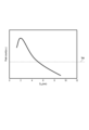
- FIG. 4 is a diagram illustrating the relationship between the distance D xs (horizontal axis) and the number of foreign particles detected by the X-ray detector (vertical axis);
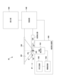
- FIG. 1 schematically shows the configuration of the inspection apparatus IA of the embodiment.
- the inspection apparatus IA can be configured, for example, as an inspection apparatus that inspects the inspection target surface TS arranged on the inspection surface IP.
- the inspection plane IP is a plane on which the inspection target plane TS is to be arranged
- the inspection target plane TS is one plane of the inspection target IT.
- the inspection apparatus IA may comprise an X-ray generator tube 101 .
- the X-ray generating tube 101 has a target (not shown) including an X-ray generator XG that generates X-rays by being irradiated with an electron beam, and emits X-rays XR toward the inspection plane IP.
- the foreign object FS irradiated with the X-rays XR from the X-ray generating part XG generates X-rays corresponding to the substances forming the foreign object FS, and such X-rays are also called fluorescent X-rays or characteristic X-rays.
- Part of the X-rays generated by the foreign matter FS irradiated with the X-rays XR is totally reflected by the inspection target surface TS.
- the X-rays emitted from the foreign object FS and totally reflected by the surface TS to be inspected are shown as X-rays XF.
- Inspection apparatus IA may comprise an X-ray detector 120 .
- Inspection apparatus IA may further include a processor that performs processing for detecting foreign matter FS based on the output from X-ray detector 120 .
- the processor may further perform processing to identify the material that constitutes the foreign object FS based on the output from the X-ray detector 120 .
- the processor can be implemented, for example, by a control unit that controls the operation of inspection apparatus IA.
- FIG. 2 shows a more specific configuration example of the inspection apparatus IA shown in FIG.
- the inspection apparatus IA can include an X-ray generator 100 , an X-ray detector 120 and a controller 140 .
- the X-ray generator 100 can include an X-ray generator tube 101 and a drive circuit 103 that drives the X-ray generator tube 101 .
- the X-ray generator 100 can further include a booster circuit 102 that supplies a boosted voltage to the drive circuit 103 .
- the X-ray generator 100 further includes a storage container (not shown) that stores the X-ray generation tube 101, the drive circuit 103, and the booster circuit 102, and the storage container can be filled with an insulating fluid such as insulating oil. .
- Controller 140 may be configured to control X-ray generator 100 and X-ray detector 120 .
- the controller 140 may also include the functionality of the processor described above. More specifically, control unit 140 can perform processing for detecting foreign matter FS based on the output from X-ray detector 120 . In addition, the control unit 140 can further perform a process of identifying substances that constitute the foreign matter FS based on the output from the X-ray detector 120 .
- the control unit 140 is, for example, PLD (abbreviation of Programmable Logic Device) such as FPGA (abbreviation of Field Programmable Gate Array), or ASIC (abbreviation of Application Specific Integrated Circuit), or a general-purpose device in which a program is incorporated. or a dedicated computer, or a combination of all or part of these.
- PLD abbreviation of Programmable Logic Device
- FPGA abbreviation of Field Programmable Gate Array
- ASIC abbreviation of Application Specific Integrated Circuit
- the inspection apparatus IA may further include an X-ray detection panel 130 that detects X-rays emitted from the X-ray generator XG and transmitted through the inspection object IT having the inspection object surface TS. Based on the output from the X-ray detection panel 130, the control unit 140 generates an image of X-rays transmitted through the inspection object IT (transmission image of the inspection object IT), and based on the image, detects the surface of the inspection object. It can be configured to detect a foreign object FS present in the TS. By using the X-ray detection panel 130, it is also possible to detect foreign matter present inside the inspection object IT and foreign matter existing on the surface opposite to the inspection object surface TS.
- the controller 140 can be configured to detect the presence of a foreign object FS as well as the position and/or size of the foreign object FS.
- the X-ray detection panel 130 in addition to the X-ray detector 120, the foreign matter FS that cannot be detected by the X-ray detector 120 can be detected by the X-ray detection panel 130, so the accuracy of detecting the foreign matter FS is improved.
- the inspection apparatus IA which acquires a transmission image and detects foreign matter using X-rays emitted from one X-ray generating tube, is composed of two devices that separately acquire a transmission image and detect foreign matter. It is advantageous in terms of miniaturization and cost reduction compared to systems with
- the inspection apparatus IA may further include a display unit 150, and the control unit 140 causes the display unit 150 to display information indicating the constituent materials of the foreign matter FS identified based on the output of the X-ray detector 120. can be configured.
- the control unit 140 can also be configured to cause the display unit 150 to display a transmitted image of the inspection object IT generated based on the output from the X-ray detection panel 130 .
- the control unit 140 can also be configured to cause the display unit 150 to display information indicating the position and/or size of the detected foreign object based on the output from the X-ray detection panel 130 .
- the control unit 140 may be configured as a single unit, or may be configured by being divided into a plurality of units.
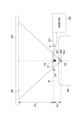
- the X-ray generating tube 101 can include an electron gun EG, an anode 93 having a target 933 including an X-ray generating portion XG that generates X-rays by being struck by electrons from the electron gun EG, and an insulating tube 92 .
- an anode 93 is arranged so as to block one of the two open ends of the insulating tube 92, and a block containing the electron gun EG is arranged so as to block the other of the two open ends of the insulating tube 92.
- a member 91 may be arranged.
- a deflector 94 that deflects the flow of electrons (electron beam) from the electron gun EG may be arranged outside the insulating tube 92 .
- the X-ray generating tube 101 shown in FIG. 3 is a closed transmission type X-ray generating tube in which the inner space of the insulating tube 92 is maintained in a vacuum state and X-rays pass through a target 933 and a target holding plate 932, which will be described later.
- a non-sealed open type or a non-transmissive reflecting type X-ray generating tube may be employed as the X-ray generating tube 101.
- the deflector 94 can be arranged outside the X-ray generating tube 101 .
- the deflector 94 can be provided between the anode 93 and the cathode (not shown).
- the deflector 94 is provided between the electron gun EG and the target 933 .
- a virtual plane 97 that intersects the deflector 94 can be positioned in a space sandwiched between a virtual plane 95 contacting the tip of the electron gun EG and a virtual plane 96 contacting a portion of the target 933 .
- a virtual plane 95 , a virtual plane 96 , and a virtual plane 97 are planes perpendicular to the axis AX of the X-ray generating tube 101 .
- the anode 93 can include a target 933 , a target holding plate 932 holding the target 933 , and an electrode 931 holding the target holding plate 932 .
- the electrode 931 is electrically connected to the target 933 and can apply an electric potential to the target 933 .
- the target 933 generates X-rays when electrons (electron beams) emitted from the electron gun EG collide with the target 933 .
- the X-ray generator XG is a portion of the surface of the target 933 that is hit by electrons (electron beams).
- the X-rays generated by the X-ray generator XG pass through the target holding plate 932 and are emitted to the outside of the X-ray generating tube 101 .
- Anode 93 may be maintained at, for example, ground potential, but may be maintained at other potentials.
- the target 933 is made of a metal material.
- the target 933 is desirably made of a material with a high melting point, such as tungsten, tantalum, molybdenum, or the like, which contributes to the improvement of X-ray generation efficiency.
- the target holding plate 932 can be made of a material that is highly transparent to X-rays, such as beryllium or diamond.
- the target holding plate 932 is desirably made of diamond, so that the strength of the target holding plate 932 can be maintained and the thickness can be reduced. The distance to the line generator XG) can be shortened. It is desirable that the thickness of the target holding plate 932 is thin.
- the thickness of the target holding plate 932 is desirably 4 mm or less, and more desirably 2 mm or less, 1 mm or less, or 0.3 mm or less.
- the thicknesses of these target holding plates 932 can be set with reference to the distance from the X-ray generation unit XG to the inspection surface IP, which is necessary for identifying elements contained in foreign matter, which will be described later.
- the target holding plate 932 is as thin as possible. From the viewpoint of strength, etc., it is desirable that the thickness is large. Therefore, it is desirable to use an optimum target holding plate 932 thickness.
- FIG. 3 is not intended to show the relationship between the thickness of the target 933 and the thickness of the target holding plate 932 .
- the thickness of the target 933 may be several ⁇ m
- the thickness of the target holding plate 932 may be several hundred ⁇ m.
- FIG. 4 is a schematic diagram enlarging a part of the inspection apparatus IA in FIG.
- a foreign matter FS may exist on the inspection target surface TS.
- the X-ray capturing unit 121 of the X-ray detector 120 arranged to detect the X-rays (characteristic X-rays) XF is irradiated with the X-rays XR from the X-ray generating unit XG, and the inspection object IT Fluorescent X-rays that can be generated by itself hardly enter. Therefore, the ratio of the fluorescent X-rays emitted from the inspection object IT itself and detected by the X-ray detector 120 to the X-rays (characteristic X-rays) XF emitted from the foreign object FS and detected by the X-ray detector 120 is extremely small. can do.
- the X-ray detector 120 may be a silicon drift detector (SDD), a CdTe detector or a CdZnTe detector.
- X-ray detector 120 may be an energy dispersive detector. If the X-ray detector 120 is an energy dispersive detector, the controller (or processor) 140 can determine the substances or elements that make up the foreign matter FS from the energy dispersive element profile (count value for each energy). can.
- Commercially available software may be installed in the controller (or processor) 140 to determine the substances or elements that make up the foreign matter FS. Examples of such software include AMETEK's "XRS-FP Quantitative XRF Analysis Software" and Unique's software.
- the incident angle of the fluorescent X-rays from the foreign matter FS to the inspection target surface TS must be the total reflection critical angle ⁇ c or less.
- ⁇ c Critical angle of total reflection
- r e Classical radius of electron (2.818 ⁇ 10 ⁇ 15 m)
- N 0 Avogadro's number
- ⁇ X-ray wavelength
- ⁇ Density (g/cm 3 )
- Mi xi: atomic number, atomic weight and atomic number ratio (molar ratio) of the i-th atom
- f′ i atomic scattering factor of i-th atom (anomalous dispersion term)
- the critical angle of total reflection when the surface TS to be inspected is metal is approximately 1° or less. In many cases, the critical angle of reflection is different from the theoretical value.
- the inspection object surface TS When the inspection object surface TS is irradiated with X-rays XR and the total reflection condition is satisfied, the inspection object surface TS and the characteristic X-ray XF emitted from the foreign matter FS and totally reflected by the inspection object surface TS It was confirmed through experiments that the angle between and (the critical angle for total reflection) is 5° or less.
- the angle between and the critical angle for total reflection
- the position where the radiation from the foreign matter FS is totally reflected by the inspection target surface TS is , the positions at which the X-rays XR from the X-ray generator XG are incident on the inspection surface IP.
- the position where the foreign object FS radiates and is totally reflected by the inspection object surface TS can be regarded as a position where the X-ray XR from the X-ray generator XG is perpendicularly incident on the inspection plane IP.
- the critical angle of total reflection is 5° or less
- the angle ⁇ formed with the plane IP can be 5° or less, preferably 2° or less, and more preferably 1° or less.
- the smaller the angle ⁇ the more the fluorescent X-rays emitted from the inspection object IT itself and detected by the X-ray detector 120 relative to the X-rays (characteristic X-rays) XF emitted from the foreign object FS and detected by the X-ray detector 120. You can reduce the ratio.
- the X-ray detector 120 can be arranged at a position where the extended plane of the inspection plane IP intersects the X-ray detector 120 .
- the X-ray capturing section 121 can include a window section 122 that transmits X-rays XF, as schematically shown in FIG.
- the window 122 can have a diameter of several mm and a thickness of several hundred ⁇ m, for example.
- the window part 122 can be made of beryllium or the like, for example.
- the inspection apparatus IA has a virtual plane connecting the position where the X-ray XR from the X-ray generator XG is incident on the inspection surface IP and the X-ray capturing section 121 of the X-ray detector 120 .
- a slit member 125 having slits (openings) above the line may be provided.
- the size of the slit provided in the slit member 125 and the arrangement position of the X-ray detector 120 are determined according to the range of the surface to be inspected TS hit by the X-ray XR, the material that can constitute the surface to be inspected TS and the foreign matter FS, and the like. can be As schematically shown in FIG. 7, foreign matter FS1 and FS3 are present at both ends of width Y on inspection target surface TS with which X-ray XR hits, and distance Z from the center of width Y to X-ray capturing unit 121 is is the same length as the width Y.
- the lower limit of the width Ws of the slit is Y ⁇ tan ⁇
- the distance X2 between the center of the X-ray capturing portion 121 and the inspection surface IP is also Y ⁇ tan ⁇ . It is possible to detect all foreign objects within the hit range.
- FIG. 6 shows experimentally obtained results of the relationship between the distance D xs (horizontal axis) and the count number (vertical axis) of the foreign matter FS detected by the X-ray detector 120 .
- the count number is the total count number (peak count) of the energy corresponding to the position of the fluorescent X-ray (for example, the K ⁇ ray of Ni) emitted from the specific element contained in the foreign matter per certain time.
- the distance Dxs from the X-ray generation unit XG to the inspection surface IP is preferably 5 mm or less, more preferably 4 mm or less, and 3 mm or less. It is even more desirable to have As the X-ray generating tube 101, for example, transparent closed microfocus X-ray sources manufactured by Canon Anelva, specifically G series, more specifically G-511 series and G-311 series are useful.
- the distance D sf from the inspection plane IP to the X-ray detection panel 130 needs to be sufficiently larger than D xs . .
- D sf /D xs is desirably 20 or more, and more desirably 200 or more.
- the inspection device IA is useful, for example, in the production process of lithium-ion batteries to detect relics attached to the material, but this is only an example and it is also useful for other purposes.
- the inspection device IA may be used, for example, to measure and analyze airborne particles such as PM2.5 that affect the environment and health.
- the inspection apparatus IA is used to measure the number and size of particles as well as configure particles. Since it is possible to simultaneously identify the substances or elements that are affected, more advanced environmental and health measures can be taken.
- X-rays are emitted toward an inspection surface IP (inspection target surface TS), and X-rays XF emitted from a foreign substance FS present on the inspection target surface TS and totally reflected by the inspection target surface TS are converted into X-rays.
- It may include an x-ray detection step for detection by the detector 120 and a processing step for processing the output of the x-ray detector 120 .
- the processing step may include a step of detecting foreign matter FS and/or a step of identifying substances that constitute foreign matter FS.
- the inspection method can further include a step of detecting, with the X-ray detection panel 130, X-rays transmitted through the inspection object IT having the inspection object surface TS.
- the output of the x-ray detection panel 130 may be processed.
- the processing steps may include detecting the presence of the foreign object FS and the position of the foreign object FS based on the output of the X-ray detection panel 130 .
- the processing may include detecting the presence of the foreign object FS, the location of the foreign object FS, and the size of the foreign object FS based on the output of the x-ray detection panel 130 .
Landscapes
- Chemical & Material Sciences (AREA)
- Health & Medical Sciences (AREA)
- Physics & Mathematics (AREA)
- Biochemistry (AREA)
- Life Sciences & Earth Sciences (AREA)
- Analytical Chemistry (AREA)
- General Health & Medical Sciences (AREA)
- General Physics & Mathematics (AREA)
- Immunology (AREA)
- Pathology (AREA)
- Crystallography & Structural Chemistry (AREA)
- Toxicology (AREA)
- High Energy & Nuclear Physics (AREA)
- General Engineering & Computer Science (AREA)
- Engineering & Computer Science (AREA)
- Analysing Materials By The Use Of Radiation (AREA)
Priority Applications (4)
| Application Number | Priority Date | Filing Date | Title |
|---|---|---|---|
| CN202280090523.2A CN118661094A (zh) | 2022-01-31 | 2022-03-31 | 检查装置以及检查方法 |
| KR1020247028367A KR20240141192A (ko) | 2022-01-31 | 2022-03-31 | 검사 장치 및 검사 방법 |
| EP22923964.5A EP4474800A4 (en) | 2022-01-31 | 2022-03-31 | INSPECTION DEVICE AND INSPECTION PROCEDURE |
| US18/350,054 US11927554B2 (en) | 2022-01-31 | 2023-07-11 | Inspection apparatus and inspection method |
Applications Claiming Priority (2)
| Application Number | Priority Date | Filing Date | Title |
|---|---|---|---|
| JP2022-013653 | 2022-01-31 | ||
| JP2022013653 | 2022-01-31 |
Related Child Applications (1)
| Application Number | Title | Priority Date | Filing Date |
|---|---|---|---|
| US18/350,054 Continuation US11927554B2 (en) | 2022-01-31 | 2023-07-11 | Inspection apparatus and inspection method |
Publications (1)
| Publication Number | Publication Date |
|---|---|
| WO2023145101A1 true WO2023145101A1 (ja) | 2023-08-03 |
Family
ID=87471017
Family Applications (5)
| Application Number | Title | Priority Date | Filing Date |
|---|---|---|---|
| PCT/JP2022/016709 Ceased WO2023145101A1 (ja) | 2022-01-31 | 2022-03-31 | 検査装置および検査方法 |
| PCT/JP2022/043908 Ceased WO2023145238A1 (ja) | 2022-01-31 | 2022-11-29 | 検査装置および検査方法 |
| PCT/JP2022/043906 Ceased WO2023145236A1 (ja) | 2022-01-31 | 2022-11-29 | 異物検出および蛍光x線による同定装置 |
| PCT/JP2022/043905 Ceased WO2023145235A1 (ja) | 2022-01-31 | 2022-11-29 | 検査装置および検査方法 |
| PCT/JP2022/043907 Ceased WO2023145237A1 (ja) | 2022-01-31 | 2022-11-29 | 検査装置および検査方法 |
Family Applications After (4)
| Application Number | Title | Priority Date | Filing Date |
|---|---|---|---|
| PCT/JP2022/043908 Ceased WO2023145238A1 (ja) | 2022-01-31 | 2022-11-29 | 検査装置および検査方法 |
| PCT/JP2022/043906 Ceased WO2023145236A1 (ja) | 2022-01-31 | 2022-11-29 | 異物検出および蛍光x線による同定装置 |
| PCT/JP2022/043905 Ceased WO2023145235A1 (ja) | 2022-01-31 | 2022-11-29 | 検査装置および検査方法 |
| PCT/JP2022/043907 Ceased WO2023145237A1 (ja) | 2022-01-31 | 2022-11-29 | 検査装置および検査方法 |
Country Status (7)
| Country | Link |
|---|---|
| US (6) | US11921059B2 (https=) |
| EP (5) | EP4474800A4 (https=) |
| JP (6) | JP7667882B2 (https=) |
| KR (5) | KR20240141192A (https=) |
| CN (5) | CN118661094A (https=) |
| TW (6) | TW202433050A (https=) |
| WO (5) | WO2023145101A1 (https=) |
Families Citing this family (1)
| Publication number | Priority date | Publication date | Assignee | Title |
|---|---|---|---|---|
| WO2023145101A1 (ja) * | 2022-01-31 | 2023-08-03 | キヤノンアネルバ株式会社 | 検査装置および検査方法 |
Citations (6)
| Publication number | Priority date | Publication date | Assignee | Title |
|---|---|---|---|---|
| US6829327B1 (en) * | 2000-09-22 | 2004-12-07 | X-Ray Optical Systems, Inc. | Total-reflection x-ray fluorescence apparatus and method using a doubly-curved optic |
| JP2005292077A (ja) * | 2004-04-05 | 2005-10-20 | Fuji Electric Holdings Co Ltd | X線顕微鏡装置 |
| JP2009236622A (ja) | 2008-03-26 | 2009-10-15 | Tohken Co Ltd | 蛍光x線分析機能付き高分解能x線顕微装置 |
| JP2013044644A (ja) * | 2011-08-24 | 2013-03-04 | Fujitsu Ltd | 半導体装置の検査方法及び半導体装置の製造方法 |
| WO2017104659A1 (ja) * | 2015-12-15 | 2017-06-22 | 株式会社堀場製作所 | X線管、及び、x線分析装置 |
| JP2022013653A (ja) | 2020-07-03 | 2022-01-18 | ミン マイケル ホー,ホイ | 関節支持装置 |
Family Cites Families (49)
| Publication number | Priority date | Publication date | Assignee | Title |
|---|---|---|---|---|
| JPH01244344A (ja) * | 1988-03-25 | 1989-09-28 | Hitachi Ltd | X線吸収スペクトル測定装置 |
| JPH07119717B2 (ja) * | 1989-12-12 | 1995-12-20 | シャープ株式会社 | 半導体材料評価装置 |
| JPH0534131A (ja) * | 1991-08-05 | 1993-02-09 | Fujitsu Ltd | 画像処理方法及び画像処理装置 |
| JPH05346411A (ja) * | 1992-04-16 | 1993-12-27 | Rigaku Denki Kogyo Kk | 蛍光x線分析装置 |
| EP0697109B1 (en) * | 1994-03-02 | 1999-07-14 | Koninklijke Philips Electronics N.V. | X-ray spectrometer with a grazing take-off angle |
| JP3165615B2 (ja) * | 1995-03-17 | 2001-05-14 | 財団法人国際超電導産業技術研究センター | 表面元素分析方法及び装置 |
| KR100233312B1 (ko) | 1995-08-09 | 1999-12-01 | 야마모토 카즈모토 | 전반사 형광 x선 분석 장치 및 방법 |
| US5742658A (en) * | 1996-05-23 | 1998-04-21 | Advanced Micro Devices, Inc. | Apparatus and method for determining the elemental compositions and relative locations of particles on the surface of a semiconductor wafer |
| JPH09318565A (ja) * | 1996-05-24 | 1997-12-12 | Rigaku Ind Co | X線分析方法および装置 |
| JP2984232B2 (ja) * | 1996-10-25 | 1999-11-29 | 株式会社テクノス研究所 | X線分析装置およびx線照射角設定方法 |
| US6005915A (en) | 1997-11-07 | 1999-12-21 | Advanced Micro Devices, Inc. | Apparatus and method for measuring the roughness of a target material surface based upon the scattering of incident X-ray photons |
| US6108398A (en) | 1998-07-13 | 2000-08-22 | Jordan Valley Applied Radiation Ltd. | X-ray microfluorescence analyzer |
| JP2000055841A (ja) * | 1998-08-13 | 2000-02-25 | Fujitsu Ltd | X線分析方法 |
| DE19934987B4 (de) | 1999-07-26 | 2004-11-11 | Fraunhofer-Gesellschaft zur Förderung der angewandten Forschung e.V. | Röntgenanode und ihre Verwendung |
| DE19948382A1 (de) * | 1999-10-07 | 2001-05-03 | Gemetec Ges Fuer Mestechnik Un | Detektor für grosse Waferflächen |
| JP2001208708A (ja) | 2000-01-31 | 2001-08-03 | Japan Science & Technology Corp | 斜出射電子線プローブマイクロx線分析による異物の分析方法およびその装置 |
| JP2002202272A (ja) | 2000-12-28 | 2002-07-19 | Shimadzu Corp | X線透視検査装置 |
| JP3673825B2 (ja) | 2001-03-27 | 2005-07-20 | 独立行政法人物質・材料研究機構 | 斜出射x線分析方法 |
| JP3998556B2 (ja) * | 2002-10-17 | 2007-10-31 | 株式会社東研 | 高分解能x線顕微検査装置 |
| US7065176B2 (en) | 2003-05-28 | 2006-06-20 | General Electric Company | Method and system to inspect a component |
| JP2005121468A (ja) * | 2003-10-16 | 2005-05-12 | Tohken Co Ltd | 蛍光x線を利用した毛髪等の食品異物検査装置 |
| US7916834B2 (en) | 2007-02-12 | 2011-03-29 | Thermo Niton Analyzers Llc | Small spot X-ray fluorescence (XRF) analyzer |
| JP2007212468A (ja) * | 2007-03-16 | 2007-08-23 | Tohken Co Ltd | 高分解機能x線顕微検査装置 |
| JP5127313B2 (ja) | 2007-06-15 | 2013-01-23 | 義久 石黒 | 検査システム |
| JP2009075018A (ja) * | 2007-09-21 | 2009-04-09 | Technos:Kk | 蛍光x線分析装置および蛍光x線分析方法 |
| JP5292323B2 (ja) | 2010-01-25 | 2013-09-18 | 株式会社リガク | 微小部x線計測装置 |
| JP4914514B2 (ja) | 2010-07-02 | 2012-04-11 | 株式会社リガク | 蛍光x線分析装置および方法 |
| JP5881159B2 (ja) | 2012-03-27 | 2016-03-09 | 株式会社リガク | 異種物質の検査装置及び異種物質の検査方法 |
| US9194828B2 (en) * | 2012-05-22 | 2015-11-24 | Aribex, Inc. | Handheld x-ray system for 3D scatter imaging |
| US20140067316A1 (en) * | 2012-08-30 | 2014-03-06 | Kabushiki Kaisha Toshiba | Measuring apparatus, detector deviation monitoring method and measuring method |
| JP6026936B2 (ja) | 2013-03-28 | 2016-11-16 | 株式会社日立ハイテクサイエンス | 異物検出装置 |
| US9551677B2 (en) * | 2014-01-21 | 2017-01-24 | Bruker Jv Israel Ltd. | Angle calibration for grazing-incidence X-ray fluorescence (GIXRF) |
| US9594036B2 (en) * | 2014-02-28 | 2017-03-14 | Sigray, Inc. | X-ray surface analysis and measurement apparatus |
| EP2927948A1 (en) | 2014-04-04 | 2015-10-07 | Nordson Corporation | X-ray inspection apparatus for inspecting semiconductor wafers |
| CN107076684B (zh) | 2014-09-02 | 2021-04-02 | 株式会社尼康 | 测量处理装置、测量处理方法和测量处理程序 |
| WO2016059673A1 (ja) * | 2014-10-14 | 2016-04-21 | 株式会社リガク | X線薄膜検査装置 |
| DE112015006104B4 (de) * | 2015-03-25 | 2022-05-19 | Hitachi High-Tech Corporation | Elektronenmikroskop |
| WO2017003665A1 (en) * | 2015-06-30 | 2017-01-05 | Illinois Tool Works Inc. | Inline x-ray measurement apparatus and method |
| US10295486B2 (en) * | 2015-08-18 | 2019-05-21 | Sigray, Inc. | Detector for X-rays with high spatial and high spectral resolution |
| CN105758345B (zh) * | 2016-04-22 | 2018-06-05 | 武汉科技大学 | 一种在线测量带钢镀层厚度的x射线荧光成像装置 |
| CN206020314U (zh) * | 2016-09-09 | 2017-03-15 | 广州市怡文环境科技股份有限公司 | 一种全反射x射线荧光分析系统 |
| JP6867224B2 (ja) * | 2017-04-28 | 2021-04-28 | 浜松ホトニクス株式会社 | X線管及びx線発生装置 |
| US10895541B2 (en) | 2018-01-06 | 2021-01-19 | Kla-Tencor Corporation | Systems and methods for combined x-ray reflectometry and photoelectron spectroscopy |
| JP2019215205A (ja) | 2018-06-12 | 2019-12-19 | ローム株式会社 | 撮像装置、撮像方法、及び検査装置 |
| JP6601854B1 (ja) * | 2018-06-21 | 2019-11-06 | 株式会社リガク | 蛍光x線分析システム |
| JP7153525B2 (ja) * | 2018-10-12 | 2022-10-14 | アンリツ株式会社 | X線検査装置 |
| JP7270637B2 (ja) | 2018-10-25 | 2023-05-10 | 株式会社堀場製作所 | X線分析装置及びx線発生ユニット |
| CN114486971A (zh) | 2022-01-25 | 2022-05-13 | 深圳市埃芯半导体科技有限公司 | 多源设计的x射线分析系统和方法 |
| WO2023145101A1 (ja) * | 2022-01-31 | 2023-08-03 | キヤノンアネルバ株式会社 | 検査装置および検査方法 |
-
2022
- 2022-03-31 WO PCT/JP2022/016709 patent/WO2023145101A1/ja not_active Ceased
- 2022-03-31 EP EP22923964.5A patent/EP4474800A4/en active Pending
- 2022-03-31 CN CN202280090523.2A patent/CN118661094A/zh active Pending
- 2022-03-31 KR KR1020247028367A patent/KR20240141192A/ko active Pending
- 2022-11-29 CN CN202280090513.9A patent/CN118891514A/zh not_active Withdrawn
- 2022-11-29 JP JP2023576658A patent/JP7667882B2/ja active Active
- 2022-11-29 JP JP2023576656A patent/JP7667321B2/ja active Active
- 2022-11-29 EP EP22924089.0A patent/EP4474803A4/en active Pending
- 2022-11-29 WO PCT/JP2022/043908 patent/WO2023145238A1/ja not_active Ceased
- 2022-11-29 EP EP22924088.2A patent/EP4474802A4/en active Pending
- 2022-11-29 CN CN202280090524.7A patent/CN118679379A/zh not_active Withdrawn
- 2022-11-29 KR KR1020247028350A patent/KR20240141191A/ko not_active Withdrawn
- 2022-11-29 WO PCT/JP2022/043906 patent/WO2023145236A1/ja not_active Ceased
- 2022-11-29 JP JP2023576659A patent/JP7667883B2/ja active Active
- 2022-11-29 KR KR1020247027476A patent/KR20240136405A/ko not_active Withdrawn
- 2022-11-29 EP EP22924087.4A patent/EP4474801A4/en active Pending
- 2022-11-29 JP JP2023576657A patent/JP7667322B2/ja active Active
- 2022-11-29 KR KR1020247027603A patent/KR20240136411A/ko not_active Withdrawn
- 2022-11-29 WO PCT/JP2022/043905 patent/WO2023145235A1/ja not_active Ceased
- 2022-11-29 CN CN202280090521.3A patent/CN118661093A/zh not_active Withdrawn
- 2022-11-29 KR KR1020247028368A patent/KR20240135667A/ko active Pending
- 2022-11-29 EP EP22924090.8A patent/EP4474804A4/en active Pending
- 2022-11-29 CN CN202280090522.8A patent/CN118901003A/zh active Pending
- 2022-11-29 WO PCT/JP2022/043907 patent/WO2023145237A1/ja not_active Ceased
-
2023
- 2023-01-06 JP JP2023001301A patent/JP7615183B2/ja active Active
- 2023-01-19 TW TW113116471A patent/TW202433050A/zh unknown
- 2023-01-19 TW TW112102600A patent/TWI846289B/zh active
- 2023-01-30 TW TW112103027A patent/TWI866041B/zh active
- 2023-01-30 TW TW112103028A patent/TWI845135B/zh active
- 2023-01-30 TW TW112103029A patent/TWI874900B/zh active
- 2023-01-30 TW TW112103030A patent/TWI845136B/zh active
- 2023-07-11 US US18/350,093 patent/US11921059B2/en active Active
- 2023-07-11 US US18/350,361 patent/US12241848B2/en active Active
- 2023-07-11 US US18/350,054 patent/US11927554B2/en active Active
- 2023-07-11 US US18/350,255 patent/US11971370B2/en active Active
- 2023-07-11 US US18/350,221 patent/US11977038B2/en active Active
-
2024
- 2024-07-18 US US18/776,818 patent/US20240369502A1/en active Pending
- 2024-12-26 JP JP2024230910A patent/JP2025039599A/ja active Pending
Patent Citations (6)
| Publication number | Priority date | Publication date | Assignee | Title |
|---|---|---|---|---|
| US6829327B1 (en) * | 2000-09-22 | 2004-12-07 | X-Ray Optical Systems, Inc. | Total-reflection x-ray fluorescence apparatus and method using a doubly-curved optic |
| JP2005292077A (ja) * | 2004-04-05 | 2005-10-20 | Fuji Electric Holdings Co Ltd | X線顕微鏡装置 |
| JP2009236622A (ja) | 2008-03-26 | 2009-10-15 | Tohken Co Ltd | 蛍光x線分析機能付き高分解能x線顕微装置 |
| JP2013044644A (ja) * | 2011-08-24 | 2013-03-04 | Fujitsu Ltd | 半導体装置の検査方法及び半導体装置の製造方法 |
| WO2017104659A1 (ja) * | 2015-12-15 | 2017-06-22 | 株式会社堀場製作所 | X線管、及び、x線分析装置 |
| JP2022013653A (ja) | 2020-07-03 | 2022-01-18 | ミン マイケル ホー,ホイ | 関節支持装置 |
Non-Patent Citations (1)
| Title |
|---|
| See also references of EP4474800A4 |
Also Published As
Similar Documents
| Publication | Publication Date | Title |
|---|---|---|
| US20140119513A1 (en) | Method and apparatus for measuring thin film thickness using x-ray | |
| JP2025039599A (ja) | 検査装置および検査方法 |
Legal Events
| Date | Code | Title | Description |
|---|---|---|---|
| 121 | Ep: the epo has been informed by wipo that ep was designated in this application |
Ref document number: 22923964 Country of ref document: EP Kind code of ref document: A1 |
|
| WWE | Wipo information: entry into national phase |
Ref document number: 202280090523.2 Country of ref document: CN |
|
| WWE | Wipo information: entry into national phase |
Ref document number: 202447062723 Country of ref document: IN |
|
| ENP | Entry into the national phase |
Ref document number: 20247028367 Country of ref document: KR Kind code of ref document: A |
|
| WWE | Wipo information: entry into national phase |
Ref document number: 2022923964 Country of ref document: EP |
|
| NENP | Non-entry into the national phase |
Ref country code: DE |
|
| ENP | Entry into the national phase |
Ref document number: 2022923964 Country of ref document: EP Effective date: 20240902 |