WO2023139779A1 - ジョセフソン素子、超伝導回路、量子演算装置及びジョセフソン素子の製造方法 - Google Patents
ジョセフソン素子、超伝導回路、量子演算装置及びジョセフソン素子の製造方法 Download PDFInfo
- Publication number
- WO2023139779A1 WO2023139779A1 PCT/JP2022/002371 JP2022002371W WO2023139779A1 WO 2023139779 A1 WO2023139779 A1 WO 2023139779A1 JP 2022002371 W JP2022002371 W JP 2022002371W WO 2023139779 A1 WO2023139779 A1 WO 2023139779A1
- Authority
- WO
- WIPO (PCT)
- Prior art keywords
- metal layer
- superconducting metal
- superconducting
- substrate
- layer
- Prior art date
- Legal status (The legal status is an assumption and is not a legal conclusion. Google has not performed a legal analysis and makes no representation as to the accuracy of the status listed.)
- Ceased
Links
Images





















Classifications
-
- H—ELECTRICITY
- H10—SEMICONDUCTOR DEVICES; ELECTRIC SOLID-STATE DEVICES NOT OTHERWISE PROVIDED FOR
- H10N—ELECTRIC SOLID-STATE DEVICES NOT OTHERWISE PROVIDED FOR
- H10N60/00—Superconducting devices
- H10N60/01—Manufacture or treatment
- H10N60/0912—Manufacture or treatment of Josephson-effect devices
-
- G—PHYSICS
- G06—COMPUTING OR CALCULATING; COUNTING
- G06N—COMPUTING ARRANGEMENTS BASED ON SPECIFIC COMPUTATIONAL MODELS
- G06N10/00—Quantum computing, i.e. information processing based on quantum-mechanical phenomena
- G06N10/40—Physical realisations or architectures of quantum processors or components for manipulating qubits, e.g. qubit coupling or qubit control
-
- H—ELECTRICITY
- H10—SEMICONDUCTOR DEVICES; ELECTRIC SOLID-STATE DEVICES NOT OTHERWISE PROVIDED FOR
- H10N—ELECTRIC SOLID-STATE DEVICES NOT OTHERWISE PROVIDED FOR
- H10N60/00—Superconducting devices
- H10N60/10—Junction-based devices
- H10N60/12—Josephson-effect devices
-
- H—ELECTRICITY
- H10—SEMICONDUCTOR DEVICES; ELECTRIC SOLID-STATE DEVICES NOT OTHERWISE PROVIDED FOR
- H10N—ELECTRIC SOLID-STATE DEVICES NOT OTHERWISE PROVIDED FOR
- H10N60/00—Superconducting devices
- H10N60/80—Constructional details
- H10N60/805—Constructional details for Josephson-effect devices
-
- H—ELECTRICITY
- H10—SEMICONDUCTOR DEVICES; ELECTRIC SOLID-STATE DEVICES NOT OTHERWISE PROVIDED FOR
- H10N—ELECTRIC SOLID-STATE DEVICES NOT OTHERWISE PROVIDED FOR
- H10N60/00—Superconducting devices
- H10N60/80—Constructional details
- H10N60/85—Superconducting active materials
Definitions
- the present disclosure relates to a Josephson element, a superconducting circuit, a quantum arithmetic device, and a method for manufacturing a Josephson element.
- a quantum arithmetic device includes multiple qubits, and the qubits include, for example, Josephson elements.
- the qubits include, for example, Josephson elements.
- a Josephson device includes two superconducting metal layers with an insulating layer therebetween. Conventionally, various configurations of Josephson elements have been proposed.
- Characteristics may vary among the multiple qubits included in the quantum computing device. Variation in characteristics among a plurality of qubits causes variation in coherence time, making it difficult to perform stable quantum operations.
- An object of the present disclosure is to provide a Josephson element, a superconducting circuit, a quantum arithmetic device, and a method of manufacturing a Josephson element that can suppress variations in characteristics among a plurality of qubits.
- a Josephson element having a first superconducting metal layer having a first surface, a second superconducting metal layer having a second surface facing the first surface, and an insulating layer provided between the first surface and the second surface, wherein the outline of the second surface is inside the outline of the first surface when viewed in plan from a direction perpendicular to the first surface.
- FIG. 1 is a plan view showing a vapor deposition mask used in the first reference example.
- FIG. 2 is a cross-sectional view showing a vapor deposition mask used in the first reference example.
- FIG. 3 is a cross-sectional view (part 1) showing the method of manufacturing the Josephson element according to the first reference example.
- FIG. 4 is a cross-sectional view (part 2) showing the method of manufacturing the Josephson element according to the first reference example.
- FIG. 5 is a schematic diagram (Part 1) showing the relationship between the substrate and the vapor deposition source during vapor deposition in the first reference example.
- FIG. 6 is a schematic diagram (part 2) showing the relationship between the substrate and the vapor deposition source during vapor deposition in the first reference example.
- FIG. 1 is a plan view showing a vapor deposition mask used in the first reference example.
- FIG. 2 is a cross-sectional view showing a vapor deposition mask used in the first reference example.
- FIG. 3 is a cross-sectional
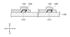
- FIG. 7 is a cross-sectional view showing the difference in shape between two Josephson elements in the first reference example.
- FIG. 8 is a plan view showing a vapor deposition mask used in the second reference example.
- FIG. 9 is a cross-sectional view (part 1) showing a vapor deposition mask used in the second reference example.
- FIG. 10 is a cross-sectional view (part 2) showing a vapor deposition mask used in the second reference example.
- FIG. 11 is a cross-sectional view (part 1) showing a method of manufacturing a Josephson element according to the second reference example.
- FIG. 12 is a cross-sectional view (part 2) showing the method of manufacturing the Josephson element according to the second reference example.
- FIG. 13 is a cross-sectional view showing the difference in shape between two Josephson elements in the second reference example.
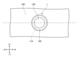
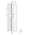
- 14 is a plan view showing the Josephson element according to the first embodiment.
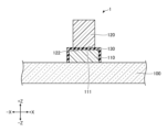
- FIG. 15 is a cross-sectional view showing the Josephson element according to the first embodiment.
- FIG. 16 is a cross-sectional view (part 1) showing the method of manufacturing the Josephson element according to the first embodiment.
- FIG. 17 is a cross-sectional view (part 2) showing the method of manufacturing the Josephson element according to the first embodiment.
- FIG. 18 is a cross-sectional view (No. 3) showing the method of manufacturing the Josephson element according to the first embodiment.
- FIG. 19 is a cross-sectional view (No. 4) showing the method of manufacturing the Josephson element according to the first embodiment.
- FIG. 20 is a cross-sectional view (No. 5) showing the method of manufacturing the Josephson element according to the first embodiment.
- FIG. 21 is a schematic diagram showing the relationship between the substrate and the vapor deposition source during vapor deposition in the first embodiment.
- FIG. 22 is a plan view showing the Josephson element according to the second embodiment.
- FIG. 23 is a cross-sectional view showing a Josephson element according to the second embodiment.
- FIG. 24 is a cross-sectional view (part 1) showing the method of manufacturing the Josephson element according to the second embodiment.
- FIG. 25 is a cross-sectional view (part 2) showing the method of manufacturing the Josephson element according to the second embodiment.
- FIG. 26 is a cross-sectional view (No. 3) showing the method of manufacturing the Josephson element according to the second embodiment.
- FIG. 27 is a cross-sectional view (No. 4) showing the method of manufacturing the Josephson element according to the second embodiment.
- FIG. 28 is a schematic diagram showing the relationship between the substrate and the vapor deposition source during vapor deposition in the second embodiment.
- FIG. 29 is a plan view showing a superconducting circuit according to the third embodiment.
- FIG. 30 is a cross-sectional view showing a superconducting circuit according to the third embodiment.
- FIG. 31 is a cross-sectional view (No. 1) showing the method of manufacturing the superconducting circuit according to the third embodiment.
- FIG. 32 is a cross-sectional view (part 2) showing the method of manufacturing the superconducting circuit according to the third embodiment.
- FIG. 33 is a cross-sectional view (No.
- FIG. 34 is a cross-sectional view (No. 4) showing the method of manufacturing the superconducting circuit according to the third embodiment.
- FIG. 35 is a cross-sectional view (No. 5) showing the method of manufacturing the superconducting circuit according to the third embodiment.
- FIG. 36 is a cross-sectional view (No. 6) showing the method of manufacturing the superconducting circuit according to the third embodiment.
- FIG. 37 is a cross-sectional view (No. 7) showing the method of manufacturing the superconducting circuit according to the third embodiment.
- FIG. 38 is a cross-sectional view (No. 8) showing the method of manufacturing the superconducting circuit according to the third embodiment.
- FIG. 39 is a plan view showing the superconducting circuit according to the fourth embodiment.
- FIG. 40 is a cross-sectional view showing a superconducting circuit according to the fourth embodiment.
- FIG. 41 is a cross-sectional view (part 1) showing the method of manufacturing a superconducting circuit according to the fourth embodiment.
- FIG. 42 is a cross-sectional view (part 2) showing the method of manufacturing the superconducting circuit according to the fourth embodiment.
- FIG. 43 is a cross-sectional view (No. 3) showing the method of manufacturing the superconducting circuit according to the fourth embodiment.
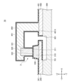
- FIG. 44 is a cross-sectional view showing a superconducting circuit according to the fifth embodiment.
- FIG. 45 is a cross-sectional view (part 1) showing the method of manufacturing the superconducting circuit according to the fifth embodiment.
- FIG. 46 is a cross-sectional view (part 2) showing the method of manufacturing the superconducting circuit according to the fifth embodiment.
- FIG. 47 is a cross-sectional view (No. 3) showing the method of manufacturing the superconducting circuit according to the fifth embodiment.
- FIG. 48 is a cross-sectional view (No. 4) showing the method of manufacturing the superconducting circuit according to the fifth embodiment.
- FIG. 49 is a plan view showing a superconducting circuit according to the sixth embodiment.
- FIG. 50 is a cross-sectional view showing a superconducting circuit according to the sixth embodiment.
- FIG. 51 is a cross-sectional view (No.
- FIG. 52 is a cross-sectional view (part 2) showing the method of manufacturing the superconducting circuit according to the sixth embodiment.
- FIG. 53 is a cross-sectional view (No. 3) showing the method of manufacturing the superconducting circuit according to the sixth embodiment.
- FIG. 54 is a cross-sectional view showing a superconducting circuit according to the seventh embodiment.
- FIG. 55 is a cross-sectional view (No. 1) showing the method of manufacturing the superconducting circuit according to the seventh embodiment.
- FIG. 56 is a cross-sectional view (part 2) showing the method of manufacturing the superconducting circuit according to the seventh embodiment.
- FIG. 57 is a cross-sectional view (No.
- FIG. 58 is a cross-sectional view showing a superconducting circuit according to a modification of the fifth embodiment
- FIG. 59 is a diagram showing a quantum arithmetic device according to the eighth embodiment.
- planar view means planar view from a direction perpendicular to the top surface of the substrate.
- a vapor deposition mask is used to form a superconducting metal layer on a substrate.
- FIG. 1 is a plan view showing a vapor deposition mask used in the first reference example.
- FIG. 2 is a cross-sectional view showing a vapor deposition mask used in the first reference example.
- FIG. 2 corresponds to a cross-sectional view taken along line II-II in FIG. 3 and 4 are cross-sectional views showing the method of manufacturing the Josephson element according to the first reference example.
- 5 and 6 are schematic diagrams showing the relationship between the substrate and the vapor deposition source during vapor deposition in the first reference example.
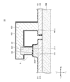
- a vapor deposition mask 1200 used in the first reference example has a first resist layer 1210 and a second resist layer 1220 .
- a first resist layer 1210 is provided on the substrate 1100 and a second resist layer 1220 is provided on the first resist layer 1210 .
- the second resist layer 1220 has a first opening pattern 1221 extending in the X-axis direction parallel to the top surface of the substrate 1100, and a second opening pattern 1222 extending in the Y-axis direction parallel to the top surface of the substrate 1100 and perpendicular to the X-axis direction.
- the second opening pattern 1222 is positioned near one end of the first opening pattern 1221 .
- the first resist layer 1210 has an opening pattern 1211 surrounding at least the first opening pattern 1221 and the second opening pattern 1222 in plan view from the Z-axis direction perpendicular to the upper surface of the substrate 1100 .
- the first superconducting metal layer 1310 is formed on the substrate 1100 by vapor deposition.
- the Z-axis direction of the substrate 1100 is made non-parallel to the traveling direction 1501 of the evaporated material emitted from the evaporation source 1500 .
- the direction inclined from the +Z side to the +X side of the substrate 1100 is defined as a direction parallel to the traveling direction 1501 .
- the inclination angle ⁇ 1 is such that the vapor passes through both the first opening pattern 1221 and the second opening pattern 1222 .
- the first superconducting metal layer 1310 is formed at a position shifted to the -X side from the first opening pattern 1221 and the second opening pattern 1222 in plan view from the Z-axis direction.
- the first superconducting metal layer 1310 has a first pattern 1311 composed of the evaporated raw material passed through the first opening pattern 1221 and a second pattern 1312 composed of the evaporated raw material passed through the second opening pattern 1222 .
- the first pattern 1311 extends in the X-axis direction like the first opening pattern 1221
- the second pattern 1312 extends in the Y-axis direction like the second opening pattern 1222 .
- the surface of the first superconducting metal layer 1310 is oxidized to form an oxide film 1330, as shown in FIG.
- a second superconducting metal layer 1320 is formed on the substrate 1100 and the oxide film 1330 by vapor deposition.
- the Z-axis direction of the substrate 1100 is made non-parallel to the traveling direction 1501 of the evaporated material emitted from the deposition source 1500 .
- the direction inclined from the +Z side to the ⁇ X side of the substrate 1100 is defined as a direction parallel to the traveling direction 1501 .
- the second superconducting metal layer 1320 is formed at a position shifted to the +X side from the first opening pattern 1221 and the second opening pattern 1222 in plan view from the Z-axis direction.
- the second superconducting metal layer 1320 has a first pattern 1321 composed of the evaporated raw material passed through the first opening pattern 1221 and a second pattern 1322 composed of the evaporated raw material passed through the second opening pattern 1222 .
- the first pattern 1321 extends in the X-axis direction like the first opening pattern 1221
- the second pattern 1322 extends in the Y-axis direction like the second opening pattern 1222 .
- a second pattern 1312 of the first superconducting metal layer 1310 and a first pattern 1321 of the second superconducting metal layer 1320 are laminated with an oxide film 1330 interposed therebetween.
- the second pattern 1312 of the first superconducting metal layer 1310, the oxide film 1330, and the first pattern 1321 of the second superconducting metal layer 1320 constitute the Josephson element.
- the incident angle of the evaporated material onto the substrate 1100 differs depending on the position in the X-axis direction.
- the incident angle to the center of the substrate 1100 is 90°- ⁇ 1
- the incident angle to the vicinity of the +X side edge of the substrate 1100 is larger than 90° ⁇ 1
- the incident angle to the +X side edge of the substrate 1100 is smaller than 90° ⁇ 1.
- the diameter of the substrate 1100 is 6 inches (approximately 15 cm)
- the distance between the center of the substrate 1100 and the deposition source 1500 is 60 cm
- the tilt angle ⁇ 1 is 30°
- the incident angle to the center of the substrate 1100 is 60°
- the incident angle to the +X side edge of the substrate 1100 is 66.3°
- the incident angle to the vicinity of the +X side edge of the substrate 1100 is 54.2°. Therefore, there is a maximum difference of 12.1° in the incident angle.
- the angle of incidence of the evaporated material on the substrate 1100 when forming the second superconducting metal layer 1320 also differs depending on the position in the X-axis direction.
- the incident angle to the center of the substrate 1100 is 90°- ⁇ 2
- the incident angle to the +X side edge of the substrate 1100 is smaller than 90° ⁇ 2
- the incident angle to the +X side edge of the substrate 1100 is larger than 90° ⁇ 1.
- FIG. 7 is a cross-sectional view showing the difference in shape between two Josephson elements in the first reference example.
- FIG. 8 is a plan view showing a vapor deposition mask used in the second reference example.
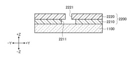
- 9 and 10 are cross-sectional views showing vapor deposition masks used in the second reference example.
- 9 corresponds to a cross-sectional view taken along line IX-IX in FIG. 8
- FIG. 10 corresponds to a cross-sectional view taken along line XX in FIG. 11 and 12 are cross-sectional views showing a method of manufacturing a Josephson element according to the second reference example.
- 11 and 12 correspond to cross-sectional views taken along line XI-XI in FIG.
- a deposition mask 2200 used in the second reference example has a first resist layer 2210 and a second resist layer 2220 .
- a first resist layer 2210 is provided on the substrate 1100 and a second resist layer 2220 is provided on the first resist layer 2210 .
- the second resist layer 2220 has a first opening pattern 2221 extending in the X-axis direction parallel to the top surface of the substrate 1100, and a second opening pattern 2222 extending in the Y-axis direction parallel to the top surface of the substrate 1100 and perpendicular to the X-axis direction.
- the first opening pattern 2221 and the second opening pattern 2222 cross each other near the center in the longitudinal direction.
- the first resist layer 2210 has a first opening pattern 2211 surrounding the first opening pattern 2221 and a second opening pattern 2212 surrounding the second opening pattern 2222 in plan view from the Z-axis direction perpendicular to the upper surface of the substrate 1100.
- the first superconducting metal layer 2310 is formed on the substrate 1100 by vapor deposition.
- the Z-axis direction of the substrate 1100 is made non-parallel to the traveling direction 1501 of the evaporated material emitted from the deposition source.
- the direction inclined from the +Z side to the +X side of the substrate 1100 is defined as a direction parallel to the traveling direction 1501 .
- the inclination angle is such that the vapor passes through the first opening pattern 2221 but cannot pass through the second opening pattern 2222 .
- the first superconducting metal layer 2310 extends in the X-axis direction similarly to the first opening pattern 2221 .
- the surface of the first superconducting metal layer 2310 is oxidized to form an oxide film 2330, as shown in FIG.
- a second superconducting metal layer 2320 is formed on the substrate 1100 and the oxide film 2330 by vapor deposition.
- the Z-axis direction of the substrate 1100 is made non-parallel to the traveling direction 1501 of the evaporated substance emitted from the deposition source 1500 .
- the direction inclined from the +Z side to the +Y side of the substrate 1100 is defined as a direction parallel to the traveling direction 1501 .
- the inclination angle is such that the vapor passes through the second opening pattern 2222 but cannot pass through the first opening pattern 2221 .
- the second superconducting metal layer 2320 extends in the Y-axis direction similarly to the second opening pattern 2222 . That is, the first superconducting metal layer 2310 and the second superconducting metal layer 2320 intersect.
- a first superconducting metal layer 2310 and a second superconducting metal layer 2320 are laminated with an oxide film 2330 interposed therebetween.
- a Josephson element is composed of the first superconducting metal layer 2310 , the oxide film 2330 and the second superconducting metal layer 2320 .
- the incident angle of the evaporated material to the substrate 1100 when forming the first superconducting metal layer 2310 differs according to the position in the X-axis direction
- the incident angle of the evaporated material to the substrate 1100 when forming the second superconducting metal layer 2320 varies depending on the position in the Y-axis direction.
- FIG. 13 is a cross-sectional view showing the difference in shape between two Josephson elements in the second reference example.
- FIG. 14 is a plan view showing the Josephson element according to the first embodiment.
- FIG. FIG. 15 is a cross-sectional view showing the Josephson element according to the first embodiment.
- FIG. 15 corresponds to a cross-sectional view taken along line XV-XV in FIG.
- the Josephson element 1 has a first superconducting metal layer 110, a second superconducting metal layer 120, and an insulating layer .
- the first superconducting metal layer 110 has a top surface 111 and the second superconducting metal layer 120 has a bottom surface 122 .
- Lower surface 122 faces upper surface 111 .
- Both the first superconducting metal layer 110 and the second superconducting metal layer 120 are substantially columnar.
- the insulating layer 130 is provided between the top surface 111 of the first superconducting metal layer 110 and the bottom surface 122 of the second superconducting metal layer 120 .
- the contour of the lower surface 122 is inside the contour of the upper surface 111 in plan view from a direction perpendicular to the upper surface 111 .
- the insulating layer 130 may also be provided on the side surfaces of the first superconducting metal layer 110 .
- the Josephson element 1 is provided on a substrate 100, for example.
- the upper surface 111 is an example of a first surface
- the lower surface 122 is an example of a second surface.
- FIG. 16 to 20 are cross-sectional views showing the method of manufacturing the Josephson element 1 according to the first embodiment.
- FIG. 21 is a schematic diagram showing the relationship between the substrate and the vapor deposition source during vapor deposition in the first embodiment.
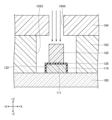
- a resist layer 191 with an opening 191X and a resist layer 192 with an opening 192X are formed on a substrate 100. Then, as shown in FIG. A resist layer 191 is formed on the substrate 100 side of the resist layer 192 .
- the opening 192X has a shape and size corresponding to the upper surface of the first superconducting metal layer 110 to be formed in plan view.
- the opening 191X surrounds the opening 192X in plan view.
- the first superconducting metal layer 110 is formed on the substrate 100 inside the opening 191X by vapor deposition.
- the Z-axis direction of the substrate 100 is made parallel to the traveling direction 151 of the vaporized substance (first vaporized substance) emitted from the vapor deposition source 150 . Therefore, the incident angle of the vaporized material to the center of the substrate 100 is 90°.
- the resist layers 191 and 192 are removed. Although illustration is omitted, the vaporized material is also deposited on the resist layer 192 , but this deposited vaporized material is removed together with the resist layers 191 and 192 . That is, liftoff is performed. Also, the surface (upper surface and side surface) of the first superconducting metal layer 110 is oxidized to form the insulating layer 130 .
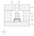
- a resist layer 193 with an opening 193X and a resist layer 194 with an opening 194X are formed on the substrate 100 side of the resist layer 194 .
- the opening 194X surrounds the contour of the top surface 111 of the first superconducting metal layer 110 in plan view and has a shape and size corresponding to the top surface of the second superconducting metal layer 120 to be formed.
- the opening 193X surrounds the opening 194X in plan view.
- the second superconducting metal layer 120 is formed on the portion of the insulating layer 130 above the upper surface 111 of the first superconducting metal layer 110 by vapor deposition inside the opening 193X. Also at this time, as shown in FIG. 21, the Z-axis direction of the substrate 100 is parallel to the traveling direction 151 of the vaporized substance (second vaporized substance). Therefore, the incident angle of the vaporized material to the center of the substrate 100 is 90°.
- the resist layers 193 and 194 are removed (see FIG. 15). Although illustration is omitted, the evaporated material is also deposited on the resist layer 194 , but this deposited evaporated material is removed together with the resist layers 193 and 194 . That is, liftoff is performed.
- the Josephson element 1 according to the first embodiment can be manufactured.
- the contour of the lower surface 122 of the second superconducting metal layer 120 is inside the contour of the upper surface 111 of the first superconducting metal layer 110 in plan view. Therefore, when forming the first superconducting metal layer 110 and when forming the second superconducting metal layer 120, the Z-axis direction of the substrate 100 can be made parallel to the traveling direction 151 of the vaporized material. Therefore, it is possible to suppress the difference in the incident angle of the evaporated material to the substrate 100 .
- the maximum difference in incident angles is 7.1°.
- the difference in shape among the plurality of Josephson elements 1 formed on the substrate 100 is slight, and variations in the characteristics of the Josephson elements 1 can be suppressed.
- FIG. 22 is a plan view showing the Josephson element according to the second embodiment.
- FIG. 23 is a cross-sectional view showing a Josephson element according to the second embodiment.
- FIG. 23 corresponds to a cross-sectional view taken along line XXIII--XXIII in FIG.
- a Josephson element 2 has a first superconducting metal layer 210 , a second superconducting metal layer 220 and an insulating layer 230 .
- the first superconducting metal layer 210 has a top surface 211 and the second superconducting metal layer 220 has a bottom surface 222 . Lower surface 222 faces upper surface 211 .
- the shape of the first superconducting metal layer 110 is substantially truncated cone, and the shape of the second superconducting metal layer 120 is substantially columnar.
- the insulating layer 230 is provided between the top surface 211 of the first superconducting metal layer 210 and the bottom surface 222 of the second superconducting metal layer 220 .
- the contour of the lower surface 222 is inside the contour of the upper surface 211 in plan view from a direction perpendicular to the upper surface 211 .
- the insulating layer 230 may also be provided on the side surfaces of the first superconducting metal layer 210 .
- the Josephson element 2 is provided on a substrate 100, for example.
- the upper surface 211 is an example of a first surface
- the lower surface 222 is an example of a second surface.
- FIG. 24 to 27 are cross-sectional views showing a method of manufacturing the Josephson element 2 according to the second embodiment.
- FIG. 28 is a schematic diagram showing the relationship between the substrate and the vapor deposition source during vapor deposition in the second embodiment.
- a resist layer 291 with an opening 291X and a resist layer 292 with an opening 292X are formed on a substrate 100. Then, as shown in FIG. A resist layer 291 is formed on the substrate 100 side of the resist layer 292 .
- the opening 292X has a shape and size corresponding to the upper surface of the second superconducting metal layer 220 to be formed in plan view.
- the opening 291X has a shape and size surrounding the outline of the lower surface of the first superconducting metal layer 210 to be formed in plan view.
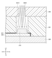
- the first superconducting metal layer 210 is formed on the substrate 100 inside the opening 291X by vapor deposition using the resist layers 291 and 292 as vapor deposition masks.
- the Z-axis direction of the substrate 100 is made non-parallel to the traveling direction 151 of the vaporized substance (first vaporized substance) emitted from the vapor deposition source 150, and the substrate 100 is rotated about a straight line that passes through the center of the upper surface of the substrate 100 and is perpendicular to the upper surface.
- the inclination angle ⁇ 3 is set to such an extent that the lower surface 222 of the second superconducting metal layer 220 to be formed later can be seen from the deposition source 150 at any position in the substrate 100 .
- the inclination angle ⁇ 3 is, for example, about 1° to 10°.
- the surface (top and side surfaces) of the first superconducting metal layer 210 is oxidized to form an insulating layer 230. Then, as shown in FIG. 26, while leaving the resist layers 291 and 292, the surface (top and side surfaces) of the first superconducting metal layer 210 is oxidized to form an insulating layer 230. Then, as shown in FIG. 26, while leaving the resist layers 291 and 292, the surface (top and side surfaces) of the first superconducting metal layer 210 is oxidized to form an insulating layer 230. Then, as shown in FIG.
- the second superconducting metal layer 220 is formed on the portion of the insulating layer 230 above the upper surface 211 of the first superconducting metal layer 210 by vapor deposition inside the opening 291X.
- the Z-axis direction of the substrate 100 is parallel to the advancing direction 151 of the vaporized substance (second vaporized substance). Therefore, the incident angle of the vaporized material to the center of the substrate 100 is 90°.
- the formation of the first superconducting metal layer 210, the formation of the insulating layer 230, and the formation of the second superconducting metal layer 220 are performed continuously in the vacuum chamber while maintaining the vacuum state.
- the resist layers 291 and 292 are removed (see FIG. 23). Although illustration is omitted, the vaporized material also deposits on the resist layer 292 during the formation of the first superconducting metal layer 210 and the formation of the second superconducting metal layer 220, but this deposited vaporized material is removed together with the resist layers 291 and 292. That is, liftoff is performed.
- the Josephson element 1 according to the first embodiment can be manufactured.
- the contour of the lower surface 222 of the second superconducting metal layer 220 is inside the contour of the upper surface 211 of the first superconducting metal layer 210 in plan view. Therefore, the inclination angle ⁇ 1 can be reduced when forming the first superconducting metal layer 210, and the Z-axis direction of the substrate 100 can be parallel to the traveling direction 151 of the vaporized material when forming the second superconducting metal layer 220. Therefore, as in the first embodiment, it is possible to suppress the difference in the angle of incidence of the vaporized material on the substrate 100 .
- the resist layers 191 and 192 can be used to form the first superconducting metal layer 210 and the second superconducting metal layer 220, the throughput can be improved.
- FIG. 29 is a plan view showing a superconducting circuit according to the third embodiment.
- FIG. 30 is a cross-sectional view showing a superconducting circuit according to the third embodiment.
- FIG. 29 shows a perspective view of some components such as an insulating layer.
- FIG. 30 corresponds to a cross-sectional view taken along line XXX-XXX in FIG.
- the superconducting circuit 30 mainly has a substrate 300, a first superconducting metal layer 310, a second superconducting metal layer 320, an insulating layer 330, a third superconducting metal layer 340, a fourth superconducting metal layer 350, and a dielectric layer 390.
- the substrate 300 is, for example, a high resistance Si substrate.
- a third superconducting metal layer 340 is formed on the substrate 300 .
- the third superconducting metal layer 340 extends in the X-axis direction parallel to the top surface of the substrate 300 .
- One end of the third superconducting metal layer 340 has a semi-arcuate shape in plan view.
- the third superconducting metal layer 340 is, for example, an Al layer with a thickness of 30 nm to 70 nm.
- the first superconducting metal layer 310 is formed on the third superconducting metal layer 340 in the vicinity of the semicircular end of the third superconducting metal layer 340 .
- the shape of the first superconducting metal layer 310 is a substantially truncated cone shape.
- the first superconducting metal layer 310 is, for example, an Al layer with a thickness of 30 nm to 70 nm.
- An insulating layer 341 is formed on the surface (upper surface and side surfaces) of the third superconducting metal layer 340 except for the portion where the first superconducting metal layer 310 is formed.
- the insulating layer 341 is, for example, an Al oxide layer with a thickness of 1 nm to 5 nm.
- An insulating layer 330 is formed on the surface (upper surface and side surfaces) of the first superconducting metal layer 310 .
- the insulating layer 330 is, for example, an Al oxide layer with a thickness of 1 nm to 5 nm.
- a second superconducting metal layer 320 is formed on the portion of the insulating layer 330 above the upper surface 311 of the first superconducting metal layer 310 .
- the lower surface 322 of the second superconducting metal layer 320 faces the upper surface 311 of the first superconducting metal layer 310, and a portion of the insulating layer 330 is provided between the upper surface 311 of the first superconducting metal layer 310 and the lower surface 322 of the second superconducting metal layer 320.
- the contour of the lower surface 322 is inside the contour of the upper surface 311 in plan view from a direction perpendicular to the upper surface 311 .
- the shape of the second superconducting metal layer 320 is substantially cylindrical.
- the second superconducting metal layer 320 is, for example, an Al layer with a thickness of 250 nm to 350 nm.
- the upper surface 311 is an example of a first surface
- the lower surface 322 is an example of a second surface.
- a dielectric layer 390 covering the third superconducting metal layer 340 , the insulating layer 341 , the first superconducting metal layer 310 and the insulating layer 330 is formed on the substrate 300 .
- the top surface of the dielectric layer 390 is located above the bottom surface 322 of the second superconducting metal layer 320 and below the top surface of the second superconducting metal layer 320 in the Z-axis direction perpendicular to the top surface of the substrate 300 .
- Dielectric layer 390 is, for example, a benzocyclobutene (BCB) layer.
- An insulating layer 321 is formed on the side surface of the second superconducting metal layer 320 below the upper surface of the dielectric layer 390 . That is, the insulating layer 321 is formed between the second superconducting metal layer 320 and the dielectric layer 390 .
- the insulating layer 321 is, for example, an Al oxide layer with a thickness of 1 nm to 5 nm.
- a fourth superconducting metal layer 350 is formed on the dielectric layer 390 .
- the fourth superconducting metal layer 350 contacts the portion of the second superconducting metal layer 320 above the top surface of the dielectric layer 390 .
- the fourth superconducting metal layer 350 extends in the X-axis direction.
- the fourth superconducting metal layer 350 is, for example, an Al layer with a thickness of 30 nm to 70 nm.
- An insulating layer 351 is formed on the surface (upper surface and side surfaces) of the fourth superconducting metal layer 350 .
- the insulating layer 351 is, for example, an Al oxide layer with a thickness of 1 nm to 5 nm.
- a superconducting circuit 30 includes a Josephson element 3 having a first superconducting metal layer 310 , a second superconducting metal layer 320 and an insulating layer 330 .
- 31 to 38 are cross-sectional views showing the method of manufacturing the superconducting circuit 30 according to the third embodiment.
- the third superconducting metal layer 340 is formed on the substrate 300 .
- the third superconducting metal layer 340 can be formed by vapor deposition and lift-off, for example, similarly to the formation of the first superconducting metal layer 110 in the first embodiment.
- the film formation of the third superconducting metal layer 340 is performed in a vacuum, when the third superconducting metal layer 340 is exposed to the atmosphere, an insulating layer 341 is formed on the surface of the third superconducting metal layer 340 by natural oxidation.
- a resist layer 391 with an opening 391X and a resist layer 392 with an opening 392X are formed on the substrate 300 so as to cover the third superconducting metal layer 340 and the insulating layer 341.
- electron beam exposure can be performed to form a resist layer 391 with an opening 391X and a resist layer 392 with an opening 392X.
- the opening 392X has a shape and size corresponding to the upper surface of the second superconducting metal layer 320 to be formed in plan view.
- the opening 391X has a shape and size surrounding the outline of the lower surface of the first superconducting metal layer 310 to be formed in plan view. Part of the insulating layer 341 is exposed through the openings 391X and 392X.
- the portions of the insulating layer 341 exposed from the openings 391X and 392X are removed by ion milling using Ar ions in vacuum.
- the first superconducting metal layer 310 is formed on the portion of the third superconducting metal layer 340 from which the insulating layer 341 has been removed by vapor deposition using the resist layers 391 and 392 as vapor deposition masks.
- the Z-axis direction of the substrate 300 is made non-parallel to the traveling direction of the vaporized material (first vaporized material) emitted from the vapor deposition source, and the substrate 300 is rotated about a straight line that passes through the center of the upper surface of the substrate 300 and is perpendicular to the upper surface.
- the angle of inclination at this time is such that the lower surface 322 of the second superconducting metal layer 320 to be formed later can be seen from the vapor deposition source at any position in the substrate 300 .
- the inclination angle is, for example, about 1° to 10°.
- the surface (top and side surfaces) of the first superconducting metal layer 310 is oxidized to form an insulating layer 330.
- oxygen is supplied in a vacuum without being exposed to the atmosphere.
- the second superconducting metal layer 320 is formed on the insulating layer 330 above the upper surface 311 of the first superconducting metal layer 310 by vapor deposition using the resist layers 391 and 392 as a vapor deposition mask in a vacuum, inside the opening 391X.
- the Z-axis direction of the substrate 300 is made parallel to the traveling direction of the vaporized substance (second vaporized substance).
- the ion milling of the insulating layer 341, the formation of the first superconducting metal layer 310, the formation of the insulating layer 330, and the formation of the second superconducting metal layer 320 are performed continuously in the vacuum chamber while maintaining the vacuum state.
- the resist layers 391 and 392 are removed.
- the vaporized material also deposits on the resist layer 392 during the formation of the first superconducting metal layer 310 and the formation of the second superconducting metal layer 320, but this deposited vaporized material is removed together with the resist layers 391 and 392. That is, liftoff is performed.
- an insulating layer 321 is formed on the surface of the second superconducting metal layer 320 by natural oxidation.
- a dielectric layer 390 covering the third superconducting metal layer 340, the insulating layer 341, the first superconducting metal layer 310, the insulating layer 330, the second superconducting metal layer 320 and the insulating layer 321 is formed on the substrate 300.
- the top surface of the dielectric layer 390 is located above the top surface of the second superconducting metal layer 320 in the Z-axis direction.
- BCB resin is spin-coated, and then the BCB resin is thermally cured.
- the dielectric layer 390 is etched back by dry etching so that the top surface of the dielectric layer 390 is located below the top surface of the second superconducting metal layer 320 . That is, a portion of the second superconducting metal layer 320 protrudes from the dielectric layer 390 .
- the insulating layer 321 formed on the surface of the portion of the second superconducting metal layer 320 protruding from the dielectric layer 390 is removed, and a fourth superconducting metal layer 350 is formed on the dielectric layer 390 so as to contact the portion of the second superconducting metal layer 320 above the top surface of the dielectric layer 390 (see FIG. 30).
- the insulating layer 321 can be removed by ion milling using Ar ions.
- the fourth superconducting metal layer 350 can be formed, for example, by vapor deposition and lift-off, similar to the formation of the third superconducting metal layer 340, and the like. When the fourth superconducting metal layer 350 is exposed to the atmosphere, an insulating layer 351 is formed on the surface of the fourth superconducting metal layer 350 by natural oxidation.
- the superconducting circuit 30 according to the third embodiment can be manufactured.
- the contour of the lower surface 322 of the second superconducting metal layer 320 is inside the contour of the upper surface 311 of the first superconducting metal layer 310 in plan view. Therefore, the tilt angle when forming the first superconducting metal layer 310 can be reduced, and the Z-axis direction of the substrate 300 can be made parallel to the traveling direction of the vaporized material when forming the second superconducting metal layer 320. Therefore, as in the first embodiment, it is possible to suppress the difference in the angle of incidence of the vaporized material on the substrate 300 .
- the third superconducting metal layer 340 in contact with the first superconducting metal layer 310 and the fourth superconducting metal layer 350 in contact with the second superconducting metal layer 320 can be used as wiring connected to the Josephson element 3.
- FIG. 39 is a plan view showing the superconducting circuit according to the fourth embodiment.
- FIG. 40 is a cross-sectional view showing a superconducting circuit according to the fourth embodiment.
- FIG. 39 shows a perspective view of some components such as an insulating layer.
- FIG. 40 corresponds to a cross-sectional view taken along line XL-XL in FIG.
- the superconducting circuit 40 mainly has a substrate 300, a first superconducting metal layer 310, a second superconducting metal layer 320, an insulating layer 330, a third superconducting metal layer 340, a fourth superconducting metal layer 450, a fifth superconducting metal layer 460, and a dielectric layer 390.
- a fifth superconducting metal layer 460 is formed on the substrate 300 . Like the third superconducting metal layer 340 , the fifth superconducting metal layer 460 extends in the X-axis direction parallel to the upper surface of the substrate 300 . The fifth superconducting metal layer 460 is located on the +X side of the third superconducting metal layer 340 away from the third superconducting metal layer 340 . The fifth superconducting metal layer 460 is, for example, an Al layer with a thickness of 30 nm to 70 nm. An insulating layer 461 is formed on the surface (upper surface and side surfaces) of the fifth superconducting metal layer 460 .
- the insulating layer 461 is, for example, an Al oxide layer with a thickness of 1 nm to 5 nm.
- An opening 461X is formed in the insulating layer 461 so as to overlap with a portion of the fifth superconducting metal layer 460 in plan view.
- the dielectric layer 390 also covers the fifth superconducting metal layer 460 and the insulating layer 461 .
- An opening 490X is formed in the dielectric layer 390 so as to overlap with the opening 461X in plan view.
- a fourth superconducting metal layer 450 is formed on the dielectric layer 390 and inside the openings 490X and 461X.
- the fourth superconducting metal layer 450 contacts the portion of the second superconducting metal layer 320 above the upper surface of the dielectric layer 390 and the fifth superconducting metal layer 460 .
- the fourth superconducting metal layer 450 is, for example, an Al layer.
- the thickness of the portion of the fourth superconducting metal layer 450 above the dielectric layer 390 is, for example, 30 nm to 70 nm.
- An insulating layer 451 is formed on the surface (upper surface and side surfaces) of the fourth superconducting metal layer 450 .
- the insulating layer 451 is, for example, an Al oxide layer with a thickness of 1 nm to 5 nm.
- 41 to 43 are cross-sectional views showing the method of manufacturing the superconducting circuit 40 according to the fourth embodiment.
- the third superconducting metal layer 340 and the fifth superconducting metal layer 460 are formed on the substrate 300 .
- the third superconducting metal layer 340 and the fifth superconducting metal layer 460 can be formed, for example, by vapor deposition and lift-off in the same manner as the formation of the first superconducting metal layer 110 in the first embodiment.
- the film formation of the third superconducting metal layer 340 and the fifth superconducting metal layer 460 is performed in a vacuum, when the third superconducting metal layer 340 and the fifth superconducting metal layer 460 are exposed to the air, the insulating layer 341 is formed on the surface of the third superconducting metal layer 340 and the insulating layer 461 is formed on the surface of the fifth superconducting metal layer 460 by natural oxidation.
- a resist layer 491 having openings 491X is formed on the dielectric layer 390 .
- the opening 491X has a shape and size corresponding to the opening 490X to be formed in plan view.
- the resist layer 491 and the dielectric layer 390 are etched back by dry etching to position the upper surface of the dielectric layer 390 below the upper surface of the second superconducting metal layer 320, thereby forming an opening 490X in the dielectric layer 390.
- the resist layer 491 is removed by etchback.
- the insulating layer 321 formed on the surface of the portion of the second superconducting metal layer 320 protruding from the dielectric layer 390 and the insulating layer 461 exposed from the opening 490X are removed.
- An opening 461X is formed in the insulating layer 461 .
- a fourth superconducting metal layer 450 is formed in contact with the portion of the second superconducting metal layer 320 above the upper surface of the dielectric layer 390 and the fifth superconducting metal layer 460 (see FIG. 40).
- the insulating layers 321 and 461 can be removed by ion milling using Ar ions.
- the fourth superconducting metal layer 450 can be formed, for example, by vapor deposition and lift-off, similar to the formation of the third superconducting metal layer 340 and the fifth superconducting metal layer 460, and the like.
- an insulating layer 451 is formed on the surface of the fourth superconducting metal layer 450 by natural oxidation.
- the superconducting circuit 40 according to the fourth embodiment can be manufactured.
- the third superconducting metal layer 340 in contact with the first superconducting metal layer 310, the fourth superconducting metal layer 450 in contact with the second superconducting metal layer 320, and the fifth superconducting metal layer 460 in contact with the fourth superconducting metal layer 450 can be used as wires connected to the Josephson device 3.
- FIG. 44 is a cross-sectional view showing a superconducting circuit according to the fifth embodiment.
- FIG. 44 like FIG. 40, corresponds to a cross-sectional view taken along line XL-XL in FIG.
- the superconducting circuit 50 mainly has a substrate 300, a first superconducting metal layer 310, a second superconducting metal layer 320, an insulating layer 330, a third superconducting metal layer 340, a fourth superconducting metal layer 450, and a fifth superconducting metal layer 460.
- Superconducting circuit 50 is not provided with dielectric layer 390 .
- the insulating layer 451 is formed on substantially the entire side surface of the fourth superconducting metal layer 450 so as to be connected to the insulating layer 461 .
- 45 to 48 are cross-sectional views showing the method of manufacturing the superconducting circuit 50 according to the fifth embodiment.
- the resist layers 391 and 392 are removed in the same manner as in the fourth embodiment.
- a sacrificial layer 590 covering the third superconducting metal layer 340 , the insulating layer 341 , the first superconducting metal layer 310 , the insulating layer 330 , the second superconducting metal layer 320 and the insulating layer 321 is then formed on the substrate 300 .
- the top surface of the sacrificial layer 590 is located above the top surface of the second superconducting metal layer 320 in the Z-axis direction.
- polymethylglutarimide (PMGI) resin is spin-coated, and then the PMGI resin is thermally cured.
- a resist layer 591 having openings 591X is formed on the sacrificial layer 590. Then, as shown in FIG. The opening 591X has a shape and size corresponding to a portion extending in the Z-axis direction of the fourth superconducting metal layer 450 to be formed later in plan view.
- the resist layer 591 and the sacrificial layer 590 are etched back by dry etching to form an opening 590X in the sacrificial layer 590 while positioning the upper surface of the sacrificial layer 590 below the upper surface of the second superconducting metal layer 320.
- the resist layer 591 is removed by etching back.
- the insulating layer 321 formed on the surface of the portion of the second superconducting metal layer 320 protruding from the sacrificial layer 590 and the insulating layer 461 exposed from the opening 590X are removed in a vacuum.
- An opening 461X is formed in the insulating layer 461 .
- the fourth superconducting metal layer 450 is formed in contact with the portion of the second superconducting metal layer 320 above the upper surface of the sacrificial layer 590 and the fifth superconducting metal layer 460 .
- an insulating layer 451 is formed on the surface of the fourth superconducting metal layer 450 by natural oxidation.
- the sacrificial layer 590 is dissolved using a solvent and removed (see FIG. 44).
- the superconducting circuit 50 according to the fifth embodiment can be manufactured.
- dielectrics contain a defect called a two-level system (TLS), so if the dielectric exists near the Josephson element, it is difficult to extend the coherence time.
- TLS two-level system
- the superconducting circuit 50 has an air bridge structure, and the dielectric layer 390 is not provided around the Josephson element 3 . Therefore, according to this embodiment, the coherence time of the Josephson element 3 can be extended, which is suitable for quantum computation.
- FIG. 49 is a plan view showing a superconducting circuit according to the sixth embodiment.
- FIG. 50 is a cross-sectional view showing a superconducting circuit according to the sixth embodiment.
- FIG. 50 corresponds to a cross-sectional view taken along line LL in FIG.
- trenches 601 are formed in the surface of the substrate 300 along the edges of the third superconducting metal layer 340 and the insulating layer 341 around the Josephson element 3 .
- the trench 601 is formed along the edge of the semi-arcuate end of the third superconducting metal layer 340 in a plan view and the edge of the insulating layer 341 formed on the side thereof.
- the depth of trench 601 is, for example, 50 nm to 200 nm.
- 51 to 53 are cross-sectional views showing the method of manufacturing the superconducting circuit 60 according to the sixth embodiment.
- a third superconducting metal layer 340 and a fifth superconducting metal layer 460 are formed on a substrate 300 in the same manner as in the fourth embodiment.
- natural oxidation forms an insulating layer 341 on the surface of the third superconducting metal layer 340 and an insulating layer 461 on the surface of the fifth superconducting metal layer 460.
- a resist layer 691 having an opening 691X is formed on the substrate 300 so as to cover the third superconducting metal layer 340, the insulating layer 341, the fifth superconducting metal layer 460 and the insulating layer 461.
- the opening 691X has a shape and size corresponding to the trench 601 to be formed in plan view.
- trenches 601 are formed in the surface of the substrate 300 by dry etching using the resist layer 691 as an etching mask.
- the resist layer 691 is removed, and similarly to the fifth embodiment, a resist layer 391 with an opening 391X and a resist layer 392 with an opening 392X are formed on the substrate 300. At this time, the resist layer 391 is also formed inside the trench 601 .
- processing from removal of the insulating layer 341 to removal of the sacrificial layer 590 is performed (see FIG. 50).
- the superconducting circuit 60 according to the sixth embodiment can be manufactured.
- the trench 601 is formed on the surface of the substrate 300, the distance of the Josephson element 3 from the TLS present on the surface of the substrate 300 can be increased, and the dielectric loss can be reduced. Therefore, the coherence time of the Josephson element 3 can be further extended.
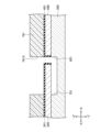
- FIG. 54 is a cross-sectional view showing a superconducting circuit according to the seventh embodiment.
- FIG. 54 like FIG. 50, corresponds to a cross-sectional view taken along line LL in FIG.
- trenches 601 are formed in the surface of the substrate 300 along the edges of the third superconducting metal layer 340 and the insulating layer 341 around the Josephson element 3. Further, a recess 701 connected to the trench 601 is formed in the surface of the substrate 300 below the Josephson element 3 . Therefore, a space exists between the third superconducting metal layer 340 and the substrate 300 .
- An insulating layer 341 is also formed on the lower surface (surface on the ⁇ Z side) of the third superconducting metal layer 340 .
- the depth of trench 601 and recess 701 is, for example, 50 nm to 200 nm.
- 55 to 57 are cross-sectional views showing the method of manufacturing the superconducting circuit 70 according to the seventh embodiment.
- a third superconducting metal layer 340 and a fifth superconducting metal layer 460 are formed on a substrate 300 in the same manner as in the fourth embodiment.
- natural oxidation forms an insulating layer 341 on the surface of the third superconducting metal layer 340 and an insulating layer 461 on the surface of the fifth superconducting metal layer 460.
- a resist layer 791 having openings 791X is formed on the substrate 300 so as to cover the third superconducting metal layer 340, the insulating layer 341, the fifth superconducting metal layer 460 and the insulating layer 461.
- the opening 791X has a shape and size corresponding to the trench 601 and the recess 701 to be formed in plan view.
- trenches 601 and recesses 701 are formed on the surface of the substrate 300 by dry etching using the resist layer 791 as an etching mask.
- side etching of the substrate 300 can be easily caused by setting the dry etching pressure higher than that in forming the trenches 601 in the sixth embodiment.
- the resist layer 791 is removed, and similarly to the fifth embodiment, a resist layer 391 with an opening 391X and a resist layer 392 with an opening 392X are formed on the substrate 300. At this time, the resist layer 391 is also formed inside the trench 601 and the recess 701 . Further, when the third superconducting metal layer 340 is exposed to the atmosphere after the formation of the recess 701, the insulating layer 341 is also formed on the lower surface of the third superconducting metal layer 340 due to natural oxidation.
- the superconducting circuit 70 according to the seventh embodiment can be manufactured.
- the dielectric loss can be further reduced. Therefore, the coherence time of the Josephson element 3 can be further extended.
- the material of the superconducting metal layer is not particularly limited.
- the material of the superconducting metal layer may be Al, Nb, Nb nitride, Ta, Ta nitride, Ti nitride, or the like. That is, the superconducting metal layer may contain Al, Nb, Nb nitride, Ta, Ta nitride, Ti nitride, and the like.
- the third superconducting metal layer 340 and the fifth superconducting metal layer 460 may be Nb layers.
- each superconducting metal layer may have a laminated structure.
- FIG. 58 is a cross-sectional view showing a superconducting circuit according to a modification of the fifth embodiment;
- the first superconducting metal layer 310 has a sixth superconducting metal layer 310A in contact with the third superconducting metal layer 340, and a seventh superconducting metal layer 310B on the sixth superconducting metal layer 310A.
- the sixth superconducting metal layer 310A is an Al layer and the seventh superconducting metal layer 310B is an Nb layer.
- the third superconducting metal layer 340 and the fifth superconducting metal layer 460 may be Ti nitride layers
- the fourth superconducting metal layer 350 may be a Ta layer.
- FIG. 59 is a diagram showing a quantum arithmetic device according to the eighth embodiment.
- a quantum arithmetic device 800 has a qubit chip 810, a signal generator 820, a signal demodulator 830, and a cryogenic dilution refrigerator 840, as shown in FIG.
- the qubit chip 810 is housed in a cryogenic dilution refrigerator 840 and cooled to a temperature below 10 mK.
- a signal generator 820 generates a microwave pulse signal, and the microwave pulse signal is input to the qubit chip 810 .
- a qubit chip 810 outputs a signal corresponding to the microwave pulse signal, and a signal demodulator 830 demodulates the signal output from the qubit chip 810 .
- the signal generator 820 and the signal demodulator 830 are used at room temperature, for example.
- a qubit chip 810 includes a plurality of superconducting qubits 850 , each superconducting qubit 850 having a Josephson element 851 and a capacitor 852 electrically connected in parallel to the Josephson element 851 .
- the Josephson element 851 is the Josephson element 3 in any one of the third to seventh embodiments, and the wiring of the third superconducting metal layer and the wiring of the fourth superconducting metal layer or the fifth superconducting metal layer are connected to the capacitor 852.
- the Josephson element 851 included in the quantum arithmetic device 800 according to the eighth embodiment is the Josephson element 3 according to any one of the third to seventh embodiments, variations in characteristics among the plurality of Josephson elements 3 are suppressed, and excellent reliability calculations can be performed.
Landscapes
- Engineering & Computer Science (AREA)
- General Physics & Mathematics (AREA)
- Theoretical Computer Science (AREA)
- Physics & Mathematics (AREA)
- Manufacturing & Machinery (AREA)
- Mathematical Analysis (AREA)
- Evolutionary Computation (AREA)
- Data Mining & Analysis (AREA)
- Condensed Matter Physics & Semiconductors (AREA)
- Mathematical Optimization (AREA)
- Pure & Applied Mathematics (AREA)
- Computing Systems (AREA)
- General Engineering & Computer Science (AREA)
- Mathematical Physics (AREA)
- Software Systems (AREA)
- Computational Mathematics (AREA)
- Artificial Intelligence (AREA)
- Superconductor Devices And Manufacturing Methods Thereof (AREA)
Priority Applications (4)
| Application Number | Priority Date | Filing Date | Title |
|---|---|---|---|
| JP2023575022A JP7806814B2 (ja) | 2022-01-24 | 2022-01-24 | ジョセフソン素子、超伝導回路、量子演算装置及びジョセフソン素子の製造方法 |
| PCT/JP2022/002371 WO2023139779A1 (ja) | 2022-01-24 | 2022-01-24 | ジョセフソン素子、超伝導回路、量子演算装置及びジョセフソン素子の製造方法 |
| EP22921936.5A EP4471830B1 (en) | 2022-01-24 | 2022-01-24 | Superconducting circuit including a josephson element, quantum computation device, and method for manufacturing the josephson element |
| US18/743,239 US20240431216A1 (en) | 2022-01-24 | 2024-06-14 | Josephson device, superconducting circuit, quantum operation device, and method for manufacturing josephson device |
Applications Claiming Priority (1)
| Application Number | Priority Date | Filing Date | Title |
|---|---|---|---|
| PCT/JP2022/002371 WO2023139779A1 (ja) | 2022-01-24 | 2022-01-24 | ジョセフソン素子、超伝導回路、量子演算装置及びジョセフソン素子の製造方法 |
Related Child Applications (1)
| Application Number | Title | Priority Date | Filing Date |
|---|---|---|---|
| US18/743,239 Continuation US20240431216A1 (en) | 2022-01-24 | 2024-06-14 | Josephson device, superconducting circuit, quantum operation device, and method for manufacturing josephson device |
Publications (1)
| Publication Number | Publication Date |
|---|---|
| WO2023139779A1 true WO2023139779A1 (ja) | 2023-07-27 |
Family
ID=87348417
Family Applications (1)
| Application Number | Title | Priority Date | Filing Date |
|---|---|---|---|
| PCT/JP2022/002371 Ceased WO2023139779A1 (ja) | 2022-01-24 | 2022-01-24 | ジョセフソン素子、超伝導回路、量子演算装置及びジョセフソン素子の製造方法 |
Country Status (4)
| Country | Link |
|---|---|
| US (1) | US20240431216A1 (https=) |
| EP (1) | EP4471830B1 (https=) |
| JP (1) | JP7806814B2 (https=) |
| WO (1) | WO2023139779A1 (https=) |
Cited By (2)
| Publication number | Priority date | Publication date | Assignee | Title |
|---|---|---|---|---|
| JP2024516062A (ja) * | 2022-03-29 | 2024-04-12 | ▲騰▼▲訊▼科技(深▲セン▼)有限公司 | ジョセフソン接合の製造方法、及び生産ライン設備 |
| EP4626212A1 (en) * | 2024-03-26 | 2025-10-01 | Fujitsu Limited | Method for manufacturing a josephson device, josephson device, and qubit including the same |
Citations (10)
| Publication number | Priority date | Publication date | Assignee | Title |
|---|---|---|---|---|
| JPH02288403A (ja) | 1989-04-27 | 1990-11-28 | Nec Corp | 超伝導モノリシック集積回路およびその製造方法 |
| JPH03190289A (ja) * | 1989-12-20 | 1991-08-20 | Fujitsu Ltd | ジョセフソン接合素子及びその製造方法 |
| JPH04346277A (ja) * | 1991-05-24 | 1992-12-02 | Nec Corp | 層状超伝導体回路とその製造方法 |
| JPH05102547A (ja) * | 1991-05-30 | 1993-04-23 | Fujitsu Ltd | ジヨセフソン集積回路装置の製造方法 |
| JPH05243628A (ja) * | 1992-02-28 | 1993-09-21 | Fujitsu Ltd | ジョセフソン接合素子及びその製造方法 |
| JPH05315659A (ja) | 1992-05-06 | 1993-11-26 | Nippon Steel Corp | 放射線検出素子 |
| US20040183065A1 (en) | 2003-02-12 | 2004-09-23 | Kerber George L. | Self-aligned junction passivation for superconductor integrated circuit |
| US20150340584A1 (en) | 2013-03-15 | 2015-11-26 | International Business Machines Corporation | Suspended superconducting qubits |
| US20160093790A1 (en) * | 2014-09-26 | 2016-03-31 | International Business Machines Corporation | Diamond substrates for superconducting quantum circuits |
| JP2020535461A (ja) * | 2017-09-18 | 2020-12-03 | グーグル エルエルシー | 2段階成膜プロセスにおける接合抵抗の変動の低減 |
Family Cites Families (4)
| Publication number | Priority date | Publication date | Assignee | Title |
|---|---|---|---|---|
| US7615385B2 (en) * | 2006-09-20 | 2009-11-10 | Hypres, Inc | Double-masking technique for increasing fabrication yield in superconducting electronics |
| WO2019117883A1 (en) * | 2017-12-13 | 2019-06-20 | Intel Corporation | Qubit devices with josephson junctions fabricated using air bridge or cantilever |
| US10256392B1 (en) * | 2018-03-23 | 2019-04-09 | International Business Machines Corporation | Vertical transmon qubit device |
| CN113921691B (zh) * | 2021-12-07 | 2022-03-18 | 材料科学姑苏实验室 | 一种约瑟夫森结、约瑟夫森结阵列、其制备方法和用途 |
-
2022
- 2022-01-24 EP EP22921936.5A patent/EP4471830B1/en active Active
- 2022-01-24 WO PCT/JP2022/002371 patent/WO2023139779A1/ja not_active Ceased
- 2022-01-24 JP JP2023575022A patent/JP7806814B2/ja active Active
-
2024
- 2024-06-14 US US18/743,239 patent/US20240431216A1/en active Pending
Patent Citations (10)
| Publication number | Priority date | Publication date | Assignee | Title |
|---|---|---|---|---|
| JPH02288403A (ja) | 1989-04-27 | 1990-11-28 | Nec Corp | 超伝導モノリシック集積回路およびその製造方法 |
| JPH03190289A (ja) * | 1989-12-20 | 1991-08-20 | Fujitsu Ltd | ジョセフソン接合素子及びその製造方法 |
| JPH04346277A (ja) * | 1991-05-24 | 1992-12-02 | Nec Corp | 層状超伝導体回路とその製造方法 |
| JPH05102547A (ja) * | 1991-05-30 | 1993-04-23 | Fujitsu Ltd | ジヨセフソン集積回路装置の製造方法 |
| JPH05243628A (ja) * | 1992-02-28 | 1993-09-21 | Fujitsu Ltd | ジョセフソン接合素子及びその製造方法 |
| JPH05315659A (ja) | 1992-05-06 | 1993-11-26 | Nippon Steel Corp | 放射線検出素子 |
| US20040183065A1 (en) | 2003-02-12 | 2004-09-23 | Kerber George L. | Self-aligned junction passivation for superconductor integrated circuit |
| US20150340584A1 (en) | 2013-03-15 | 2015-11-26 | International Business Machines Corporation | Suspended superconducting qubits |
| US20160093790A1 (en) * | 2014-09-26 | 2016-03-31 | International Business Machines Corporation | Diamond substrates for superconducting quantum circuits |
| JP2020535461A (ja) * | 2017-09-18 | 2020-12-03 | グーグル エルエルシー | 2段階成膜プロセスにおける接合抵抗の変動の低減 |
Non-Patent Citations (1)
| Title |
|---|
| See also references of EP4471830A4 |
Cited By (4)
| Publication number | Priority date | Publication date | Assignee | Title |
|---|---|---|---|---|
| JP2024516062A (ja) * | 2022-03-29 | 2024-04-12 | ▲騰▼▲訊▼科技(深▲セン▼)有限公司 | ジョセフソン接合の製造方法、及び生産ライン設備 |
| JP7747765B2 (ja) | 2022-03-29 | 2025-10-01 | ▲騰▼▲訊▼科技(深▲セン▼)有限公司 | ジョセフソン接合の製造方法、及び生産ライン設備 |
| US12550626B2 (en) | 2022-03-29 | 2026-02-10 | Tencent Technology (Shenzhen) Company Limited | Method for preparing josephson junction and production line device |
| EP4626212A1 (en) * | 2024-03-26 | 2025-10-01 | Fujitsu Limited | Method for manufacturing a josephson device, josephson device, and qubit including the same |
Also Published As
| Publication number | Publication date |
|---|---|
| JPWO2023139779A1 (https=) | 2023-07-27 |
| US20240431216A1 (en) | 2024-12-26 |
| JP7806814B2 (ja) | 2026-01-27 |
| EP4471830A1 (en) | 2024-12-04 |
| EP4471830B1 (en) | 2025-12-10 |
| EP4471830A4 (en) | 2025-03-12 |
Similar Documents
| Publication | Publication Date | Title |
|---|---|---|
| US20240431216A1 (en) | Josephson device, superconducting circuit, quantum operation device, and method for manufacturing josephson device | |
| KR100780986B1 (ko) | 반도체장치 및 그 제조방법 | |
| JPS60138940A (ja) | 半導体装置の製造方法 | |
| TWI859495B (zh) | 超導裝置和用於製造超導裝置之方法 | |
| JP7567933B2 (ja) | 量子デバイス及びその製造方法 | |
| JPWO2023139779A5 (https=) | ||
| JP7567934B2 (ja) | 量子デバイス及びその製造方法 | |
| JP4081751B2 (ja) | 配線構造の製造方法 | |
| WO2024069696A1 (ja) | 量子デバイス、量子演算装置及び量子デバイスの製造方法 | |
| US20240321779A1 (en) | Interconnection member and method of manufacturing the same | |
| WO2023132064A1 (ja) | 量子演算装置及び量子演算装置の製造方法 | |
| US20260047349A1 (en) | Superconducting quantum circuit, quantum device, and method for manufacturing superconducting quantum circuit | |
| JP2006294771A (ja) | 半導体装置の製造方法 | |
| US8129791B2 (en) | Semiconductor device having a contact plug and manufacturing method thereof | |
| EP4694659A1 (en) | Method of manufacturing quantum device and quantum device | |
| JPH01208842A (ja) | 半導体集積回路装置の製造方法 | |
| US20250228141A1 (en) | Method for manufacturing josephson junction device and method for manufacturing quantum bit device | |
| WO2024232051A1 (ja) | デバイスおよびデバイスの製造方法 | |
| WO2023199419A1 (ja) | ジョセフソン接合素子、量子デバイス及びジョセフソン接合素子の製造方法 | |
| WO2023243080A1 (ja) | ジョセフソン接合素子の製造方法および量子ビットの製造方法 | |
| JP2025164639A (ja) | 水晶発振器 | |
| KR20240117866A (ko) | 조셉슨 접합 소자, 조셉슨 접합 소자를 포함하는 초전도 큐비트, 및 조셉슨 접합 소자의 제조 방법 | |
| HK40089873A (zh) | 硅通孔互连结构及其制备方法 | |
| JPH03205829A (ja) | 半導体装置の製造方法 | |
| CN115206932A (zh) | 叠层结构、叠层结构制作方法及显示面板 |
Legal Events
| Date | Code | Title | Description |
|---|---|---|---|
| ENP | Entry into the national phase |
Ref document number: 2023575022 Country of ref document: JP Kind code of ref document: A |
|
| NENP | Non-entry into the national phase |
Ref country code: DE |
|
| ENP | Entry into the national phase |
Ref document number: 2022921936 Country of ref document: EP Effective date: 20240826 |
|
| WWG | Wipo information: grant in national office |
Ref document number: 2022921936 Country of ref document: EP |