WO2023127725A1 - スティフナ付き配線基板 - Google Patents
スティフナ付き配線基板 Download PDFInfo
- Publication number
- WO2023127725A1 WO2023127725A1 PCT/JP2022/047631 JP2022047631W WO2023127725A1 WO 2023127725 A1 WO2023127725 A1 WO 2023127725A1 JP 2022047631 W JP2022047631 W JP 2022047631W WO 2023127725 A1 WO2023127725 A1 WO 2023127725A1
- Authority
- WO
- WIPO (PCT)
- Prior art keywords
- stiffener
- wiring board
- thermal expansion
- coefficient
- layer
- Prior art date
- Legal status (The legal status is an assumption and is not a legal conclusion. Google has not performed a legal analysis and makes no representation as to the accuracy of the status listed.)
- Ceased
Links
Images





Classifications
-
- H—ELECTRICITY
- H05—ELECTRIC TECHNIQUES NOT OTHERWISE PROVIDED FOR
- H05K—PRINTED CIRCUITS; CASINGS OR CONSTRUCTIONAL DETAILS OF ELECTRIC APPARATUS; MANUFACTURE OF ASSEMBLAGES OF ELECTRICAL COMPONENTS
- H05K1/00—Printed circuits
- H05K1/18—Printed circuits structurally associated with non-printed electric components
- H05K1/181—Printed circuits structurally associated with non-printed electric components associated with surface mounted components
-
- H—ELECTRICITY
- H05—ELECTRIC TECHNIQUES NOT OTHERWISE PROVIDED FOR
- H05K—PRINTED CIRCUITS; CASINGS OR CONSTRUCTIONAL DETAILS OF ELECTRIC APPARATUS; MANUFACTURE OF ASSEMBLAGES OF ELECTRICAL COMPONENTS
- H05K1/00—Printed circuits
- H05K1/02—Details
-
- H—ELECTRICITY
- H05—ELECTRIC TECHNIQUES NOT OTHERWISE PROVIDED FOR
- H05K—PRINTED CIRCUITS; CASINGS OR CONSTRUCTIONAL DETAILS OF ELECTRIC APPARATUS; MANUFACTURE OF ASSEMBLAGES OF ELECTRICAL COMPONENTS
- H05K1/00—Printed circuits
- H05K1/02—Details
- H05K1/0271—Arrangements for reducing stress or warp in rigid printed circuit boards, e.g. caused by loads, vibrations or differences in thermal expansion
-
- H—ELECTRICITY
- H05—ELECTRIC TECHNIQUES NOT OTHERWISE PROVIDED FOR
- H05K—PRINTED CIRCUITS; CASINGS OR CONSTRUCTIONAL DETAILS OF ELECTRIC APPARATUS; MANUFACTURE OF ASSEMBLAGES OF ELECTRICAL COMPONENTS
- H05K3/00—Apparatus or processes for manufacturing printed circuits
- H05K3/0058—Laminating printed circuit boards onto other substrates, e.g. metallic substrates
-
- H—ELECTRICITY
- H10—SEMICONDUCTOR DEVICES; ELECTRIC SOLID-STATE DEVICES NOT OTHERWISE PROVIDED FOR
- H10W—GENERIC PACKAGES, INTERCONNECTIONS, CONNECTORS OR OTHER CONSTRUCTIONAL DETAILS OF DEVICES COVERED BY CLASS H10
- H10W70/00—Package substrates; Interposers; Redistribution layers [RDL]
- H10W70/60—Insulating or insulated package substrates; Interposers; Redistribution layers
-
- H—ELECTRICITY
- H10—SEMICONDUCTOR DEVICES; ELECTRIC SOLID-STATE DEVICES NOT OTHERWISE PROVIDED FOR
- H10W—GENERIC PACKAGES, INTERCONNECTIONS, CONNECTORS OR OTHER CONSTRUCTIONAL DETAILS OF DEVICES COVERED BY CLASS H10
- H10W70/00—Package substrates; Interposers; Redistribution layers [RDL]
- H10W70/60—Insulating or insulated package substrates; Interposers; Redistribution layers
- H10W70/67—Insulating or insulated package substrates; Interposers; Redistribution layers characterised by their insulating layers or insulating parts
- H10W70/69—Insulating materials thereof
- H10W70/698—Semiconductor materials that are electrically insulating, e.g. undoped silicon
-
- H—ELECTRICITY
- H05—ELECTRIC TECHNIQUES NOT OTHERWISE PROVIDED FOR
- H05K—PRINTED CIRCUITS; CASINGS OR CONSTRUCTIONAL DETAILS OF ELECTRIC APPARATUS; MANUFACTURE OF ASSEMBLAGES OF ELECTRICAL COMPONENTS
- H05K2201/00—Indexing scheme relating to printed circuits covered by H05K1/00
- H05K2201/06—Thermal details
- H05K2201/068—Thermal details wherein the coefficient of thermal expansion is important
-
- H—ELECTRICITY
- H05—ELECTRIC TECHNIQUES NOT OTHERWISE PROVIDED FOR
- H05K—PRINTED CIRCUITS; CASINGS OR CONSTRUCTIONAL DETAILS OF ELECTRIC APPARATUS; MANUFACTURE OF ASSEMBLAGES OF ELECTRICAL COMPONENTS
- H05K2201/00—Indexing scheme relating to printed circuits covered by H05K1/00
- H05K2201/10—Details of components or other objects attached to or integrated in a printed circuit board
- H05K2201/10431—Details of mounted components
- H05K2201/10439—Position of a single component
- H05K2201/10462—Flat component oriented parallel to the PCB surface
-
- H—ELECTRICITY
- H05—ELECTRIC TECHNIQUES NOT OTHERWISE PROVIDED FOR
- H05K—PRINTED CIRCUITS; CASINGS OR CONSTRUCTIONAL DETAILS OF ELECTRIC APPARATUS; MANUFACTURE OF ASSEMBLAGES OF ELECTRICAL COMPONENTS
- H05K2201/00—Indexing scheme relating to printed circuits covered by H05K1/00
- H05K2201/10—Details of components or other objects attached to or integrated in a printed circuit board
- H05K2201/10613—Details of electrical connections of non-printed components, e.g. special leads
- H05K2201/10621—Components characterised by their electrical contacts
- H05K2201/10734—Ball grid array [BGA]; Bump grid array
-
- H—ELECTRICITY
- H10—SEMICONDUCTOR DEVICES; ELECTRIC SOLID-STATE DEVICES NOT OTHERWISE PROVIDED FOR
- H10W—GENERIC PACKAGES, INTERCONNECTIONS, CONNECTORS OR OTHER CONSTRUCTIONAL DETAILS OF DEVICES COVERED BY CLASS H10
- H10W90/00—Package configurations
- H10W90/701—Package configurations characterised by the relative positions of pads or connectors relative to package parts
- H10W90/721—Package configurations characterised by the relative positions of pads or connectors relative to package parts of bump connectors
- H10W90/724—Package configurations characterised by the relative positions of pads or connectors relative to package parts of bump connectors between a chip and a stacked insulating package substrate, interposer or RDL
Definitions
- the present invention relates to a wiring board with a stiffener.
- FC-BGA Flexible Chip Ball Grid Array
- LSI package in which LSI electronic components are mounted on a wiring board.
- Wiring substrates used in such LSI packages are provided with stiffeners for the purpose of reinforcement and warpage correction, as described in Patent Document 1, for example.
- a wiring board with stiffeners includes a wiring board, a mounting area located on the top surface of the wiring board, a first surface located on the top surface of the wiring board and facing the wiring board so as to surround the mounting area, and a first surface facing the wiring board. a stiffener having a second surface opposite the first surface.
- the wiring board has a first coefficient of thermal expansion.
- the stiffener has a first area facing the wiring board and including a first surface and having a second thermal expansion coefficient, and a stiffener located on the surface side opposite to the first area and including a second surface and having a third thermal expansion coefficient. Contains 2 regions. The absolute value of the difference between the first coefficient of thermal expansion and the second coefficient of thermal expansion is smaller than the absolute value of the difference between the first coefficient of thermal expansion and the third coefficient of thermal expansion.
- An electronic component mounting structure includes the wiring board with a stiffener and an electronic component located in the mounting area.
- FIG. 4 is an explanatory diagram for explaining a state in which an electronic component is mounted on the wiring board with a stiffener according to the embodiment of the present disclosure
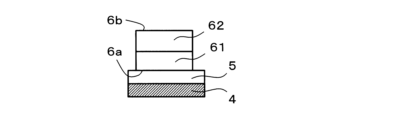
- FIG. 2 is an enlarged explanatory view for explaining a region X shown in FIG. 1
- 4 is a graph showing the results of corner stress simulation and warpage simulation for a stiffener-equipped wiring board provided with copper stiffeners (conventional stiffeners).
- 5 is a graph showing the results of corner stress simulation and warpage simulation for a wiring board with a stiffener assuming that the stiffener has a coefficient of thermal expansion of 20 ppm/° C.
- FIG. 4 is an explanatory diagram for explaining a state in which an electronic component is mounted on the wiring board with a stiffener according to the embodiment of the present disclosure
- FIG. 2 is an enlarged explanatory view for explaining a region X shown in FIG. 1
- 4 is a graph showing the results of corner stress simulation and warpage simulation for a stiffener-equipped wiring board provided with
- FIG. 5 is a graph showing the results of corner stress simulation and warp simulation for a wiring board with a stiffener, assuming that the stiffener has a coefficient of thermal expansion of 15 ppm/° C.
- FIG. 10 is a graph showing the results of corner stress simulation and warpage simulation for a stiffener-equipped wiring board provided with an AlSiC (SiC 40%) stiffener (conventional stiffener).
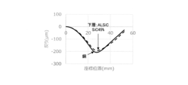
- FIG. 10 is a graph showing the results of corner stress simulation and warpage simulation for a stiffener-equipped wiring board provided with an AlSiC (SiC 45%) stiffener (conventional stiffener).
- FIG. 10 is a graph showing corner stress simulation results and warpage simulation results for a stiffener-equipped wiring board having a stiffener with a lower layer of copper and an upper layer of AlSiC (SiC 40%) (a stiffener outside the scope of the present disclosure).
- FIG. 10 is a graph showing corner stress simulation results and warpage simulation results for a stiffener-equipped wiring board having stiffeners with a lower layer of copper and an upper layer of AlSiC (SiC 45%) (stiffeners outside the scope of the present disclosure).
- 4 is a graph showing corner stress simulation results and warpage simulation results for a stiffener-equipped wiring board having stiffeners (stiffeners of the present disclosure) with copper as the upper layer and AlSiC (SiC 40%) as the lower layer.
- FIG. 4 is a graph showing corner stress simulation results and warpage simulation results for a stiffener-equipped wiring board having a stiffener (stiffener of the present disclosure) with an upper layer of copper and an AlSiC (45% SiC) lower layer.
- FIG. 4 is a graph showing the degree of stress relaxation for a stiffened wiring board with stiffeners (stiffeners of the present disclosure) having a copper overlayer and an AlSiC (SiC 40% and 45%) underlayer.
- the stiffener In a wiring board with a stiffener, the stiffener is generally made of copper having a relatively large coefficient of thermal expansion, and uses the difference in expansion and contraction with the board to correct the warpage of the board. During such correction, as shown in FIG. 3, which will be described later, stress tends to concentrate on the region between the electronic component and the stiffener (edge portion of the stiffener). As a result, cracks are more likely to occur in the plane conductor (especially the plane conductor around the solder) present on the surface (opposite side) facing this area. Therefore, there is a demand for a wiring board that is resistant to cracks even after repeated use in high and low temperature environments.
- the absolute value of the difference between the first coefficient of thermal expansion and the second coefficient of thermal expansion is greater than the absolute value of the difference between the first coefficient of thermal expansion and the third coefficient of thermal expansion. is also small. As a result, even if the wiring board according to the present disclosure is repeatedly used in high-temperature and low-temperature environments, cracks are less likely to occur.
- FIG. 1 is an explanatory diagram for explaining a state (electronic component mounting structure) in which an electronic component is mounted on a wiring board with a stiffener according to an embodiment of the present disclosure.
- a wiring board 1 with stiffeners according to one embodiment includes a wiring board 11 and stiffeners 6 .
- Wiring board 11 includes first insulating layer 21 , second insulating layer 22 , third insulating layer 23 , conductor layer 4 and solder resist 5 .
- the first insulating layer 21 has an upper surface 211 and a lower surface 212 opposite to the upper surface 211 .
- the upper surface 211 and the lower surface 212 correspond to main surfaces of the first insulating layer 21 .
- the first insulating layer 21 corresponds to a core insulating layer.
- the first insulating layer 21 is not particularly limited as long as it is made of an insulating material.
- insulating materials include resins such as epoxy resins, bismaleimide-triazine resins, polyimide resins, and polyphenylene ether resins. These resins may be used in combination of two or more.
- the thickness of the first insulating layer 21 is not particularly limited, and is, for example, 400 ⁇ m or more and 1800 ⁇ m or less.
- the first insulating layer 21 may contain a reinforcing material.
- reinforcing materials include insulating cloth materials such as glass fibers, glass nonwoven fabrics, aramid nonwoven fabrics, aramid fibers, and polyester fibers. Two or more reinforcing materials may be used in combination.
- inorganic insulating fillers such as silica, barium sulfate, talc, clay, glass, calcium carbonate, and titanium oxide may be dispersed in the first insulating layer 21 .
- Through-hole conductors are usually positioned in the first insulating layer 21 to electrically connect the upper and lower surfaces of the first insulating layer 21 .
- Through-hole conductors are located in through-holes penetrating from the upper surface 211 to the lower surface 212 of the first insulating layer 21 .
- Through-hole conductors are formed by, for example, metal plating such as copper plating.
- the through-hole conductors are connected to conductor layers 4 formed on both sides of the first insulating layer 21 .
- the through-hole conductor may be formed only on the inner wall surface of the through-hole, or may be filled in the through-hole.
- conductor layers 4 and insulating layers are alternately laminated.
- the outermost insulating layer is defined as the second insulating layer 22 .
- the conductor layer 4 is located on the outermost surface of the wiring board 11 on the upper surface 211 side. That is, at least two conductor layers 4 and one insulating layer are laminated on the upper surface 211 side, and this one insulating layer corresponds to the second insulating layer 22 .
- the conductor layer 4 is not limited as long as it is made of a conductor such as metal. Specifically, the conductor layer 4 is formed of metal foil such as copper foil, metal plating such as copper plating, or the like. The thickness of the conductor layer 4 is not particularly limited, and is, for example, 10 ⁇ m or more and 30 ⁇ m or less.
- the insulating layers including the second insulating layer 22 are not particularly limited as long as they are made of an insulating material, like the first insulating layer 21 .
- insulating materials include resins such as epoxy resins, bismaleimide-triazine resins, polyimide resins, and polyphenylene ether resins. These resins may be used in combination of two or more.
- the insulating layers including the second insulating layer 22 may be made of the same resin, or may be made of different resins.
- the insulating layers including the second insulating layer 22 and the first insulating layer 21 may be made of the same resin or may be made of different resins.
- inorganic insulating fillers such as silica, barium sulfate, talc, clay, glass, calcium carbonate, and titanium oxide may be dispersed in the insulating layers including the second insulating layer 22 .
- the thickness of the insulating layer including the second insulating layer 22 is not particularly limited, and is, for example, 5 ⁇ m or more and 50 ⁇ m or less.
- the insulating layers including the second insulating layer 22 may have the same thickness, or may have different thicknesses.
- a via-hole conductor (not shown) for electrically connecting the layers is formed in the insulating layers including the second insulating layer 22 .
- the via-hole conductors are located in via-holes penetrating through the upper and lower surfaces of the insulating layers including the second insulating layer 22 .
- the via-hole conductor is formed by metal plating such as copper plating, for example.
- the via-hole conductors are connected to the conductor layers 4 located on both sides of the insulating layers including the second insulating layer 22 .
- the via-hole conductor may be filled in the via-hole, or may be located only on the inner wall surface of the via-hole.
- the solder resist 5 may be located on the surface of the conductor layer 4 that is the outermost layer on the upper surface 211 side. In FIG. 1, solder resist 5 is located only on the surface of conductor layer 4 . However, the conductor layer 4 is a wiring pattern, and the solder resist 5 is located on the surface of the second insulating layer 22 where the conductor layer 4 does not exist.
- the solder resist 5 is made of resin, and examples of the resin include acrylic-modified epoxy resin.
- the solder resist 5 is provided with openings 51 for electrically connecting the conductor layer 4 and the electrodes of the electronic component 7 via the solder 8 .
- This opening 51 is provided in the mounting area 3, for example.
- the shape of the opening 51 is not limited, and is generally circular in plan view, and may be a shape other than a circular shape (for example, a polygonal shape such as a quadrangular shape or an octagonal shape).
- the mounting area 3 is an area for mounting the electronic component 7 and is located on the outermost surface on the upper surface 211 side.
- the mounting area 3 has a polygonal shape such as a quadrangular shape in plan view according to the shape of the electronic component 7 .
- Examples of the electronic component 7 mounted on the mounting area 3 include a semiconductor integrated circuit element, an optoelectronic element, and the like.
- the corners of the mounting area 3 and the corners of the electronic component 7 are mounted so as to overlap each other in plan view.
- the shape of the mounting area 3 is not limited, and when viewed from above, it is not limited to a polygonal shape such as a square shape, and may be a circular shape or an elliptical shape.
- Conductive layers 4 and insulating layers are alternately laminated on the lower surface 212 of the first insulating layer 21 as well as the upper surface 211 .
- the outermost insulating layer is defined as the third insulating layer 23 .
- the conductor layer 4 is located on the outermost surface of the wiring board 11 on the lower surface 212 side. That is, at least two layers of conductor layers 4 and one layer of insulation layer are laminated on the lower surface 212 side, and this one layer of insulation layer corresponds to the third insulation layer 23 .
- the conductor layer 4 and the insulating layer laminated on the lower surface 212 are also as explained in the conductor layer 4 and the insulating layer laminated on the upper surface 211, and detailed explanation thereof will be omitted.
- the conductor layer 4 that is the outermost layer on the lower surface 212 side, that is, the conductor layer 4 positioned on the surface of the third insulating layer 23 is a plain conductor layer 41 .
- solder resist 5 is located on the surface of the plane conductor layer 41. As shown in FIG. 1, the solder resist 5 is as described above, and detailed description is omitted. In FIG. 1, solder resist 5 is located only on the surface of plane conductor layer 41 . However, although the plane conductor layer 41 is basically a solid layer, a wiring pattern is partially formed thereon. The solder resist 5 is located on the surface of the third insulating layer 23 where the plain conductor layer 41 does not exist. The solder resist 5 located on the surface of the third insulating layer 23 and the surface of the plane conductor layer 41 electrically connects the plane conductor layer 41 and an electrode of another wiring board (for example, a motherboard) through solder 8. An opening 51 is provided for this purpose. The shape of opening 51 is not limited as described above.
- a stiffener 6 is positioned on the stiffener-equipped wiring board 1 so as to surround the mounting area 3 .
- the stiffener 6 is used to improve the rigidity of the wiring board 11 and correct warping of the wiring board 11 .
- the stiffener 6 is located on the first region 61 facing the wiring board 11 and including the first surface 6a and having the second thermal expansion coefficient, and on the surface side opposite to the first region 61. It includes a second region 62 that includes two surfaces 6b and has a third coefficient of thermal expansion.
- the first surface 6a and the second surface 6b preferably have the same coefficient of thermal expansion within each plane.
- the boundary between the first region 61 and the second region 62 does not have to be flat.
- FIG. 2 is an enlarged explanatory diagram for explaining the region X shown in FIG.
- the absolute value of the difference between the thermal expansion coefficient (defined as the first thermal expansion coefficient) and the second thermal expansion coefficient of the wiring board 11 is the difference between the first thermal expansion coefficient and the third thermal expansion coefficient. Less than absolute value.
- the stiffener 6 may have a single layer structure or a multilayer structure as shown in FIG. In the case where the stiffener 6 has a single layer structure, a structure in which the coefficient of thermal expansion changes from the first region 61 to the second region 62 can be mentioned.
- the stiffener 6 is not limited as long as it satisfies the above relationship with respect to the coefficient of thermal expansion. It can be small. That is, the second region 62 of the stiffener 6 may have the largest thermal expansion coefficient (third thermal expansion coefficient) and the wiring substrate 11 may have the smallest thermal expansion coefficient (first thermal expansion coefficient). When the coefficient of thermal expansion satisfies such a relationship, the stress generated in the region between the electronic component 7 and the stiffener 6 is further reduced while suppressing an increase in warping of the wiring board 1 with stiffeners.
- the first thermal expansion coefficient of the wiring board 11 is, for example, 10 ppm/°C or more and 20 ppm/°C or less.
- the second thermal expansion coefficient of the first region 61 of the stiffener 6 is, for example, 10 ppm/°C or more and 25 ppm/°C or less.
- the third thermal expansion coefficient of the second region 62 of the stiffener 6 is, for example, 15 ppm/°C or more and 30 ppm/°C or less.
- the material of the stiffener 6 is not limited as long as it satisfies the above relationship of thermal expansion coefficients.
- a material obtained by subjecting a metal material to heat treatment on only one side can be mentioned, and the coefficient of thermal expansion changes from the second coefficient of thermal expansion to the third coefficient of thermal expansion from the first surface 6a to the second surface 6b. are processed to
- the material of the first region (first layer) 61 having the second coefficient of thermal expansion is, for example, a metal matrix composite material, an aluminum alloy material, a ceramic material, or the like.
- the metal-based composite material include a composite material (AlSiC) in which fine silicon carbide (SiC) is dispersed in an aluminum alloy.
- the material of the second region (second layer) 62 having the third coefficient of thermal expansion is, for example, metal such as copper.
- the thickness of the first region (first layer) 61 is 0.2 mm or more and 2 mm or less, and the thickness of the second region (second layer) 62 is 0.2 mm or more and 2 mm or less.
- the absolute value of the difference between the first coefficient of thermal expansion and the second coefficient of thermal expansion may be, for example, 10 ppm/°C or less, and should be close to 0. If the absolute value of the difference between the first coefficient of thermal expansion and the second coefficient of thermal expansion is 20 ppm/° C. or less, the area between the electronic component 7 and the stiffener 6 can be suppressed while suppressing an increase in the warpage of the wiring board 1 with the stiffener. The stress generated in is further reduced.
- the stiffener 6 is positioned on the upper surface of the wiring board 11 via solder, adhesive, or the like, for example. Among these, if it is positioned through solder, it is possible to reduce warpage and stress and improve the heat dissipation of heat generated when the reduced electronic component 7 is mounted or when the electronic component mounting structure is operated. can. Furthermore, when the stiffener 6 has a multi-layer structure, each layer has a structure that is joined via solder, adhesive, or the like, for example. Among these, if it is joined via solder, it is possible to improve the heat radiation property of the heat generated when the electronic component 7 is mounted or when the electronic component mounting structure operates. On the other hand, if they are joined via solder, the first region (first layer) must be of a metal that bonds to the solder. Therefore, it is not suitable for ceramic materials, and the material used for joining should be appropriately selected depending on the situation.
- the stiffener 6 When the stiffener 6 has a multilayer structure, it may have a two-layer structure consisting of a first region (first layer) 61 and a second region (second layer) 62. A layer structure of three or more layers in which at least one layer is positioned between the two regions (second layer) 62 may be used. When the stiffener 6 has a layered structure of three or more layers, the coefficient of thermal expansion of each layer should preferably decrease from the third coefficient of thermal expansion to the second coefficient of thermal expansion.
- the second surface of the stiffener 6 may have a fin shape. Since the second surface of the stiffener 6 has a fin shape, it is possible to improve the heat radiation property of the heat generated when the electronic component 7 is mounted or when the electronic component mounting structure operates.
- the fin shape refers to, for example, a plurality of linear protrusions provided on the upper surface of the stiffener 6 .
- the wiring board 1 with stiffeners as described above is formed, for example, as follows. First, the first insulating layer 21 is prepared. A through hole is formed in the first insulating layer 21 by drilling, blasting or laser processing. Next, conductor layers 4 and insulating layers are alternately laminated on the upper surface 211 side and the lower surface 212 side of the first insulating layer 21 . When the conductor layer 4 is formed on the surface of the first insulating layer 21 by copper plating, for example, by a semi-additive method, a through-hole conductor may be formed in the through-hole. good too. The methods for forming the conductor layer 4 and the through-hole conductors are as described above, and detailed description thereof will be omitted.
- the insulating layer is formed by applying a film made of resin such as epoxy resin, bismaleimide-triazine resin, polyimide resin, or polyphenylene ether resin under vacuum and thermally curing it.
- a via hole having the conductor layer 4 as a bottom is formed.
- desmear treatment is performed to remove carbides and the like, thereby improving the adhesion strength between the via hole and the via hole conductor.
- a via-hole conductor is formed in the via-hole with a plated metal.
- the outermost insulating layer is the second insulating layer 22
- the outermost insulating layer is the third insulating layer.
- Layer 23 The conductor layer 4 formed on the surface of the third insulating layer 23 is called a plain conductor layer 41 .
- the surface of the second insulating layer 22, the surface of the conductor layer 4 laminated on the uppermost surface on the upper surface 211 side, the surface of the third insulating layer 23 and the surface of the plane conductor layer 41 are covered with the solder resist 5.
- An opening 51 is formed in the solder resist 5 covering the upper surface 211 side in a region to be the mounting region 3 .
- the solder resist 5 covering the lower surface 212 side has an opening 51 that exposes a portion of the plane conductor 41 as an electrode.
- a stiffener 6 is formed so as to surround the area that will become the mounting area 3 .
- the stiffener 6 is as described above, and detailed description is omitted.
- the wiring board 1 with a stiffener according to one embodiment is obtained.
- the absolute value of the difference between the coefficient of thermal expansion (defined as a first coefficient of thermal expansion) and the second coefficient of thermal expansion of the wiring board 11 in the stiffener 6 is equal to the first coefficient of thermal expansion and the second coefficient of thermal expansion. 3 smaller than the absolute value of the difference from the coefficient of thermal expansion.
- An electronic component mounting structure includes a wiring board 1 with a stiffener and an electronic component 7 located in a mounting area 3 .
- the electronic component 7 includes a semiconductor integrated circuit element, an optoelectronic element, and the like.
- the uppermost portion of the electronic component 7 may be positioned below the second surface 6 b of the stiffener 6 .
- the uppermost portion of the electronic component 7 is located at a portion lower than the second surface 6b of the stiffener 6, it is possible to reduce the height of the electronic component mounting structure and prevent damage due to contact between the electronic component 7 and the outside. easier to avoid.
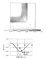
- the stress simulation results are darker (black) in areas where stress is more concentrated.
- the warp was measured diagonally from the electronic component side to the substrate corner side. The same applies to the stress simulation results of the corners and the measurement results of the warpage.
- FIG. 3 is a graph showing the results of corner stress simulation and warpage simulation for a stiffener-equipped wiring board provided with copper stiffeners (conventional stiffeners).
- This copper stiffener (thickness 2.5 mm) has a thermal expansion coefficient of about 17.6 ppm/° C. and is positioned on the upper surface of the wiring board via an adhesive.
- this wiring board with a stiffener is warped, it converges to near 0 at the ends (corners) of the wiring board. Therefore, this wiring board with a stiffener can be mounted on a motherboard in terms of warpage, but in terms of stress, cracks are likely to occur when repeatedly used in high and low temperature environments.
- FIG. 4 is a graph showing the results of corner stress simulation and warp simulation for a wiring board with a stiffener, assuming that the stiffener has a thermal expansion coefficient of 20 ppm/°C (Young's modulus is set to be the same as that of copper). From the results of the stress simulation, the region between the electronic component 7 and the stiffener 6 (edge portion of the stiffener 6) is darker than the result shown in FIG. 3, indicating that the generated stress is more concentrated in this region. Recognize. Also, it can be seen that the wiring board with the stiffener is warped in the opposite direction (positive direction) at the end (corner) of the wiring board. Therefore, this wiring board with stiffeners cannot be mounted on a motherboard.
- FIG. 5 is a graph showing the results of corner stress simulation and warpage simulation for a wiring board with a stiffener, assuming that the stiffener has a thermal expansion coefficient of 15 ppm/°C (Young's modulus is set to be the same as that of copper). From the stress simulation results, it can be seen that the area between the electronic component 7 and the stiffener 6 (edge portion of the stiffener 6) is thinner than the result shown in FIG. 3, and the generated stress is smaller than that in FIG. However, it can be seen that the warpage of the wiring board with the stiffener is larger than that in FIG. 3, and does not converge to near 0 even at the end (corner) of the wiring board.
- this wiring board with stiffeners cannot be mounted on the motherboard. 4 and 5, when the coefficient of thermal expansion of the stiffener is larger than that of copper, the force for correcting the warp is increased, but the stress is increased. Also, it can be seen that if the coefficient of thermal expansion of the stiffener is smaller than that of copper, the stress is reduced, but the correction force against warpage is reduced.
- FIG. 6 is a graph showing the results of corner stress simulation and warpage simulation for a stiffener-equipped wiring board provided with an AlSiC (SiC 40%) stiffener (conventional stiffener).
- This AlSiC (SiC 40%) stiffener (thickness: 2.5 mm) has a thermal expansion coefficient of about 12.4 ppm/° C., and is positioned on the upper surface of the wiring board via an adhesive.
- FIG. 7 is a graph showing the results of corner stress simulation and warpage simulation for a stiffener-equipped wiring board provided with an AlSiC (SiC 45%) stiffener (conventional stiffener).
- This AlSiC (SiC 45%) stiffener (2.5 mm thick) has a thermal expansion coefficient of about 10.5 ppm/° C. and is positioned on the upper surface of the wiring board via solder.
- FIG. 8 is a graph showing corner stress simulation results and warpage simulation results for a stiffener-equipped wiring board having a stiffener with a lower layer of copper and an upper layer of AlSiC (SiC 40%) (a stiffener outside the scope of the present disclosure). is.
- the thermal expansion coefficients of copper and AlSiC (SiC 40%) are given above.
- the stiffener (thickness: 2.5 mm) is positioned on the upper surface of the wiring board with the adhesive between the lower layer and the upper layer.
- FIG. 9 is a graph showing corner stress simulation results and warpage simulation results for a wiring substrate with stiffeners having a stiffener with a lower layer of copper and an upper layer of AlSiC (SiC 45%) (a stiffener outside the scope of the present disclosure). is.
- the thermal expansion coefficients of copper and AlSiC (45% SiC) are given above.
- the stiffener (thickness: 2.5 mm) is positioned on the upper surface of the wiring board with the adhesive between the lower layer and the upper layer.
- FIG. 10 is a graph showing the results of corner stress simulation and warpage simulation for a wiring board with a stiffener having a stiffener (stiffener of the present disclosure) with AlSiC (SiC 40%) as a lower layer and copper as an upper layer.
- the thermal expansion coefficients of copper and AlSiC (SiC 40%) are given above.
- the stiffener (thickness: 2.5 mm) is positioned on the upper surface of the wiring board with the adhesive between the lower layer and the upper layer.
- FIG. 11 is a graph showing the results of corner stress simulation and warpage simulation for a stiffener-equipped wiring board provided with a stiffener (stiffener of the present disclosure) having a lower layer of AlSiC (45% SiC) and an upper layer of copper.
- the thermal expansion coefficients of copper and AlSiC (45% SiC) are given above.
- the stiffener (thickness: 2.5 mm) is soldered between the lower layer and the upper layer, and is located on the upper surface of the wiring board via the solder.
- FIG. 12 is a graph showing the degree of stress relaxation for a stiffener-equipped wiring board with stiffeners (stiffeners of the present disclosure) having a top layer of copper and a bottom layer of AlSiC (SiC 40% and 45%).
- the graph shown in FIG. 12 shows the relative value of the stress generated in the wiring board with stiffener using the stiffener of the present disclosure when the stress generated in the wiring board with stiffener using the stiffener made of copper shown in FIG. showing.
- the use of AlSiC (SiC 45%) which has a smaller coefficient of thermal expansion, reduces the stress more.
- the stress generated in a wiring board with a stiffener provided with a stiffener (stiffener of the present disclosure) having a lower layer of AlSiC (40% SiC) and an upper layer of copper is It is 90% of the generated stress, and it can be seen that the generated stress is reduced by as much as 10%.
- the stress generated in a wiring board with a stiffener having a stiffener (a stiffener of the present disclosure) with AlSiC (SiC 45%) as a lower layer and copper as an upper layer is 85% of the stress generated in a wiring board with a stiffener using a stiffener made of copper. It can be seen that the generated stress is reduced by as much as 15%.
Landscapes
- Engineering & Computer Science (AREA)
- Microelectronics & Electronic Packaging (AREA)
- Manufacturing & Machinery (AREA)
- Structure Of Printed Boards (AREA)
Priority Applications (4)
| Application Number | Priority Date | Filing Date | Title |
|---|---|---|---|
| KR1020247020396A KR20240108500A (ko) | 2021-12-28 | 2022-12-23 | 스티프너 부착 배선 기판 |
| CN202280084771.6A CN118414891A (zh) | 2021-12-28 | 2022-12-23 | 带加强件的布线基板 |
| US18/724,914 US20250106984A1 (en) | 2021-12-28 | 2022-12-23 | Wiring board with stiffener |
| JP2023570960A JP7784446B2 (ja) | 2021-12-28 | 2022-12-23 | スティフナ付き配線基板 |
Applications Claiming Priority (2)
| Application Number | Priority Date | Filing Date | Title |
|---|---|---|---|
| JP2021214992 | 2021-12-28 | ||
| JP2021-214992 | 2021-12-28 |
Publications (1)
| Publication Number | Publication Date |
|---|---|
| WO2023127725A1 true WO2023127725A1 (ja) | 2023-07-06 |
Family
ID=86999232
Family Applications (1)
| Application Number | Title | Priority Date | Filing Date |
|---|---|---|---|
| PCT/JP2022/047631 Ceased WO2023127725A1 (ja) | 2021-12-28 | 2022-12-23 | スティフナ付き配線基板 |
Country Status (6)
| Country | Link |
|---|---|
| US (1) | US20250106984A1 (https=) |
| JP (1) | JP7784446B2 (https=) |
| KR (1) | KR20240108500A (https=) |
| CN (1) | CN118414891A (https=) |
| TW (1) | TWI854415B (https=) |
| WO (1) | WO2023127725A1 (https=) |
Cited By (1)
| Publication number | Priority date | Publication date | Assignee | Title |
|---|---|---|---|---|
| WO2025243527A1 (ja) * | 2024-05-24 | 2025-11-27 | 株式会社レゾナック | 半導体装置 |
Citations (7)
| Publication number | Priority date | Publication date | Assignee | Title |
|---|---|---|---|---|
| JP2001110926A (ja) * | 1999-10-13 | 2001-04-20 | Nec Corp | フリップチップパッケージ |
| JP2004356569A (ja) * | 2003-05-30 | 2004-12-16 | Shinko Electric Ind Co Ltd | 半導体装置用パッケージ |
| JP2005217003A (ja) * | 2004-01-28 | 2005-08-11 | Kyocera Corp | 半導体素子収納用パッケージ |
| WO2006087769A1 (ja) * | 2005-02-15 | 2006-08-24 | Fujitsu Limited | パッケージ実装モジュールおよびパッケージ基板モジュール |
| JP2010103516A (ja) * | 2008-09-29 | 2010-05-06 | Ngk Spark Plug Co Ltd | 補強材付き配線基板 |
| JP2013026633A (ja) * | 2011-07-14 | 2013-02-04 | Toshiba Corp | テレビジョン受像機、及び電子機器 |
| US20200013732A1 (en) * | 2018-02-26 | 2020-01-09 | International Business Machines Corporation | Laminated stiffener to control the warpage of electronic chip carriers |
Family Cites Families (5)
| Publication number | Priority date | Publication date | Assignee | Title |
|---|---|---|---|---|
| US6472762B1 (en) * | 2001-08-31 | 2002-10-29 | Lsi Logic Corporation | Enhanced laminate flipchip package using a high CTE heatspreader |
| JP4599891B2 (ja) | 2004-05-28 | 2010-12-15 | 凸版印刷株式会社 | 半導体装置用基板並びに半導体装置 |
| JP5350829B2 (ja) | 2009-02-16 | 2013-11-27 | 日本特殊陶業株式会社 | 補強材付き配線基板の製造方法、補強材付き配線基板用の配線基板 |
| MY209993A (en) | 2019-02-04 | 2025-08-19 | Sony Interactive Entertainment Inc | Electronic apparatus, semiconductor device, insulating sheet, and method for manufacturing semiconductor device |
| JP7351107B2 (ja) | 2019-06-06 | 2023-09-27 | 凸版印刷株式会社 | 配線基板及び配線基板の製造方法 |
-
2022
- 2022-12-23 JP JP2023570960A patent/JP7784446B2/ja active Active
- 2022-12-23 CN CN202280084771.6A patent/CN118414891A/zh not_active Withdrawn
- 2022-12-23 US US18/724,914 patent/US20250106984A1/en active Pending
- 2022-12-23 KR KR1020247020396A patent/KR20240108500A/ko not_active Withdrawn
- 2022-12-23 WO PCT/JP2022/047631 patent/WO2023127725A1/ja not_active Ceased
- 2022-12-27 TW TW111150174A patent/TWI854415B/zh active
Patent Citations (7)
| Publication number | Priority date | Publication date | Assignee | Title |
|---|---|---|---|---|
| JP2001110926A (ja) * | 1999-10-13 | 2001-04-20 | Nec Corp | フリップチップパッケージ |
| JP2004356569A (ja) * | 2003-05-30 | 2004-12-16 | Shinko Electric Ind Co Ltd | 半導体装置用パッケージ |
| JP2005217003A (ja) * | 2004-01-28 | 2005-08-11 | Kyocera Corp | 半導体素子収納用パッケージ |
| WO2006087769A1 (ja) * | 2005-02-15 | 2006-08-24 | Fujitsu Limited | パッケージ実装モジュールおよびパッケージ基板モジュール |
| JP2010103516A (ja) * | 2008-09-29 | 2010-05-06 | Ngk Spark Plug Co Ltd | 補強材付き配線基板 |
| JP2013026633A (ja) * | 2011-07-14 | 2013-02-04 | Toshiba Corp | テレビジョン受像機、及び電子機器 |
| US20200013732A1 (en) * | 2018-02-26 | 2020-01-09 | International Business Machines Corporation | Laminated stiffener to control the warpage of electronic chip carriers |
Cited By (1)
| Publication number | Priority date | Publication date | Assignee | Title |
|---|---|---|---|---|
| WO2025243527A1 (ja) * | 2024-05-24 | 2025-11-27 | 株式会社レゾナック | 半導体装置 |
Also Published As
| Publication number | Publication date |
|---|---|
| TW202335541A (zh) | 2023-09-01 |
| US20250106984A1 (en) | 2025-03-27 |
| JP7784446B2 (ja) | 2025-12-11 |
| CN118414891A (zh) | 2024-07-30 |
| TWI854415B (zh) | 2024-09-01 |
| JPWO2023127725A1 (https=) | 2023-07-06 |
| KR20240108500A (ko) | 2024-07-09 |
Similar Documents
| Publication | Publication Date | Title |
|---|---|---|
| KR101906883B1 (ko) | 배선 기판 및 그 제조 방법 | |
| JP6302184B2 (ja) | 信頼性のある表面実装集積型パワーモジュール | |
| US8163642B1 (en) | Package substrate with dual material build-up layers | |
| US11139230B2 (en) | Flip-chip package substrate and method for preparing the same | |
| US6317331B1 (en) | Wiring substrate with thermal insert | |
| US9048229B2 (en) | Printed wiring board | |
| JP2016063130A (ja) | プリント配線板および半導体パッケージ | |
| JP6639934B2 (ja) | 配線基板、半導体装置及び配線基板の製造方法 | |
| JP7784446B2 (ja) | スティフナ付き配線基板 | |
| JP2010010329A (ja) | 配線基板およびその製造方法 | |
| US10314166B2 (en) | Printed wiring board | |
| JP7352490B2 (ja) | 配線基板 | |
| US20250185157A1 (en) | Wiring board | |
| US12621928B2 (en) | Wiring board | |
| US20250016912A1 (en) | Wiring board | |
| JP2008251601A (ja) | 半導体装置及びその実装構造 | |
| TW201507565A (zh) | 配線基板 | |
| WO2025142993A1 (ja) | 実装構造体 | |
| TW202539314A (zh) | 配線基板及半導體裝置 | |
| WO2025183114A1 (ja) | 配線基板および半導体デバイス | |
| CN110958762A (zh) | 印刷布线基板 | |
| JPH06196861A (ja) | 多層プリント配線板 | |
| JP2006339175A (ja) | 積層型半導体装置 |
Legal Events
| Date | Code | Title | Description |
|---|---|---|---|
| 121 | Ep: the epo has been informed by wipo that ep was designated in this application |
Ref document number: 22915948 Country of ref document: EP Kind code of ref document: A1 |
|
| WWE | Wipo information: entry into national phase |
Ref document number: 2023570960 Country of ref document: JP |
|
| ENP | Entry into the national phase |
Ref document number: 20247020396 Country of ref document: KR Kind code of ref document: A |
|
| WWE | Wipo information: entry into national phase |
Ref document number: 1020247020396 Country of ref document: KR |
|
| WWE | Wipo information: entry into national phase |
Ref document number: 202280084771.6 Country of ref document: CN |
|
| WWE | Wipo information: entry into national phase |
Ref document number: 18724914 Country of ref document: US |
|
| NENP | Non-entry into the national phase |
Ref country code: DE |
|
| 122 | Ep: pct application non-entry in european phase |
Ref document number: 22915948 Country of ref document: EP Kind code of ref document: A1 |
|
| WWP | Wipo information: published in national office |
Ref document number: 18724914 Country of ref document: US |