WO2023127643A1 - 積層セラミックコンデンサ - Google Patents
積層セラミックコンデンサ Download PDFInfo
- Publication number
- WO2023127643A1 WO2023127643A1 PCT/JP2022/047111 JP2022047111W WO2023127643A1 WO 2023127643 A1 WO2023127643 A1 WO 2023127643A1 JP 2022047111 W JP2022047111 W JP 2022047111W WO 2023127643 A1 WO2023127643 A1 WO 2023127643A1
- Authority
- WO
- WIPO (PCT)
- Prior art keywords
- layer
- internal electrode
- dielectric
- layers
- ceramic capacitor
- Prior art date
- Legal status (The legal status is an assumption and is not a legal conclusion. Google has not performed a legal analysis and makes no representation as to the accuracy of the status listed.)
- Ceased
Links
Images

Classifications
-
- H—ELECTRICITY
- H01—ELECTRIC ELEMENTS
- H01G—CAPACITORS; CAPACITORS, RECTIFIERS, DETECTORS, SWITCHING DEVICES, LIGHT-SENSITIVE OR TEMPERATURE-SENSITIVE DEVICES OF THE ELECTROLYTIC TYPE
- H01G4/00—Fixed capacitors; Processes of their manufacture
- H01G4/002—Details
- H01G4/005—Electrodes
- H01G4/008—Selection of materials
- H01G4/0085—Fried electrodes
-
- H—ELECTRICITY
- H01—ELECTRIC ELEMENTS
- H01G—CAPACITORS; CAPACITORS, RECTIFIERS, DETECTORS, SWITCHING DEVICES, LIGHT-SENSITIVE OR TEMPERATURE-SENSITIVE DEVICES OF THE ELECTROLYTIC TYPE
- H01G4/00—Fixed capacitors; Processes of their manufacture
- H01G4/002—Details
- H01G4/005—Electrodes
- H01G4/008—Selection of materials
-
- H—ELECTRICITY
- H01—ELECTRIC ELEMENTS
- H01G—CAPACITORS; CAPACITORS, RECTIFIERS, DETECTORS, SWITCHING DEVICES, LIGHT-SENSITIVE OR TEMPERATURE-SENSITIVE DEVICES OF THE ELECTROLYTIC TYPE
- H01G4/00—Fixed capacitors; Processes of their manufacture
- H01G4/002—Details
- H01G4/005—Electrodes
- H01G4/012—Form of non-self-supporting electrodes
-
- H—ELECTRICITY
- H01—ELECTRIC ELEMENTS
- H01G—CAPACITORS; CAPACITORS, RECTIFIERS, DETECTORS, SWITCHING DEVICES, LIGHT-SENSITIVE OR TEMPERATURE-SENSITIVE DEVICES OF THE ELECTROLYTIC TYPE
- H01G4/00—Fixed capacitors; Processes of their manufacture
- H01G4/002—Details
- H01G4/018—Dielectrics
- H01G4/06—Solid dielectrics
- H01G4/08—Inorganic dielectrics
- H01G4/12—Ceramic dielectrics
-
- H—ELECTRICITY
- H01—ELECTRIC ELEMENTS
- H01G—CAPACITORS; CAPACITORS, RECTIFIERS, DETECTORS, SWITCHING DEVICES, LIGHT-SENSITIVE OR TEMPERATURE-SENSITIVE DEVICES OF THE ELECTROLYTIC TYPE
- H01G4/00—Fixed capacitors; Processes of their manufacture
- H01G4/002—Details
- H01G4/018—Dielectrics
- H01G4/06—Solid dielectrics
- H01G4/08—Inorganic dielectrics
- H01G4/12—Ceramic dielectrics
- H01G4/1209—Ceramic dielectrics characterised by the ceramic dielectric material
-
- H—ELECTRICITY
- H01—ELECTRIC ELEMENTS
- H01G—CAPACITORS; CAPACITORS, RECTIFIERS, DETECTORS, SWITCHING DEVICES, LIGHT-SENSITIVE OR TEMPERATURE-SENSITIVE DEVICES OF THE ELECTROLYTIC TYPE
- H01G4/00—Fixed capacitors; Processes of their manufacture
- H01G4/002—Details
- H01G4/018—Dielectrics
- H01G4/06—Solid dielectrics
- H01G4/08—Inorganic dielectrics
- H01G4/12—Ceramic dielectrics
- H01G4/1209—Ceramic dielectrics characterised by the ceramic dielectric material
- H01G4/1218—Ceramic dielectrics characterised by the ceramic dielectric material based on titanium oxides or titanates
- H01G4/1227—Ceramic dielectrics characterised by the ceramic dielectric material based on titanium oxides or titanates based on alkaline earth titanates
-
- H—ELECTRICITY
- H01—ELECTRIC ELEMENTS
- H01G—CAPACITORS; CAPACITORS, RECTIFIERS, DETECTORS, SWITCHING DEVICES, LIGHT-SENSITIVE OR TEMPERATURE-SENSITIVE DEVICES OF THE ELECTROLYTIC TYPE
- H01G4/00—Fixed capacitors; Processes of their manufacture
- H01G4/002—Details
- H01G4/228—Terminals
- H01G4/232—Terminals electrically connecting two or more layers of a stacked or rolled capacitor
-
- H—ELECTRICITY
- H01—ELECTRIC ELEMENTS
- H01G—CAPACITORS; CAPACITORS, RECTIFIERS, DETECTORS, SWITCHING DEVICES, LIGHT-SENSITIVE OR TEMPERATURE-SENSITIVE DEVICES OF THE ELECTROLYTIC TYPE
- H01G4/00—Fixed capacitors; Processes of their manufacture
- H01G4/002—Details
- H01G4/228—Terminals
- H01G4/232—Terminals electrically connecting two or more layers of a stacked or rolled capacitor
- H01G4/2325—Terminals electrically connecting two or more layers of a stacked or rolled capacitor characterised by the material of the terminals
-
- H—ELECTRICITY
- H01—ELECTRIC ELEMENTS
- H01G—CAPACITORS; CAPACITORS, RECTIFIERS, DETECTORS, SWITCHING DEVICES, LIGHT-SENSITIVE OR TEMPERATURE-SENSITIVE DEVICES OF THE ELECTROLYTIC TYPE
- H01G4/00—Fixed capacitors; Processes of their manufacture
- H01G4/30—Stacked capacitors
-
- Y—GENERAL TAGGING OF NEW TECHNOLOGICAL DEVELOPMENTS; GENERAL TAGGING OF CROSS-SECTIONAL TECHNOLOGIES SPANNING OVER SEVERAL SECTIONS OF THE IPC; TECHNICAL SUBJECTS COVERED BY FORMER USPC CROSS-REFERENCE ART COLLECTIONS [XRACs] AND DIGESTS
- Y02—TECHNOLOGIES OR APPLICATIONS FOR MITIGATION OR ADAPTATION AGAINST CLIMATE CHANGE
- Y02E—REDUCTION OF GREENHOUSE GAS [GHG] EMISSIONS, RELATED TO ENERGY GENERATION, TRANSMISSION OR DISTRIBUTION
- Y02E60/00—Enabling technologies; Technologies with a potential or indirect contribution to GHG emissions mitigation
- Y02E60/13—Energy storage using capacitors
Definitions
- the present invention relates to a multilayer ceramic capacitor.
- a multilayer ceramic capacitor is known in which a plurality of dielectric layers made of a ceramic material and a plurality of internal electrode layers are laminated. Further miniaturization, higher capacity, and improved reliability are required for such multilayer ceramic capacitors. Therefore, attempts have been made to reduce the thickness of the dielectric layers, to reduce the thickness of the internal electrode layers, and to increase the number of these layers laminated.
- Patent Document 1 discloses a problem that short-circuit failure occurs between internal electrode layers when dielectric layers are thinned.
- Patent Literature 1 discloses an invention that solves this problem and suppresses deterioration in reliability by including a conductive layer between internal electrode layers.
- a plurality of through holes are formed in the internal electrode layers.
- Each of the plurality of through-holes is filled with a portion of the adjacent dielectric layer, and it appears that the adjacent dielectric layers are connected. It is called a dielectric connection. If a dielectric connection is formed in the internal electrode layer, the life, ie reliability, of the multilayer ceramic capacitor may be reduced.
- An object of the present invention is to provide a multilayer ceramic capacitor that suppresses deterioration in reliability.
- the inventors of the present application have found that electric field concentration occurs in the dielectric connecting portions formed in the internal electrode layers, and as a result, the service life, that is, the reliability, of the multilayer ceramic capacitor is reduced. obtained new knowledge.
- the inventors of the present application have found that a solid solution in which a metal different from the main component metal of the internal electrode layers, such as Ni, is solid-solved at the interface between the dielectric connecting portion and the internal electrode layers, such as Sn.
- a new finding was obtained that the formation of the layers suppresses the concentration of the electric field and, as a result, suppresses the deterioration of the life, ie reliability, of the multilayer ceramic capacitor.
- a laminated ceramic capacitor according to the present invention is a laminated ceramic capacitor in which a plurality of dielectric layers made of a ceramic material and a plurality of internal electrode layers are laminated, wherein each of the plurality of internal electrode layers is a first and each of the plurality of internal electrode layers is filled with a portion of the adjacent dielectric layer penetrating in the stacking direction to connect the adjacent dielectric layers.
- a plurality of dielectric connecting portions are formed, and a solid solution layer in which a second metal different from the first metal is solid-dissolved is formed at an interface between the dielectric connecting portion and the internal electrode layer.
- the content of the second metal in the solid solution layer is 0.1 mol % or more and 10 mol % or less with respect to 100 mol of the first metal.
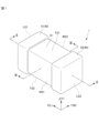
- FIG. 1 is a perspective view showing a laminated ceramic capacitor according to this embodiment
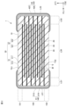
- FIG. FIG. 2 is a sectional view (LT section) taken along the line II-II of the multilayer ceramic capacitor shown in FIG. 1
- FIG. 2 is a sectional view (WT section) taken along line III-III of the multilayer ceramic capacitor shown in FIG. 1
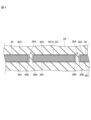
- 3 is an enlarged cross-sectional view of the IV portion of the multilayer ceramic capacitor shown in FIG. 2
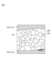
- FIG. FIG. 3 is an enlarged cross-sectional view of a V portion of the multilayer ceramic capacitor shown in FIG. 2;
- FIG. 1 is a perspective view showing a laminated ceramic capacitor according to the present embodiment
- FIG. 2 is a sectional view taken along line II-II of the laminated ceramic capacitor shown in FIG. 1, and FIG. It is the III-III line sectional view of a capacitor.
- a laminated ceramic capacitor 1 shown in FIGS. 1 to 3 includes a laminated body 10 and external electrodes 40 .
- External electrode 40 includes a first external electrode 41 and a second external electrode 42 .
- the X direction is the length direction L of the multilayer ceramic capacitor 1 and the multilayer body 10
- the Y direction is the width direction W of the multilayer ceramic capacitor 1 and the multilayer body 10
- the Z direction is the lamination of the multilayer ceramic capacitor 1 and the multilayer body 10.
- direction T. 2 is also called the LT section
- the section shown in FIG. 3 is also called the WT section.
- length direction L, width direction W, and stacking direction T are not necessarily orthogonal to each other, and may intersect each other.
- the laminate 10 has a substantially rectangular parallelepiped shape, and includes a first main surface TS1 and a second main surface TS2 facing in the lamination direction T, and a first side surface WS1 and a second side surface WS2 facing in the width direction W. , a first end surface LS1 and a second end surface LS2 facing each other in the length direction L. As shown in FIG.
- a corner is a portion where three surfaces of the laminate 10 intersect, and a ridge is a portion where two surfaces of the laminate 10 intersect.
- the laminate 10 has a plurality of dielectric layers 20 and a plurality of internal electrode layers 30 laminated in the lamination direction T. As shown in FIGS. In addition, the laminate 10 has, in the stacking direction T, an inner layer portion 100, and a first outer layer portion 101 and a second outer layer portion 102 which are arranged to sandwich the inner layer portion 100 therebetween.
- the inner layer section 100 includes a portion of the multiple dielectric layers 20 and multiple internal electrode layers 30 .
- a plurality of internal electrode layers 30 are arranged facing each other with the dielectric layers 20 interposed therebetween.
- the inner layer portion 100 is a portion that generates capacitance and substantially functions as a capacitor.
- the first outer layer portion 101 is arranged on the first main surface TS1 side of the laminate 10, and the second outer layer portion 102 is arranged on the second main surface TS2 side of the laminate 10. More specifically, the first outer layer portion 101 is arranged between the internal electrode layer 30 closest to the first main surface TS1 among the plurality of internal electrode layers 30 and the first main surface TS1. , the second outer layer portion 102 is arranged between the internal electrode layer 30 closest to the second main surface TS2 among the plurality of internal electrode layers 30 and the second main surface TS2.
- the first outer layer portion 101 and the second outer layer portion 102 do not include the internal electrode layer 30, and include portions of the plurality of dielectric layers 20 other than the portion for the inner layer portion 100, respectively.
- the first outer layer portion 101 and the second outer layer portion 102 are portions that function as protective layers for the inner layer portion 100 .
- a dielectric ceramic containing BaTiO 3 , CaTiO 3 , SrTiO 3 , CaZrO 3 or the like as a main component can be used.
- a Mn compound, an Fe compound, a Cr compound, a Co compound, a Ni compound, or the like may be added as an accessory component.
- the thickness of the dielectric layer 20 is not particularly limited, it is preferably 0.40 ⁇ m or more and 0.50 ⁇ m or less, more preferably 0.40 ⁇ m or more and 0.45 ⁇ m or less.
- the number of dielectric layers 20 is not particularly limited, but is preferably 100 or more and 2000 or less, for example.
- the number of dielectric layers 20 is the total number of dielectric layers in the inner layer portion and the number of dielectric layers in the outer layer portion.
- the multiple internal electrode layers 30 include multiple first internal electrode layers 31 and multiple second internal electrode layers 32 .
- the plurality of first internal electrode layers 31 and the plurality of second internal electrode layers 32 are alternately arranged in the stacking direction T of the stack 10 .
- the first internal electrode layer 31 includes a counter electrode portion 311 and a lead electrode portion 312
- the second internal electrode layer 32 includes a counter electrode portion 321 and a lead electrode portion 322 .
- the counter electrode portion 311 and the counter electrode portion 321 face each other in the stacking direction T of the laminate 10 with the dielectric layer 20 interposed therebetween.
- the shape of the counter electrode portion 311 and the counter electrode portion 321 is not particularly limited, and may be, for example, a substantially rectangular shape.
- the counter electrode portion 311 and the counter electrode portion 321 are portions that generate capacitance and substantially function as capacitors.
- the extraction electrode portion 312 extends from the counter electrode portion 311 toward the first end face LS1 of the laminate 10 and is exposed at the first end face LS1.
- the extraction electrode portion 322 extends from the counter electrode portion 321 toward the second end surface LS2 of the laminate 10 and is exposed at the second end surface LS2.
- the shape of the extraction electrode portion 312 and the extraction electrode portion 322 is not particularly limited, and may be, for example, a substantially rectangular shape.
- the first internal electrode layer 31 is connected to the first external electrode 41, and the first internal electrode layer 31 and the second end face LS2 of the laminate 10, that is, the second external electrode 42, are connected.
- the second internal electrode layer 32 is connected to the second external electrode 42, and between the second internal electrode layer 32 and the first end surface LS1 of the laminate 10, that is, the first external electrode 41, there is a gap in
- the first internal electrode layer 31 and the second internal electrode layer 32 contain metal Ni as a main component.
- the first internal electrode layer 31 and the second internal electrode layer 32 are formed of metals such as Cu, Ag, Pd, or Au, or alloys containing at least one of these metals, such as Ag—Pd alloys. , may be included as a main component, or may be included as a component other than the main component.
- the first internal electrode layer 31 and the second internal electrode layer 32 may contain dielectric particles having the same composition as the ceramic contained in the dielectric layer 20 as a component other than the main component.
- the metal of the main component is defined as the metal component with the highest weight percentage.
- the thickness of the first internal electrode layer 31 and the second internal electrode layer 32 is not particularly limited, but is preferably 0.30 ⁇ m or more and 0.40 ⁇ m or less, and preferably 0.30 ⁇ m or more and 0.35 ⁇ m or less. more preferred.
- the number of the first internal electrode layers 31 and the second internal electrode layers 32 is not particularly limited, but is preferably 10 or more and 1000 or less.
- the laminate 10 includes, in the width direction W, an electrode facing portion W30 facing the internal electrode layers 30, and a first side gap portion WG1 and a first side gap portion WG1 arranged to sandwich the electrode facing portion W30. 2 side gap portions WG2.
- the first side gap portion WG1 is located between the electrode facing portion W30 and the first side surface WS1
- the second side gap portion WG2 is located between the electrode facing portion W30 and the second side surface WS2. do.
- first side gap portion WG1 is located between the end of the internal electrode layer 30 on the side of the first side surface WS1 and the first side surface WS1
- second side gap portion WG2 is It is located between the end of the internal electrode layer 30 on the side of the second side surface WS2 and the second side surface WS2.
- the first side gap portion WG1 and the second side gap portion WG2 do not include the internal electrode layers 30, and include only the dielectric layers 20.
- the first side gap portion WG1 and the second side gap portion WG2 are portions that function as protective layers for the internal electrode layers 30 .
- the first side gap portion WG1 and the second side gap portion WG2 are also referred to as W gaps.
- the laminate 10 includes, in the length direction L, an electrode facing portion L30 where the first internal electrode layer 31 and the second internal electrode layer 32 of the internal electrode layer 30 face each other, and a first end gap portion LG1 and a second end gap portion LG2.
- the first end gap portion LG1 is located between the electrode facing portion L30 and the first end surface LS1
- the second end gap portion LG2 is located between the electrode facing portion L30 and the second end surface LS2. do. More specifically, the first end gap portion LG1 is located between the end of the second internal electrode layer 32 on the side of the first end surface LS1 and the first end surface LS1.
- LG2 is located between the end of the first internal electrode layer 31 on the second end surface LS2 side and the second end surface LS2.
- the first end gap portion LG1 does not include the second internal electrode layer 32 and includes the first internal electrode layer 31 and the dielectric layer 20, and the second end gap portion LG2 includes the first internal electrode layer 31 and the dielectric layer 20. 31 but includes the second internal electrode layer 32 and the dielectric layer 20 .
- the first end gap portion LG1 is a portion that functions as a lead electrode portion to the first end surface LS1 of the first internal electrode layer 31, and the second end gap portion LG2 is a portion that functions as the second internal electrode layer 32. This is a portion that functions as a lead-out electrode portion to the second end surface LS2 of the .
- the first end gap portion LG1 and the second end gap portion LG2 are also called L gaps.
- the counter electrode portion 311 of the first internal electrode layer 31 and the counter electrode portion 321 of the second internal electrode layer 32 are positioned in the electrode facing portion L30. Further, the extraction electrode portion 312 of the first internal electrode layer 31 described above is located in the first end gap portion LG1, and the extraction electrode portion 312 of the second internal electrode layer 32 described above is located in the second end gap portion LG2. An extraction electrode portion 322 is located.
- the thickness in the stacking direction T is preferably 0.10 mm or more and 0.50 mm or less.
- each value may be an average value of measured values at a plurality of locations in the length direction, or may be an average value of measured values at a plurality of locations in the stacking direction.
- each value may be an average value of measured values at a plurality of locations in the length direction or width direction.
- a method of measuring the length of the laminate 10 for example, there is a method of observing the LT cross section near the center in the width direction of the laminate exposed by polishing with a scanning electron microscope.
- each value may be an average value of measured values at a plurality of locations in the stacking direction.
- each value may be an average value of measured values at a plurality of locations in the stacking direction.
- the external electrode 40 includes a first external electrode 41 and a second external electrode 42 .
- the first external electrode 41 is arranged on the first end surface LS1 of the laminate 10 and connected to the first internal electrode layer 31 .
- the first external electrode 41 may extend from the first end surface LS1 to part of the first main surface TS1 and part of the second main surface TS2. Also, the first external electrode 41 may extend from the first end surface LS1 to a portion of the first side surface WS1 and a portion of the second side surface WS2.
- the second external electrode 42 is arranged on the second end face LS2 of the laminate 10 and connected to the second internal electrode layer 32 .
- the second external electrode 42 may extend from the second end surface LS2 to part of the first principal surface TS1 and part of the second principal surface TS2. Also, the second external electrode 42 may extend from the second end surface LS2 to a portion of the first side surface WS1 and a portion of the second side surface WS2.
- the first external electrode 41 has a first underlying electrode layer 415 and a first plating layer 416
- the second external electrode 42 has a second underlying electrode layer 425 and a second plating layer 426.
- the first external electrode 41 may be composed of the first plated layer 416 only
- the second external electrode 42 may be composed of the second plated layer 426 only.
- the first base electrode layer 415 and the second base electrode layer 425 may be fired layers containing metal and glass.
- glass include glass components containing at least one selected from B, Si, Ba, Mg, Al, Li, and the like.
- borosilicate glass can be used.
- the metal contains Cu as a main component.
- the metal may contain at least one selected from metals such as Ni, Ag, Pd, or Au, or alloys such as Ag—Pd alloys as a main component, or may contain as a component other than the main component. It's okay.
- the sintered layer is a layer obtained by applying a conductive paste containing metal and glass to the laminate by a dip method and then sintering it.
- the firing may be performed after firing the internal electrode layers, or may be performed simultaneously with the firing of the internal electrode layers. Also, the fired layer may be a plurality of layers.
- the first base electrode layer 415 and the second base electrode layer 425 may be resin layers containing conductive particles and thermosetting resin.
- the resin layer may be formed on the fired layer described above, or may be formed directly on the laminate without forming the fired layer.
- the resin layer is a layer obtained by applying a conductive paste containing conductive particles and a thermosetting resin to the laminate by a coating method and firing the layer.
- the firing may be performed after firing the internal electrode layers, or may be performed simultaneously with the firing of the internal electrode layers.
- the resin layer may be a plurality of layers.
- each layer of the first base electrode layer 415 and the second base electrode layer 425 as the fired layer or resin layer is not particularly limited, and may be 1 ⁇ m or more and 10 ⁇ m or less.
- the first base electrode layer 415 and the second base electrode layer 425 may be thin film layers of 1 ⁇ m or less formed by a thin film forming method such as a sputtering method or a vapor deposition method and having metal particles deposited thereon.
- the first plating layer 416 covers at least part of the first base electrode layer 415
- the second plating layer 426 covers at least part of the second base electrode layer 425 .
- the first plating layer 416 and the second plating layer 426 contain at least one selected from metals such as Cu, Ni, Ag, Pd, and Au, and alloys such as Ag—Pd alloys, for example.
- Each of the first plating layer 416 and the second plating layer 426 may be formed of multiple layers.
- a two-layer structure of Ni plating and Sn plating is preferred.
- the Ni plating layer can prevent the base electrode layer from being eroded by solder when mounting the ceramic electronic component, and the Sn plating layer improves the wettability of the solder when mounting the ceramic electronic component. , can be easily implemented.
- each layer of the first plating layer 416 and the second plating layer 426 is not particularly limited, and may be 1 ⁇ m or more and 10 ⁇ m or less.
- FIG. 4 is an enlarged cross-sectional view of the IV portion of the multilayer ceramic capacitor shown in FIG.
- the through-holes 30A are filled with a portion of the adjacent dielectric layers 20 and 20 and appear to be connected to the adjacent dielectric layers 20 and 20.
- the through-holes are referred to as dielectric connecting portions 30A.
- each of the internal electrode layers 30 is formed with a plurality of dielectric coupling portions 30A.
- the dielectric connecting portion 30A is formed in the internal electrode layer 30, electric field concentration occurs at the dielectric connecting portion 30A, and the life, ie reliability, of the multilayer ceramic capacitor 1 may be reduced.
- a solid-solution layer in which the main component metal of the internal electrode layer 30, such as Ni, and the subcomponent metal, such as Sn, are segregated and solid-solved. 30B are formed.
- a solid solution layer 30B is formed at the interface between the internal electrode layer 30 and the dielectric connecting portion 30A.
- Sn segregates and forms a solid solution.
- At least one of Sn, In, Ga, Zn, Bi, Pb, Fe, V, Y, and Cu may be used as the metal that dissolves in the solid solution layer 30B.
- the insulating properties are improved in the vicinity of the edge of the dielectric connecting portion 30A where the solid-solution layer 30B is formed. Concentration of the electric field can be suppressed in the body connecting portion 30A. Therefore, it is possible to suppress the deterioration of the life of the multilayer ceramic capacitor 1, that is, the reliability.
- the content (molar ratio) of the subcomponent metal such as Sn in the solid solution layer 30B is preferably 0.1 mol % or more and 10 mol % or less with respect to 100 mol of the main component metal of the internal electrode layer 30, such as Ni. It is more preferably 0.2 mol % or more and 2.5 mol % or less.
- the content of the subcomponent metal such as Sn in the solid solution layer 30B is less than 0.1 mol%, the above effect of containing the subcomponent metal such as Sn is small.
- the content of the subcomponent metal such as Sn in the solid solution layer 30B exceeds 10 mol %, the melting point of the internal electrode layer 30 is lowered, and the main component metal of the internal electrode layer 30, such as Ni, is beaded.
- the main component metal for example Ni
- the internal electrode layer 30 locally thickens
- the dielectric layer 20 locally thins
- the electric field strength The effect of containing the component metal is canceled.
- the content mol % (molar ratio) of the subcomponent metal such as Sn in the solid solution layer 30B with respect to 100 mol of the main component metal in the internal electrode layer 30, for example, Ni, the central portion in the stacking direction T, the width direction W This is a value obtained by measuring 10 points of the interface at the central portion and the central portion in the length direction L by TEM analysis and averaging the values.
- one or more dielectric connection portions 30A are formed per 100 ⁇ m per internal electrode layer 30 .
- a method for measuring the number of dielectric connection portions 30A an image is taken with an optical microscope or an SEM at a viewing angle at which internal electrodes of 100 ⁇ m or more are included, and images are taken at equal intervals in three fields of view in the stacking direction.
- the number of dielectric connecting portions 30A is measured for each field of view, and the number of the three fields of view is averaged to find the average number.
- the average value of the number of dielectric connection portions 30A in the three fields of view of the desired internal electrode layer 30 is taken as the average number of dielectric connection portions 30A of the plurality of internal electrode layers 30 of the multilayer ceramic capacitor 1 .
- the thickness of the solid solution layer 30B is preferably 1 nm or more and 20 nm or less.
- the method for measuring the thickness of the solid solution layer 30B is not particularly limited. An example using electron microscopy (TEM) is given below.
- the dielectric layers 20 are electrolytically stripped from desired internal electrode layers 30 in the vicinity of the center in the stacking direction T of the stack 10 .
- the peeling part in the lamination direction T of the laminated body 10 is not limited to this. Using, for example, SEM-EDX, three fields of view each having a size of, for example, 50 ⁇ m ⁇ 50 ⁇ m are imaged near the center of the desired internal electrode layer 30 .
- the image pick-up location in the plane of the internal electrode layer 30 and the size of the field of view are not limited to these.
- measure the thickness of each of the solid solution layers 30B of subcomponent metal such as Sn in the vicinity of the dielectric coupling portion 30A average the thickness of all the solid solution layers 30B for each field of view, and The thickness of the field is averaged to obtain the average thickness.
- the average thickness of the solid solution layers 30B in the three fields of view of the desired internal electrode layers 30 is taken as the average thickness of the solid solution layers 30B of the plurality of internal electrode layers 30 of the multilayer ceramic capacitor 1 .
- the solid solution layer 30B preferably covers at least 75% or more of the periphery of the dielectric connecting portion 30A.
- the method for measuring the coverage of the solid solution layer 30B is not particularly limited, but for example, wavelength dispersive X-ray analysis (WDX) or energy dispersive X-ray analysis (EDX), scanning electron microscope (SEM) or transmission type An example using electron microscopy (TEM) is given below.
- the dielectric layers 20 are electrolytically stripped from desired internal electrode layers 30 in the vicinity of the center in the stacking direction T of the stack 10 .
- the peeling part in the lamination direction T of the laminated body 10 is not limited to this.
- the image pick-up location in the plane of the internal electrode layer 30 and the size of the field of view are not limited to these.
- measure the coverage of each of the solid solution layers 30B of subcomponent metal such as Sn in the vicinity of the dielectric coupling portion 30A average the coverage of all the solid solution layers 30B for each field of view, and The coverage of the field of view is averaged to obtain the average coverage.
- the average value of the coverage of the solid solution layers 30B in the three fields of view of the desired internal electrode layers 30 is taken as the average coverage of the solid solution layers 30B of the plurality of internal electrode layers 30 of the multilayer ceramic capacitor 1 .
- the thinning of the dielectric layer 20 may increase the strength of the electric field applied per layer, reducing the life, ie reliability, of the multilayer ceramic capacitor 1 .
- a solid-solution layer 30C may be formed at the boundary between the dielectric layer 20 and the internal electrode layer 30 as well, in which a subcomponent metal such as Sn is segregated and solid-solved.
- a solid-solution layer 30C of a subcomponent metal such as Sn may be formed also at the interface between the internal electrode layer 30 and the dielectric layer 20 .
- the content of the subcomponent metal such as Sn in the solid solution layer 30B is higher than the content of the subcomponent metal such as Sn in the solid solution layer 30C.
- dielectric layer 20 When the solid-solution layer 30C of a subcomponent metal such as Sn is formed at the interface with the dielectric layer 20, the insulating properties at the interface with the dielectric layer 20 on which the solid-solution layer 30C is formed are improved. At 20, an increase in electric field strength can be suppressed. Therefore, it is possible to suppress the deterioration of the life of the multilayer ceramic capacitor 1, that is, the reliability. ⁇ dielectric layer>> Next, the dielectric layer 20 will be further described. 5 is an enlarged cross-sectional view of the V portion of the multilayer ceramic capacitor shown in FIG. 2. FIG. As shown in FIG. 5, dielectric layer 20 includes a plurality of dielectric grains 20A.
- the dielectric grains 20A are, as described above, barium titanate-based ceramics such as perovskite compounds containing Ba and Ti.
- the dielectric grains 20A may contain at least one of La, Ce, Pr, Nd, Sm, Eu, Gd, Tb, Dy, Ho, Er, Tm, Yb, Lu and Y as an accessory component.
- the above-described auxiliary component metal such as Sn may be solid-dissolved at the interfaces 20B of the dielectric grains 20A.
- a method for manufacturing the laminated ceramic capacitor 1 described above will be described.
- the dielectric sheet contains Sn.
- an insulator sheet containing core-shell structure dielectric grain particles coated on the surface with Sn is used.
- the dielectric sheet and the conductive paste contain a binder and a solvent. Known materials can be used as the binder and solvent.
- an internal electrode pattern is formed on the dielectric sheet by printing a conductive paste on the dielectric sheet, for example, in a predetermined pattern.
- a method for forming the internal electrode pattern screen printing, gravure printing, or the like can be used.
- a predetermined number of dielectric sheets for the second outer layer portion 102 on which the internal electrode pattern is not printed are laminated.
- Dielectric sheets for the inner layer section 100 on which the internal electrode pattern is printed are successively laminated thereon.
- a predetermined number of dielectric sheets for the first outer layer section 101 on which the internal electrode pattern is not printed are laminated thereon. Thereby, a laminated sheet is produced.
- the laminated sheet is pressed in the lamination direction by means of isostatic pressing or the like to produce a laminated block.
- the laminated block is cut into a predetermined size to cut out laminated chips. At this time, the corners and ridges of the laminated chips are rounded by barrel polishing or the like.
- the firing temperature is preferably 900° C. or more and 1400° C. or less, although it depends on the materials of the dielectric and internal electrodes.
- a plurality of dielectric connecting portions 30A are formed in the internal electrode layers 30, and Sn derived from the dielectric layers 20 is segregated and solid-dissolved at the interfaces between the dielectric connecting portions 30A and the internal electrode layers 30.
- a solution layer 30B is formed.
- a solid solution layer 30C may be formed in which Sn derived from the dielectric layer 20 is segregated and dissolved. Further, Sn may remain at the interfaces 20B of the dielectric grains 20A of the dielectric layer 20, that is, Sn may segregate and form a solid solution.
- the first base electrode layer 415 is formed on the first end face LS1.
- a second base electrode layer 425 is formed on the second end face LS2.
- the firing temperature is preferably 600° C. or higher and 900° C. or lower.
- the first base electrode layer 415 and the second base electrode layer 415 which are resin layers, are formed by applying a conductive paste containing conductive particles and a thermosetting resin by a coating method and baking the paste.
- the layer 425 may be formed, or the first base electrode layer 415 and the second base electrode layer 425 which are thin films may be formed by a thin film formation method such as a sputtering method or an evaporation method.
- a first plated layer 416 is formed on the surface of the first base electrode layer 415 to form the first external electrode 41, and a second plated layer 426 is formed on the surface of the second base electrode layer 425. Then, the second external electrodes 42 are formed.
- the laminated ceramic capacitor 1 described above is obtained.
- a plurality of dielectric coupling portions 30A are formed in the internal electrode layers 30 by thinning the internal electrode layers 30, for example.
- a solid-solution layer 30B is formed in which a main component metal of the internal electrode layer 30, such as Ni, and a subcomponent metal, such as Sn, are solid-dissolved.
- the insulating properties are improved in the vicinity of the edge of the dielectric connecting portion 30A where the solid solution layer 30B is formed, and the concentration of the electric field in the dielectric connecting portion 30A can be suppressed. Therefore, it is possible to suppress the deterioration of the life of the multilayer ceramic capacitor 1, that is, the reliability.
- the multilayer ceramic capacitor 1 of the present embodiment even if the interface between the internal electrode layer 30 and the dielectric layer 20 is formed with a solid-solution layer 30C in which a subcomponent metal, for example, Sn is dissolved, good.
- the content of the subcomponent metal such as Sn in the solid solution layer 30B is higher than the content of the subcomponent metal such as Sn in the solid solution layer 30C. This improves the insulation at the interface with the dielectric layer 20 on which the solid solution layer 30C is formed, and can suppress an increase in the electric field intensity due to the thinning of the dielectric layer 20, for example. Therefore, it is possible to suppress the deterioration of the life of the multilayer ceramic capacitor 1, that is, the reliability.
- a method of manufacturing a multilayer ceramic capacitor a method of applying a dielectric to the side gaps on the side surfaces WS1 and WS2 in the width direction W of the multilayer body 10 afterward may be applied.
- both ends of the internal electrode layers in the width direction W are aligned (with an error of 5 ⁇ m, for example).
Landscapes
- Engineering & Computer Science (AREA)
- Power Engineering (AREA)
- Manufacturing & Machinery (AREA)
- Microelectronics & Electronic Packaging (AREA)
- Chemical & Material Sciences (AREA)
- Ceramic Engineering (AREA)
- Inorganic Chemistry (AREA)
- Materials Engineering (AREA)
- Fixed Capacitors And Capacitor Manufacturing Machines (AREA)
- Ceramic Capacitors (AREA)
Abstract
Description
図1は、本実施形態に係る積層セラミックコンデンサを示す斜視図であり、図2は、図1に示す積層セラミックコンデンサのII-II線断面図であり、図3は、図1に示す積層セラミックコンデンサのIII-III線断面図である。図1~図3に示す積層セラミックコンデンサ1は、積層体10と外部電極40とを備える。外部電極40は、第1の外部電極41と第2の外部電極42とを含む。
同様に、積層体10の長さの測定方法としては、例えば研磨により露出させた積層体の幅方向中央近傍のLT断面を走査型電子顕微鏡にて観察する方法が挙げられる。また、各値は、積層方向の複数個所の測定値の平均値であってもよい。
同様に、積層体10の幅の測定方法としては、例えば研磨により露出させた積層体の長さ方向中央近傍のWT断面を走査型電子顕微鏡にて観察する方法が挙げられる。また、各値は、積層方向の複数個所の測定値の平均値であってもよい。
次に、内部電極層30、すなわち第1の内部電極層31および第2の内部電極層32、について更に説明する。図4は、図2に示す積層セラミックコンデンサのIV部分の拡大断面図である。例えば内部電極層30の薄膜化により、図4に示すように、内部電極層30、すなわち第1の内部電極層31および第2の内部電極層32、の各々には、積層方向に貫通する複数の貫通孔30Aが形成される。貫通孔30Aには、隣接する誘電体層20および20の一部が充填され、隣接する誘電体層20および20が連結されるようにみえることから、本出願では、内部電極層30に形成される貫通孔を誘電体連結部30Aと称する。換言すれば、内部電極層30の各々には、複数の誘電体連結部30Aが形成されている。
・積層体10の積層方向Tの中央近傍において、所望の内部電極層30から誘電体層20を電解剥離する。なお、積層体10の積層方向Tにおける剥離箇所はこれに限定されない。
・例えばSEM-EDXを用いて、所望の内部電極層30の面内中央近傍において、例えば50μm×50μmの大きさの3視野を撮像する。なお、内部電極層30の面内における撮像箇所、視野の大きさはこれに限定されない。
・撮像された画像において、誘電体連結部30A近傍のSn等の副成分金属の固溶層30B各々の厚さを測定し、視野ごとに固溶層30B全ての厚さを平均化し、更に3視野の厚さを平均化して、平均厚さを求める。換言すれば、所望の内部電極層30の3視野の固溶層30Bの厚さの平均値を、積層セラミックコンデンサ1の複数の内部電極層30の固溶層30Bの平均厚さとする。
・積層体10の積層方向Tの中央近傍において、所望の内部電極層30から誘電体層20を電解剥離する。なお、積層体10の積層方向Tにおける剥離箇所はこれに限定されない。
・例えばSEM-EDXを用いて、所望の内部電極層30の面内中央近傍において、例えば30μm×30μmの大きさの3視野を撮像する。なお、内部電極層30の面内における撮像箇所、視野の大きさはこれに限定されない。
・撮像された画像において、誘電体連結部30A近傍のSn等の副成分金属の固溶層30B各々の被覆率を測定し、視野ごとに固溶層30B全ての被覆率を平均化し、更に3視野の被覆率を平均化して、平均被覆率を求める。換言すれば、所望の内部電極層30の3視野の固溶層30Bの被覆率の平均値を、積層セラミックコンデンサ1の複数の内部電極層30の固溶層30Bの平均被覆率とする。
<<誘電体層>>
次に、誘電体層20について更に説明する。図5は、図2に示す積層セラミックコンデンサのV部分の拡大断面図である。図5に示すように、誘電体層20は、複数の誘電体グレイン20Aを含む。誘電体グレイン20Aは、上述したように、例えばBa、Tiを含むペロブスカイト型化合物などのチタン酸バリウム系セラミックである。誘電体グレイン20Aは、La、Ce、Pr、Nd、Sm、Eu、Gd、Tb、Dy、Ho、Er、Tm、Yb、LuおよびYのうち少なくとも1種を副成分として含んでいてもよい。
誘電体グレイン20Aの界面20Bには、上述したSn等の副成分金属が固溶していてもよい。
次に、上述した積層セラミックコンデンサ1の製造方法について説明する。まず、誘電体層20用の誘電体シートおよび内部電極層30用の導電性ペーストを準備する。誘電体シートには、Snが含有されている。例えば、Snによって表面がコーティングされたコアシェル構造の誘電体グレイン粒子を含有する絶縁体シートが用いられる。また、誘電体シートおよび導電性ペーストには、バインダおよび溶剤が含まれる。バインダおよび溶剤としては公知の材料を用いることができる。
このとき、内部電極層30に、複数の誘電体連結部30Aが形成され、誘電体連結部30Aと内部電極層30との界面に、誘電体層20に由来するSnが偏析し固溶した固溶層30Bが形成される。また、誘電体層20と内部電極層30との間にも、誘電体層20に由来するSnが偏析し固溶した固溶層30Cが形成されてもよい。また、誘電体層20の誘電体グレイン20Aの界面20Bに、Snが残ってもよい、すなわちSnが偏析し固溶してもよい。
10 積層体
20 誘電体層
20A 誘電体グレイン
20B 界面
30 内部電極層
30A 誘電体連結部(貫通孔)
30B 固溶層(誘電体連結界面固溶層)
30C 固溶層(誘電体層界面固溶層)
31 第1の内部電極層
311 第1の対向電極部
312 第1の引出電極部
313 拡散層
32 第2の内部電極層
321 第2の対向電極部
322 第2の引出電極部
323 拡散層
40 外部電極
41 第1の外部電極
415 第1の下地電極層
416 第1のめっき層
42 第2の外部電極
425 第2の下地電極層
426 第2のめっき層
100 内層部
101 第1の外層部
102 第2の外層部
L30 電極対向部
LG1 第1のエンドギャップ部
LG2 第2のエンドギャップ部
W30 電極対向部
WG1 第1のサイドギャップ部
WG2 第2のサイドギャップ部
L 長さ方向
T 積層方向
W 幅方向
LS1 第1の端面
LS2 第2の端面
TS1 第1の主面
TS2 第2の主面
WS1 第1の側面
WS2 第2の側面
Claims (8)
- セラミック材料からなる複数の誘電体層と複数の内部電極層とが積層された積層セラミックコンデンサであって、
前記複数の内部電極層の各々は、第1の金属を主成分として含んでおり、
前記複数の内部電極層の各々には、積層方向に貫通し、隣接する前記誘電体層の一部が充填され、隣接する前記誘電体層を連結する複数の誘電体連結部が形成されており、
前記誘電体連結部と前記内部電極層との界面には、前記第1の金属と異なる第2の金属が固溶した固溶層が形成されており、
前記固溶層における前記第2の金属の含有量は、前記第1の金属100molに対して0.1mol%以上10mol%以下である、
積層セラミックコンデンサ。 - 前記複数の内部電極層の各々には、前記誘電体連結部が1本以上/100μm形成されている、請求項1に記載の積層セラミックコンデンサ。
- 前記固溶層は、前記誘電体連結部の周囲を少なくとも75%以上覆っている、請求項1または2に記載の積層セラミックコンデンサ。
- 前記内部電極層の厚さは、0.30μm以上0.40μm以下であり、
前記誘電体層の厚さは、0.40μm以上0.50μm以下である、
請求項1~3のいずれか1項に記載の積層セラミックコンデンサ。 - 前記誘電体層は、誘電体グレインを含み、
前記誘電体グレインの界面には、前記第2の金属が固溶している、
請求項1~4のいずれか1項に記載の積層セラミックコンデンサ。 - 前記第1の金属は、Niである、請求項1~5のいずれか1項に記載の積層セラミックコンデンサ。
- 前記第2の金属は、Sn、In、Ga、Zn、Bi、Pb、Fe,V、YおよびCuのうちの少なくとも1つの金属である、請求項1~6のいずれか1項に記載の積層セラミックコンデンサ。
- 前記固溶層の厚さは、1nm以上20nm以下である、請求項1~7のいずれか1項に記載の積層セラミックコンデンサ。
Priority Applications (4)
| Application Number | Priority Date | Filing Date | Title |
|---|---|---|---|
| CN202280086256.1A CN118451521A (zh) | 2021-12-27 | 2022-12-21 | 层叠陶瓷电容器 |
| JP2023570903A JPWO2023127643A1 (ja) | 2021-12-27 | 2022-12-21 | |
| KR1020247017473A KR20240090991A (ko) | 2021-12-27 | 2022-12-21 | 적층 세라믹 콘덴서 |
| US18/661,768 US20240296995A1 (en) | 2021-12-27 | 2024-05-13 | Multilayer ceramic capacitor |
Applications Claiming Priority (2)
| Application Number | Priority Date | Filing Date | Title |
|---|---|---|---|
| JP2021212031 | 2021-12-27 | ||
| JP2021-212031 | 2021-12-27 |
Related Child Applications (1)
| Application Number | Title | Priority Date | Filing Date |
|---|---|---|---|
| US18/661,768 Continuation US20240296995A1 (en) | 2021-12-27 | 2024-05-13 | Multilayer ceramic capacitor |
Publications (1)
| Publication Number | Publication Date |
|---|---|
| WO2023127643A1 true WO2023127643A1 (ja) | 2023-07-06 |
Family
ID=86999005
Family Applications (1)
| Application Number | Title | Priority Date | Filing Date |
|---|---|---|---|
| PCT/JP2022/047111 Ceased WO2023127643A1 (ja) | 2021-12-27 | 2022-12-21 | 積層セラミックコンデンサ |
Country Status (5)
| Country | Link |
|---|---|
| US (1) | US20240296995A1 (ja) |
| JP (1) | JPWO2023127643A1 (ja) |
| KR (1) | KR20240090991A (ja) |
| CN (1) | CN118451521A (ja) |
| WO (1) | WO2023127643A1 (ja) |
Cited By (2)
| Publication number | Priority date | Publication date | Assignee | Title |
|---|---|---|---|---|
| US20230099467A1 (en) * | 2021-09-30 | 2023-03-30 | Murata Manufacturing Co., Ltd. | Multilayer ceramic capacitor |
| US12562314B2 (en) * | 2021-12-28 | 2026-02-24 | Murata Manufacturing Co., Ltd. | Electronic component |
Citations (3)
| Publication number | Priority date | Publication date | Assignee | Title |
|---|---|---|---|---|
| JP2020031202A (ja) * | 2018-08-23 | 2020-02-27 | サムソン エレクトロ−メカニックス カンパニーリミテッド. | 積層セラミック電子部品及びその製造方法 |
| JP2021034648A (ja) * | 2019-08-28 | 2021-03-01 | 株式会社村田製作所 | 積層セラミックコンデンサ |
| JP2021108360A (ja) * | 2019-12-27 | 2021-07-29 | 株式会社村田製作所 | 積層セラミックコンデンサ |
Family Cites Families (19)
| Publication number | Priority date | Publication date | Assignee | Title |
|---|---|---|---|---|
| US7158364B2 (en) * | 2005-03-01 | 2007-01-02 | Tdk Corporation | Multilayer ceramic capacitor and method of producing the same |
| US20080026136A1 (en) * | 2006-07-24 | 2008-01-31 | Skamser Daniel J | Process for manufacture of ceramic capacitors using ink jet printing |
| JP5297011B2 (ja) * | 2007-07-26 | 2013-09-25 | 太陽誘電株式会社 | 積層セラミックコンデンサ及びその製造方法 |
| KR101070151B1 (ko) * | 2009-12-15 | 2011-10-05 | 삼성전기주식회사 | 적층 세라믹 커패시터 |
| KR20130017984A (ko) | 2011-08-12 | 2013-02-20 | 삼성전기주식회사 | 적층 세라믹 콘덴서 및 이의 제조방법 |
| WO2014024538A1 (ja) * | 2012-08-07 | 2014-02-13 | 株式会社村田製作所 | 積層セラミックコンデンサおよび積層セラミックコンデンサの製造方法 |
| KR102061502B1 (ko) * | 2013-03-19 | 2020-01-02 | 삼성전기주식회사 | 적층 세라믹 전자부품 및 이의 제조방법 |
| JP2015111651A (ja) * | 2013-10-29 | 2015-06-18 | 株式会社村田製作所 | 積層セラミックコンデンサ |
| JP7133908B2 (ja) * | 2017-06-22 | 2022-09-09 | 太陽誘電株式会社 | 積層セラミックコンデンサ |
| KR102442835B1 (ko) * | 2018-03-28 | 2022-09-14 | 삼성전기주식회사 | 적층형 커패시터 |
| KR102439906B1 (ko) * | 2018-03-29 | 2022-09-05 | 삼성전기주식회사 | 적층형 커패시터 |
| JP7151543B2 (ja) * | 2019-02-22 | 2022-10-12 | 株式会社村田製作所 | 積層セラミックコンデンサ |
| KR102842061B1 (ko) * | 2019-07-15 | 2025-08-04 | 삼성전기주식회사 | 커패시터 부품 |
| US11450484B2 (en) * | 2019-12-27 | 2022-09-20 | Murata Manufacturing Co., Ltd. | Multilayer ceramic capacitor |
| KR102736492B1 (ko) * | 2019-12-27 | 2024-11-29 | 가부시키가이샤 무라타 세이사쿠쇼 | 적층 세라믹 콘덴서 |
| CN115210832A (zh) * | 2020-02-27 | 2022-10-18 | 京瓷株式会社 | 电容器 |
| JP7548181B2 (ja) * | 2021-09-30 | 2024-09-10 | 株式会社村田製作所 | 積層セラミックコンデンサ |
| JP7459858B2 (ja) * | 2021-12-23 | 2024-04-02 | 株式会社村田製作所 | 積層セラミックコンデンサおよび積層セラミックコンデンサの実装構造 |
| JP2023132182A (ja) * | 2022-03-10 | 2023-09-22 | 太陽誘電株式会社 | セラミック電子部品およびその製造方法 |
-
2022
- 2022-12-21 KR KR1020247017473A patent/KR20240090991A/ko active Pending
- 2022-12-21 CN CN202280086256.1A patent/CN118451521A/zh active Pending
- 2022-12-21 JP JP2023570903A patent/JPWO2023127643A1/ja active Pending
- 2022-12-21 WO PCT/JP2022/047111 patent/WO2023127643A1/ja not_active Ceased
-
2024
- 2024-05-13 US US18/661,768 patent/US20240296995A1/en active Pending
Patent Citations (3)
| Publication number | Priority date | Publication date | Assignee | Title |
|---|---|---|---|---|
| JP2020031202A (ja) * | 2018-08-23 | 2020-02-27 | サムソン エレクトロ−メカニックス カンパニーリミテッド. | 積層セラミック電子部品及びその製造方法 |
| JP2021034648A (ja) * | 2019-08-28 | 2021-03-01 | 株式会社村田製作所 | 積層セラミックコンデンサ |
| JP2021108360A (ja) * | 2019-12-27 | 2021-07-29 | 株式会社村田製作所 | 積層セラミックコンデンサ |
Cited By (3)
| Publication number | Priority date | Publication date | Assignee | Title |
|---|---|---|---|---|
| US20230099467A1 (en) * | 2021-09-30 | 2023-03-30 | Murata Manufacturing Co., Ltd. | Multilayer ceramic capacitor |
| US11984265B2 (en) * | 2021-09-30 | 2024-05-14 | Murata Manufacturing Co., Ltd. | Multilayer ceramic capacitor |
| US12562314B2 (en) * | 2021-12-28 | 2026-02-24 | Murata Manufacturing Co., Ltd. | Electronic component |
Also Published As
| Publication number | Publication date |
|---|---|
| US20240296995A1 (en) | 2024-09-05 |
| JPWO2023127643A1 (ja) | 2023-07-06 |
| KR20240090991A (ko) | 2024-06-21 |
| CN118451521A (zh) | 2024-08-06 |
Similar Documents
| Publication | Publication Date | Title |
|---|---|---|
| KR102572462B1 (ko) | 적층 세라믹 콘덴서 | |
| JP7081543B2 (ja) | 積層セラミックコンデンサ | |
| JP7670193B2 (ja) | 積層セラミックコンデンサおよび積層セラミックコンデンサの実装構造 | |
| KR20190131424A (ko) | 도전성 페이스트 | |
| US12322551B2 (en) | Multilayer ceramic capacitor | |
| JP2022057919A (ja) | 積層セラミックコンデンサ | |
| US20240296995A1 (en) | Multilayer ceramic capacitor | |
| JP2022057846A (ja) | 積層セラミックコンデンサ | |
| US12437921B2 (en) | Multilayer ceramic capacitor | |
| US12243692B2 (en) | Multilayer ceramic capacitor | |
| JP7729475B2 (ja) | 積層セラミックコンデンサ | |
| WO2024257347A1 (ja) | 積層セラミックコンデンサ | |
| WO2024257348A1 (ja) | 積層セラミックコンデンサ | |
| US20240249881A1 (en) | Multilayer ceramic capacitor | |
| US20240096553A1 (en) | Multilayer ceramic capacitor | |
| WO2025141994A1 (ja) | 積層セラミックコンデンサ | |
| WO2024257476A1 (ja) | 積層セラミックコンデンサ | |
| WO2024257346A1 (ja) | 積層セラミックコンデンサ | |
| WO2025164277A1 (ja) | 積層セラミックコンデンサ | |
| KR20250026392A (ko) | 적층 세라믹 콘덴서 | |
| KR20250144902A (ko) | 적층 세라믹 콘덴서 |
Legal Events
| Date | Code | Title | Description |
|---|---|---|---|
| 121 | Ep: the epo has been informed by wipo that ep was designated in this application |
Ref document number: 22915866 Country of ref document: EP Kind code of ref document: A1 |
|
| ENP | Entry into the national phase |
Ref document number: 2023570903 Country of ref document: JP Kind code of ref document: A |
|
| ENP | Entry into the national phase |
Ref document number: 20247017473 Country of ref document: KR Kind code of ref document: A |
|
| WWE | Wipo information: entry into national phase |
Ref document number: 202280086256.1 Country of ref document: CN |
|
| NENP | Non-entry into the national phase |
Ref country code: DE |
|
| 122 | Ep: pct application non-entry in european phase |
Ref document number: 22915866 Country of ref document: EP Kind code of ref document: A1 |
|
| WWR | Wipo information: refused in national office |
Ref document number: 1020247017473 Country of ref document: KR |