WO2023119357A1 - 基板接合構造 - Google Patents
基板接合構造 Download PDFInfo
- Publication number
- WO2023119357A1 WO2023119357A1 PCT/JP2021/047007 JP2021047007W WO2023119357A1 WO 2023119357 A1 WO2023119357 A1 WO 2023119357A1 JP 2021047007 W JP2021047007 W JP 2021047007W WO 2023119357 A1 WO2023119357 A1 WO 2023119357A1
- Authority
- WO
- WIPO (PCT)
- Prior art keywords
- flexible substrate
- conductive pattern
- solder
- pattern
- hole
- Prior art date
- Legal status (The legal status is an assumption and is not a legal conclusion. Google has not performed a legal analysis and makes no representation as to the accuracy of the status listed.)
- Ceased
Links
Images


Classifications
-
- H—ELECTRICITY
- H05—ELECTRIC TECHNIQUES NOT OTHERWISE PROVIDED FOR
- H05K—PRINTED CIRCUITS; CASINGS OR CONSTRUCTIONAL DETAILS OF ELECTRIC APPARATUS; MANUFACTURE OF ASSEMBLAGES OF ELECTRICAL COMPONENTS
- H05K3/00—Apparatus or processes for manufacturing printed circuits
- H05K3/36—Assembling printed circuits with other printed circuits
- H05K3/361—Assembling flexible printed circuits with other printed circuits
- H05K3/363—Assembling flexible printed circuits with other printed circuits by soldering
-
- H—ELECTRICITY
- H05—ELECTRIC TECHNIQUES NOT OTHERWISE PROVIDED FOR
- H05K—PRINTED CIRCUITS; CASINGS OR CONSTRUCTIONAL DETAILS OF ELECTRIC APPARATUS; MANUFACTURE OF ASSEMBLAGES OF ELECTRICAL COMPONENTS
- H05K1/00—Printed circuits
- H05K1/02—Details
-
- H—ELECTRICITY
- H05—ELECTRIC TECHNIQUES NOT OTHERWISE PROVIDED FOR
- H05K—PRINTED CIRCUITS; CASINGS OR CONSTRUCTIONAL DETAILS OF ELECTRIC APPARATUS; MANUFACTURE OF ASSEMBLAGES OF ELECTRICAL COMPONENTS
- H05K1/00—Printed circuits
- H05K1/02—Details
- H05K1/0213—Electrical arrangements not otherwise provided for
- H05K1/0215—Grounding of printed circuits by connection to external grounding means
-
- H—ELECTRICITY
- H05—ELECTRIC TECHNIQUES NOT OTHERWISE PROVIDED FOR
- H05K—PRINTED CIRCUITS; CASINGS OR CONSTRUCTIONAL DETAILS OF ELECTRIC APPARATUS; MANUFACTURE OF ASSEMBLAGES OF ELECTRICAL COMPONENTS
- H05K1/00—Printed circuits
- H05K1/02—Details
- H05K1/11—Printed elements for providing electric connections to or between printed circuits
- H05K1/118—Printed elements for providing electric connections to or between printed circuits specially for flexible printed circuits, e.g. using folded portions
-
- H—ELECTRICITY
- H05—ELECTRIC TECHNIQUES NOT OTHERWISE PROVIDED FOR
- H05K—PRINTED CIRCUITS; CASINGS OR CONSTRUCTIONAL DETAILS OF ELECTRIC APPARATUS; MANUFACTURE OF ASSEMBLAGES OF ELECTRICAL COMPONENTS
- H05K1/00—Printed circuits
- H05K1/02—Details
- H05K1/14—Structural association of two or more printed circuits
- H05K1/144—Stacked arrangements of planar printed circuit boards
-
- H—ELECTRICITY
- H05—ELECTRIC TECHNIQUES NOT OTHERWISE PROVIDED FOR
- H05K—PRINTED CIRCUITS; CASINGS OR CONSTRUCTIONAL DETAILS OF ELECTRIC APPARATUS; MANUFACTURE OF ASSEMBLAGES OF ELECTRICAL COMPONENTS
- H05K1/00—Printed circuits
- H05K1/02—Details
- H05K1/14—Structural association of two or more printed circuits
- H05K1/147—Structural association of two or more printed circuits at least one of the printed circuits being bent or folded, e.g. by using a flexible printed circuit
-
- H—ELECTRICITY
- H05—ELECTRIC TECHNIQUES NOT OTHERWISE PROVIDED FOR
- H05K—PRINTED CIRCUITS; CASINGS OR CONSTRUCTIONAL DETAILS OF ELECTRIC APPARATUS; MANUFACTURE OF ASSEMBLAGES OF ELECTRICAL COMPONENTS
- H05K3/00—Apparatus or processes for manufacturing printed circuits
- H05K3/0094—Filling or covering plated through-holes or blind plated vias, e.g. for masking or for mechanical reinforcement
-
- H—ELECTRICITY
- H05—ELECTRIC TECHNIQUES NOT OTHERWISE PROVIDED FOR
- H05K—PRINTED CIRCUITS; CASINGS OR CONSTRUCTIONAL DETAILS OF ELECTRIC APPARATUS; MANUFACTURE OF ASSEMBLAGES OF ELECTRICAL COMPONENTS
- H05K3/00—Apparatus or processes for manufacturing printed circuits
- H05K3/36—Assembling printed circuits with other printed circuits
-
- H—ELECTRICITY
- H05—ELECTRIC TECHNIQUES NOT OTHERWISE PROVIDED FOR
- H05K—PRINTED CIRCUITS; CASINGS OR CONSTRUCTIONAL DETAILS OF ELECTRIC APPARATUS; MANUFACTURE OF ASSEMBLAGES OF ELECTRICAL COMPONENTS
- H05K3/00—Apparatus or processes for manufacturing printed circuits
- H05K3/46—Manufacturing multilayer circuits
- H05K3/4688—Composite multilayer circuits, i.e. comprising insulating layers having different properties
- H05K3/4691—Rigid-flexible multilayer circuits comprising rigid and flexible layers, e.g. having in the bending regions only flexible layers
-
- H—ELECTRICITY
- H05—ELECTRIC TECHNIQUES NOT OTHERWISE PROVIDED FOR
- H05K—PRINTED CIRCUITS; CASINGS OR CONSTRUCTIONAL DETAILS OF ELECTRIC APPARATUS; MANUFACTURE OF ASSEMBLAGES OF ELECTRICAL COMPONENTS
- H05K2201/00—Indexing scheme relating to printed circuits covered by H05K1/00
- H05K2201/09—Shape and layout
- H05K2201/09209—Shape and layout details of conductors
- H05K2201/095—Conductive through-holes or vias
- H05K2201/09572—Solder filled plated through-hole in the final product
Definitions
- the present disclosure relates to a substrate bonding structure.
- the pattern of the flexible substrate and the pattern of the printed circuit board are soldered. Disconnection of the pattern of the flexible substrate is likely to occur at the end of the solder joint of the pattern. Therefore, in order to prevent disconnection, it has been proposed to provide a convex portion on the coverlay film covering the pattern to shift the end of the solder joint from the bend of the flexible substrate (see, for example, Patent Document 1).
- the present disclosure has been made to solve the problems described above, and its object is to obtain a substrate bonding structure capable of preventing disconnection of patterns.
- a substrate bonding structure includes a flexible substrate, a first conductive pattern and a first GND pattern provided side by side on the upper surface of the flexible substrate, and a second conductive pattern provided side by side on the lower surface of the flexible substrate. a pattern, a second GND pattern, a printed circuit board, a third conductive pattern and a third GND pattern arranged side by side on the upper surface of the printed circuit board, and the second conductive pattern and the third conductive pattern.
- the ends of the solder joints of the second conductive pattern and the third conductive pattern are located at positions corresponding to the through holes, and at the positions of the through holes. Displaced from the edge.
- a through hole is provided to penetrate the flexible substrate and connect the first and second GND patterns.
- Through-hole manufacturing tolerances are tight.
- the end of the solder joint between the second conductive pattern and the third conductive pattern is located at a position corresponding to the through hole, and from the end of the through hole out of alignment.
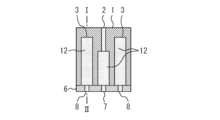
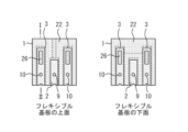
- FIG. 3A and 3B are diagrams showing upper and lower surfaces of a flexible substrate and an upper surface of a printed circuit board according to Embodiment 1;
- FIG. 1 is a top view showing a substrate bonding structure according to Embodiment 1;
- FIG. 3 is a cross-sectional view along I-II of FIG. 2;
- FIG. 1 is a circuit diagram showing an optical semiconductor device according to Embodiment 1;
- FIG. FIG. 4 is a cross-sectional view showing a connection structure between a package of an optical semiconductor device using a flexible substrate and a drive circuit; 4 is a circuit diagram showing a modification of the optical semiconductor device including the substrate bonding structure according to Embodiment 1;
- FIG. 4 is a circuit diagram showing a modification of the optical semiconductor device including the substrate bonding structure according to Embodiment 1;
- FIG. 4 is a circuit diagram showing a modification of the optical semiconductor device including the substrate bonding structure according to Embodiment 1;
- FIG. It is a figure which shows the upper-lower surface of a flexible substrate, and the upper surface of a printed circuit board which concerns on a comparative example.
- FIG. 10 is a diagram showing upper and lower surfaces of a flexible substrate according to Embodiment 2;
- FIG. 4 is a diagram showing the lower surface of a flexible substrate that is soldered without providing a solder resist; It is a figure which shows the lower surface of the flexible substrate which provided the soldering resist and joined by soldering.
- FIG. 10 is a diagram showing upper and lower surfaces of a flexible substrate according to Embodiment 2;
- FIG. 4 is a diagram showing the lower surface of a flexible substrate that is soldered without providing a solder resist; It is a figure which
- FIG. 10 is a diagram showing upper and lower surfaces of a flexible substrate and an upper surface of a printed circuit board according to Embodiment 3;
- FIG. 11 is a top view showing a substrate bonding structure according to Embodiment 3;
- FIG. 15 is a cross-sectional view along I-II of FIG. 14;
- FIG. 10 is a diagram showing the upper surface of the flexible substrate according to the third embodiment and the upper surfaces of modified examples 1 and 2 of the printed circuit board;
- FIG. 11 is a diagram showing upper and lower surfaces of a flexible substrate and an upper surface of a printed circuit board according to Embodiment 4;
- FIG. 11 is a top view showing a substrate bonding structure according to a fourth embodiment;
- FIG. 19 is a cross-sectional view along I-II of FIG.
- FIG. 11 is a diagram showing upper and lower surfaces of a flexible substrate according to Embodiment 5;
- FIG. 14 is a cross-sectional view showing a manufacturing process of a flexible substrate according to Embodiment 5;
- FIG. 14 is a cross-sectional view showing a manufacturing process of a flexible substrate according to Embodiment 5;
- a substrate bonding structure according to an embodiment will be described with reference to the drawings.
- the same reference numerals are given to the same or corresponding components, and repetition of description may be omitted.
- FIG. 1 is a diagram showing upper and lower surfaces of a flexible substrate and an upper surface of a printed circuit board according to Embodiment 1.
- FIG. A conductive pattern 2 and a GND pattern 3 are arranged parallel to each other on the top surface of a flexible substrate 1 .
- a conductive pattern 4 and a GND pattern 5 are arranged parallel to each other on the lower surface of the flexible substrate 1 .
- a conductive pattern 7 and a GND pattern 8 are arranged parallel to each other on the upper surface of the printed circuit board 6 .
- the conductive patterns 2, 4, 7 and the GND patterns 3, 5, 8 are made of copper foil, the surface of which is plated with gold.
- a through hole 9 is provided to penetrate the flexible substrate 1 and connect the conductive patterns 2 and 4.
- a through-hole 10 and a rectangular through-hole 11 are provided to pass through the flexible substrate 1 and connect the GND patterns 3 and 5 .
- the through hole 11 may be elliptical or rhombic.
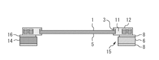
- FIG. 2 is a top view showing the substrate bonding structure according to Embodiment 1.
- FIG. FIG. 3 is a cross-sectional view along I-II of FIG.
- the substrate bonding structure is obtained by soldering the flexible substrate 1 and the printed substrate 6 together.
- the solder 12 joins the aligned conductive pattern 4 of the flexible substrate 1 and the conductive pattern 7 of the printed circuit board 6 and joins the GND pattern 5 and the GND pattern 8 .
- the tip of the flexible substrate 1 is aligned with the position of the dotted line A in FIG.
- the through hole 9 is filled with solder 12 to electrically connect the conductive pattern 2 on the top side and the conductive pattern 4 on the bottom side.
- the through holes 10 and 11 are filled with solder 12 to electrically connect the GND pattern 3 on the upper surface side of the flexible substrate 1 and the GND pattern 5 on the lower surface side.
- the side surfaces of the through holes 9, 10 and 11 are metallized in order to improve the wetting and spreading properties of the solder 12, the metallization may be omitted.
- the end of the solder joint between the conductive pattern 4 and the conductive pattern 7 is located at a position corresponding to the through hole 11 and deviated from the end of the through hole 11 ( See dashed line B in FIG. 1).
- the end of the solder joint is positioned at the center of the long side of through-hole 11 .
- the center position of the long side of the through-hole 11 may be set at the end of the printed circuit board 6 or the end of the conductive pattern 7, for example.
- FIG. 4 is a circuit diagram showing the optical semiconductor device according to Embodiment 1.
- FIG. A package 14 of the optical semiconductor device 13 and a drive circuit 15 are connected via the flexible substrate 1 .
- the optical semiconductor device 13 is a TOSA (Transmitter Optical Sub-Assembly).
- a light emitting element LD In the optical semiconductor device 13, a light emitting element LD, a terminating resistor R1, a capacitor C1 and a resistor R2 are arranged inside the package .
- the light emitting element LD is, for example, an EML-LD (Electro-Absorption Modulator Laser Diode).
- a light emitting element LD is connected in parallel with the resistor R2.
- a capacitor C1 and a terminating resistor R1 are connected in series with each other and in parallel with the light emitting element LD and the resistor R2.
- the anode of the light emitting element LD is connected to the drive circuit 15, and the cathode is connected to GND.
- the light emitting element LD emits light according to the high frequency modulated electric signal supplied from the drive circuit 15 .
- the terminating resistor R1 and the capacitor C1 may be arranged in this order from the drive circuit 15 side.
- FIG. 5 is a cross-sectional view showing a connection structure between a package of an optical semiconductor device using a flexible substrate and a drive circuit.
- the substrate bonding structure of this embodiment is applied to the connection between one end of the flexible substrate 1 and the drive circuit 15 .
- the substrate bonding structure of this embodiment may be applied to the connection between the other end of the flexible substrate 1 and the pattern 16 of the package 14 .
- 6 to 8 are circuit diagrams showing modifications of the optical semiconductor device including the substrate bonding structure according to the first embodiment. 6 shows the case without the resistor R2, and FIG. 7 shows the case without the resistor R2 and the capacitor C1.
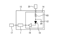
- the optical semiconductor device 13 in FIG. 8 is a ROSA (Receiver Optical Sub-Assembly).
- the package 14 of the optical semiconductor device 13 and the signal circuit 17 are connected by the flexible substrate 1 .
- a light receiving element 18, a capacitor C2, a resistor R3, and a transimpedance amplifier 19 are arranged inside the package .
- the light receiving element 18 is, for example, an APD (Avalanche Photo Diode).
- the anode of the light receiving element 18 is connected to the feeding circuit 20 through the resistor R3, and the cathode is connected to the input of the transimpedance amplifier 19.
- the output of the transimpedance amplifier 19 is connected to the signal circuit 17 via the flexible substrate 1 .
- the capacitor C is connected in parallel with the light receiving element 18 . Also, any or all of the capacitor C2, the resistor R3, and the transimpedance amplifier 19 may be omitted.
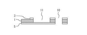
- FIG. 9 is a diagram showing upper and lower surfaces of a flexible substrate and an upper surface of a printed circuit board according to a comparative example.
- the coverlay film 21 covering the conductive pattern 2 on the upper surface of the flexible substrate 1 is provided with a convex portion, and the end of the solder joint is shifted from the bend of the flexible substrate 1.
- the manufacturing tolerance of the coverlay film 21 includes not only the lamination tolerance but also the overflow of the adhesive. Therefore, the manufacturing tolerance of the cover lay film 21 is as large as about ⁇ 400 ⁇ m. For this reason, the ends of the soldered joints are not sufficiently displaced from the bends of the flexible substrate 1, and the conductive pattern 2 on the front surface or the GND pattern 5 on the back surface may break.
- a through hole 11 that penetrates the flexible substrate 1 and connects the GND patterns 3 and 5 is provided. Since the through hole 11 is formed by drilling or laser processing, the manufacturing tolerance of the through hole 11 is as small as ⁇ 50 to 100 ⁇ m.
- the through holes 11 are filled with the solder 12. ⁇ In the direction in which the conductive pattern 4 extends, the end of the solder joint between the conductive pattern 4 and the conductive pattern 7 is located at a position corresponding to the through hole 11 and shifted from the end of the through hole 11 .
- the stress concentration point becomes the end of the through hole 11 (see dotted line C in FIG. 3), and stress is no longer applied to the end of the solder joint, thereby preventing disconnection. .
- Embodiment 2. 10A and 10B are diagrams showing upper and lower surfaces of a flexible substrate according to Embodiment 2.
- FIG. A solder resist 22 is provided on the upper and lower surfaces of the flexible substrate 1 where the solder 12 is not desired to be applied.
- the solder resist 22 is PSR-4000 G24K/CA-40 G24 manufactured by Taiyo Ink Mfg. Co., Ltd., for example.
- FIG. 11 is a diagram showing the bottom surface of a flexible substrate soldered without providing a solder resist.
- the solder 12 is widely wetted and spread on the GND pattern 5 .
- the GND pattern 5 will be disconnected due to the disconnection portion 23 occurring at the solder boundary.
- FIG. 12 is a diagram showing the bottom surface of a flexible substrate soldered with a solder resist.
- the solder resist 22 By providing the solder resist 22, when the flexible substrate 1 and the printed circuit board 6 are joined by soldering, the location where the solder 12 spreads can be controlled. Even if the solder 12 wets and spreads on the GND pattern 5, the solder resist 22 prevents the wet spreading. When a stress is applied to the flexible substrate 1, there is a possibility that a disconnection portion 23 may occur at the end of the solder joint, but the GND pattern 5 is not disconnected. Therefore, it can be used without affecting the characteristics.
- the solder resist 22 may be a coverlay film. Other configurations and effects are the same as those of the first embodiment.
- Embodiment 3. 13A and 13B are diagrams showing upper and lower surfaces of a flexible substrate and an upper surface of a printed circuit board according to Embodiment 3.
- FIG. A castellation 24 is provided on the side surface of the printed circuit board 6 at the tip of the GND pattern 8 .
- the castellation 24 is obtained by cutting out a part of the side surface of the substrate and metallizing it.
- the concave portion of the castellation 24 is aligned with the center of the long side of the through hole 11 as indicated by the dotted line B in FIG. Note that the solder resist 22 may be omitted.
- FIG. 14 is a top view showing a substrate bonding structure according to Embodiment 3.
- FIG. 15 is a cross-sectional view along I-II of FIG. 14.
- FIG. 14 When the flexible substrate 1 and the printed circuit board 6 are joined with the solder 12, the solder 12 spreads over the castellations 24 and solder bridges 25 are formed. Due to the solder 12 and the solder bridges 25 filled in the through holes 11 of the flexible substrate 1, the solder joints of the flexible substrate 1 are less likely to bend. As a result, the stress applied to the solder joint can be reduced, and disconnection can be prevented. In addition, since there is no need to reinforce with resin to prevent disconnection, manufacturing is facilitated.
- FIG. 16 is a diagram showing the upper surface of the flexible substrate according to the third embodiment and the upper surfaces of modified examples 1 and 2 of the printed circuit board.
- the concave portion of the castellation 24 is offset from the center of the long side of the through hole 11 . Similar effects can be obtained in this case as well.
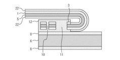
- Embodiment 4. 17A and 17B are diagrams showing upper and lower surfaces of a flexible substrate and an upper surface of a printed circuit board according to Embodiment 4.
- FIG. FIG. 18 is a top view showing the substrate bonding structure according to the fourth embodiment. 19 is a cross-sectional view along I-II of FIG. 18.
- FIG. A flexible substrate 1 extending from a solder joint is bent 180 degrees to the opposite side.
- the stress applied after bonding with the solder 12 can be dispersed. As a result, the stress on the solder joint can be reduced to prevent disconnection. Also, if the bonding strength between the flexible substrate 1 and the printed circuit board 6 is weak, the solder 12 will peel off and disconnection will occur when stress is applied. can be further prevented.
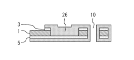
- Embodiment 5 20A and 20B are diagrams showing upper and lower surfaces of a flexible substrate according to Embodiment 5.
- FIG. Through hole 11 is filled with metal 26 .
- the metal 26 is a metal harder than the solder 12, such as copper. When stress is applied to the flexible substrate 1, the flexible substrate 1 is less likely to bend than when the through-holes 11 are filled with the solder 12, so disconnection can be further prevented.
- 21 and 22 are cross-sectional views showing manufacturing steps of the flexible substrate according to the fifth embodiment. 21 and 22 correspond to the section along I-II of FIG.
- through holes 11 are formed by removing a portion of the flexible substrate 1 and the GND pattern 3 on the surface side. At this time, the GND pattern 5 on the back side is not removed (blind via structure).
- the through holes 11 are filled with a metal 26 by copper plating.
- Other configurations and effects are the same as those of the first embodiment.
Landscapes
- Engineering & Computer Science (AREA)
- Microelectronics & Electronic Packaging (AREA)
- Manufacturing & Machinery (AREA)
- Combinations Of Printed Boards (AREA)
- Structure Of Printed Boards (AREA)
- Printing Elements For Providing Electric Connections Between Printed Circuits (AREA)
Priority Applications (7)
| Application Number | Priority Date | Filing Date | Title |
|---|---|---|---|
| JP2022523323A JP7180816B1 (ja) | 2021-12-20 | 2021-12-20 | 基板接合構造 |
| DE112021008535.2T DE112021008535T5 (de) | 2021-12-20 | 2021-12-20 | Substratverbindungsanordnung |
| CN202180100692.5A CN118355736A (zh) | 2021-12-20 | 2021-12-20 | 基板接合构造 |
| KR1020247007007A KR102893924B1 (ko) | 2021-12-20 | 2021-12-20 | 기판 접합 구조 |
| US18/576,236 US12507351B2 (en) | 2021-12-20 | 2021-12-20 | Substrate joining structure |
| PCT/JP2021/047007 WO2023119357A1 (ja) | 2021-12-20 | 2021-12-20 | 基板接合構造 |
| TW111143340A TWI841051B (zh) | 2021-12-20 | 2022-11-14 | 基板接合構造 |
Applications Claiming Priority (1)
| Application Number | Priority Date | Filing Date | Title |
|---|---|---|---|
| PCT/JP2021/047007 WO2023119357A1 (ja) | 2021-12-20 | 2021-12-20 | 基板接合構造 |
Publications (1)
| Publication Number | Publication Date |
|---|---|
| WO2023119357A1 true WO2023119357A1 (ja) | 2023-06-29 |
Family
ID=84271365
Family Applications (1)
| Application Number | Title | Priority Date | Filing Date |
|---|---|---|---|
| PCT/JP2021/047007 Ceased WO2023119357A1 (ja) | 2021-12-20 | 2021-12-20 | 基板接合構造 |
Country Status (7)
| Country | Link |
|---|---|
| US (1) | US12507351B2 (https=) |
| JP (1) | JP7180816B1 (https=) |
| KR (1) | KR102893924B1 (https=) |
| CN (1) | CN118355736A (https=) |
| DE (1) | DE112021008535T5 (https=) |
| TW (1) | TWI841051B (https=) |
| WO (1) | WO2023119357A1 (https=) |
Citations (5)
| Publication number | Priority date | Publication date | Assignee | Title |
|---|---|---|---|---|
| JPS5941894A (ja) * | 1982-09-01 | 1984-03-08 | ソニー株式会社 | フレキシブルプリント基板の半田付け装置 |
| JP2012105104A (ja) * | 2010-11-10 | 2012-05-31 | Fujitsu Optical Components Ltd | 光送信器及び中継基板 |
| WO2016203774A1 (ja) * | 2015-06-19 | 2016-12-22 | 日本電信電話株式会社 | フレキシブルプリント配線板のはんだ接合構造 |
| JP2017003655A (ja) * | 2015-06-05 | 2017-01-05 | 富士通オプティカルコンポーネンツ株式会社 | 光モジュール及び光送受信装置 |
| WO2019043933A1 (ja) * | 2017-09-04 | 2019-03-07 | 三菱電機株式会社 | フレキシブル基板および光モジュール |
Family Cites Families (5)
| Publication number | Priority date | Publication date | Assignee | Title |
|---|---|---|---|---|
| JP3623051B2 (ja) | 1996-08-26 | 2005-02-23 | ホシデン株式会社 | フレキシブル基板の半田付け接続構造 |
| KR100905404B1 (ko) * | 2006-08-07 | 2009-06-30 | 닛뽕 아비오닉스 가부시끼가이샤 | 프린트 배선판의 접속 방법 및 접속 장치 |
| JP5011531B2 (ja) | 2007-01-17 | 2012-08-29 | 国立大学法人長岡技術科学大学 | 深絞り加工装置 |
| CN109804720A (zh) * | 2016-12-28 | 2019-05-24 | 株式会社藤仓 | 布线体组件、布线基板以及接触式传感器 |
| CN115475268B (zh) * | 2021-05-30 | 2024-11-12 | 宝洁公司 | 清新组合物 |
-
2021
- 2021-12-20 KR KR1020247007007A patent/KR102893924B1/ko active Active
- 2021-12-20 DE DE112021008535.2T patent/DE112021008535T5/de not_active Withdrawn
- 2021-12-20 JP JP2022523323A patent/JP7180816B1/ja active Active
- 2021-12-20 US US18/576,236 patent/US12507351B2/en active Active
- 2021-12-20 CN CN202180100692.5A patent/CN118355736A/zh active Pending
- 2021-12-20 WO PCT/JP2021/047007 patent/WO2023119357A1/ja not_active Ceased
-
2022
- 2022-11-14 TW TW111143340A patent/TWI841051B/zh active
Patent Citations (5)
| Publication number | Priority date | Publication date | Assignee | Title |
|---|---|---|---|---|
| JPS5941894A (ja) * | 1982-09-01 | 1984-03-08 | ソニー株式会社 | フレキシブルプリント基板の半田付け装置 |
| JP2012105104A (ja) * | 2010-11-10 | 2012-05-31 | Fujitsu Optical Components Ltd | 光送信器及び中継基板 |
| JP2017003655A (ja) * | 2015-06-05 | 2017-01-05 | 富士通オプティカルコンポーネンツ株式会社 | 光モジュール及び光送受信装置 |
| WO2016203774A1 (ja) * | 2015-06-19 | 2016-12-22 | 日本電信電話株式会社 | フレキシブルプリント配線板のはんだ接合構造 |
| WO2019043933A1 (ja) * | 2017-09-04 | 2019-03-07 | 三菱電機株式会社 | フレキシブル基板および光モジュール |
Also Published As
| Publication number | Publication date |
|---|---|
| KR102893924B1 (ko) | 2025-12-01 |
| CN118355736A (zh) | 2024-07-16 |
| TW202327414A (zh) | 2023-07-01 |
| JPWO2023119357A1 (https=) | 2023-06-29 |
| JP7180816B1 (ja) | 2022-11-30 |
| US20240314943A1 (en) | 2024-09-19 |
| KR20240042003A (ko) | 2024-04-01 |
| TWI841051B (zh) | 2024-05-01 |
| US12507351B2 (en) | 2025-12-23 |
| DE112021008535T5 (de) | 2024-10-10 |
Similar Documents
| Publication | Publication Date | Title |
|---|---|---|
| US7306377B2 (en) | Integrated optical sub-assembly having epoxy chip package | |
| JP4685614B2 (ja) | 基板及び基板モジュール | |
| JPWO2016129277A1 (ja) | フレキシブル基板及び光モジュール | |
| JP6570976B2 (ja) | 光モジュール | |
| JP5426730B2 (ja) | 光モジュール用パッケージ | |
| JP5706254B2 (ja) | 半導体装置 | |
| JP7180816B1 (ja) | 基板接合構造 | |
| JP2017058607A (ja) | 光伝送装置及び光モジュール | |
| CN112640094B (zh) | 光模块 | |
| CN110637399B (zh) | 光模块及其制造方法 | |
| JP4131724B2 (ja) | 回路基板への端子の取付構造 | |
| CN113614925A (zh) | 光模块 | |
| JP7265460B2 (ja) | 光モジュール | |
| KR20020092239A (ko) | 전자 부품들이 장착된 프린팅된 회로 기판을 포함하는구조체 및 이를 제조하기 위한 방법 | |
| JP6308870B2 (ja) | 光モジュール | |
| JP2024005971A (ja) | 半導体装置 | |
| JP2011222363A (ja) | 端子、電子回路部品 | |
| JP2005294407A (ja) | プリント基板およびその製造方法 | |
| JP6317226B2 (ja) | フレキシブルプリント基板搭載パッケージおよびその製造方法 | |
| JP7158436B2 (ja) | 回路素子、回路素子の製造方法、及び電気信号伝送方法 | |
| JP2019153674A (ja) | 光モジュール | |
| JP2008263055A (ja) | 電子部品実装体 | |
| CN104101961A (zh) | 光学通讯装置 | |
| JP2006156682A (ja) | モジュール | |
| JP2016164925A (ja) | 光モジュール |
Legal Events
| Date | Code | Title | Description |
|---|---|---|---|
| WWE | Wipo information: entry into national phase |
Ref document number: 2022523323 Country of ref document: JP |
|
| 121 | Ep: the epo has been informed by wipo that ep was designated in this application |
Ref document number: 21968795 Country of ref document: EP Kind code of ref document: A1 |
|
| WWE | Wipo information: entry into national phase |
Ref document number: 202180100692.5 Country of ref document: CN |
|
| WWE | Wipo information: entry into national phase |
Ref document number: 112021008535 Country of ref document: DE |
|
| 122 | Ep: pct application non-entry in european phase |
Ref document number: 21968795 Country of ref document: EP Kind code of ref document: A1 |