WO2023112962A1 - 水晶振動素子及び水晶デバイス - Google Patents
水晶振動素子及び水晶デバイス Download PDFInfo
- Publication number
- WO2023112962A1 WO2023112962A1 PCT/JP2022/046045 JP2022046045W WO2023112962A1 WO 2023112962 A1 WO2023112962 A1 WO 2023112962A1 JP 2022046045 W JP2022046045 W JP 2022046045W WO 2023112962 A1 WO2023112962 A1 WO 2023112962A1
- Authority
- WO
- WIPO (PCT)
- Prior art keywords
- crystal
- electrode
- electrodes
- excitation
- mounting
- Prior art date
- Legal status (The legal status is an assumption and is not a legal conclusion. Google has not performed a legal analysis and makes no representation as to the accuracy of the status listed.)
- Ceased
Links
Images



Classifications
-
- H—ELECTRICITY
- H03—ELECTRONIC CIRCUITRY
- H03H—IMPEDANCE NETWORKS, e.g. RESONANT CIRCUITS; RESONATORS
- H03H9/00—Networks comprising electromechanical or electro-acoustic elements; Electromechanical resonators
- H03H9/15—Constructional features of resonators consisting of piezoelectric or electrostrictive material
- H03H9/17—Constructional features of resonators consisting of piezoelectric or electrostrictive material having a single resonator
- H03H9/19—Constructional features of resonators consisting of piezoelectric or electrostrictive material having a single resonator consisting of quartz
Definitions
- the present disclosure relates to crystal oscillators and crystal devices.
- a crystal resonator element that resonates a crystal blank to output a signal of a desired frequency
- the quality of vibration deteriorates when the vibration reaches the edge of the crystal blank.
- An excitation electrode is located across which a voltage associated with resonance is applied. When the resonance frequency becomes high, the plane view size of the excitation electrode can be made smaller than that of the crystal piece.
- Japanese Patent Application Laid-Open No. 2017-050751 discloses that the extraction direction of extraction electrodes that connect the excitation electrodes and the mounting electrodes for external connection is set with respect to the X-axis (electrical axis) direction related to the vibration of the crystal piece.
- Equivalent Serial Resistance (ESR) or Crystal Impedance (CI) is suppressed from increasing by setting an appropriate angle.
- One aspect of the present disclosure is a crystal piece having a resonance frequency of 100 MHz or higher; two excitation electrodes to which a voltage related to resonance of the crystal piece is applied; two mounting electrodes located close to one end of the crystal piece and connected to the outside; two extraction electrodes respectively connecting the excitation electrodes and the mounting electrodes; with the center of the excitation electrode is positioned closer to the mounting electrode than the center position of the crystal blank,
- the two extraction electrodes are crystal vibrating elements that connect the excitation electrodes and the mounting electrodes in non-parallel and straight lines.
- FIG. 2 is a perspective view showing the configuration of the crystal device of the present embodiment with the lid removed.
- 1 is a cross-sectional view of a quartz device;
- FIG. It is a top view in the state which removed the lid
- It is an experiment result which shows the temperature characteristic of ESR when an extraction electrode has a bend.
- It is an experiment result which shows the temperature characteristic of ESR when an extraction electrode does not bend.
- 5 is a graph showing experimental results of ESR depending on the width of the extraction electrode; 5 is a graph showing experimental results of ESR depending on the width of the extraction electrode; 5 is a graph showing experimental results of ESR depending on the width of the extraction electrode;
- FIG. 1A and 1B are diagrams showing the configuration of a crystal device 1 of this embodiment.
- 1A is a perspective view showing a state in which the lid body 14 is removed
- FIG. 1B is a cross-sectional view taken along the cross-sectional line AA in FIG. 1A.
- the crystal device 1 includes a base 11, a crystal vibrating element 12, a conductive adhesive 13, a lid 14, parts 15, and the like.
- the base 11 has a bottom plate 111 and side walls 112 positioned on the periphery of the upper surface of the bottom plate 111, and has a box-like shape with a recess 11a surrounded by the bottom plate 111 and the side walls 112.
- An electrode pad 113 is positioned on the bottom surface of the recess 11a.
- external connection pads 114 are located on the back surface (surface on the ⁇ z side) of the bottom plate 111 .
- a dotted line is shown between the bottom plate 111 and the side wall portion 112 for the sake of explanation, but they are actually integrated.
- the crystal vibrating element 12 is connected to the electrode pad 113 via the conductive adhesive 13 .
- the electrode pads 113 are electrically connected to external connection pads 114 via electrical wiring (not shown) located inside the base 11 . Note that the electrode pads 113 may be positioned on the projecting portion positioned on the upper surface of the bottom plate 111 .
- the external connection pads 114 are connected to the module board or the like using, for example, solder, so that the crystal device 1 can transmit and receive signals to and from the external module board and the like.
- the crystal vibrating element 12 has a crystal piece 121, an excitation electrode 122, an extraction electrode 123, a mounting electrode 124, and the like.
- the mounting electrode 124 is an electrode for mounting the crystal vibrating element 12 on the base 11, and near the end of the crystal piece 121 on the +x side, here, two (a pair of) mounting electrodes 1241 and 1242 are respectively mounted. They are positioned in contact with the ends on the +x side and are connected and fixed to the electrode pads 113 via the conductive adhesive 13 . Thereby, the excitation electrode 122 is connected to the outside through the electrode pad 113 and the external connection pad 114 . Thus, the crystal vibrating element 12 is in a cantilevered state.
- the excitation electrode 122 has two excitation electrodes 1221 on the lower surface side of the crystal piece 121 (the side facing the bottom plate 111, -z side) and an excitation electrode 1222 on the upper surface side (+z side). These two excitation electrodes 122 are located at the same position in plan view from the upper surface side.
- the excitation electrode 1221 is electrically connected to the mounting electrode 1241 via the extraction electrode 1231 .
- the excitation electrode 1222 is electrically connected to the mounting electrode 1242 via the extraction electrode 1232 .
- a mounting electrode 1242 connected to the extraction electrode 1232 located on the upper surface side spreads over both upper and lower surfaces.
- the external connection pad 114 and the excitation electrode 122 are connected to each other via the conductive adhesive 13 on the lower surface side of the crystal vibrating element 12, and a voltage for resonance is applied. That is, a voltage signal is applied to the excitation electrodes 122 to vibrate (excite) the crystal blank 121 , or a voltage generated between the excitation electrodes 122 is output to the external connection pads 114 .
- the crystal piece 121 is, for example, an AT-cut rectangular piece, and has a thickness corresponding to the resonance frequency to be output. Normally, the higher the resonance frequency, the thinner the crystal piece 121 becomes. Although not particularly limited, here, the crystal piece 121 has a resonance frequency of 100 MHz or higher. Note that the crystal piece 121 is not limited to having a uniform thickness as a whole.
- the portion of the mounting electrode 124 may be thicker than the thickness of the contact area with the excitation electrode 122 that causes vibration and the thickness of the surrounding area (these are referred to as a vibrating portion). It may have a relatively thick portion surrounding the vibrating portion. Alternatively, conversely, crystal piece 121 may have a shape in which the periphery is relatively thin compared to the vibrating portion.
- the direction (X-axis direction) along the crystal axis (electrical axis) of the crystal blank 121 coincides with the x-axis direction in the drawing, and the sides extending in the X-axis direction are the long sides of the rectangular shape (rectangle).
- a lid 14 is joined to the upper end surface of the side wall portion 112 surrounding the concave portion 11a of the base 11 with a brazing material or the like.
- a metallized layer (not shown), which is a frame-shaped conductor and has substantially the same shape as the side wall portion 112 in plan view, may be positioned.
- the metallized layer may be a conductive layer obtained by coating and firing, or may be a plated layer.
- the recessed portion 11a is sealed by the lid 14 to block entry and exit of air, dust, and the like with the outside.
- the base 11 and the lid 14 are a housing that accommodates the crystal vibrating element 12 in the crystal device 1 of this embodiment.
- the part 15 is positioned on the bottom side of the base 11 .
- the component 15 may be an electronic component such as an IC chip, or may be a sensor such as a temperature detecting element (thermistor, etc.). Also, the parts 15 may be of the same type or a combination of multiple types. These are for outputting supplementary information relating to adjustment of the resonance frequency of the crystal oscillator 12, or performing adjustment according to the supplementary information. That is, the crystal device 1 may be a crystal oscillator. . Note that the position of the component 15 may not be near the center of the bottom surface in plan view, but may be at a deviated position.
- the substrate 11 is not particularly limited, but may be, for example, a ceramic material, a semiconductor material, a glass material, or a crystal, or a combination thereof. (including things).
- the conductive electrode pads 113 may be printed on the substrate 11, for example, and the uppermost surface thereof may be plated with gold, for example.
- the conductive adhesive 13 may be, for example, a resin-based (silicone-based resin, epoxy resin, or the like) adhesive containing a silver filler.
- the conductive adhesive 13 made of silicone resin is soft even after being adhered, so it is less likely to adversely affect vibrations.
- the lid 14 is a metal conductor flat plate, for example, a metal containing iron, copper, nickel, chromium, cobalt, molybdenum or tungsten, or an alloy thereof.
- FIG. 2 is a plan view of the crystal device 1 of this embodiment with the cover 14 removed. A portion of the configuration that cannot be seen from the top side is indicated by a dashed line. A dotted line indicates the center of the crystal vibrating element 12 in the x-axis direction (direction along the long side).
- the excitation electrode 122 of the crystal vibrating element 12 is here circular. Further, the center position of the excitation electrode 122 is closer to the mounting electrode 124 side than the center position of the crystal vibrating element 12 .
- the excitation electrode 122 has an area approximately equal to or slightly smaller than that of the vibrating portion of the crystal piece 121 at a resonance frequency of 100 MHz or more. If this area is close to the area of the crystal piece 121, the vibration characteristics are degraded due to the influence of the edge of the crystal piece 121. FIG.
- the vibration characteristics are also affected by the angle of the excitation electrode 122 . Here, by rounding the corners of the excitation electrode 122 to make it particularly circular in plan view, the adverse effect on the vibration characteristics is reduced.
- the length of the crystal blank 121 in the x-axis direction (that is, the X-axis direction) can be shortened accordingly, but it does not necessarily have to be shortened.
- the length of the side (long side) of the crystal piece 121 in the x-axis direction can be in the range of 0.8 to 1.4 mm, for example.
- the length of the side (short side) of the crystal blank 121 in the y-axis direction can be in the range of 0.4 to 1.0 mm, for example.
- the extraction electrodes 1231 and 1232 (summarization) , the two lead-out electrodes 123) become longer. Since the lead-out electrode 123 is thinner than the excitation electrode 122, the mounting electrode 124, etc., if it becomes longer, it leads to an increase in ESR (CI). As described above, in the crystal vibrating element 12 having a resonance frequency of 100 MHz or more, the vibration does not spread outside the range of the excitation electrodes 122.
- the extraction electrodes 123 are not advantageous in separating the excitation electrodes 122 from the mounting electrodes 124 and the like.
- the disadvantage of being longer is greater. Therefore, in this crystal vibrating element 12 , the center position of the excitation electrode 122 in plan view is closer to the mounting electrode 124 than the center position of the crystal piece 121 in plan view.
- the length M1 (distance) between the center position of the excitation electrode 122 and the center position of the crystal piece 121 in plan view is usually greater than 0 ⁇ m and less than 550 ⁇ m, preferably greater than 0 ⁇ m and less than or equal to 540 ⁇ m. , particularly preferably larger than 0 ⁇ m and 440 ⁇ m or less.
- the ratio of the length M1 to the length of the side (long side) of the crystal piece 121 in the x-axis direction is usually 0.393 or less, preferably 0.386 or less, and particularly preferably 0.315 or less. be. If the excitation electrode 122 is too small, the voltage amplitude required to obtain the necessary vibration will be large, resulting in poor efficiency.
- the inner diameter (diameter) of the excitation electrode 122 is usually 150 ⁇ m or more and 900 ⁇ m or less, preferably 160 ⁇ m or more and 600 ⁇ m or less, and particularly preferably 170 ⁇ m or more and 400 ⁇ m or less.
- the area ratio of the excitation electrode 122 to the vibrating portion of the crystal element 121 in plan view is usually 0.005 or more and 0.785 or less, preferably 0.060 or more and 0.500 or less, and particularly preferably 0.060 or more and 0.500 or less. 070 or more and 0.130 or less.
- the two lead-out electrodes 123 are non-parallel to each other, and are straight lines extending in a direction inclined with respect to the side E1 of the rectangular mounting electrode 124 on the excitation electrode 122 side. . Since the lead-out electrode 123 does not have a bent portion, it is possible to shorten the connection points between the mounting electrodes 124 and the excitation electrodes 122 .
- the ratio of the side E1 to the short side of the crystal piece 121 is usually 0.10 or more and less than 0.50, preferably 0.18 or more and 0.50. 0.45 or less, and particularly preferably 0.20 or more and 0.40 or less.
- the length of the lead-out electrode 123 is appropriately adjusted when the direction radially extending from the center of curvature is closer to the direction perpendicular to the side E1 than the direction perpendicular to the side E1.
- the lead-out electrode 123 does not extend in the direction perpendicular to the side E1, ie, in the x-direction, the influence on the vibration of the crystal piece 121 can be reduced. If the lead-out electrode 123 is not parallel to the x-direction, the magnitude of the inclination angle ⁇ has little effect on the improvement of the ESR.
- the angle ⁇ is, for example, about 115 to 130 degrees.
- the width W of the lead-out electrode 123 perpendicular to the extending direction varies from the width L1 at the connection position from the connection position with the excitation electrode 122 to the width L2 toward the connection position with the mounting electrode 124. and may be gradually increased. Simply put, the thicker the lead-out electrode 123 is, the more the increase in ESR (CI) can be suppressed. Therefore, ideally, the ESR does not decrease. Further, in high-frequency band signal transmission, if there is a sudden (discontinuous) width change in the middle of the wiring, a characteristic impedance mismatch will occur, and the wiring resistance will tend to increase. It can also lead to spurious emissions and deterioration of fitting.
- the width L1 at the connection position with the excitation electrode 122 is shorter than the side E1.
- it is usually 30 ⁇ m or more and 180 ⁇ m or less, preferably 35 ⁇ m or more and 150 ⁇ m or less, and particularly preferably 40 ⁇ m or more and 120 ⁇ m or less.
- the ratio of the width L1 to the side E1 is usually 0.15 or more and less than 1, preferably 0.2 or more and 0.9 or less, and particularly preferably 0.3 or more and 0.8 or less.
- Width L2 at the connection position with mounting electrode 124 is not particularly limited as long as it is longer than width L1 and equal to or less than side E1. It is preferably 40 ⁇ m or more and 120 ⁇ m or less.
- the ratio of the width of the excitation electrode 122 to the side E1 is usually 0.03 or more and 0.50 or less, preferably , 0.10 or more and 0.45 or less, particularly preferably 0.20 or more and 0.40 or less.
- the ratio of width L1 to width L2 is usually 0.15 or more and less than 1, preferably 0.2 or more and 0.9 or less, and particularly preferably 0.3 or more and 0.8 or less. It is preferable that the ratio of the width L2 to the width L1 is within the above range, since spurious vibration is less likely to occur and wiring resistance is less likely to increase.
- 3A and 3B are experimental results showing temperature characteristics of ESR depending on whether or not the extraction electrode 123 is bent.
- the crystal piece 121 (long side 1166 ⁇ m, short side 787 ⁇ m) has a vibrating portion (long side 350 ⁇ m, short side 350 ⁇ m) corresponding to the circular excitation electrode 122 having a diameter of 330 ⁇ m.
- a length M1 between the center position and the center position of the crystal piece 121 in plan view is 170 ⁇ m.
- the distance from the mounting electrode 124 of the vibration electrode 122 is different, and the extraction electrode 123 with a width of 75 ⁇ m is connected to the same position of the excitation electrode 122 and the mounting electrode 124 (side E1: 180 ⁇ m).
- the angle between the direction of the extraction electrode 123 extending from the connection position with the excitation electrode 122 and the tangential line at the connection position with the mounting electrode 124 is 125 degrees.
- the distance is long, and the extraction electrode 123 is bent and connected perpendicularly to the side E1.
- the distance is short, and the extraction electrode 123 is connected directly obliquely to the side E1 without bending.
- the thickness of the electrode and extraction electrode is 210 nm each.
- the unbent lead-out electrode 123 directly and obliquely connects the side E1 of the mounting electrode 124 and the excitation electrode 122, thereby lowering the ESR, which is sufficiently below 20 ⁇ which is acceptable for product quality. I understand.
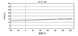
- FIGS. 4A to 4C are graphs showing experimental results of ESR in which the width W of the extraction electrode 123 was set as shown below in the crystal resonator element 12 used in FIG. 3B.
- 4A shows a shape in which the width W is 75 ⁇ m
- FIG. 4B shows a shape in which the width W gradually increases from 75 ⁇ m (L1) to 105 ⁇ m (L2)
- FIG. 4C shows a case in which the width W is 105 ⁇ m.
- the angle formed by the extraction electrode 123 with respect to the tangent to the connection position between the extraction electrode 123 and the mounting electrode 124 in FIG. 4B is in the range of 116 to 131 degrees.
- the ESR is significantly reduced compared to when the width W is constant at 75 ⁇ m. Also, compared with the case where the width W is constant at 105 ⁇ m, the ESR is lowered in the temperature range of about 0 to 100°C. As described above, it can be seen that the deterioration of the ESR of the crystal vibrating element 12 is effectively suppressed by widening the width W of the extraction electrode 123 while properly matching.
- the crystal vibrating element 12 of this embodiment includes a crystal blank 121 having a resonance frequency of 100 MHz or higher, two excitation electrodes 122 to which a voltage related to resonance of the crystal blank 121 is applied, and one end of the crystal blank 121. , two mounting electrodes 124 connected to the outside, and two extraction electrodes 123 connecting the excitation electrode 122 and the mounting electrode 124, respectively.
- the center of the excitation electrode 122 is positioned closer to the mounting electrode 124 than the center position of the crystal piece 121, and the two lead-out electrodes 123 are non-parallel and linear to each other between the excitation electrode 122 and the mounting electrode 124. connected.
- the extraction electrodes 123 can be efficiently shortened.
- the vibration does not largely protrude from the range of the excitation electrode 122. Therefore, even if the excitation electrode 122 and the mounting electrode 124 are brought close to each other with such a positional relationship, the mounting electrode does not respond to the vibration. Since the influence of 124 is suppressed to be small, it is possible to suppress the increase in ESR (CI) and to vibrate appropriately.
- the lead-out electrodes 123 are set in a non-parallel positional relationship, at least one of them (usually having the same shape and length) is tilted with respect to the vibration direction of the AT-cut crystal piece 121, so that the lead-out electrodes 123 can also reduce the influence on the vibration of In addition, since the extraction electrode 123 does not have a bent portion, it is possible to suppress signal reflection loss due to bending.
- the width of the extraction electrode 123 perpendicular to the extending direction from the excitation electrode 122 gradually increases from the connection position with the excitation electrode 122 toward the connection position with the mounting electrode 124 .
- an increase in ESR (CI) can be suppressed while matching impedance.
- the crystal resonator element 12 can appropriately suppress an increase in ESR (CI).
- the length of the long side (along the X-axis direction) of the crystal piece 121 is 1.4 mm or less. The above effect can be obtained remarkably when the size is appropriate for the crystal piece 121 of the crystal vibrating element 12 having a high resonance frequency of 100 MHz or more.
- the ratio of the length M1 between the center position of the excitation electrode 122 and the center position of the crystal blank 121 to the length of the long side of the crystal blank 121 is set to 0.393 or less. Such positioning effectively shortens the distance between the excitation electrode 122 and the mounting electrode 124 to shorten the length of the extraction electrode 123, thereby reducing the equivalent series resistance. Along with this, an increase in ESR (CI) can be suppressed, and the oscillation of the crystal blank 121 can be properly maintained.
- the crystal device 1 of the present embodiment includes the crystal oscillator 12 described above.
- accurate processing can be performed using a crystal oscillator 12 that operates more stably at an appropriate resonance frequency than before.
- excitation electrode 122 may not be perfectly circular.
- the excitation electrode 122 may be elliptical or square with rounded corners (rectangular, diamond-shaped, etc.) as desired. If the excitation electrode 122 is too small, the voltage amplitude required to obtain the necessary vibration will be large, which is inefficient.
- the size and shape of the crystal piece 121 may be appropriately adjusted according to the above conditions regarding the resonance frequency, the excitation electrode 122, and the like.
- the width of the lead-out electrode 123 need not be limited to that which simply gradually increases from the excitation electrode 122 toward the mounting electrode 124 .
- it may be adjusted as appropriate according to conditions such as spurious and fitting, and contents that are preferentially required for the crystal device 1 .
- crystal oscillator 12 may be sold or otherwise distributed separately from the substrate 11 or the like.
- specific configurations, structures, materials, and the like shown in the above embodiments can be changed as appropriate without departing from the gist of the present invention.
- the scope of the present invention includes the scope of the invention described in the claims and the scope of equivalents thereof.
- This invention can be used for crystal oscillators and crystal devices.
Landscapes
- Physics & Mathematics (AREA)
- Acoustics & Sound (AREA)
- Piezo-Electric Or Mechanical Vibrators, Or Delay Or Filter Circuits (AREA)
Priority Applications (1)
| Application Number | Priority Date | Filing Date | Title |
|---|---|---|---|
| JP2023567816A JPWO2023112962A1 (https=) | 2021-12-15 | 2022-12-14 |
Applications Claiming Priority (2)
| Application Number | Priority Date | Filing Date | Title |
|---|---|---|---|
| JP2021-202960 | 2021-12-15 | ||
| JP2021202960 | 2021-12-15 |
Publications (1)
| Publication Number | Publication Date |
|---|---|
| WO2023112962A1 true WO2023112962A1 (ja) | 2023-06-22 |
Family
ID=86774403
Family Applications (1)
| Application Number | Title | Priority Date | Filing Date |
|---|---|---|---|
| PCT/JP2022/046045 Ceased WO2023112962A1 (ja) | 2021-12-15 | 2022-12-14 | 水晶振動素子及び水晶デバイス |
Country Status (2)
| Country | Link |
|---|---|
| JP (1) | JPWO2023112962A1 (https=) |
| WO (1) | WO2023112962A1 (https=) |
Cited By (1)
| Publication number | Priority date | Publication date | Assignee | Title |
|---|---|---|---|---|
| WO2025205228A1 (ja) * | 2024-03-27 | 2025-10-02 | 京セラ株式会社 | 振動片、圧電振動素子、圧電振動子及び振動片の製造方法 |
Citations (4)
| Publication number | Priority date | Publication date | Assignee | Title |
|---|---|---|---|---|
| JPH077363A (ja) * | 1991-08-31 | 1995-01-10 | Nippon Dempa Kogyo Co Ltd | Scカットの水晶振動子 |
| JP2004214835A (ja) * | 2002-12-27 | 2004-07-29 | Nippon Dempa Kogyo Co Ltd | 多周波型水晶振動子 |
| JP2007208771A (ja) * | 2006-02-03 | 2007-08-16 | Epson Toyocom Corp | 圧電振動素子、圧電振動子及び圧電発振器 |
| WO2009020022A1 (ja) * | 2007-08-03 | 2009-02-12 | Daishinku Corporation | 圧電振動子 |
Family Cites Families (8)
| Publication number | Priority date | Publication date | Assignee | Title |
|---|---|---|---|---|
| JPH0640612B2 (ja) * | 1986-03-31 | 1994-05-25 | 朝日電波株式会社 | 圧電振動子 |
| JPH02226907A (ja) * | 1989-02-28 | 1990-09-10 | Nippon Dempa Kogyo Co Ltd | 水晶振動子 |
| JPH0472721U (https=) * | 1990-11-01 | 1992-06-26 | ||
| JPH0488113U (https=) * | 1990-12-12 | 1992-07-30 | ||
| JP4384329B2 (ja) * | 2000-03-31 | 2009-12-16 | 京セラ株式会社 | 圧電デバイス |
| JP4158700B2 (ja) * | 2003-12-26 | 2008-10-01 | 株式会社大真空 | 圧電振動片および圧電振動デバイス |
| JP2015109633A (ja) * | 2013-10-22 | 2015-06-11 | 株式会社大真空 | 圧電振動素子と当該圧電振動素子を用いた圧電デバイスおよび、前記圧電振動素子の製造方法と当該圧電振動素子を用いた圧電デバイスの製造方法 |
| JP6701161B2 (ja) * | 2015-02-18 | 2020-05-27 | 株式会社村田製作所 | 圧電振動デバイス及びその製造方法 |
-
2022
- 2022-12-14 JP JP2023567816A patent/JPWO2023112962A1/ja active Pending
- 2022-12-14 WO PCT/JP2022/046045 patent/WO2023112962A1/ja not_active Ceased
Patent Citations (4)
| Publication number | Priority date | Publication date | Assignee | Title |
|---|---|---|---|---|
| JPH077363A (ja) * | 1991-08-31 | 1995-01-10 | Nippon Dempa Kogyo Co Ltd | Scカットの水晶振動子 |
| JP2004214835A (ja) * | 2002-12-27 | 2004-07-29 | Nippon Dempa Kogyo Co Ltd | 多周波型水晶振動子 |
| JP2007208771A (ja) * | 2006-02-03 | 2007-08-16 | Epson Toyocom Corp | 圧電振動素子、圧電振動子及び圧電発振器 |
| WO2009020022A1 (ja) * | 2007-08-03 | 2009-02-12 | Daishinku Corporation | 圧電振動子 |
Cited By (1)
| Publication number | Priority date | Publication date | Assignee | Title |
|---|---|---|---|---|
| WO2025205228A1 (ja) * | 2024-03-27 | 2025-10-02 | 京セラ株式会社 | 振動片、圧電振動素子、圧電振動子及び振動片の製造方法 |
Also Published As
| Publication number | Publication date |
|---|---|
| JPWO2023112962A1 (https=) | 2023-06-22 |
Similar Documents
| Publication | Publication Date | Title |
|---|---|---|
| CN101340179B (zh) | 压电振动片及压电装置 | |
| US20110193642A1 (en) | Piezoelectric vibrator and oscillator using the same | |
| WO2023112962A1 (ja) | 水晶振動素子及び水晶デバイス | |
| JP4899519B2 (ja) | 表面実装型圧電発振器 | |
| JP4501875B2 (ja) | 圧電振動デバイスおよびその製造方法 | |
| CN101478297B (zh) | 用于表面安装的石英晶体器件 | |
| JP6569267B2 (ja) | 圧電発振器 | |
| JP7293037B2 (ja) | 水晶素子、水晶デバイス及び電子機器 | |
| JP7847263B2 (ja) | 水晶振動子 | |
| JP6690999B2 (ja) | 音叉型水晶片、音叉型水晶素子、水晶デバイスおよび音叉型水晶素子の製造方法 | |
| JP7660485B2 (ja) | 水晶デバイス及び電子機器 | |
| CN113875153B (zh) | 晶体元件以及晶体装置 | |
| CN1031739C (zh) | 振荡器 | |
| JP7645386B2 (ja) | 水晶振動素子及び水晶デバイス | |
| WO2025070156A1 (ja) | 圧電振動素子及び圧電振動子 | |
| JP2019220736A (ja) | 振動素子用の台座、振動子及び発振器 | |
| WO2025205708A1 (ja) | 圧電振動素子及び圧電デバイス | |
| JP2025163210A (ja) | 圧電共振デバイス | |
| JP2004356912A (ja) | 表面実装型圧電発振器 | |
| JP7145088B2 (ja) | 水晶デバイスの製造方法 | |
| TW202606204A (zh) | 壓電振動元件及壓電裝置 | |
| TW202606205A (zh) | 壓電振動元件及壓電裝置 | |
| WO2025197944A1 (ja) | 圧電振動素子及び圧電デバイス | |
| WO2025094647A1 (ja) | 圧電デバイス | |
| JP2018101920A (ja) | 水晶デバイス |
Legal Events
| Date | Code | Title | Description |
|---|---|---|---|
| 121 | Ep: the epo has been informed by wipo that ep was designated in this application |
Ref document number: 22907485 Country of ref document: EP Kind code of ref document: A1 |
|
| WWE | Wipo information: entry into national phase |
Ref document number: 2023567816 Country of ref document: JP |
|
| NENP | Non-entry into the national phase |
Ref country code: DE |
|
| 122 | Ep: pct application non-entry in european phase |
Ref document number: 22907485 Country of ref document: EP Kind code of ref document: A1 |