WO2023112962A1 - Crystal oscillator and crystal device - Google Patents
Crystal oscillator and crystal device Download PDFInfo
- Publication number
- WO2023112962A1 WO2023112962A1 PCT/JP2022/046045 JP2022046045W WO2023112962A1 WO 2023112962 A1 WO2023112962 A1 WO 2023112962A1 JP 2022046045 W JP2022046045 W JP 2022046045W WO 2023112962 A1 WO2023112962 A1 WO 2023112962A1
- Authority
- WO
- WIPO (PCT)
- Prior art keywords
- crystal
- electrode
- electrodes
- excitation
- mounting
- Prior art date
Links
- 239000013078 crystal Substances 0.000 title claims abstract description 125
- 230000005284 excitation Effects 0.000 claims abstract description 83
- 238000000605 extraction Methods 0.000 claims abstract description 39
- 239000000853 adhesive Substances 0.000 description 7
- 230000001070 adhesive effect Effects 0.000 description 7
- 239000000463 material Substances 0.000 description 4
- 238000005452 bending Methods 0.000 description 3
- 230000000694 effects Effects 0.000 description 3
- 238000002474 experimental method Methods 0.000 description 3
- 239000000758 substrate Substances 0.000 description 3
- XEEYBQQBJWHFJM-UHFFFAOYSA-N Iron Chemical compound [Fe] XEEYBQQBJWHFJM-UHFFFAOYSA-N 0.000 description 2
- PXHVJJICTQNCMI-UHFFFAOYSA-N Nickel Chemical compound [Ni] PXHVJJICTQNCMI-UHFFFAOYSA-N 0.000 description 2
- 230000002411 adverse Effects 0.000 description 2
- 239000004020 conductor Substances 0.000 description 2
- 230000006866 deterioration Effects 0.000 description 2
- 229910052751 metal Inorganic materials 0.000 description 2
- 239000002184 metal Substances 0.000 description 2
- 229920005989 resin Polymers 0.000 description 2
- 239000011347 resin Substances 0.000 description 2
- VYZAMTAEIAYCRO-UHFFFAOYSA-N Chromium Chemical compound [Cr] VYZAMTAEIAYCRO-UHFFFAOYSA-N 0.000 description 1
- RYGMFSIKBFXOCR-UHFFFAOYSA-N Copper Chemical compound [Cu] RYGMFSIKBFXOCR-UHFFFAOYSA-N 0.000 description 1
- ZOKXTWBITQBERF-UHFFFAOYSA-N Molybdenum Chemical compound [Mo] ZOKXTWBITQBERF-UHFFFAOYSA-N 0.000 description 1
- BQCADISMDOOEFD-UHFFFAOYSA-N Silver Chemical compound [Ag] BQCADISMDOOEFD-UHFFFAOYSA-N 0.000 description 1
- 239000000956 alloy Substances 0.000 description 1
- 229910045601 alloy Inorganic materials 0.000 description 1
- 238000005219 brazing Methods 0.000 description 1
- 229910010293 ceramic material Inorganic materials 0.000 description 1
- 229910052804 chromium Inorganic materials 0.000 description 1
- 239000011651 chromium Substances 0.000 description 1
- 239000011248 coating agent Substances 0.000 description 1
- 238000000576 coating method Methods 0.000 description 1
- 229910017052 cobalt Inorganic materials 0.000 description 1
- 239000010941 cobalt Substances 0.000 description 1
- GUTLYIVDDKVIGB-UHFFFAOYSA-N cobalt atom Chemical compound [Co] GUTLYIVDDKVIGB-UHFFFAOYSA-N 0.000 description 1
- 229910052802 copper Inorganic materials 0.000 description 1
- 239000010949 copper Substances 0.000 description 1
- 238000010586 diagram Methods 0.000 description 1
- 239000000428 dust Substances 0.000 description 1
- 238000009429 electrical wiring Methods 0.000 description 1
- 239000003822 epoxy resin Substances 0.000 description 1
- 239000000945 filler Substances 0.000 description 1
- 238000010304 firing Methods 0.000 description 1
- 239000011521 glass Substances 0.000 description 1
- PCHJSUWPFVWCPO-UHFFFAOYSA-N gold Chemical compound [Au] PCHJSUWPFVWCPO-UHFFFAOYSA-N 0.000 description 1
- 229910052737 gold Inorganic materials 0.000 description 1
- 239000010931 gold Substances 0.000 description 1
- 229910052742 iron Inorganic materials 0.000 description 1
- 238000012986 modification Methods 0.000 description 1
- 230000004048 modification Effects 0.000 description 1
- 229910052750 molybdenum Inorganic materials 0.000 description 1
- 239000011733 molybdenum Substances 0.000 description 1
- 229910052759 nickel Inorganic materials 0.000 description 1
- 230000010355 oscillation Effects 0.000 description 1
- 229920000647 polyepoxide Polymers 0.000 description 1
- 229920001296 polysiloxane Polymers 0.000 description 1
- 239000010453 quartz Substances 0.000 description 1
- 239000004065 semiconductor Substances 0.000 description 1
- 230000008054 signal transmission Effects 0.000 description 1
- VYPSYNLAJGMNEJ-UHFFFAOYSA-N silicon dioxide Inorganic materials O=[Si]=O VYPSYNLAJGMNEJ-UHFFFAOYSA-N 0.000 description 1
- 229920002050 silicone resin Polymers 0.000 description 1
- 229910052709 silver Inorganic materials 0.000 description 1
- 239000004332 silver Substances 0.000 description 1
- 229910000679 solder Inorganic materials 0.000 description 1
- WFKWXMTUELFFGS-UHFFFAOYSA-N tungsten Chemical compound [W] WFKWXMTUELFFGS-UHFFFAOYSA-N 0.000 description 1
- 229910052721 tungsten Inorganic materials 0.000 description 1
- 239000010937 tungsten Substances 0.000 description 1
Images


Classifications
-
- H—ELECTRICITY
- H03—ELECTRONIC CIRCUITRY
- H03H—IMPEDANCE NETWORKS, e.g. RESONANT CIRCUITS; RESONATORS
- H03H9/00—Networks comprising electromechanical or electro-acoustic devices; Electromechanical resonators
- H03H9/15—Constructional features of resonators consisting of piezoelectric or electrostrictive material
- H03H9/17—Constructional features of resonators consisting of piezoelectric or electrostrictive material having a single resonator
- H03H9/19—Constructional features of resonators consisting of piezoelectric or electrostrictive material having a single resonator consisting of quartz
Definitions
- the present disclosure relates to crystal oscillators and crystal devices.
- a crystal resonator element that resonates a crystal blank to output a signal of a desired frequency
- the quality of vibration deteriorates when the vibration reaches the edge of the crystal blank.
- An excitation electrode is located across which a voltage associated with resonance is applied. When the resonance frequency becomes high, the plane view size of the excitation electrode can be made smaller than that of the crystal piece.
- Japanese Patent Application Laid-Open No. 2017-050751 discloses that the extraction direction of extraction electrodes that connect the excitation electrodes and the mounting electrodes for external connection is set with respect to the X-axis (electrical axis) direction related to the vibration of the crystal piece.
- Equivalent Serial Resistance (ESR) or Crystal Impedance (CI) is suppressed from increasing by setting an appropriate angle.
- One aspect of the present disclosure is a crystal piece having a resonance frequency of 100 MHz or higher; two excitation electrodes to which a voltage related to resonance of the crystal piece is applied; two mounting electrodes located close to one end of the crystal piece and connected to the outside; two extraction electrodes respectively connecting the excitation electrodes and the mounting electrodes; with the center of the excitation electrode is positioned closer to the mounting electrode than the center position of the crystal blank,
- the two extraction electrodes are crystal vibrating elements that connect the excitation electrodes and the mounting electrodes in non-parallel and straight lines.
- FIG. 2 is a perspective view showing the configuration of the crystal device of the present embodiment with the lid removed.
- 1 is a cross-sectional view of a quartz device;
- FIG. It is a top view in the state which removed the lid
- It is an experiment result which shows the temperature characteristic of ESR when an extraction electrode has a bend.
- It is an experiment result which shows the temperature characteristic of ESR when an extraction electrode does not bend.
- 5 is a graph showing experimental results of ESR depending on the width of the extraction electrode; 5 is a graph showing experimental results of ESR depending on the width of the extraction electrode; 5 is a graph showing experimental results of ESR depending on the width of the extraction electrode;
- FIG. 1A and 1B are diagrams showing the configuration of a crystal device 1 of this embodiment.
- 1A is a perspective view showing a state in which the lid body 14 is removed
- FIG. 1B is a cross-sectional view taken along the cross-sectional line AA in FIG. 1A.
- the crystal device 1 includes a base 11, a crystal vibrating element 12, a conductive adhesive 13, a lid 14, parts 15, and the like.
- the base 11 has a bottom plate 111 and side walls 112 positioned on the periphery of the upper surface of the bottom plate 111, and has a box-like shape with a recess 11a surrounded by the bottom plate 111 and the side walls 112.
- An electrode pad 113 is positioned on the bottom surface of the recess 11a.
- external connection pads 114 are located on the back surface (surface on the ⁇ z side) of the bottom plate 111 .
- a dotted line is shown between the bottom plate 111 and the side wall portion 112 for the sake of explanation, but they are actually integrated.
- the crystal vibrating element 12 is connected to the electrode pad 113 via the conductive adhesive 13 .
- the electrode pads 113 are electrically connected to external connection pads 114 via electrical wiring (not shown) located inside the base 11 . Note that the electrode pads 113 may be positioned on the projecting portion positioned on the upper surface of the bottom plate 111 .
- the external connection pads 114 are connected to the module board or the like using, for example, solder, so that the crystal device 1 can transmit and receive signals to and from the external module board and the like.
- the crystal vibrating element 12 has a crystal piece 121, an excitation electrode 122, an extraction electrode 123, a mounting electrode 124, and the like.
- the mounting electrode 124 is an electrode for mounting the crystal vibrating element 12 on the base 11, and near the end of the crystal piece 121 on the +x side, here, two (a pair of) mounting electrodes 1241 and 1242 are respectively mounted. They are positioned in contact with the ends on the +x side and are connected and fixed to the electrode pads 113 via the conductive adhesive 13 . Thereby, the excitation electrode 122 is connected to the outside through the electrode pad 113 and the external connection pad 114 . Thus, the crystal vibrating element 12 is in a cantilevered state.
- the excitation electrode 122 has two excitation electrodes 1221 on the lower surface side of the crystal piece 121 (the side facing the bottom plate 111, -z side) and an excitation electrode 1222 on the upper surface side (+z side). These two excitation electrodes 122 are located at the same position in plan view from the upper surface side.
- the excitation electrode 1221 is electrically connected to the mounting electrode 1241 via the extraction electrode 1231 .
- the excitation electrode 1222 is electrically connected to the mounting electrode 1242 via the extraction electrode 1232 .
- a mounting electrode 1242 connected to the extraction electrode 1232 located on the upper surface side spreads over both upper and lower surfaces.
- the external connection pad 114 and the excitation electrode 122 are connected to each other via the conductive adhesive 13 on the lower surface side of the crystal vibrating element 12, and a voltage for resonance is applied. That is, a voltage signal is applied to the excitation electrodes 122 to vibrate (excite) the crystal blank 121 , or a voltage generated between the excitation electrodes 122 is output to the external connection pads 114 .
- the crystal piece 121 is, for example, an AT-cut rectangular piece, and has a thickness corresponding to the resonance frequency to be output. Normally, the higher the resonance frequency, the thinner the crystal piece 121 becomes. Although not particularly limited, here, the crystal piece 121 has a resonance frequency of 100 MHz or higher. Note that the crystal piece 121 is not limited to having a uniform thickness as a whole.
- the portion of the mounting electrode 124 may be thicker than the thickness of the contact area with the excitation electrode 122 that causes vibration and the thickness of the surrounding area (these are referred to as a vibrating portion). It may have a relatively thick portion surrounding the vibrating portion. Alternatively, conversely, crystal piece 121 may have a shape in which the periphery is relatively thin compared to the vibrating portion.
- the direction (X-axis direction) along the crystal axis (electrical axis) of the crystal blank 121 coincides with the x-axis direction in the drawing, and the sides extending in the X-axis direction are the long sides of the rectangular shape (rectangle).
- a lid 14 is joined to the upper end surface of the side wall portion 112 surrounding the concave portion 11a of the base 11 with a brazing material or the like.
- a metallized layer (not shown), which is a frame-shaped conductor and has substantially the same shape as the side wall portion 112 in plan view, may be positioned.
- the metallized layer may be a conductive layer obtained by coating and firing, or may be a plated layer.
- the recessed portion 11a is sealed by the lid 14 to block entry and exit of air, dust, and the like with the outside.
- the base 11 and the lid 14 are a housing that accommodates the crystal vibrating element 12 in the crystal device 1 of this embodiment.
- the part 15 is positioned on the bottom side of the base 11 .
- the component 15 may be an electronic component such as an IC chip, or may be a sensor such as a temperature detecting element (thermistor, etc.). Also, the parts 15 may be of the same type or a combination of multiple types. These are for outputting supplementary information relating to adjustment of the resonance frequency of the crystal oscillator 12, or performing adjustment according to the supplementary information. That is, the crystal device 1 may be a crystal oscillator. . Note that the position of the component 15 may not be near the center of the bottom surface in plan view, but may be at a deviated position.
- the substrate 11 is not particularly limited, but may be, for example, a ceramic material, a semiconductor material, a glass material, or a crystal, or a combination thereof. (including things).
- the conductive electrode pads 113 may be printed on the substrate 11, for example, and the uppermost surface thereof may be plated with gold, for example.
- the conductive adhesive 13 may be, for example, a resin-based (silicone-based resin, epoxy resin, or the like) adhesive containing a silver filler.
- the conductive adhesive 13 made of silicone resin is soft even after being adhered, so it is less likely to adversely affect vibrations.
- the lid 14 is a metal conductor flat plate, for example, a metal containing iron, copper, nickel, chromium, cobalt, molybdenum or tungsten, or an alloy thereof.
- FIG. 2 is a plan view of the crystal device 1 of this embodiment with the cover 14 removed. A portion of the configuration that cannot be seen from the top side is indicated by a dashed line. A dotted line indicates the center of the crystal vibrating element 12 in the x-axis direction (direction along the long side).
- the excitation electrode 122 of the crystal vibrating element 12 is here circular. Further, the center position of the excitation electrode 122 is closer to the mounting electrode 124 side than the center position of the crystal vibrating element 12 .
- the excitation electrode 122 has an area approximately equal to or slightly smaller than that of the vibrating portion of the crystal piece 121 at a resonance frequency of 100 MHz or more. If this area is close to the area of the crystal piece 121, the vibration characteristics are degraded due to the influence of the edge of the crystal piece 121. FIG.
- the vibration characteristics are also affected by the angle of the excitation electrode 122 . Here, by rounding the corners of the excitation electrode 122 to make it particularly circular in plan view, the adverse effect on the vibration characteristics is reduced.
- the length of the crystal blank 121 in the x-axis direction (that is, the X-axis direction) can be shortened accordingly, but it does not necessarily have to be shortened.
- the length of the side (long side) of the crystal piece 121 in the x-axis direction can be in the range of 0.8 to 1.4 mm, for example.
- the length of the side (short side) of the crystal blank 121 in the y-axis direction can be in the range of 0.4 to 1.0 mm, for example.
- the extraction electrodes 1231 and 1232 (summarization) , the two lead-out electrodes 123) become longer. Since the lead-out electrode 123 is thinner than the excitation electrode 122, the mounting electrode 124, etc., if it becomes longer, it leads to an increase in ESR (CI). As described above, in the crystal vibrating element 12 having a resonance frequency of 100 MHz or more, the vibration does not spread outside the range of the excitation electrodes 122.
- the extraction electrodes 123 are not advantageous in separating the excitation electrodes 122 from the mounting electrodes 124 and the like.
- the disadvantage of being longer is greater. Therefore, in this crystal vibrating element 12 , the center position of the excitation electrode 122 in plan view is closer to the mounting electrode 124 than the center position of the crystal piece 121 in plan view.
- the length M1 (distance) between the center position of the excitation electrode 122 and the center position of the crystal piece 121 in plan view is usually greater than 0 ⁇ m and less than 550 ⁇ m, preferably greater than 0 ⁇ m and less than or equal to 540 ⁇ m. , particularly preferably larger than 0 ⁇ m and 440 ⁇ m or less.
- the ratio of the length M1 to the length of the side (long side) of the crystal piece 121 in the x-axis direction is usually 0.393 or less, preferably 0.386 or less, and particularly preferably 0.315 or less. be. If the excitation electrode 122 is too small, the voltage amplitude required to obtain the necessary vibration will be large, resulting in poor efficiency.
- the inner diameter (diameter) of the excitation electrode 122 is usually 150 ⁇ m or more and 900 ⁇ m or less, preferably 160 ⁇ m or more and 600 ⁇ m or less, and particularly preferably 170 ⁇ m or more and 400 ⁇ m or less.
- the area ratio of the excitation electrode 122 to the vibrating portion of the crystal element 121 in plan view is usually 0.005 or more and 0.785 or less, preferably 0.060 or more and 0.500 or less, and particularly preferably 0.060 or more and 0.500 or less. 070 or more and 0.130 or less.
- the two lead-out electrodes 123 are non-parallel to each other, and are straight lines extending in a direction inclined with respect to the side E1 of the rectangular mounting electrode 124 on the excitation electrode 122 side. . Since the lead-out electrode 123 does not have a bent portion, it is possible to shorten the connection points between the mounting electrodes 124 and the excitation electrodes 122 .
- the ratio of the side E1 to the short side of the crystal piece 121 is usually 0.10 or more and less than 0.50, preferably 0.18 or more and 0.50. 0.45 or less, and particularly preferably 0.20 or more and 0.40 or less.
- the length of the lead-out electrode 123 is appropriately adjusted when the direction radially extending from the center of curvature is closer to the direction perpendicular to the side E1 than the direction perpendicular to the side E1.
- the lead-out electrode 123 does not extend in the direction perpendicular to the side E1, ie, in the x-direction, the influence on the vibration of the crystal piece 121 can be reduced. If the lead-out electrode 123 is not parallel to the x-direction, the magnitude of the inclination angle ⁇ has little effect on the improvement of the ESR.
- the angle ⁇ is, for example, about 115 to 130 degrees.
- the width W of the lead-out electrode 123 perpendicular to the extending direction varies from the width L1 at the connection position from the connection position with the excitation electrode 122 to the width L2 toward the connection position with the mounting electrode 124. and may be gradually increased. Simply put, the thicker the lead-out electrode 123 is, the more the increase in ESR (CI) can be suppressed. Therefore, ideally, the ESR does not decrease. Further, in high-frequency band signal transmission, if there is a sudden (discontinuous) width change in the middle of the wiring, a characteristic impedance mismatch will occur, and the wiring resistance will tend to increase. It can also lead to spurious emissions and deterioration of fitting.
- the width L1 at the connection position with the excitation electrode 122 is shorter than the side E1.
- it is usually 30 ⁇ m or more and 180 ⁇ m or less, preferably 35 ⁇ m or more and 150 ⁇ m or less, and particularly preferably 40 ⁇ m or more and 120 ⁇ m or less.
- the ratio of the width L1 to the side E1 is usually 0.15 or more and less than 1, preferably 0.2 or more and 0.9 or less, and particularly preferably 0.3 or more and 0.8 or less.
- Width L2 at the connection position with mounting electrode 124 is not particularly limited as long as it is longer than width L1 and equal to or less than side E1. It is preferably 40 ⁇ m or more and 120 ⁇ m or less.
- the ratio of the width of the excitation electrode 122 to the side E1 is usually 0.03 or more and 0.50 or less, preferably , 0.10 or more and 0.45 or less, particularly preferably 0.20 or more and 0.40 or less.
- the ratio of width L1 to width L2 is usually 0.15 or more and less than 1, preferably 0.2 or more and 0.9 or less, and particularly preferably 0.3 or more and 0.8 or less. It is preferable that the ratio of the width L2 to the width L1 is within the above range, since spurious vibration is less likely to occur and wiring resistance is less likely to increase.
- 3A and 3B are experimental results showing temperature characteristics of ESR depending on whether or not the extraction electrode 123 is bent.
- the crystal piece 121 (long side 1166 ⁇ m, short side 787 ⁇ m) has a vibrating portion (long side 350 ⁇ m, short side 350 ⁇ m) corresponding to the circular excitation electrode 122 having a diameter of 330 ⁇ m.
- a length M1 between the center position and the center position of the crystal piece 121 in plan view is 170 ⁇ m.
- the distance from the mounting electrode 124 of the vibration electrode 122 is different, and the extraction electrode 123 with a width of 75 ⁇ m is connected to the same position of the excitation electrode 122 and the mounting electrode 124 (side E1: 180 ⁇ m).
- the angle between the direction of the extraction electrode 123 extending from the connection position with the excitation electrode 122 and the tangential line at the connection position with the mounting electrode 124 is 125 degrees.
- the distance is long, and the extraction electrode 123 is bent and connected perpendicularly to the side E1.
- the distance is short, and the extraction electrode 123 is connected directly obliquely to the side E1 without bending.
- the thickness of the electrode and extraction electrode is 210 nm each.
- the unbent lead-out electrode 123 directly and obliquely connects the side E1 of the mounting electrode 124 and the excitation electrode 122, thereby lowering the ESR, which is sufficiently below 20 ⁇ which is acceptable for product quality. I understand.
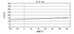
- FIGS. 4A to 4C are graphs showing experimental results of ESR in which the width W of the extraction electrode 123 was set as shown below in the crystal resonator element 12 used in FIG. 3B.
- 4A shows a shape in which the width W is 75 ⁇ m
- FIG. 4B shows a shape in which the width W gradually increases from 75 ⁇ m (L1) to 105 ⁇ m (L2)
- FIG. 4C shows a case in which the width W is 105 ⁇ m.
- the angle formed by the extraction electrode 123 with respect to the tangent to the connection position between the extraction electrode 123 and the mounting electrode 124 in FIG. 4B is in the range of 116 to 131 degrees.
- the ESR is significantly reduced compared to when the width W is constant at 75 ⁇ m. Also, compared with the case where the width W is constant at 105 ⁇ m, the ESR is lowered in the temperature range of about 0 to 100°C. As described above, it can be seen that the deterioration of the ESR of the crystal vibrating element 12 is effectively suppressed by widening the width W of the extraction electrode 123 while properly matching.
- the crystal vibrating element 12 of this embodiment includes a crystal blank 121 having a resonance frequency of 100 MHz or higher, two excitation electrodes 122 to which a voltage related to resonance of the crystal blank 121 is applied, and one end of the crystal blank 121. , two mounting electrodes 124 connected to the outside, and two extraction electrodes 123 connecting the excitation electrode 122 and the mounting electrode 124, respectively.
- the center of the excitation electrode 122 is positioned closer to the mounting electrode 124 than the center position of the crystal piece 121, and the two lead-out electrodes 123 are non-parallel and linear to each other between the excitation electrode 122 and the mounting electrode 124. connected.
- the extraction electrodes 123 can be efficiently shortened.
- the vibration does not largely protrude from the range of the excitation electrode 122. Therefore, even if the excitation electrode 122 and the mounting electrode 124 are brought close to each other with such a positional relationship, the mounting electrode does not respond to the vibration. Since the influence of 124 is suppressed to be small, it is possible to suppress the increase in ESR (CI) and to vibrate appropriately.
- the lead-out electrodes 123 are set in a non-parallel positional relationship, at least one of them (usually having the same shape and length) is tilted with respect to the vibration direction of the AT-cut crystal piece 121, so that the lead-out electrodes 123 can also reduce the influence on the vibration of In addition, since the extraction electrode 123 does not have a bent portion, it is possible to suppress signal reflection loss due to bending.
- the width of the extraction electrode 123 perpendicular to the extending direction from the excitation electrode 122 gradually increases from the connection position with the excitation electrode 122 toward the connection position with the mounting electrode 124 .
- an increase in ESR (CI) can be suppressed while matching impedance.
- the crystal resonator element 12 can appropriately suppress an increase in ESR (CI).
- the length of the long side (along the X-axis direction) of the crystal piece 121 is 1.4 mm or less. The above effect can be obtained remarkably when the size is appropriate for the crystal piece 121 of the crystal vibrating element 12 having a high resonance frequency of 100 MHz or more.
- the ratio of the length M1 between the center position of the excitation electrode 122 and the center position of the crystal blank 121 to the length of the long side of the crystal blank 121 is set to 0.393 or less. Such positioning effectively shortens the distance between the excitation electrode 122 and the mounting electrode 124 to shorten the length of the extraction electrode 123, thereby reducing the equivalent series resistance. Along with this, an increase in ESR (CI) can be suppressed, and the oscillation of the crystal blank 121 can be properly maintained.
- the crystal device 1 of the present embodiment includes the crystal oscillator 12 described above.
- accurate processing can be performed using a crystal oscillator 12 that operates more stably at an appropriate resonance frequency than before.
- excitation electrode 122 may not be perfectly circular.
- the excitation electrode 122 may be elliptical or square with rounded corners (rectangular, diamond-shaped, etc.) as desired. If the excitation electrode 122 is too small, the voltage amplitude required to obtain the necessary vibration will be large, which is inefficient.
- the size and shape of the crystal piece 121 may be appropriately adjusted according to the above conditions regarding the resonance frequency, the excitation electrode 122, and the like.
- the width of the lead-out electrode 123 need not be limited to that which simply gradually increases from the excitation electrode 122 toward the mounting electrode 124 .
- it may be adjusted as appropriate according to conditions such as spurious and fitting, and contents that are preferentially required for the crystal device 1 .
- crystal oscillator 12 may be sold or otherwise distributed separately from the substrate 11 or the like.
- specific configurations, structures, materials, and the like shown in the above embodiments can be changed as appropriate without departing from the gist of the present invention.
- the scope of the present invention includes the scope of the invention described in the claims and the scope of equivalents thereof.
- This invention can be used for crystal oscillators and crystal devices.
Abstract
Provided are a crystal oscillator and a crystal device with which an electrical signal that is in accordance with vibration can be obtained at a more appropriate ESR. A crystal oscillator (12) comprises: a crystal piece (121) that has a resonant frequency of 100 MHz or higher; two excitation electrodes (122) to which a voltage relating to the resonance of the crystal piece (121) is applied; two mounting electrodes (124) that are located offset toward the side of one end of the crystal piece (121), and are connected to an external part; and two extraction electrodes (123) that connect the respective excitation electrodes (122) and mounting electrodes (124). The centers of the excitation electrodes (122) are located further to the side that is close to the mounting electrodes (124) than the location of the center of the crystal piece (121), and the two extraction electrodes (123) are connected between the excitation electrodes (122) and the mounting electrodes (124) in straight lines that are not parallel to one another.
Description
本開示は、水晶振動素子及び水晶デバイスに関する。
The present disclosure relates to crystal oscillators and crystal devices.
水晶片を共振させて所望の周波数の信号を出力させる水晶振動素子では、振動が水晶片の縁などに達すると振動の質を低下させるので、水晶片の中心で振動させるように、水晶片の両面間で共振に係る電圧が印加される励振電極が位置している。共振周波数が高くなると、励振電極の平面視サイズを水晶片に比して小さくすることができる。この場合に、特開2017-050751号公報には、励振電極と外部接続のための搭載電極との間をつなぐ引き出し電極の引き出し方向を水晶片の振動に係るX軸(電気軸)方向に対して適宜な角度とすることで、等価直列抵抗(Equivalent Serial Resistance;ESR。又はCristal Impedance;CI)の上昇を抑制する技術が記載されている。
In a crystal resonator element that resonates a crystal blank to output a signal of a desired frequency, the quality of vibration deteriorates when the vibration reaches the edge of the crystal blank. An excitation electrode is located across which a voltage associated with resonance is applied. When the resonance frequency becomes high, the plane view size of the excitation electrode can be made smaller than that of the crystal piece. In this case, Japanese Patent Application Laid-Open No. 2017-050751 discloses that the extraction direction of extraction electrodes that connect the excitation electrodes and the mounting electrodes for external connection is set with respect to the X-axis (electrical axis) direction related to the vibration of the crystal piece. Equivalent Serial Resistance (ESR) or Crystal Impedance (CI) is suppressed from increasing by setting an appropriate angle.
本開示の一の態様は、
共振周波数が100MHz以上の水晶片と、
前記水晶片の共振に係る電圧が印加される2つの励振電極と、
前記水晶片の一端の側に寄って位置し、外部に接続される2つの搭載電極と、
前記励振電極と前記搭載電極とをそれぞれつなぐ2本の引き出し電極と、
を備え、
前記励振電極の中心は、前記水晶片の中心位置よりも前記搭載電極に近い側に位置し、
前記2本の引き出し電極は、前記励振電極と前記搭載電極との間を互いに非平行かつ直線でつないでいる
水晶振動素子である。 One aspect of the present disclosure is
a crystal piece having a resonance frequency of 100 MHz or higher;
two excitation electrodes to which a voltage related to resonance of the crystal piece is applied;
two mounting electrodes located close to one end of the crystal piece and connected to the outside;
two extraction electrodes respectively connecting the excitation electrodes and the mounting electrodes;
with
the center of the excitation electrode is positioned closer to the mounting electrode than the center position of the crystal blank,
The two extraction electrodes are crystal vibrating elements that connect the excitation electrodes and the mounting electrodes in non-parallel and straight lines.
以下、実施の形態を図面に基づいて説明する。
図1A及び図1Bは、本実施形態の水晶デバイス1の構成を示す図である。図1Aは、蓋体14を外した状態で示した斜視図であり、図1Bは、図1Aにおける断面線AAでの断面図である。
水晶デバイス1は、基体11と、水晶振動素子12と、導電性接着剤13と、蓋体14と、部品15などを備える。 Embodiments will be described below with reference to the drawings.
1A and 1B are diagrams showing the configuration of acrystal device 1 of this embodiment. 1A is a perspective view showing a state in which the lid body 14 is removed, and FIG. 1B is a cross-sectional view taken along the cross-sectional line AA in FIG. 1A.
Thecrystal device 1 includes a base 11, a crystal vibrating element 12, a conductive adhesive 13, a lid 14, parts 15, and the like.
図1A及び図1Bは、本実施形態の水晶デバイス1の構成を示す図である。図1Aは、蓋体14を外した状態で示した斜視図であり、図1Bは、図1Aにおける断面線AAでの断面図である。
水晶デバイス1は、基体11と、水晶振動素子12と、導電性接着剤13と、蓋体14と、部品15などを備える。 Embodiments will be described below with reference to the drawings.
1A and 1B are diagrams showing the configuration of a
The
基体11は、底板111と、底板111の上面の周縁部に位置する側壁部112とを有し、これら底板111と側壁部112とにより囲まれた凹部11aを有する箱形形状である。凹部11aの底面には、電極パッド113が位置している。また、底板111の裏面(-z側の面)には、外部接続パッド114が位置している。なお、図では説明のために底板111と側壁部112との間に点線を示しているが、これらは実際には一体のものである。
The base 11 has a bottom plate 111 and side walls 112 positioned on the periphery of the upper surface of the bottom plate 111, and has a box-like shape with a recess 11a surrounded by the bottom plate 111 and the side walls 112. An electrode pad 113 is positioned on the bottom surface of the recess 11a. In addition, external connection pads 114 are located on the back surface (surface on the −z side) of the bottom plate 111 . In the drawing, a dotted line is shown between the bottom plate 111 and the side wall portion 112 for the sake of explanation, but they are actually integrated.
電極パッド113には、導電性接着剤13を介して水晶振動素子12が接続されている。電極パッド113は、基体11の内部に位置する図示略の電気配線を介して外部接続パッド114との間で電気的につながっている。なお、電極パッド113は、底板111の上面に位置する突出部分上に位置しているものであってもよい。
The crystal vibrating element 12 is connected to the electrode pad 113 via the conductive adhesive 13 . The electrode pads 113 are electrically connected to external connection pads 114 via electrical wiring (not shown) located inside the base 11 . Note that the electrode pads 113 may be positioned on the projecting portion positioned on the upper surface of the bottom plate 111 .
外部接続パッド114は、モジュール用基板などに、例えばはんだなどを用いて接続されて、外部のモジュール用基板などとの間で水晶デバイス1の信号の送受信を可能とされる。
The external connection pads 114 are connected to the module board or the like using, for example, solder, so that the crystal device 1 can transmit and receive signals to and from the external module board and the like.
水晶振動素子12は、水晶片121と、励振電極122と、引き出し電極123と、搭載電極124などを有する。搭載電極124は、水晶振動素子12を基体11に搭載するための電極であって、水晶片121の+x側の端に寄って、ここでは、2つの(一対の)搭載電極1241、1242がそれぞれ+x側の端に接して位置し、各々導電性接着剤13を介して電極パッド113に接続、固定されている。これにより、励振電極122が電極パッド113及び外部接続パッド114を介して外部につながる。このように、水晶振動素子12は、片持ち状態である。
The crystal vibrating element 12 has a crystal piece 121, an excitation electrode 122, an extraction electrode 123, a mounting electrode 124, and the like. The mounting electrode 124 is an electrode for mounting the crystal vibrating element 12 on the base 11, and near the end of the crystal piece 121 on the +x side, here, two (a pair of) mounting electrodes 1241 and 1242 are respectively mounted. They are positioned in contact with the ends on the +x side and are connected and fixed to the electrode pads 113 via the conductive adhesive 13 . Thereby, the excitation electrode 122 is connected to the outside through the electrode pad 113 and the external connection pad 114 . Thus, the crystal vibrating element 12 is in a cantilevered state.
励振電極122は、水晶片121の下面側(底板111と対向する側、-z側)の励振電極1221と、上面側(+z側)の励振電極1222との2つを有する。これら2つの励振電極122は、ここでは、上面側から見た平面視で同一位置にある。励振電極1221は、引き出し電極1231を介して搭載電極1241に電気的につながっている。励振電極1222は、引き出し電極1232を介して搭載電極1242に電気的につながっている。上面側に位置する引き出し電極1232につながっている搭載電極1242は、上下両面にわたって広がっている。これにより、外部接続パッド114と励振電極122との間がそれぞれ水晶振動素子12の下面側で導電性接着剤13を介して接続され、共振に係る電圧が印加される。すなわち、励振電極122には、電圧信号が励振電極122に印加されて水晶片121を振動させ(励振し)たり、励振電極122の間に生じた電圧が外部接続パッド114へ出力されたりする。
The excitation electrode 122 has two excitation electrodes 1221 on the lower surface side of the crystal piece 121 (the side facing the bottom plate 111, -z side) and an excitation electrode 1222 on the upper surface side (+z side). These two excitation electrodes 122 are located at the same position in plan view from the upper surface side. The excitation electrode 1221 is electrically connected to the mounting electrode 1241 via the extraction electrode 1231 . The excitation electrode 1222 is electrically connected to the mounting electrode 1242 via the extraction electrode 1232 . A mounting electrode 1242 connected to the extraction electrode 1232 located on the upper surface side spreads over both upper and lower surfaces. As a result, the external connection pad 114 and the excitation electrode 122 are connected to each other via the conductive adhesive 13 on the lower surface side of the crystal vibrating element 12, and a voltage for resonance is applied. That is, a voltage signal is applied to the excitation electrodes 122 to vibrate (excite) the crystal blank 121 , or a voltage generated between the excitation electrodes 122 is output to the external connection pads 114 .
水晶片121は、例えば、ATカットによる矩形状のものであり、出力対象の共振周波数に応じた厚さを有する。通常、共振周波数が高くなるほど水晶片121が薄くなる。特には限られないが、ここでは、水晶片121は、共振周波数が100MHz又はこれ以上である。なお、水晶片121は、全体が均一の厚さであるものに限られない。振動を生じる励振電極122との接触範囲及びその周辺(これらを振動部と記す)の厚さに比して、搭載電極124の部分が厚くなっていてもよく、また、水晶片121は、更に上記振動部を取り囲む相対的に厚い部分を有していてもよい。あるいは反対に、水晶片121は、振動部に比して周囲が相対的に薄い形状を有していてもよい。水晶片121の結晶軸(電気軸)に沿った方向(X軸方向)が図のx軸方向と一致しており、当該X軸方向に伸びる辺が矩形形状(長方形)の長辺となっている。
The crystal piece 121 is, for example, an AT-cut rectangular piece, and has a thickness corresponding to the resonance frequency to be output. Normally, the higher the resonance frequency, the thinner the crystal piece 121 becomes. Although not particularly limited, here, the crystal piece 121 has a resonance frequency of 100 MHz or higher. Note that the crystal piece 121 is not limited to having a uniform thickness as a whole. The portion of the mounting electrode 124 may be thicker than the thickness of the contact area with the excitation electrode 122 that causes vibration and the thickness of the surrounding area (these are referred to as a vibrating portion). It may have a relatively thick portion surrounding the vibrating portion. Alternatively, conversely, crystal piece 121 may have a shape in which the periphery is relatively thin compared to the vibrating portion. The direction (X-axis direction) along the crystal axis (electrical axis) of the crystal blank 121 coincides with the x-axis direction in the drawing, and the sides extending in the X-axis direction are the long sides of the rectangular shape (rectangle). there is
基体11の凹部11aを取り囲む側壁部112の上端面には、蓋体14がろう材などによって接合されている。側壁部112と蓋体14との間には、平面視で側壁部112と略同一形状である枠状の導体であるメタライズ層(不図示)が位置していてもよい。メタライズ層は、塗布焼成された導体層であってもよいし、めっき層などであってもよい。蓋体14により凹部11aが封止されて、外部との空気や埃などの出入りが遮断される。基体11及び蓋体14が本実施形態の水晶デバイス1において水晶振動素子12を内部に収容する筐体である。
A lid 14 is joined to the upper end surface of the side wall portion 112 surrounding the concave portion 11a of the base 11 with a brazing material or the like. Between the side wall portion 112 and the lid 14, a metallized layer (not shown), which is a frame-shaped conductor and has substantially the same shape as the side wall portion 112 in plan view, may be positioned. The metallized layer may be a conductive layer obtained by coating and firing, or may be a plated layer. The recessed portion 11a is sealed by the lid 14 to block entry and exit of air, dust, and the like with the outside. The base 11 and the lid 14 are a housing that accommodates the crystal vibrating element 12 in the crystal device 1 of this embodiment.
部品15は、基体11の底面側に位置している。部品15は、ICチップなどの電子部品であってもよいし、検温素子(サーミスタなど)といったセンサなどであってもよい。また、部品15は、同一種類又は複数種類の複数個の組合せであってもよい。これらは、水晶振動素子12の共振周波数の調整に係る付帯情報を出力したり、あるいは、付帯情報に応じた調整を行ったりするものであり、すなわち水晶デバイス1は、水晶発振器であってもよい。なお、部品15の位置は、底面の平面視中央付近ではなく、偏った位置であってもよい。
The part 15 is positioned on the bottom side of the base 11 . The component 15 may be an electronic component such as an IC chip, or may be a sensor such as a temperature detecting element (thermistor, etc.). Also, the parts 15 may be of the same type or a combination of multiple types. These are for outputting supplementary information relating to adjustment of the resonance frequency of the crystal oscillator 12, or performing adjustment according to the supplementary information. That is, the crystal device 1 may be a crystal oscillator. . Note that the position of the component 15 may not be near the center of the bottom surface in plan view, but may be at a deviated position.
ここでは、基体11は、特には限られないが、例えば、セラミック材料、半導体材料、ガラス材料若しくは水晶、又はこれらの組合せであり、内部や表面などに導体の信号線(電力供給及び接地に係るものを含む)を有する。導電性の電極パッド113は、例えば、基体11上に印刷されたものであってもよく、また、その最上面には、例えば、金めっきなどがなされていてもよい。
また、導電性接着剤13は、例えば、銀フィラーを含有する樹脂系(シリコーン系樹脂又はエポキシ樹脂など)の接着剤であってもよい。特に、シリコーン系樹脂の導電性接着剤13は、接着後にも柔らかいので、振動に対して悪影響を与えづらい。
また、蓋体14は金属導体の平板であり、例えば、鉄、銅、ニッケル、クロム、コバルト、モリブデン若しくはタングステンを含む金属、又はこれらの合金である。 Here, thesubstrate 11 is not particularly limited, but may be, for example, a ceramic material, a semiconductor material, a glass material, or a crystal, or a combination thereof. (including things). The conductive electrode pads 113 may be printed on the substrate 11, for example, and the uppermost surface thereof may be plated with gold, for example.
Also, theconductive adhesive 13 may be, for example, a resin-based (silicone-based resin, epoxy resin, or the like) adhesive containing a silver filler. In particular, the conductive adhesive 13 made of silicone resin is soft even after being adhered, so it is less likely to adversely affect vibrations.
Also, thelid 14 is a metal conductor flat plate, for example, a metal containing iron, copper, nickel, chromium, cobalt, molybdenum or tungsten, or an alloy thereof.
また、導電性接着剤13は、例えば、銀フィラーを含有する樹脂系(シリコーン系樹脂又はエポキシ樹脂など)の接着剤であってもよい。特に、シリコーン系樹脂の導電性接着剤13は、接着後にも柔らかいので、振動に対して悪影響を与えづらい。
また、蓋体14は金属導体の平板であり、例えば、鉄、銅、ニッケル、クロム、コバルト、モリブデン若しくはタングステンを含む金属、又はこれらの合金である。 Here, the
Also, the
Also, the
次に、本実施形態の水晶振動素子12についてより詳しく説明する。
図2は、本実施形態の水晶デバイス1の蓋体14を外した状態での平面図である。なお、上面側から見えない一部の構成が破線で示されている。また、点線は、水晶振動素子12のx軸方向(長辺に沿った方向)について中央を示す。 Next, thecrystal resonator element 12 of this embodiment will be described in more detail.
FIG. 2 is a plan view of thecrystal device 1 of this embodiment with the cover 14 removed. A portion of the configuration that cannot be seen from the top side is indicated by a dashed line. A dotted line indicates the center of the crystal vibrating element 12 in the x-axis direction (direction along the long side).
図2は、本実施形態の水晶デバイス1の蓋体14を外した状態での平面図である。なお、上面側から見えない一部の構成が破線で示されている。また、点線は、水晶振動素子12のx軸方向(長辺に沿った方向)について中央を示す。 Next, the
FIG. 2 is a plan view of the
水晶振動素子12の励振電極122は、ここでは、円形である。また、この励振電極122の中心位置は、水晶振動素子12の中心位置よりも搭載電極124の側に寄って位置している。励振電極122は、100MHz以上の共振周波数では、水晶片121の振動部と同程度又はやや小さい面積である。この面積が水晶片121の面積に近いと、水晶片121の端部の影響を受けて振動の特性が低下する。また、振動は、励振電極122の角によってもその振動特性に影響を受ける。ここでは、励振電極122の角を丸めて特に平面視円形とすることで、上記振動特性への悪影響を低減する。
The excitation electrode 122 of the crystal vibrating element 12 is here circular. Further, the center position of the excitation electrode 122 is closer to the mounting electrode 124 side than the center position of the crystal vibrating element 12 . The excitation electrode 122 has an area approximately equal to or slightly smaller than that of the vibrating portion of the crystal piece 121 at a resonance frequency of 100 MHz or more. If this area is close to the area of the crystal piece 121, the vibration characteristics are degraded due to the influence of the edge of the crystal piece 121. FIG. The vibration characteristics are also affected by the angle of the excitation electrode 122 . Here, by rounding the corners of the excitation electrode 122 to make it particularly circular in plan view, the adverse effect on the vibration characteristics is reduced.
なお、共振周波数が100MHz以上と高い場合には、これに従って水晶片121のx軸方向(すなわちX軸方向)についての長さも短くすることができるが、必ずしも短くなくてもよい。ここでは、水晶片121のx軸方向についての辺(長辺)の長さは、例えば、0.8~1.4mmの範囲とされ得る。また、水晶片121のy軸方向についての辺(短辺)の長さは、例えば、0.4~1.0mmの範囲とされ得る。
When the resonance frequency is as high as 100 MHz or higher, the length of the crystal blank 121 in the x-axis direction (that is, the X-axis direction) can be shortened accordingly, but it does not necessarily have to be shortened. Here, the length of the side (long side) of the crystal piece 121 in the x-axis direction can be in the range of 0.8 to 1.4 mm, for example. Also, the length of the side (short side) of the crystal blank 121 in the y-axis direction can be in the range of 0.4 to 1.0 mm, for example.
このようなサイズの励振電極122の中心が、搭載電極124などの振動への影響を抑えるために従来のように当該搭載電極124から離れた位置にあると、その分引き出し電極1231、1232(まとめて2本の引き出し電極123)が長くなる。引き出し電極123は、励振電極122や搭載電極124などと比較して細いので、これが長くなるとESR(CI)の上昇などにつながる。上記のように、100MHz以上の共振周波数を有する水晶振動素子12では、励振電極122の範囲外に振動が大きく広がらないので、搭載電極124などから励振電極122を離隔させるメリットよりも引き出し電極123が長くなるデメリットの方が大きくなる。そこで、この水晶振動素子12では、励振電極122の平面視中心位置を水晶片121の平面視中心位置よりも搭載電極124に近い位置としている。励振電極122の平面視中心位置と水晶片121の平面視中心位置との間の長さM1(距離)は、通常、0μmよりも大きく550μmより小さく、好ましくは、0μmよりも大きく540μm以下であり、特に好ましくは、0μmよりも大きく440μm以下である。水晶片121のx軸方向についての辺(長辺)の長さに対する長さM1の比は、通常0.393以下であり、好ましくは0.386以下であり、特に好ましくは0.315以下である。なお、励振電極122が小さすぎると、必要な振動を得るのに必要な電圧振幅が大きくなり、効率がよくないので、適宜なサイズとされる。励振電極122が円形である場合には、励振電極122の内径(直径)は、通常150μm以上900μm以下であり、好ましくは、160μm以上600μm以下であり、特に好ましくは、170μm以上400μm以下である。水晶片121の振動部に対する励振電極122の平面視における面積比は、通常0.005以上0.785以下であり、好ましくは、0.060以上0.500以下であり、特に好ましくは、0.070以上0.130以下である。
If the center of the excitation electrode 122 having such a size is positioned away from the mounting electrode 124 in order to suppress the influence on the vibration of the mounting electrode 124 and the like as in the conventional art, the extraction electrodes 1231 and 1232 (summarization) , the two lead-out electrodes 123) become longer. Since the lead-out electrode 123 is thinner than the excitation electrode 122, the mounting electrode 124, etc., if it becomes longer, it leads to an increase in ESR (CI). As described above, in the crystal vibrating element 12 having a resonance frequency of 100 MHz or more, the vibration does not spread outside the range of the excitation electrodes 122. Therefore, the extraction electrodes 123 are not advantageous in separating the excitation electrodes 122 from the mounting electrodes 124 and the like. The disadvantage of being longer is greater. Therefore, in this crystal vibrating element 12 , the center position of the excitation electrode 122 in plan view is closer to the mounting electrode 124 than the center position of the crystal piece 121 in plan view. The length M1 (distance) between the center position of the excitation electrode 122 and the center position of the crystal piece 121 in plan view is usually greater than 0 μm and less than 550 μm, preferably greater than 0 μm and less than or equal to 540 μm. , particularly preferably larger than 0 μm and 440 μm or less. The ratio of the length M1 to the length of the side (long side) of the crystal piece 121 in the x-axis direction is usually 0.393 or less, preferably 0.386 or less, and particularly preferably 0.315 or less. be. If the excitation electrode 122 is too small, the voltage amplitude required to obtain the necessary vibration will be large, resulting in poor efficiency. When the excitation electrode 122 is circular, the inner diameter (diameter) of the excitation electrode 122 is usually 150 μm or more and 900 μm or less, preferably 160 μm or more and 600 μm or less, and particularly preferably 170 μm or more and 400 μm or less. The area ratio of the excitation electrode 122 to the vibrating portion of the crystal element 121 in plan view is usually 0.005 or more and 0.785 or less, preferably 0.060 or more and 0.500 or less, and particularly preferably 0.060 or more and 0.500 or less. 070 or more and 0.130 or less.
また、この水晶振動素子12では、2本の引き出し電極123は互いに非平行であり、かつ矩形状の搭載電極124における励振電極122の側の辺E1に対して傾いた方向に伸びる直線状である。引き出し電極123が曲がり部分を有さないことで、搭載電極124と励振電極122の各接続点間を短く結ぶことができる。搭載電極124が水晶片121の短辺側に寄って位置する場合、水晶片121の短辺に対する辺E1の比は、通常0.10以上0.50より小さく、好ましくは、0.18以上0.45以下であり、特に好ましくは、0.20以上0.40以下である。また、周波数が高い場合には、引き出し電極123の折れ曲がりによる信号の反射が無視できなくなるので、直線状とすることで、ESRを改善することができる。また、特に励振電極122が円形などで縁が曲線状の場合には、辺E1に垂直な向きよりも、曲率中心方向から放射状に伸びる向きに近い方が引き出し電極123の長さが適切に調整されやすい。また、辺E1に垂直な方向、すなわちx方向に引き出し電極123が伸びないことで、水晶片121の振動に対する影響を低減することができる。なお、引き出し電極123がx方向に平行でなければ、傾きの角度φの大小はESRの改善などにはあまり影響がない。特には限られないが、例えば、角度φは115~130度程度である。
Further, in the crystal vibrating element 12, the two lead-out electrodes 123 are non-parallel to each other, and are straight lines extending in a direction inclined with respect to the side E1 of the rectangular mounting electrode 124 on the excitation electrode 122 side. . Since the lead-out electrode 123 does not have a bent portion, it is possible to shorten the connection points between the mounting electrodes 124 and the excitation electrodes 122 . When the mounting electrode 124 is located close to the short side of the crystal piece 121, the ratio of the side E1 to the short side of the crystal piece 121 is usually 0.10 or more and less than 0.50, preferably 0.18 or more and 0.50. 0.45 or less, and particularly preferably 0.20 or more and 0.40 or less. In addition, when the frequency is high, the reflection of the signal due to the bending of the extraction electrode 123 cannot be ignored. In particular, when the excitation electrode 122 is circular and has a curved edge, the length of the lead-out electrode 123 is appropriately adjusted when the direction radially extending from the center of curvature is closer to the direction perpendicular to the side E1 than the direction perpendicular to the side E1. easy to be In addition, since the lead-out electrode 123 does not extend in the direction perpendicular to the side E1, ie, in the x-direction, the influence on the vibration of the crystal piece 121 can be reduced. If the lead-out electrode 123 is not parallel to the x-direction, the magnitude of the inclination angle φ has little effect on the improvement of the ESR. Although not particularly limited, the angle φ is, for example, about 115 to 130 degrees.
また、引き出し電極123において、その延在方向に垂直な幅Wは、励振電極122との接続位置から当該接続位置での幅L1に対して搭載電極124との接続位置に向けて、幅L2へと漸増していてもよい。単純には、引き出し電極123が太い方がESR(CI)の増加が抑えられるが、励振電極122の直近で引き出し電極123が太いと、水晶片121の振動に影響を与える影響の方が大きくなって、理想通りにはESRは低下しない。また、高周波数帯の信号伝送では、配線途中に急激な(不連続な)幅の変化があると、特性インピーダンスのミスマッチが生じ、配線抵抗が増大しやすい。また、スプリアスやフィッティングの悪化にもつながり得る。また、搭載電極124と励振電極122との間でもインピーダンス整合を取る必要がある。したがって、引き出し電極123の幅が励振電極122との接続位置から搭載電極124との接続位置に向けて漸増することで、ESRの増大を抑えつつ適切にインピーダンス整合を取ることができる。
In addition, the width W of the lead-out electrode 123 perpendicular to the extending direction varies from the width L1 at the connection position from the connection position with the excitation electrode 122 to the width L2 toward the connection position with the mounting electrode 124. and may be gradually increased. Simply put, the thicker the lead-out electrode 123 is, the more the increase in ESR (CI) can be suppressed. Therefore, ideally, the ESR does not decrease. Further, in high-frequency band signal transmission, if there is a sudden (discontinuous) width change in the middle of the wiring, a characteristic impedance mismatch will occur, and the wiring resistance will tend to increase. It can also lead to spurious emissions and deterioration of fitting. Also, it is necessary to match the impedance between the mounting electrode 124 and the excitation electrode 122 . Therefore, by gradually increasing the width of the extraction electrode 123 from the connection position with the excitation electrode 122 toward the connection position with the mounting electrode 124, it is possible to appropriately match the impedance while suppressing an increase in ESR.
幅Wが励振電極122との接続位置での幅L1から搭載電極124との接続位置での幅L2へと漸増する場合、励振電極122との接続位置での幅L1は、辺E1より短ければ特段の制限はないが、通常30μm以上180μm以下であり、好ましくは、35μm以上150μm以下であり、特に好ましくは、40μm以上120μm以下である。辺E1に対する幅L1の比は、通常0.15以上1よりも小さく、好ましくは0.2以上0.9以下であり、特に好ましくは0.3以上0.8以下である。
When the width W gradually increases from the width L1 at the connection position with the excitation electrode 122 to the width L2 at the connection position with the mounting electrode 124, the width L1 at the connection position with the excitation electrode 122 is shorter than the side E1. Although there is no particular limitation, it is usually 30 μm or more and 180 μm or less, preferably 35 μm or more and 150 μm or less, and particularly preferably 40 μm or more and 120 μm or less. The ratio of the width L1 to the side E1 is usually 0.15 or more and less than 1, preferably 0.2 or more and 0.9 or less, and particularly preferably 0.3 or more and 0.8 or less.
搭載電極124との接続位置での幅L2は、幅L1よりも長くかつ辺E1以下であれば特段の制限はないが、通常30μm以上180μm以下であり、好ましくは35μm以上150μm以下であり、特に好ましくは40μm以上120μm以下である。辺E1に対する励振電極122の幅(方形の場合には水晶片121の短辺に平行な向きの辺、円形の場合には直径)の比は、通常0.03以上0.50以下、好ましくは、0.10以上0.45以下、特に好ましくは、0.20以上0.40以下である。
Width L2 at the connection position with mounting electrode 124 is not particularly limited as long as it is longer than width L1 and equal to or less than side E1. It is preferably 40 μm or more and 120 μm or less. The ratio of the width of the excitation electrode 122 to the side E1 (the side parallel to the short side of the crystal piece 121 in the case of a square, the diameter in the case of a circle) is usually 0.03 or more and 0.50 or less, preferably , 0.10 or more and 0.45 or less, particularly preferably 0.20 or more and 0.40 or less.
幅L2に対する幅L1の比は、通常0.15以上1より小さく、好ましくは、0.2以上0.9以下、特に好ましくは、0.3以上0.8以下である。幅L1に対する幅L2の比が上述の範囲にあることは、スプリアス振動が生じにくく、配線抵抗が増加しにくい点で好ましい。
The ratio of width L1 to width L2 is usually 0.15 or more and less than 1, preferably 0.2 or more and 0.9 or less, and particularly preferably 0.3 or more and 0.8 or less. It is preferable that the ratio of the width L2 to the width L1 is within the above range, since spurious vibration is less likely to occur and wiring resistance is less likely to increase.
図3A及び図3Bは、引き出し電極123の折れ曲がりの有無に応じたESRの温度特性を示す実験結果である。
この実験では、水晶片121(長辺1166μm、短辺787μm)が330μm径の円状の励振電極122に応じた振動部(長辺350μm、短辺350μm)を有し、励振電極122の平面視中心位置と水晶片121の平面視中心位置との間の長さM1は、170μmである。振動電極122のの搭載電極124からの距離が異なり、励振電極122及び搭載電極124(辺E1:180μm)の同一位置に幅75μmの引き出し電極123がそれぞれ接続している。励振電極122との接続位置から伸びる引き出し電極123の向きと搭載電極124の接続位置における接線との角度は、125度である。図3Aでは、上記距離が長く、引き出し電極123が折れ曲がり有して辺E1に対して垂直に接続している。図3Bでは、上記距離が短く、引き出し電極123を折れ曲がりなしで辺E1に対して直接斜めに接続している。図3Aと図3Bとでは、引き出し電極の1本当たりで約190μmの長さの差が生じている。電極及び引き出し電極の厚さはそれぞれ210nmである。 3A and 3B are experimental results showing temperature characteristics of ESR depending on whether or not theextraction electrode 123 is bent.
In this experiment, the crystal piece 121 (long side 1166 μm, short side 787 μm) has a vibrating portion (long side 350 μm, short side 350 μm) corresponding to thecircular excitation electrode 122 having a diameter of 330 μm. A length M1 between the center position and the center position of the crystal piece 121 in plan view is 170 μm. The distance from the mounting electrode 124 of the vibration electrode 122 is different, and the extraction electrode 123 with a width of 75 μm is connected to the same position of the excitation electrode 122 and the mounting electrode 124 (side E1: 180 μm). The angle between the direction of the extraction electrode 123 extending from the connection position with the excitation electrode 122 and the tangential line at the connection position with the mounting electrode 124 is 125 degrees. In FIG. 3A, the distance is long, and the extraction electrode 123 is bent and connected perpendicularly to the side E1. In FIG. 3B, the distance is short, and the extraction electrode 123 is connected directly obliquely to the side E1 without bending. Between FIG. 3A and FIG. 3B, there is a length difference of about 190 μm per lead electrode. The thickness of the electrode and extraction electrode is 210 nm each.
この実験では、水晶片121(長辺1166μm、短辺787μm)が330μm径の円状の励振電極122に応じた振動部(長辺350μm、短辺350μm)を有し、励振電極122の平面視中心位置と水晶片121の平面視中心位置との間の長さM1は、170μmである。振動電極122のの搭載電極124からの距離が異なり、励振電極122及び搭載電極124(辺E1:180μm)の同一位置に幅75μmの引き出し電極123がそれぞれ接続している。励振電極122との接続位置から伸びる引き出し電極123の向きと搭載電極124の接続位置における接線との角度は、125度である。図3Aでは、上記距離が長く、引き出し電極123が折れ曲がり有して辺E1に対して垂直に接続している。図3Bでは、上記距離が短く、引き出し電極123を折れ曲がりなしで辺E1に対して直接斜めに接続している。図3Aと図3Bとでは、引き出し電極の1本当たりで約190μmの長さの差が生じている。電極及び引き出し電極の厚さはそれぞれ210nmである。 3A and 3B are experimental results showing temperature characteristics of ESR depending on whether or not the
In this experiment, the crystal piece 121 (long side 1166 μm, short side 787 μm) has a vibrating portion (long side 350 μm, short side 350 μm) corresponding to the
折れ曲がりのない引き出し電極123が、直接斜めに搭載電極124の辺E1と励振電極122とをつなぐことで、ESRが低下しており、製品の質として許容される20Ωを十分に下回っていることが分かる。
The unbent lead-out electrode 123 directly and obliquely connects the side E1 of the mounting electrode 124 and the excitation electrode 122, thereby lowering the ESR, which is sufficiently below 20Ω which is acceptable for product quality. I understand.
図4A~図4Cは、図3Bで使用した水晶振動素子12において、引き出し電極123の幅Wを以下に示すように設定したESRの実験結果を示すグラフである。図4Aは、幅Wが75μm、図4Bは、幅Wが75μm(L1)から105μm(L2)へ漸増する形状、図4Cは、幅Wが105μmの場合を示す。図4Bにおける引き出し電極123と搭載電極124との接続位置の接線に対する当該引き出し電極123のなす角は、116~131度の範囲である。
4A to 4C are graphs showing experimental results of ESR in which the width W of the extraction electrode 123 was set as shown below in the crystal resonator element 12 used in FIG. 3B. 4A shows a shape in which the width W is 75 μm, FIG. 4B shows a shape in which the width W gradually increases from 75 μm (L1) to 105 μm (L2), and FIG. 4C shows a case in which the width W is 105 μm. The angle formed by the extraction electrode 123 with respect to the tangent to the connection position between the extraction electrode 123 and the mounting electrode 124 in FIG. 4B is in the range of 116 to 131 degrees.
幅Wを75-105μmで変化させると、幅Wが75μmで一定の場合と比較して、ESRが顕著に低下することが分かる。また、幅Wが105μmで一定の場合と比較しても、温度が0-100℃程度の範囲ではESRの低下がみられる。このように、適切に整合を取りつつ引き出し電極123の幅Wを広げることで、水晶振動素子12のESRの悪化を効果的に抑制していることが分かる。
It can be seen that when the width W is varied from 75 to 105 μm, the ESR is significantly reduced compared to when the width W is constant at 75 μm. Also, compared with the case where the width W is constant at 105 μm, the ESR is lowered in the temperature range of about 0 to 100°C. As described above, it can be seen that the deterioration of the ESR of the crystal vibrating element 12 is effectively suppressed by widening the width W of the extraction electrode 123 while properly matching.
以上のように、本実施形態の水晶振動素子12は、共振周波数が100MHz以上の水晶片121と、水晶片121の共振に係る電圧が印加される2つの励振電極122と、水晶片121の一端の側に寄って位置し、外部に接続される2つの搭載電極124と、励振電極122と搭載電極124とをそれぞれつなぐ2本の引き出し電極123と、を備える。励振電極122の中心は、水晶片121の中心位置よりも搭載電極124に近い側に位置し、2本の引き出し電極123は、励振電極122と搭載電極124との間を互いに非平行かつ直線でつないでいる。
このような励振電極122の位置取りにより、引き出し電極123を効率的に短くすることができる。高周波数の共振周波数を有する水晶振動素子12では、励振電極122の範囲から振動が大きくはみ出さないので、このような位置関係として、励振電極122と搭載電極124を近づけても、振動に対する搭載電極124の影響は小さく抑えられるので、ESR(CI)の上昇を抑制して適切に振動させることができる。また、このときに引き出し電極123を非平行な位置関係とすることで、ATカットの水晶片121の振動方向に対して少なくとも一方(通常は同一形状同一長なので両方)が傾くので、引き出し電極123の振動に対する影響も低減させることができる。また、引き出し電極123が折り曲げ箇所を有しないことで、折り曲げによる信号の反射損失を抑えることができる。 As described above, thecrystal vibrating element 12 of this embodiment includes a crystal blank 121 having a resonance frequency of 100 MHz or higher, two excitation electrodes 122 to which a voltage related to resonance of the crystal blank 121 is applied, and one end of the crystal blank 121. , two mounting electrodes 124 connected to the outside, and two extraction electrodes 123 connecting the excitation electrode 122 and the mounting electrode 124, respectively. The center of the excitation electrode 122 is positioned closer to the mounting electrode 124 than the center position of the crystal piece 121, and the two lead-out electrodes 123 are non-parallel and linear to each other between the excitation electrode 122 and the mounting electrode 124. connected.
By positioning theexcitation electrodes 122 in this manner, the extraction electrodes 123 can be efficiently shortened. In the crystal vibrating element 12 having a high resonance frequency, the vibration does not largely protrude from the range of the excitation electrode 122. Therefore, even if the excitation electrode 122 and the mounting electrode 124 are brought close to each other with such a positional relationship, the mounting electrode does not respond to the vibration. Since the influence of 124 is suppressed to be small, it is possible to suppress the increase in ESR (CI) and to vibrate appropriately. At this time, by setting the lead-out electrodes 123 in a non-parallel positional relationship, at least one of them (usually having the same shape and length) is tilted with respect to the vibration direction of the AT-cut crystal piece 121, so that the lead-out electrodes 123 can also reduce the influence on the vibration of In addition, since the extraction electrode 123 does not have a bent portion, it is possible to suppress signal reflection loss due to bending.
このような励振電極122の位置取りにより、引き出し電極123を効率的に短くすることができる。高周波数の共振周波数を有する水晶振動素子12では、励振電極122の範囲から振動が大きくはみ出さないので、このような位置関係として、励振電極122と搭載電極124を近づけても、振動に対する搭載電極124の影響は小さく抑えられるので、ESR(CI)の上昇を抑制して適切に振動させることができる。また、このときに引き出し電極123を非平行な位置関係とすることで、ATカットの水晶片121の振動方向に対して少なくとも一方(通常は同一形状同一長なので両方)が傾くので、引き出し電極123の振動に対する影響も低減させることができる。また、引き出し電極123が折り曲げ箇所を有しないことで、折り曲げによる信号の反射損失を抑えることができる。 As described above, the
By positioning the
また、引き出し電極123の励振電極122からの延在方向に垂直な幅は、励振電極122との接続位置から搭載電極124との接続位置へ向けて漸増している。これによりインピーダンスの整合を取りつつESR(CI)の増加を抑えることができる。特に、インピーダンスなどに応じて6-7倍程度の範囲内で幅を漸増させることで、水晶振動素子12は、適切にESR(CI)の増加を抑えることができる。
In addition, the width of the extraction electrode 123 perpendicular to the extending direction from the excitation electrode 122 gradually increases from the connection position with the excitation electrode 122 toward the connection position with the mounting electrode 124 . Thereby, an increase in ESR (CI) can be suppressed while matching impedance. In particular, by gradually increasing the width within a range of about 6 to 7 times depending on the impedance or the like, the crystal resonator element 12 can appropriately suppress an increase in ESR (CI).
また、水晶片121の長辺の(X軸方向に沿った)長さは1.4mm以下である。100MHz以上の高周波数の共振周波数を有する水晶振動素子12の水晶片121に対して適切なサイズの場合に、上記効果が顕著に得られる。
Also, the length of the long side (along the X-axis direction) of the crystal piece 121 is 1.4 mm or less. The above effect can be obtained remarkably when the size is appropriate for the crystal piece 121 of the crystal vibrating element 12 having a high resonance frequency of 100 MHz or more.
また、水晶片121の長辺の長さに対する励振電極122の中心位置と水晶片121の中心位置との間の長さM1の比を0.393以下とする。このような位置取りにより、効果的に励振電極122と搭載電極124との距離を短縮して引き出し電極123を短くして、等価直列抵抗の低下を図る。これとともに、ESR(CI)の増加を抑え、水晶片121の振動を適正に維持することができる。
Also, the ratio of the length M1 between the center position of the excitation electrode 122 and the center position of the crystal blank 121 to the length of the long side of the crystal blank 121 is set to 0.393 or less. Such positioning effectively shortens the distance between the excitation electrode 122 and the mounting electrode 124 to shorten the length of the extraction electrode 123, thereby reducing the equivalent series resistance. Along with this, an increase in ESR (CI) can be suppressed, and the oscillation of the crystal blank 121 can be properly maintained.
また、本実施形態の水晶デバイス1は、上記水晶振動素子12を備える。この水晶デバイス1では、適切な共振周波数で従来よりも安定して動作する水晶振動素子12を利用して正確な処理を実行することができる。
Further, the crystal device 1 of the present embodiment includes the crystal oscillator 12 described above. In this crystal device 1, accurate processing can be performed using a crystal oscillator 12 that operates more stably at an appropriate resonance frequency than before.
なお、上記実施の形態は例示であって、様々な変更が可能である。
例えば、励振電極122は真円形ではなくてもよい。励振電極122は、必要に応じて楕円形や角を丸めた方形(矩形、菱形など)であってもよい。励振電極122が小さすぎると、必要な振動を得るのに必要な電圧振幅が大きくなり、効率がよくないので、適宜水晶片121との接触面積を大きくするような形状であってもよい。 Note that the above-described embodiment is an example, and various modifications are possible.
For example,excitation electrode 122 may not be perfectly circular. The excitation electrode 122 may be elliptical or square with rounded corners (rectangular, diamond-shaped, etc.) as desired. If the excitation electrode 122 is too small, the voltage amplitude required to obtain the necessary vibration will be large, which is inefficient.
例えば、励振電極122は真円形ではなくてもよい。励振電極122は、必要に応じて楕円形や角を丸めた方形(矩形、菱形など)であってもよい。励振電極122が小さすぎると、必要な振動を得るのに必要な電圧振幅が大きくなり、効率がよくないので、適宜水晶片121との接触面積を大きくするような形状であってもよい。 Note that the above-described embodiment is an example, and various modifications are possible.
For example,
また、水晶片121のサイズや形状は、共振周波数や励振電極122などについての上記条件を満たす範囲で、当該条件に応じて適切に調整されてもよい。
In addition, the size and shape of the crystal piece 121 may be appropriately adjusted according to the above conditions regarding the resonance frequency, the excitation electrode 122, and the like.
また、引き出し電極123の幅は、励振電極122から搭載電極124へ向けて単純に漸増するものに限られなくてもよい。ESRに加えてスプリアスやフィッティングなどの条件や水晶デバイス1に優先的に要求される内容などにも応じて適宜調整されてよい。
Also, the width of the lead-out electrode 123 need not be limited to that which simply gradually increases from the excitation electrode 122 toward the mounting electrode 124 . In addition to the ESR, it may be adjusted as appropriate according to conditions such as spurious and fitting, and contents that are preferentially required for the crystal device 1 .
また、上記の水晶振動素子12は、基体11などとは別個に独立して販売譲渡など頒布されてもよい。
その他、上記実施の形態で示した具体的な構成、構造や材質などは、本発明の趣旨を逸脱しない範囲において適宜変更可能である。本発明の範囲は、特許請求の範囲に記載した発明の範囲とその均等の範囲を含む。 Further, thecrystal oscillator 12 may be sold or otherwise distributed separately from the substrate 11 or the like.
In addition, the specific configurations, structures, materials, and the like shown in the above embodiments can be changed as appropriate without departing from the gist of the present invention. The scope of the present invention includes the scope of the invention described in the claims and the scope of equivalents thereof.
その他、上記実施の形態で示した具体的な構成、構造や材質などは、本発明の趣旨を逸脱しない範囲において適宜変更可能である。本発明の範囲は、特許請求の範囲に記載した発明の範囲とその均等の範囲を含む。 Further, the
In addition, the specific configurations, structures, materials, and the like shown in the above embodiments can be changed as appropriate without departing from the gist of the present invention. The scope of the present invention includes the scope of the invention described in the claims and the scope of equivalents thereof.
本開示からは、以下の概念を抽出できる。
(1)
共振周波数が100MHz以上の水晶片と、
前記水晶片の共振に係る電圧が印加される2つの励振電極と、
前記水晶片の一端の側に寄って位置し、外部に接続される2つの搭載電極と、
前記励振電極と前記搭載電極とをそれぞれつなぐ2本の引き出し電極と、
を備え、
前記励振電極の中心は、前記水晶片の中心位置よりも前記搭載電極に近い側に位置し、
前記2本の引き出し電極は、前記励振電極と前記搭載電極との間を互いに非平行かつ直線でつないでいる
水晶振動素子。
(2)前記引き出し電極の前記励振電極からの延在方向に垂直な幅は、前記励振電極との接続位置から前記搭載電極との接続位置へ向けて漸増している(1)記載の水晶振動素子。
(3)
前記励振電極との接続位置での前記幅に対する前記搭載電極との接続位置での前記幅の比は、0.15以上1.0未満である(2)記載の水晶振動子。
(4)前記水晶片の長辺の長さは1.4mm以下である(1)~(3)のいずれか一つに記載の水晶振動素子。
(5)前記水晶片の長辺の長さに対する前記励振電極の中心位置と前記水晶片の中心位置との間の距離の比は、0.393以下である(1)~(4)のいずれか一つに記載の水晶振動素子。
(6)(1)~(5)のいずれか一項に記載の水晶振動素子を備える水晶デバイス。 The following concepts can be extracted from this disclosure.
(1)
a crystal piece having a resonance frequency of 100 MHz or higher;
two excitation electrodes to which a voltage related to resonance of the crystal piece is applied;
two mounting electrodes positioned close to one end of the crystal piece and connected to the outside;
two extraction electrodes respectively connecting the excitation electrodes and the mounting electrodes;
with
the center of the excitation electrode is positioned closer to the mounting electrode than the center position of the crystal blank,
The two extraction electrodes connect the excitation electrodes and the mounting electrodes in non-parallel and straight lines.
(2) The crystal oscillator according to (1), wherein the width of the extraction electrode perpendicular to the extending direction from the excitation electrode gradually increases from the connection position with the excitation electrode toward the connection position with the mounting electrode. element.
(3)
(2) The crystal oscillator according to (2), wherein a ratio of the width at the connection position with the mounting electrode to the width at the connection position with the excitation electrode is 0.15 or more and less than 1.0.
(4) The crystal resonator element according to any one of (1) to (3), wherein the length of the long side of the crystal piece is 1.4 mm or less.
(5) Any one of (1) to (4), wherein the ratio of the distance between the center position of the excitation electrode and the center position of the crystal blank to the length of the long side of the crystal blank is 0.393 or less. 1. A crystal oscillator according toclaim 1.
(6) A crystal device comprising the crystal resonator element according to any one of (1) to (5).
(1)
共振周波数が100MHz以上の水晶片と、
前記水晶片の共振に係る電圧が印加される2つの励振電極と、
前記水晶片の一端の側に寄って位置し、外部に接続される2つの搭載電極と、
前記励振電極と前記搭載電極とをそれぞれつなぐ2本の引き出し電極と、
を備え、
前記励振電極の中心は、前記水晶片の中心位置よりも前記搭載電極に近い側に位置し、
前記2本の引き出し電極は、前記励振電極と前記搭載電極との間を互いに非平行かつ直線でつないでいる
水晶振動素子。
(2)前記引き出し電極の前記励振電極からの延在方向に垂直な幅は、前記励振電極との接続位置から前記搭載電極との接続位置へ向けて漸増している(1)記載の水晶振動素子。
(3)
前記励振電極との接続位置での前記幅に対する前記搭載電極との接続位置での前記幅の比は、0.15以上1.0未満である(2)記載の水晶振動子。
(4)前記水晶片の長辺の長さは1.4mm以下である(1)~(3)のいずれか一つに記載の水晶振動素子。
(5)前記水晶片の長辺の長さに対する前記励振電極の中心位置と前記水晶片の中心位置との間の距離の比は、0.393以下である(1)~(4)のいずれか一つに記載の水晶振動素子。
(6)(1)~(5)のいずれか一項に記載の水晶振動素子を備える水晶デバイス。 The following concepts can be extracted from this disclosure.
(1)
a crystal piece having a resonance frequency of 100 MHz or higher;
two excitation electrodes to which a voltage related to resonance of the crystal piece is applied;
two mounting electrodes positioned close to one end of the crystal piece and connected to the outside;
two extraction electrodes respectively connecting the excitation electrodes and the mounting electrodes;
with
the center of the excitation electrode is positioned closer to the mounting electrode than the center position of the crystal blank,
The two extraction electrodes connect the excitation electrodes and the mounting electrodes in non-parallel and straight lines.
(2) The crystal oscillator according to (1), wherein the width of the extraction electrode perpendicular to the extending direction from the excitation electrode gradually increases from the connection position with the excitation electrode toward the connection position with the mounting electrode. element.
(3)
(2) The crystal oscillator according to (2), wherein a ratio of the width at the connection position with the mounting electrode to the width at the connection position with the excitation electrode is 0.15 or more and less than 1.0.
(4) The crystal resonator element according to any one of (1) to (3), wherein the length of the long side of the crystal piece is 1.4 mm or less.
(5) Any one of (1) to (4), wherein the ratio of the distance between the center position of the excitation electrode and the center position of the crystal blank to the length of the long side of the crystal blank is 0.393 or less. 1. A crystal oscillator according to
(6) A crystal device comprising the crystal resonator element according to any one of (1) to (5).
この発明は、水晶振動素子及び水晶デバイスに利用することができる。
This invention can be used for crystal oscillators and crystal devices.
Claims (6)
- 共振周波数が100MHz以上の水晶片と、
前記水晶片の共振に係る電圧が印加される2つの励振電極と、
前記水晶片の一端の側に寄って位置し、外部に接続される2つの搭載電極と、
前記励振電極と前記搭載電極とをそれぞれつなぐ2本の引き出し電極と、
を備え、
前記励振電極の中心は、前記水晶片の中心位置よりも前記搭載電極に近い側に位置し、
前記2本の引き出し電極は、前記励振電極と前記搭載電極との間を互いに非平行かつ直線でつないでいる
水晶振動素子。 a crystal piece having a resonance frequency of 100 MHz or higher;
two excitation electrodes to which a voltage related to resonance of the crystal piece is applied;
two mounting electrodes located close to one end of the crystal piece and connected to the outside;
two extraction electrodes respectively connecting the excitation electrodes and the mounting electrodes;
with
the center of the excitation electrode is positioned closer to the mounting electrode than the center position of the crystal blank,
The two extraction electrodes connect the excitation electrodes and the mounting electrodes in non-parallel and straight lines. - 前記引き出し電極の前記励振電極からの延在方向に垂直な幅は、前記励振電極との接続位置から前記搭載電極との接続位置へ向けて漸増している請求項1記載の水晶振動素子。 2. The crystal vibrating element according to claim 1, wherein the width of said lead-out electrode perpendicular to the extending direction from said excitation electrode gradually increases from the connection position with said excitation electrode toward the connection position with said mounting electrode.
- 前記励振電極との接続位置での前記幅に対する前記搭載電極との接続位置での前記幅の比は、0.15以上1.0未満である請求項2記載の水晶振動子。 3. The crystal oscillator according to claim 2, wherein a ratio of the width at the connection position with the mounting electrode to the width at the connection position with the excitation electrode is 0.15 or more and less than 1.0.
- 前記水晶片の長辺の長さは1.4mm以下である請求項1~3のいずれか一項に記載の水晶振動素子。 The crystal resonator element according to any one of claims 1 to 3, wherein the long side of the crystal piece has a length of 1.4 mm or less.
- 前記水晶片の長辺の長さに対する前記励振電極の中心位置と前記水晶片の中心位置との間の距離の比は、0.393以下である請求項1~4のいずれか一項に記載の水晶振動素子。 5. The ratio of the distance between the center position of the excitation electrode and the center position of the crystal blank to the length of the long side of the crystal blank is 0.393 or less. crystal oscillator.
- 請求項1~5のいずれか一項に記載の水晶振動素子を備える水晶デバイス。 A crystal device comprising the crystal resonator element according to any one of claims 1 to 5.
Applications Claiming Priority (2)
| Application Number | Priority Date | Filing Date | Title |
|---|---|---|---|
| JP2021202960 | 2021-12-15 | ||
| JP2021-202960 | 2021-12-15 |
Publications (1)
| Publication Number | Publication Date |
|---|---|
| WO2023112962A1 true WO2023112962A1 (en) | 2023-06-22 |
Family
ID=86774403
Family Applications (1)
| Application Number | Title | Priority Date | Filing Date |
|---|---|---|---|
| PCT/JP2022/046045 WO2023112962A1 (en) | 2021-12-15 | 2022-12-14 | Crystal oscillator and crystal device |
Country Status (1)
| Country | Link |
|---|---|
| WO (1) | WO2023112962A1 (en) |
Citations (4)
| Publication number | Priority date | Publication date | Assignee | Title |
|---|---|---|---|---|
| JPH077363A (en) * | 1991-08-31 | 1995-01-10 | Nippon Dempa Kogyo Co Ltd | Crystal oscillator of sc cut |
| JP2004214835A (en) * | 2002-12-27 | 2004-07-29 | Nippon Dempa Kogyo Co Ltd | Multifrequency crystal oscillator |
| JP2007208771A (en) * | 2006-02-03 | 2007-08-16 | Epson Toyocom Corp | Piezoelectric vibration element, piezoelectric vibrator, and piezoelectric oscillator |
| WO2009020022A1 (en) * | 2007-08-03 | 2009-02-12 | Daishinku Corporation | Piezoelectric vibrator |
-
2022
- 2022-12-14 WO PCT/JP2022/046045 patent/WO2023112962A1/en unknown
Patent Citations (4)
| Publication number | Priority date | Publication date | Assignee | Title |
|---|---|---|---|---|
| JPH077363A (en) * | 1991-08-31 | 1995-01-10 | Nippon Dempa Kogyo Co Ltd | Crystal oscillator of sc cut |
| JP2004214835A (en) * | 2002-12-27 | 2004-07-29 | Nippon Dempa Kogyo Co Ltd | Multifrequency crystal oscillator |
| JP2007208771A (en) * | 2006-02-03 | 2007-08-16 | Epson Toyocom Corp | Piezoelectric vibration element, piezoelectric vibrator, and piezoelectric oscillator |
| WO2009020022A1 (en) * | 2007-08-03 | 2009-02-12 | Daishinku Corporation | Piezoelectric vibrator |
Similar Documents
| Publication | Publication Date | Title |
|---|---|---|
| US7902729B2 (en) | Piezoelectric vibrating pieces and piezoelectric devices | |
| US20130207735A1 (en) | Vibrating device and oscillator | |
| US20110193642A1 (en) | Piezoelectric vibrator and oscillator using the same | |
| US20110193645A1 (en) | Piezoelectric vibrator and oscillator using the same | |
| JP2007228431A (en) | Structure | |
| JP4899519B2 (en) | Surface mount type piezoelectric oscillator | |
| JP4501875B2 (en) | Piezoelectric vibration device and manufacturing method thereof | |
| JP2008167166A (en) | Crystal vibrator | |
| WO2023112962A1 (en) | Crystal oscillator and crystal device | |
| US20110193644A1 (en) | Piezoelectric vibrator and oscillator using the same | |
| JP2002009576A (en) | Piezoelectric device and its package structure | |
| JP2004214799A (en) | Piezoelectric oscillator and method of measuring piezoelectric oscillator | |
| JP2009055354A (en) | Package for piezoelectric vibration device and piezoelectric vibration device | |
| JP6015010B2 (en) | Vibration element, vibrator, oscillator and electronic equipment | |
| JP6756564B2 (en) | Crystal element, crystal device and manufacturing method of crystal element | |
| JP2009239475A (en) | Surface mounting piezoelectric oscillator | |
| JP6569267B2 (en) | Piezoelectric oscillator | |
| JP2023072165A (en) | Quartz device and electronic apparatus | |
| WO2023026835A1 (en) | Crystal vibration element and crystal device | |
| JP7329592B2 (en) | Crystal element and crystal device | |
| JP7293037B2 (en) | Crystal elements, crystal devices and electronic equipment | |
| JP7145088B2 (en) | Crystal device manufacturing method | |
| JP6690999B2 (en) | Tuning fork type crystal piece, tuning fork type crystal element, crystal device, and method for manufacturing tuning fork type crystal element | |
| WO2023008112A1 (en) | Crystal element and crystal device | |
| JP2004356912A (en) | Surface mount type piezoelectric oscillator |
Legal Events
| Date | Code | Title | Description |
|---|---|---|---|
| 121 | Ep: the epo has been informed by wipo that ep was designated in this application |
Ref document number: 22907485 Country of ref document: EP Kind code of ref document: A1 |