WO2023112155A1 - スパッタリング装置 - Google Patents
スパッタリング装置 Download PDFInfo
- Publication number
- WO2023112155A1 WO2023112155A1 PCT/JP2021/046079 JP2021046079W WO2023112155A1 WO 2023112155 A1 WO2023112155 A1 WO 2023112155A1 JP 2021046079 W JP2021046079 W JP 2021046079W WO 2023112155 A1 WO2023112155 A1 WO 2023112155A1
- Authority
- WO
- WIPO (PCT)
- Prior art keywords
- target
- sputtering
- dummy electrode
- sputtering apparatus
- electrode
- Prior art date
- Legal status (The legal status is an assumption and is not a legal conclusion. Google has not performed a legal analysis and makes no representation as to the accuracy of the status listed.)
- Ceased
Links
Images


Classifications
-
- H—ELECTRICITY
- H01—ELECTRIC ELEMENTS
- H01J—ELECTRIC DISCHARGE TUBES OR DISCHARGE LAMPS
- H01J37/00—Discharge tubes with provision for introducing objects or material to be exposed to the discharge, e.g. for the purpose of examination or processing thereof
- H01J37/32—Gas-filled discharge tubes
- H01J37/32009—Arrangements for generation of plasma specially adapted for examination or treatment of objects, e.g. plasma sources
- H01J37/32082—Radio frequency generated discharge
- H01J37/321—Radio frequency generated discharge the radio frequency energy being inductively coupled to the plasma
- H01J37/3211—Antennas, e.g. particular shapes of coils
-
- C—CHEMISTRY; METALLURGY
- C23—COATING METALLIC MATERIAL; COATING MATERIAL WITH METALLIC MATERIAL; CHEMICAL SURFACE TREATMENT; DIFFUSION TREATMENT OF METALLIC MATERIAL; COATING BY VACUUM EVAPORATION, BY SPUTTERING, BY ION IMPLANTATION OR BY CHEMICAL VAPOUR DEPOSITION, IN GENERAL; INHIBITING CORROSION OF METALLIC MATERIAL OR INCRUSTATION IN GENERAL
- C23C—COATING METALLIC MATERIAL; COATING MATERIAL WITH METALLIC MATERIAL; SURFACE TREATMENT OF METALLIC MATERIAL BY DIFFUSION INTO THE SURFACE, BY CHEMICAL CONVERSION OR SUBSTITUTION; COATING BY VACUUM EVAPORATION, BY SPUTTERING, BY ION IMPLANTATION OR BY CHEMICAL VAPOUR DEPOSITION, IN GENERAL
- C23C14/00—Coating by vacuum evaporation, by sputtering or by ion implantation of the coating forming material
- C23C14/22—Coating by vacuum evaporation, by sputtering or by ion implantation of the coating forming material characterised by the process of coating
- C23C14/34—Sputtering
-
- H—ELECTRICITY
- H01—ELECTRIC ELEMENTS
- H01J—ELECTRIC DISCHARGE TUBES OR DISCHARGE LAMPS
- H01J37/00—Discharge tubes with provision for introducing objects or material to be exposed to the discharge, e.g. for the purpose of examination or processing thereof
- H01J37/32—Gas-filled discharge tubes
- H01J37/32009—Arrangements for generation of plasma specially adapted for examination or treatment of objects, e.g. plasma sources
- H01J37/32082—Radio frequency generated discharge
- H01J37/32174—Circuits specially adapted for controlling the RF discharge
- H01J37/32183—Matching circuits
-
- H—ELECTRICITY
- H01—ELECTRIC ELEMENTS
- H01J—ELECTRIC DISCHARGE TUBES OR DISCHARGE LAMPS
- H01J37/00—Discharge tubes with provision for introducing objects or material to be exposed to the discharge, e.g. for the purpose of examination or processing thereof
- H01J37/32—Gas-filled discharge tubes
- H01J37/32431—Constructional details of the reactor
- H01J37/32532—Electrodes
-
- H—ELECTRICITY
- H10—SEMICONDUCTOR DEVICES; ELECTRIC SOLID-STATE DEVICES NOT OTHERWISE PROVIDED FOR
- H10D—INORGANIC ELECTRIC SEMICONDUCTOR DEVICES
- H10D64/00—Electrodes of devices having potential barriers
- H10D64/01—Manufacture or treatment
- H10D64/013—Manufacture or treatment of electrodes having a conductor capacitively coupled to a semiconductor by an insulator
- H10D64/01302—Manufacture or treatment of electrodes having a conductor capacitively coupled to a semiconductor by an insulator the insulator being formed after the semiconductor body, the semiconductor being silicon
- H10D64/01332—Making the insulator
- H10D64/01336—Making the insulator on single crystalline silicon, e.g. chemical oxidation using a liquid
- H10D64/01342—Making the insulator on single crystalline silicon, e.g. chemical oxidation using a liquid by deposition, e.g. evaporation, ALD or laser deposition
-
- H—ELECTRICITY
- H10—SEMICONDUCTOR DEVICES; ELECTRIC SOLID-STATE DEVICES NOT OTHERWISE PROVIDED FOR
- H10P—GENERIC PROCESSES OR APPARATUS FOR THE MANUFACTURE OR TREATMENT OF DEVICES COVERED BY CLASS H10
- H10P14/00—Formation of materials, e.g. in the shape of layers or pillars
- H10P14/60—Formation of materials, e.g. in the shape of layers or pillars of insulating materials
Definitions
- the present invention relates to a sputtering apparatus for sputtering a target using plasma to form a film on a substrate.
- Patent Document 1 As this type of sputtering apparatus, as disclosed in Patent Document 1, there is known one in which an antenna is arranged near a target and a high-frequency current is passed through the antenna to generate plasma in a processing chamber.
- This sputtering apparatus is configured to separately perform voltage application to a target and voltage application to an antenna for plasma generation.
- the generated plasma also spreads around the target, and the electric field at the edge of the target Discharge occurs due to the distortion of the target, and as a result, the backing plate holding the target may be sputtered to generate impurities.
- the same problem can be said for all sputtering apparatuses that do not use magnetron discharge to form a magnetic field for trapping plasma on the surface of the target.
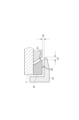
- the inventors considered providing a ground potential frame (anode electrode) so as to cover the peripheral edge of the target as shown in FIG.
- a ground potential frame anode electrode
- the present invention has been made to solve such problems at once, and in a sputtering apparatus that does not use magnetron discharge, it is possible to prevent discharge at the edge of the target while suppressing a decrease in the utilization efficiency of the target.
- the main subject is to make it possible to form a film by
- a sputtering apparatus is a sputtering apparatus for sputtering a target using plasma generated by supplying high-frequency power to an antenna, and is provided around the target and has the same potential as the target. It is characterized by comprising a dummy electrode and an anode electrode having a ground potential, which is provided so as to cover the surface of the dummy electrode facing the same direction as the sputtering surface of the target.
- the dummy electrode having the same potential as the target is provided around the target, and the anode electrode having the ground potential is provided so as to cover the dummy electrode.
- the plasma can be made difficult to spread during this period.
- discharge between the target/dummy electrode and the anode electrode can be prevented, and film formation can be stably performed.
- the surface of the dummy electrode arranged around the target is covered with the anode electrode, it is possible to suppress the deterioration of the utilization efficiency of the target and to suppress the generation of impurities due to the sputtering of the dummy electrode. be done.
- the sputtering surface of the target and the surface of the dummy electrode are formed substantially in the same plane.
- the equipotential surfaces between the target/dummy electrode and the anode electrode can be made nearly flat, so that the occurrence of discharge can be suppressed more effectively.
- the dummy electrode is provided so as to face the side peripheral surface of the target with a gap therebetween.
- arcing that occurs when the electrical contact between the dummy electrode and the side peripheral surfaces of the target is ambiguous can be made less likely to occur.
- a gap is provided between the dummy electrode and the target, a distorted equipotential surface is generated that enters the gap. As a result, this potential surface can cause charged particles to enter the gap, reach the backing plate holding the target, and sputter, thereby creating impurities. Therefore, when a gap is provided between the dummy electrode and the target, it is preferable that the side peripheral surface of the target and the inner peripheral surface of the dummy electrode opposed thereto are inclined with respect to the sputtering surface. In this way, by slanting the gap between the target and the dummy electrode with respect to the sputtering surface, it is possible to reduce the number of charged particles that enter the gap and reach the backing plate at the bottom of the gap.
- the side peripheral surface of the target and the inner peripheral surface of the dummy electrode are inclined to such an extent that the surface of the backing plate cannot be seen from the gap when the sputtering surface is viewed in plan.
- the side peripheral surface of the target and the inner peripheral surface of the dummy electrode form a tapered shape expanding from the sputtering surface toward the back side. In this way, even if the consumption of the target progresses due to sputtering, the possibility that the side surface of the concave consuming portion reaches the target-side peripheral surface is low, and the target can be used continuously up to the vicinity of the bottom surface.
- the dimension of the gap between the target and the dummy electrode is preferably about 0.5 mm or more and about 2.0 mm or less, more preferably about 0.5 mm or more and about 1.0 mm or less.
- the inner peripheral edge of the anode electrode is located near the gap between the target and the dummy electrode when the sputtering surface is viewed in plan. In this way, by arranging the inner peripheral edge of the anode electrode (that is, the tip facing the target from the dummy electrode) near the gap, the charged particles in the vicinity of the gap can be reduced, and the entry of charged particles into the gap can be suppressed. Generation of impurities due to sputtering of the backing plate can be effectively suppressed.
- the equipotential surface created by the applied voltage to the target and the generated plasma changes near the tip of the anode electrode (inner peripheral edge in a side view), when the inner peripheral edge of the anode electrode is placed near the edge of the target, however, depending on the shape of the anode electrode, it may be difficult for ions (such as argon) for sputtering to enter the ends of the target, and the target may not be used effectively. Therefore, it is preferable that the anode electrode tapers from the dummy electrode toward the target. In this way, the change in the equipotential surface at the edge of the target can be smoothed, thereby reducing the change in the ion density at the edge of the target and suppressing the reduction in target utilization rate.
- ions such as argon
- the anode electrode is provided so as to face the surface of the dummy electrode with a gap therebetween, and the facing surfaces of the anode electrode and the dummy electrode are substantially parallel to each other. .
- the equipotential surfaces between the target/dummy electrode and the anode electrode can be brought closer to flatness, so that the occurrence of discharge can be suppressed more effectively.
- the dimension of the gap between the anode electrode and the dummy electrode is 2.0 mm or more and 3.5 mm or less.
- FIG. 2 is a cross-sectional view orthogonal to the longitudinal direction of the antenna schematically showing the configuration of the sputtering apparatus of this embodiment.
- FIG. 2 is a cross-sectional view schematically showing the configuration of the vicinity of the target of the sputtering apparatus of the same embodiment.
- FIG. 4 is a cross-sectional view for explaining a gap between a target, a dummy electrode, and an anode electrode in the same embodiment;
- FIG. 5 is a cross-sectional view schematically showing the configuration of the vicinity of the target of the sputtering apparatus of another embodiment;
- FIG. 2 is a cross-sectional view perpendicular to the longitudinal direction of an antenna schematically showing the configuration of a sputtering apparatus according to another embodiment;
- FIG. 2 is a cross-sectional view schematically showing a configuration in the vicinity of a target devised by the applicant in the course of reaching the present invention;
- the sputtering apparatus 100 of this embodiment is for forming a film on a substrate W by sputtering a target 41 using plasma P generated by supplying high-frequency power to an antenna 6 .
- the substrate W is, for example, a substrate W for a flat panel display (FPD) such as a liquid crystal display or an organic EL display, a flexible substrate W for a flexible display, or the like.
- FPD flat panel display
- the sputtering apparatus 100 includes, as shown in FIG. Then, a bias voltage is applied to the target 41 arranged in the processing chamber S, the target holder 3 holding the target 41, the plurality of linear antennas 6 arranged in the processing chamber S, and the target 41.
- a target bias power supply 5 an antenna 6 for generating plasma P in the processing chamber S, and an antenna power supply 7 for supplying voltage for generating the plasma P to the antenna 6 are provided.
- a high frequency current IR is applied to a plurality of antennas 6 from a high frequency power supply, thereby generating an induced electric field in the processing chamber S and generating inductively coupled plasma P.
- the vacuum container 1 is, for example, a container made of metal, and its interior is evacuated by an evacuation device 8 .
- the vacuum vessel 1 is electrically grounded in this example.
- a sputtering gas or a reactive gas is introduced into the processing chamber S defined by the inner wall of the vacuum vessel 1 via, for example, a flow rate regulator (not shown) and a plurality of gas introduction ports 11 .
- the sputtering gas and the reactive gas may be selected in accordance with the processing to be performed on the substrate W.
- the sputtering gas is, for example, an inert gas such as argon (Ar), and the reactive gas is, for example, oxygen (O 2 ) or nitrogen (N 2 ).
- the substrate holding unit 2 is a holder that holds the flat substrate W in the processing chamber S so that it is horizontal, for example.
- the target holding part 3 adheres and holds a target 41 so as to face the substrate W held by the substrate holding part 2, and is specifically a backing plate.
- the target holder 3 is provided on a side wall 1a (for example, an upper side wall) forming the vacuum vessel 1 .
- An insulating portion 1b having a vacuum sealing function is provided between the target holding portion 3 and the upper wall 1a of the vacuum vessel 1.
- the target holder 3 is water-cooled by a cooling mechanism (not shown), and configured to hold the target 41 and cool it.
- the target 41 has a rectangular plate shape in plan view, and is made of an oxide semiconductor material such as InGaZnO.
- a flat surface of the target 41 facing the substrate W functions as a sputtering surface 41s from which sputtered particles are ejected.
- a target bias power supply 5 that applies a target bias voltage to the target 41 is connected to the target 41 via the target holding unit 3 in this example.
- the target bias voltage is a voltage that draws the ions in the plasma P to the target 41 for sputtering.
- the target bias power supply 5 is configured to apply a constant target bias voltage to the target 41 .
- the target bias power supply 5 is configured so that the voltage applied to the target 41 can be adjusted independently of the voltage applied to the antenna 6 by the antenna power supply 7 .
- the voltage applied to the target 41 by the target bias power supply 5 may be set to a low voltage that attracts the ions in the plasma P to the target 41 for sputtering. do not have.
- a plurality of antennas 6 are arranged in parallel on the same plane along the surface of the substrate W (for example, substantially parallel to the surface of the substrate W) on the surface side of the substrate W in the processing chamber S. .
- the plurality of antennas 6 are arranged at regular intervals so that their longitudinal directions are parallel to each other.
- Each antenna 6 has a linear shape and the same configuration in plan view, and its length is several tens of centimeters or more.
- the antennas 6 of this embodiment are arranged on both sides of each target 41, as shown in FIG. That is, the antennas 6 and targets 41 are alternately arranged, and one target 41 is sandwiched between two antennas 6 .
- the longitudinal direction of each antenna 6 and the longitudinal direction of each target 41 are the same.
- the vicinity of both ends of the antenna 6 respectively penetrates the side walls facing each other of the vacuum vessel 1 .
- each antenna 6 is, for example, copper, aluminum, alloys thereof, stainless steel, etc., but is not limited to these.
- the antenna 6 may be made hollow and a coolant such as cooling water may be flowed therein to cool the antenna 6 .
- each antenna 6 located inside the processing chamber S is covered with a straight tubular insulating cover 51 made of an insulating material. It is not necessary to seal between both ends of the insulating cover 61 and the vacuum vessel 1 . This is because even if gas enters the space inside the insulating cover 61, plasma P is not normally generated in the space because the space is small and electrons travel a short distance.
- the material of the insulating cover 61 is, for example, quartz, alumina, fluororesin, silicon nitride, silicon carbide, silicon, or the like, but is not limited to these.
- Antenna power supply 7 is connected to the feeding end, which is one end of the antenna 6, via a matching circuit 71, and the termination, which is the other end, is directly grounded.
- the antenna power supply 7 applies high frequency power to the antenna 6 via the matching circuit 71 .
- a high-frequency current IR flows through the antenna 6, an induced electric field is generated in the processing chamber S, and an inductively coupled plasma P is generated.
- the high frequency is preferably, for example, 13.56 MHz to 100 MHz, but is not limited to this.
- the antenna power supply 7 is configured so that the voltage applied to the antenna 6 can be adjusted independently of the voltage applied to the target 41 by the target bias power supply 5 .
- the power applied to the antenna 6 by the antenna power supply 7 is sufficient to generate the inductively coupled plasma P in the processing chamber S, and is preferably 5 kW to 100 kW, but is not limited thereto.
- the sputtering apparatus 100 of the present embodiment has a dummy electrode 42 which is equipotential to the target 41 and which is provided around the target 41 .
- An anode electrode 43 at ground potential is provided to cover a substrate-side surface 42s (hereinafter also referred to as a dummy sputtering surface) facing in the same direction as the sputtering surface 41s.
- the dummy electrode 42 has a flat plate shape that is adhered to and held by the target holding portion 3 so as to surround the target 41 in plan view.
- the dummy electrode 42 is connected to the target bias power supply 5 via the target holding unit 3 and has the same potential as the target 41 by applying a constant target bias voltage like the target 41 .
- the plate thickness of the dummy electrode 42 is substantially the same as the plate thickness of the target 41 .
- the dummy sputtering surface 42s of the dummy electrode 42 and the sputtering surface 41s of the target 41 are flat surfaces parallel to each other, and are formed substantially in the same plane (that is, at the same height).
- the dummy electrode 42 is provided such that its inner peripheral surface 42t faces the outer peripheral surface 41t of the target 41 via a gap G1 (hereinafter also referred to as the first gap).
- the dimension D1 of the first gap G1 is substantially constant regardless of the position of the target 41 in the plate thickness direction, and is preferably about 0.5 mm or more and about 2.0 mm or less. more preferred.
- the outer peripheral surface 41t of the target 41 and the inner peripheral surface 42t of the dummy electrode 42 facing each other are formed so as to be inclined with respect to the plane including the sputtering surface 41s.
- the outer peripheral surface 41t of the target 41 and the inner peripheral surface 42t of the dummy electrode 42 are formed to have a tapered shape expanding from the sputtering surface 41s of the target 41 toward the back surface side (target holder 3 side). It is
- the inclination angles of the outer peripheral surface 41t of the target 41 and the inner peripheral surface 42t of the dummy electrode 42 are not particularly limited.
- the inclination angle of each surface is set so that the portion 3 is not exposed. Specifically, as shown in FIG. 3, when the target 41 and the dummy electrode 42 are viewed in cross section, the end portion of the outer peripheral surface 41t of the target 41 on the substrate W side extends in the in-plane direction parallel to the sputtering surface 41s. , the inclination angle of each surface is set so as to be located outside the end portion of the inner peripheral surface 42t of the dummy electrode 42 on the target holding portion 3 side.
- the dummy electrode 42 of this embodiment is made of the same material as the target 41 (an oxide semiconductor material such as InGaZnO).
- the material forming the dummy electrode 42 is not limited to this, and may be made of a metal material such as aluminum or stainless steel. Also, the dummy electrode 42 may be configured by coating a base material made of a metal material with the same material as the target 41 .
- the anode electrode 43 is attached to the upper wall 1a of the vacuum vessel 1 so as to surround the target 41 and the dummy electrode 42, and is electrically grounded.
- the anode electrode 43 has a covering portion 431 formed with a cover surface 43s covering the dummy sputtering surface 42s of the dummy electrode 42 .
- the cover surface 43s has an annular shape that covers the peripheral portion or the entirety of the annular cover surface 43s that surrounds the sputtering surface 41s in a plan view.
- the cover surface 43s is formed so as to face at least the dummy sputtering surface 42s of the dummy electrode 42 via a gap G2 (hereinafter also referred to as a second gap).
- the cover surface 43s is formed substantially parallel to the sputtering surface 41s and the dummy sputtering surface 42s, and the dimension D2 of the second gap G2 is substantially constant regardless of the position in the in-plane direction along the sputtering surface 41s. be.
- a dimension D2 of the second gap G2 is, for example, about 2.0 mm or more and 3.5 mm or less.
- the anode electrode 43 is formed such that its inner peripheral edge 43t is positioned near the first gap G1. is positioned inside the inner peripheral edge of the dummy sputtering surface 42s and outside the outer peripheral edge of the sputtering surface 41s. Viewed from another point of view, in a cross-sectional view as shown in FIG. 3, in the in-plane direction parallel to the sputtering surface 41s, the tip 43t of the covering portion 431 faces inward (direction from the dummy electrode 42 toward the target 41). is positioned in the vicinity of the first gap G1, specifically, positioned inside the inner end of the dummy sputtering surface 42s and outside the outer end of the sputtering surface 41s. ing.
- the covering portion 431 of the anode electrode 43 is formed so as to taper (the plate thickness becomes smaller) from the dummy electrode 42 toward the target 41 .
- an inclined surface 43v that is inclined toward the sputtering surface 41s of the target 41 is formed at the inward tip portion of the rear surface 43u (the surface on the substrate W side) of the cover surface 43s in the covering portion 431 .
- This inclined surface is preferably inclined at an angle of more than 0° and about 30° or less with respect to the sputtering surface 41s, but the angle is not limited to this.
- the thickness of the tip 43t of the covering portion 431 of the anode electrode 43 is preferably about 1 mm or more and about 5 mm or less, but the thickness is not limited to this.
- the dummy electrode 42 having the same potential as the target 41 is provided around the target 41, and the anode electrode 43 having the ground potential is provided so as to cover it. It is possible to reduce the distortion of the electric field between the anode electrode 43 and the dummy electrode 41 and the dummy electrode 43, thereby making it difficult for the plasma P to spread between them. As a result, discharge between the target 41 and the dummy electrode 42 and the anode electrode 43 can be prevented, and film formation can be stably performed.
- the surface of the dummy electrode 42 arranged around the target 41 is covered with the anode electrode 43, it is possible to suppress the deterioration of the utilization efficiency of the target 41, and furthermore, the dummy electrode 42 is sputtered. Generation of impurities is also suppressed.
- the outer peripheral surface 41t of the target 41 and the inner peripheral surface 42t of the dummy electrode 42 are positioned from the sputtering surface 41s of the target 41 toward the rear surface (target holding portion 3). It may be formed to have a tapered shape narrowing toward the side).
- the outer peripheral surface 41t of the target 41 and the inner peripheral surface 42t of the dummy electrode 42 facing each other are inclined with respect to the plane including the sputtering surface 41s, but this is not the only option.
- the outer peripheral surface 41t of the target 41 and the inner peripheral surface 42t of the dummy electrode 42 may not be inclined with respect to the plane containing the sputtering surface 41s. You may form so that it may orthogonally cross.
- the covering portion 431 of the anode electrode 43 is formed so as to taper from the dummy electrode 42 toward the target 41, but this is not restrictive. In another embodiment, the covering portion 431 of the anode electrode 43 may have a certain thickness.
- the sputtering apparatus 100 of the above embodiment is a so-called six-type internal antenna in which the antenna 6 is arranged in the processing chamber S, but the present invention is not limited to this.
- the sputtering apparatus 100 of another embodiment may be of a so-called external antenna 6 type in which the antenna 6 is arranged outside the processing chamber S.
- FIG. 5 For example, in the sputtering apparatus 100, as shown in FIG. 5, a magnetic field transmission window 9 is formed in the side wall (for example, the upper side wall) 1a of the vacuum chamber 1 for transmitting the high frequency magnetic field generated from the antenna 6 into the processing chamber S.
- the antenna 6 may be arranged outside the processing chamber S so as to face the magnetic field transmission window 9 .
- the magnetic field transmission window 9 has a rectangular shape when viewed from the antenna 6 side, and may be formed so that its longitudinal direction is the same as the longitudinal direction of each target 41 .
- the magnetic field transmission window 9 may be composed of a dielectric plate provided so as to cover an opening formed in the side wall 1a of the vacuum vessel 1.
- Materials constituting the dielectric plate may be known materials such as ceramics such as alumina, silicon carbide, and silicon nitride, inorganic materials such as quartz glass and alkali-free glass, and resin materials such as fluororesin (e.g., Teflon). .
- the sputtering apparatus 100 that does not use magnetron discharge, it is possible to prevent discharge at the edge of the target and stably form a film while suppressing a decrease in the utilization efficiency of the target.
Landscapes
- Chemical & Material Sciences (AREA)
- Engineering & Computer Science (AREA)
- Physics & Mathematics (AREA)
- Plasma & Fusion (AREA)
- Analytical Chemistry (AREA)
- Chemical Kinetics & Catalysis (AREA)
- Materials Engineering (AREA)
- Mechanical Engineering (AREA)
- Metallurgy (AREA)
- Organic Chemistry (AREA)
- Physical Vapour Deposition (AREA)
Priority Applications (5)
| Application Number | Priority Date | Filing Date | Title |
|---|---|---|---|
| JP2023567343A JP7653594B2 (ja) | 2021-12-14 | 2021-12-14 | スパッタリング装置 |
| CN202180104037.7A CN118251754A (zh) | 2021-12-14 | 2021-12-14 | 溅镀装置 |
| KR1020247019907A KR20240101688A (ko) | 2021-12-14 | 2021-12-14 | 스퍼터링 장치 |
| PCT/JP2021/046079 WO2023112155A1 (ja) | 2021-12-14 | 2021-12-14 | スパッタリング装置 |
| TW111106280A TWI833166B (zh) | 2021-12-14 | 2022-02-22 | 濺鍍裝置 |
Applications Claiming Priority (1)
| Application Number | Priority Date | Filing Date | Title |
|---|---|---|---|
| PCT/JP2021/046079 WO2023112155A1 (ja) | 2021-12-14 | 2021-12-14 | スパッタリング装置 |
Publications (1)
| Publication Number | Publication Date |
|---|---|
| WO2023112155A1 true WO2023112155A1 (ja) | 2023-06-22 |
Family
ID=86773738
Family Applications (1)
| Application Number | Title | Priority Date | Filing Date |
|---|---|---|---|
| PCT/JP2021/046079 Ceased WO2023112155A1 (ja) | 2021-12-14 | 2021-12-14 | スパッタリング装置 |
Country Status (5)
| Country | Link |
|---|---|
| JP (1) | JP7653594B2 (https=) |
| KR (1) | KR20240101688A (https=) |
| CN (1) | CN118251754A (https=) |
| TW (1) | TWI833166B (https=) |
| WO (1) | WO2023112155A1 (https=) |
Citations (5)
| Publication number | Priority date | Publication date | Assignee | Title |
|---|---|---|---|---|
| JPS5537868U (https=) * | 1978-09-05 | 1980-03-11 | ||
| JPS63243269A (ja) * | 1987-03-30 | 1988-10-11 | Toshiba Corp | スパツタリング・タ−ゲツトの固定装置 |
| JPH03115659U (https=) * | 1990-03-05 | 1991-11-29 | ||
| WO2016006155A1 (ja) * | 2014-07-09 | 2016-01-14 | 株式会社アルバック | 絶縁物ターゲット |
| JP2019052345A (ja) * | 2017-09-14 | 2019-04-04 | 株式会社Screenホールディングス | 成膜方法および成膜装置 |
Family Cites Families (1)
| Publication number | Priority date | Publication date | Assignee | Title |
|---|---|---|---|---|
| JP2021080533A (ja) | 2019-11-21 | 2021-05-27 | 日新電機株式会社 | スパッタリング装置 |
-
2021
- 2021-12-14 CN CN202180104037.7A patent/CN118251754A/zh active Pending
- 2021-12-14 WO PCT/JP2021/046079 patent/WO2023112155A1/ja not_active Ceased
- 2021-12-14 JP JP2023567343A patent/JP7653594B2/ja active Active
- 2021-12-14 KR KR1020247019907A patent/KR20240101688A/ko active Pending
-
2022
- 2022-02-22 TW TW111106280A patent/TWI833166B/zh active
Patent Citations (5)
| Publication number | Priority date | Publication date | Assignee | Title |
|---|---|---|---|---|
| JPS5537868U (https=) * | 1978-09-05 | 1980-03-11 | ||
| JPS63243269A (ja) * | 1987-03-30 | 1988-10-11 | Toshiba Corp | スパツタリング・タ−ゲツトの固定装置 |
| JPH03115659U (https=) * | 1990-03-05 | 1991-11-29 | ||
| WO2016006155A1 (ja) * | 2014-07-09 | 2016-01-14 | 株式会社アルバック | 絶縁物ターゲット |
| JP2019052345A (ja) * | 2017-09-14 | 2019-04-04 | 株式会社Screenホールディングス | 成膜方法および成膜装置 |
Also Published As
| Publication number | Publication date |
|---|---|
| JP7653594B2 (ja) | 2025-03-31 |
| CN118251754A (zh) | 2024-06-25 |
| KR20240101688A (ko) | 2024-07-02 |
| JPWO2023112155A1 (https=) | 2023-06-22 |
| TWI833166B (zh) | 2024-02-21 |
| TW202330969A (zh) | 2023-08-01 |
Similar Documents
| Publication | Publication Date | Title |
|---|---|---|
| JP5567005B2 (ja) | 回転可能なターゲットを備えたマイクロ波を援用したpvd | |
| CN110382734B (zh) | 溅射装置 | |
| JPWO2009142016A1 (ja) | プラズマ生成装置およびプラズマ処理装置 | |
| CN110709533B (zh) | 溅射装置 | |
| SE521904C2 (sv) | Anordning för hybridplasmabehandling | |
| KR100501777B1 (ko) | 플라즈마 처리 장치 | |
| US20080180030A1 (en) | Plasma processing apparatus | |
| JP5969856B2 (ja) | スパッタリング装置 | |
| JP2017033788A (ja) | プラズマ処理装置 | |
| WO2011058608A1 (ja) | プラズマ処理装置 | |
| JP6468521B2 (ja) | 誘導結合型アンテナユニット及びプラズマ処理装置 | |
| JP2018101463A5 (https=) | ||
| EP0326531A2 (en) | Improved RF plasma processing apparatus | |
| WO2021182638A1 (ja) | スパッタリング装置 | |
| JP7653594B2 (ja) | スパッタリング装置 | |
| JP2009191340A (ja) | 成膜装置及び成膜方法 | |
| JP7644332B2 (ja) | スパッタリング装置及び成膜方法 | |
| JP2007027086A (ja) | 誘導結合型プラズマ処理装置 | |
| JP2018154861A (ja) | スパッタリング装置 | |
| JP7727174B2 (ja) | スパッタリング装置 | |
| JP4672436B2 (ja) | プラズマ処理装置 | |
| TWI839097B (zh) | 濺鍍裝置 | |
| JP2015157993A (ja) | スパッタリング装置 | |
| JPH08124864A (ja) | 真空プラズマ処理装置 | |
| US20130126094A1 (en) | Substrate processing apparatus |
Legal Events
| Date | Code | Title | Description |
|---|---|---|---|
| 121 | Ep: the epo has been informed by wipo that ep was designated in this application |
Ref document number: 21968072 Country of ref document: EP Kind code of ref document: A1 |
|
| WWE | Wipo information: entry into national phase |
Ref document number: 2023567343 Country of ref document: JP |
|
| WWE | Wipo information: entry into national phase |
Ref document number: 202180104037.7 Country of ref document: CN |
|
| WWE | Wipo information: entry into national phase |
Ref document number: 202417043178 Country of ref document: IN |
|
| WWE | Wipo information: entry into national phase |
Ref document number: 1020247019907 Country of ref document: KR |
|
| NENP | Non-entry into the national phase |
Ref country code: DE |
|
| 122 | Ep: pct application non-entry in european phase |
Ref document number: 21968072 Country of ref document: EP Kind code of ref document: A1 |