WO2023106055A1 - 伸縮性デバイス - Google Patents
伸縮性デバイス Download PDFInfo
- Publication number
- WO2023106055A1 WO2023106055A1 PCT/JP2022/042512 JP2022042512W WO2023106055A1 WO 2023106055 A1 WO2023106055 A1 WO 2023106055A1 JP 2022042512 W JP2022042512 W JP 2022042512W WO 2023106055 A1 WO2023106055 A1 WO 2023106055A1
- Authority
- WO
- WIPO (PCT)
- Prior art keywords
- conductive member
- stretchable
- insulating layer
- contact
- wiring
- Prior art date
- Legal status (The legal status is an assumption and is not a legal conclusion. Google has not performed a legal analysis and makes no representation as to the accuracy of the status listed.)
- Ceased
Links
Images






Classifications
-
- H—ELECTRICITY
- H05—ELECTRIC TECHNIQUES NOT OTHERWISE PROVIDED FOR
- H05K—PRINTED CIRCUITS; CASINGS OR CONSTRUCTIONAL DETAILS OF ELECTRIC APPARATUS; MANUFACTURE OF ASSEMBLAGES OF ELECTRICAL COMPONENTS
- H05K1/00—Printed circuits
- H05K1/02—Details
- H05K1/0277—Bendability or stretchability details
- H05K1/0283—Stretchable printed circuits
-
- H—ELECTRICITY
- H05—ELECTRIC TECHNIQUES NOT OTHERWISE PROVIDED FOR
- H05K—PRINTED CIRCUITS; CASINGS OR CONSTRUCTIONAL DETAILS OF ELECTRIC APPARATUS; MANUFACTURE OF ASSEMBLAGES OF ELECTRICAL COMPONENTS
- H05K1/00—Printed circuits
- H05K1/02—Details
- H05K1/09—Use of materials for the conductive, e.g. metallic pattern
- H05K1/092—Dispersed materials, e.g. conductive pastes or inks
- H05K1/095—Dispersed materials, e.g. conductive pastes or inks for polymer thick films, i.e. having a permanent organic polymeric binder
-
- H—ELECTRICITY
- H05—ELECTRIC TECHNIQUES NOT OTHERWISE PROVIDED FOR
- H05K—PRINTED CIRCUITS; CASINGS OR CONSTRUCTIONAL DETAILS OF ELECTRIC APPARATUS; MANUFACTURE OF ASSEMBLAGES OF ELECTRICAL COMPONENTS
- H05K1/00—Printed circuits
- H05K1/02—Details
- H05K1/11—Printed elements for providing electric connections to or between printed circuits
- H05K1/111—Pads for surface mounting, e.g. lay-out
-
- H—ELECTRICITY
- H05—ELECTRIC TECHNIQUES NOT OTHERWISE PROVIDED FOR
- H05K—PRINTED CIRCUITS; CASINGS OR CONSTRUCTIONAL DETAILS OF ELECTRIC APPARATUS; MANUFACTURE OF ASSEMBLAGES OF ELECTRICAL COMPONENTS
- H05K1/00—Printed circuits
- H05K1/18—Printed circuits structurally associated with non-printed electric components
- H05K1/181—Printed circuits structurally associated with non-printed electric components associated with surface mounted components
-
- H—ELECTRICITY
- H05—ELECTRIC TECHNIQUES NOT OTHERWISE PROVIDED FOR
- H05K—PRINTED CIRCUITS; CASINGS OR CONSTRUCTIONAL DETAILS OF ELECTRIC APPARATUS; MANUFACTURE OF ASSEMBLAGES OF ELECTRICAL COMPONENTS
- H05K2201/00—Indexing scheme relating to printed circuits covered by H05K1/00
- H05K2201/01—Dielectrics
- H05K2201/0104—Properties and characteristics in general
- H05K2201/0133—Elastomeric or compliant polymer
-
- H—ELECTRICITY
- H05—ELECTRIC TECHNIQUES NOT OTHERWISE PROVIDED FOR
- H05K—PRINTED CIRCUITS; CASINGS OR CONSTRUCTIONAL DETAILS OF ELECTRIC APPARATUS; MANUFACTURE OF ASSEMBLAGES OF ELECTRICAL COMPONENTS
- H05K2201/00—Indexing scheme relating to printed circuits covered by H05K1/00
- H05K2201/03—Conductive materials
- H05K2201/0302—Properties and characteristics in general
- H05K2201/0314—Elastomeric connector or conductor, e.g. rubber with metallic filler
-
- H—ELECTRICITY
- H05—ELECTRIC TECHNIQUES NOT OTHERWISE PROVIDED FOR
- H05K—PRINTED CIRCUITS; CASINGS OR CONSTRUCTIONAL DETAILS OF ELECTRIC APPARATUS; MANUFACTURE OF ASSEMBLAGES OF ELECTRICAL COMPONENTS
- H05K2201/00—Indexing scheme relating to printed circuits covered by H05K1/00
- H05K2201/09—Shape and layout
- H05K2201/09818—Shape or layout details not covered by a single group of H05K2201/09009 - H05K2201/09809
- H05K2201/099—Coating over pads, e.g. solder resist partly over pads
-
- H—ELECTRICITY
- H05—ELECTRIC TECHNIQUES NOT OTHERWISE PROVIDED FOR
- H05K—PRINTED CIRCUITS; CASINGS OR CONSTRUCTIONAL DETAILS OF ELECTRIC APPARATUS; MANUFACTURE OF ASSEMBLAGES OF ELECTRICAL COMPONENTS
- H05K3/00—Apparatus or processes for manufacturing printed circuits
- H05K3/22—Secondary treatment of printed circuits
- H05K3/28—Applying non-metallic protective coatings
- H05K3/284—Applying non-metallic protective coatings for encapsulating mounted components
Definitions
- the present invention relates to stretchable devices.
- Patent Literature 1 describes an elastic device in which a conductive member with high wettability is provided on wiring, and an electronic component is mounted on the conductive member via solder.
- an object of the present invention is to provide a stretchable device capable of suppressing solder leaching of wiring.
- a stretchable substrate stretchable wiring provided on the stretchable substrate, a conductive member in contact with the stretchable wiring, and on the conductive member a solder member provided and in contact with the conductive member; an electronic component electrically connected to the conductive member via the solder member; and a first insulating layer covering at least a portion of the wiring;
- the stretchable device is provided, wherein the outer surface of the end of the wiring that contacts the conductive member is in contact with the conductive member and the first insulating layer that is continuous with the conductive member.
- solder erosion of wiring can be suppressed.
- FIG. 1 is a partial top view of the stretchable device according to the first embodiment.
- FIG. 2A is an enlarged perspective view of the elastic wiring.
- FIG. 2B is an enlarged perspective view of the elastic wiring.
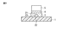
- FIG. 3 is a sectional view taken along line III--III in FIG.
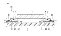
- FIG. 4 is a sectional view taken along line IV--IV of FIG.
- FIG. 5 is a partial cross-sectional view of an elastic device according to a first modified example of the first embodiment.
- FIG. 6 is a partial cross-sectional view of an elastic device according to a second modification of the first embodiment.
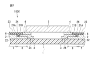
- FIG. 7 is a partial cross-sectional view of an elastic device according to a third modified example of the first embodiment.
- FIG. 1 is a partial top view of the stretchable device according to the first embodiment.
- FIG. 2A is an enlarged perspective view of the elastic wiring.
- FIG. 2B is an enlarged perspective view of the elastic wiring.
- FIG. 3 is a sectional view taken along
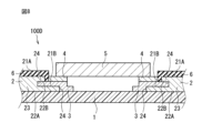
- FIG. 8 is a partial cross-sectional view of an elastic device according to a fourth modified example of the first embodiment.
- FIG. 9 is a partial cross-sectional view of an elastic device according to a fifth modification of the first embodiment.
- FIG. 10 is a partial cross-sectional view of the stretchable device according to the second embodiment.
- FIG. 11 is a partial cross-sectional view of an elastic device according to a fourth embodiment.
- FIG. 1 is a partial top view of the stretchable device according to the first embodiment.
- 2A and 2B are enlarged perspective views of elastic wiring.
- FIG. 3 is a sectional view taken along line III--III in FIG.
- FIG. 4 is a sectional view taken along line IV--IV of FIG.
- the first insulating layer 6 has a multi-step structure, and in FIG. 1, straight lines indicate the stepped portions.
- the stretchable device 100 has stretchable wiring 2 laid on a stretchable base material 1 and electronic components 5 mounted thereon.
- FIG. 1 is a partially enlarged top view of an area where an electronic component 5 is mounted.
- the shape of the stretchable device 100 is not particularly limited, and may be rectangular or circular when viewed from the thickness direction of the stretchable base material 1 .
- the arrangement of the elastic wiring 2 is not particularly limited.
- the longitudinal direction of the stretchable base material 1 is indicated by a double arrow X. As shown in FIG. In this embodiment, the direction in which the stretchable device 100 stretches matches the longitudinal direction of the stretchable base material 1, but it does not have to match.
- the stretchable device 100 includes a stretchable substrate 1, stretchable wiring 2 provided on the stretchable substrate 1, a conductive member 3 in contact with the stretchable wiring 2, and a conductive member 3 provided on the stretchable member 3. a solder member 4 in contact with the conductive member 3; an electronic component 5 electrically connected to the conductive member 3 via the solder member 4; And prepare.
- stretchable wiring 2 is provided on stretchable substrate 1 . Further, as shown in FIG. 4, the conductive member 3 is in contact with the upper surface 21 and the end surface 24 of the elastic wiring 2 .
- the stretchable base material 1 is a sheet-like or film-like stretchable base material, and is made of, for example, a stretchable resin material.
- the resin material include thermoplastic polyurethane and the like.
- the thickness of the elastic base material 1 is not particularly limited, but from the viewpoint of not inhibiting the expansion and contraction of the surface of the living body when attached to the living body, it is preferably 1 mm or less, more preferably 100 ⁇ m or less, and more preferably 50 ⁇ m. More preferably: Moreover, the thickness of the stretchable base material 1 is preferably 1 ⁇ m or more.
- the stretchable wiring 2 refers to the stretchable wiring 2 that is routed in a predetermined pattern on the main surface of the stretchable base material 1 and that is directly connected to the electronic component 5 . That is, the stretchable device 100 may have wiring that is not connected to the electronic component 5 .
- the stretchable wiring 2 contains conductive particles and resin.
- a mixture of metal powder such as Ag, Cu, and Ni as conductive particles and elastomeric resin such as silicone resin can be used.
- the average particle size of the conductive particles is not particularly limited, it is preferably 0.01 ⁇ m or more and 10 ⁇ m or less.
- the shape of the conductive particles is preferably spherical.
- the thickness of the elastic wiring 2 is not particularly limited, it is preferably 100 ⁇ m or less, more preferably 50 ⁇ m or less. Moreover, it is preferable that the thickness of the elastic wiring 2 is 0.01 ⁇ m or more.
- the line width of the elastic wiring 2 is not particularly limited, it is preferably 0.1 ⁇ m or more, and more preferably 10 mm or less. Further, the number of elastic wirings 2 included in the elastic wirings 2 is not particularly limited.
- the conductive member 3 it is preferable to use a material that is less susceptible to solder erosion than the elastic wiring 2.
- the conductive member 3 preferably contains a thermosetting resin.
- the conductive member 3 containing a thermosetting resin include a compound of a metal filler and a resin containing a thermosetting resin.
- metal fillers include silver fillers, copper fillers, and nickel fillers. Since the conductive member 3 contains the thermosetting resin in this way, it is possible to suppress solder erosion due to reaction between the elastic wiring 2 and the solder member 4 .
- the conductive member 3 may be made of metal foil, metal plating, or the like.
- the solder member 4 is not particularly limited, it preferably contains tin and bismuth as metal components, and is preferably so-called low-temperature solder. By using low-temperature solder, even if the elastic substrate 1, the elastic wiring 2, and the electronic component 5 have low heat resistance temperatures, the electronic component 5 can be soldered without damaging them.
- the electronic component 5 is not particularly limited, examples thereof include amplifiers (operational amplifiers, transistors, etc.), diodes, integrated circuits (ICs), capacitors, resistors, inductors, and the like.
- the first insulating layer 6 is preferably made of a resin material or a mixture of a resin material and an inorganic material. Rubber, vinyl chloride, ester-based, amide-based elastomer resins, epoxy, phenol, acrylic, polyester, imide-based, rosin, cellulose, polyethylene terephthalate-based, polyethylene naphthalate-based, and polycarbonate-based resins can be used.
- the outer surface of the end of the stretchable wiring 2 that contacts the conductive member 3 is in contact with the conductive member 3 and the first insulating layer 6 that is continuous with the conductive member 3 .
- the outer surface refers to the surface of the elastic wiring 2 excluding the surface on the base material side.
- the surface of the elastic wire 2 is composed of an upper surface 21, a lower surface 22, a side surface 23 and an end surface 24.
- the lower surface refers to the surface closest to the stretchable substrate 1
- the upper surface refers to the surface facing the lower surface.
- the elastic wiring 2 is not limited to a rectangular parallelepiped shape as shown in FIG. 2A, and may have a curved surface or unevenness. Similarly, each surface may not be rectangular and may have rounded corners.
- the elastic wiring 2 may have a multistage structure as shown in FIG. 2B.
- a multi-stage structure a plurality of upper surfaces 21 and lower surfaces 22 are present.
- the top surface closest to the electronic component 5 in the thickness direction of the elastic base material 1 is the top surface 21A
- the top surface second closest to the electronic component is the second top surface 21B.
- the elastic wiring 2 may have a third upper surface, and the number of upper surfaces is not particularly limited.
- the lower surface closest to the elastic substrate 1 in the thickness direction of the elastic substrate 1 is the lowest surface 22A, and the second closest lower surface is the second lower surface 22B.
- the elastic wiring 2 may have a third lower surface, and the number of lower surfaces is not particularly limited.
- the surface closest to the substrate 1 is the lowermost surface 22A. That is, the second lower surface 22B is included in the outer surface, but the lowermost surface 22A is not included in the outer surface. Similarly, even if the elastic wiring 2 has a third lower surface or a fourth lower surface, they are not included in the outer surface.
- the upper surface 21 and the lower surface 22 do not have to match the actual top and bottom. It is a name for convenience of description, and the lower surface may be arranged above the upper surface when the stretchable device 100 is used. In addition, the lower surface 22 and the stretchable base material 1 may not be in contact with each other. As will be described later, an insulating layer or thin film may be arranged between the lower surface 22 and the elastic base material 1 .
- the side surface 23 and the end surface 24 connect the upper surface 21 and the lower surface 22 .
- the elastic wire 2 has two side surfaces 23 and two end surfaces, but illustration of one of the two end surfaces is omitted in FIGS. 2A and 2B.
- the end surface of the stretchable wiring 2 that contacts the conductive member 3 is designated as 24 .
- the outer surface of the elastic wiring 2 as a whole is composed of the upper surface 21, the side surfaces 23, and both end surfaces. 24.
- the end of the stretchable wiring 2 on the side that contacts the conductive member 3 is the farthest end from the end face 24 (end A ), more preferably 0.5 mm in addition to the end A, and more preferably 1 mm in addition to the end A. With such a structure, contact between the elastic wiring 2 and the solder member 4 can be more reliably suppressed.
- each surface of each component other than the elastic wiring 2 is also determined in the same manner.
- the upper surface 21 of the elastic wiring 2 is omitted and described as the upper surface 21 .
- Each surface of the elastic wiring 2 is referred to when each surface is labeled with a code. The surfaces of other components will be explained without omitting descriptions and without reference numerals.
- the outer surface of the elastic wiring 2 is covered with the conductive member 3 and the first insulating layer 6 . That is, since it becomes difficult for the elastic wiring 2 and the solder member 4 to come into contact with each other, solder erosion can be suppressed and the reliability of the 100 can be improved.
- the first insulating layer 6 is continuous with the conductive member 3 .
- the first insulating layer 6 and the conductive member 3 are in contact. If the first insulating layer 6 and the conductive member 3 are not in contact with each other, the solder member 4 is provided on the elastic wiring 2 from the surface of the conductive member 3 to the both end faces of the conductive member 3. There is a risk of contact with the elastic wiring 2 via the end face where Since the first insulating layer 6 and the conductive member 3 are continuous, it is possible to suppress the occurrence of solder erosion.
- the conductive member 3 and the first insulating layer 6 being continuous may mean that only the end surface of the conductive member 3 and the end surface of the first insulating layer 6 are in contact.
- Layer 6 preferably overlaps the ends of conductive member 3 .
- Wetting and spreading of the solder member 4 is stopped at the contact point with the first insulating layer 6 . That is, by adopting such a structure, it is possible to suppress the solder member 4 from wetting and spreading.
- the first insulating layer 6 and the solder member 4 may be in contact with each other, or may not be in contact with each other as shown in FIG.
- the connection performance between the conductive member 3 and the elastic wiring 2 can be improved.
- the elastic device 100 expands and contracts in the extending direction of the elastic wiring 2, it is conceivable that the elastic wiring 2 and the conductive member 3 are separated from each other due to the difference in the amount of expansion and contraction.
- the connection performance between the elastic wiring 2 and the conductive member 3 can be increased, and peeling can be suppressed.
- the length of the elastic wiring 2 in the width direction is smaller than the length of the conductive member 3 in the same direction.
- the contact area between the elastic wiring 2 and the conductive member 3 is large. That is, as shown in FIGS. 3 and 4, it is preferable that the conductive member 3 is in contact with the upper surface 21, both side surfaces 23 and end surfaces 24 of the wiring. In addition, the entire conductive member 3 may be provided on the elastic wiring 2 .
- the solder member 4 is in contact with the upper surface of the conductive member 3.
- the solder member 4 may be in contact with the conductive member 3 other than the upper surface thereof.
- the conductive member 3 when viewed from the thickness direction of the stretchable base material 1 , the conductive member 3 may be in contact with the end surface or both side surfaces of the conductive member 3 that do not overlap with the stretchable wiring 2 .
- it may be in contact with the stretchable base material 1 .
- the shape is not particularly limited. For example, it may have a fillet.
- solder member 4 Since the solder member 4 is wet and spreads, it is difficult to control the area accurately. That is, as described above, when the solder member 4 is arranged so as to be in contact with the surface of the conductive member 3 overlapping the elastic wiring 2 when viewed from the thickness direction of the elastic base material 1, the solder member 4 is unintentionally wet. By spreading, there is a possibility that the elastic wiring 2 and the solder member 4 may come into contact with each other, resulting in solder erosion.
- the electronic component 5 is electrically connected to the conductive member 3 and the elastic wiring 2 via the solder member 4.
- the electronic component 5 is electrically connected to the two elastic wires 2 as shown in FIGS. good too.
- the first insulating layer 6 covers at least part of the elastic wiring 2
- the size is not particularly limited, but it preferably covers the entire elastic wiring 2 .
- the entire stretchable wiring 2 as shown in FIG. may
- the outer surface of the end of the elastic wiring 2 on the side contacting the conductive member 3 is in contact with the conductive member 3 and the first insulating layer 6 .
- the outer surfaces of the elastic wire 2 are the top surface 21 , the side surfaces 23 , and the end surfaces 24 in contact with the conductive member 3 .
- the length of the elastic wiring 2 in the width direction is smaller than the length of the conductive member 3 in the same direction, so the conductive member 3 and the side surfaces 23 are in contact with each other.
- the conductive member 3 does not need to be in contact with the entire side surfaces 23, and may not be partially in contact with them.
- the solder member 4 spreads through the end surface of the conductive member 3 that contacts the stretchable base material 1, the solder member 4 and the end surface 24 do not come into contact with each other. It should be noted that the conductive member 3 need not be in contact with the entire end face 24, and may be in contact only partially.
- the upper surface 21 is in contact with the conductive member 3 and the first insulating layer 6 continuous with the conductive member 3 .
- contact between the solder member 4 and the elastic wiring 2 via the end surface provided on the elastic wiring 2 among both end surfaces of the conductive member 3 is suppressed. can. That is, by adopting the above configuration, contact between the solder member 4 and the stretchable wiring 2 via both side surfaces and both end surfaces of the conductive member 3 can be suppressed, and the reliability of the stretchable device 100 can be improved. .
- the first insulating layer 6 is preferably in contact with the end of the conductive member 3 .
- the first insulating layer 6 is preferably in contact with one end surface, both side surfaces and the upper surface of the conductive member 3 .
- the elastic device 100 expands and contracts during use, there is a risk of peeling occurring at the interface of each constituent element.
- the first insulating layer 6 is provided on the conductive member 3, the first insulating layer 6, the conductive member 3 and the stretchable wiring 2 overlap each other when viewed from the thickness direction of the substrate. With such an arrangement, the upward movement of the conductive member 3 can be suppressed by the first insulating layer 6 . Therefore, vertical peeling of the interface between the upper surface 21 and the conductive member 3 can be reduced.
- each component is not limited to that shown in FIG. Although the thickness of the first insulating layer 6 is larger than the thickness of the elastic wiring 2 in FIG. 4, the opposite may be true. Further, the thickness of the portion of the first insulating layer 6 provided on the elastic wiring 2 and the thickness of the portion provided on the conductive member 3 may be the same or different. good. The thickness of the portion of the conductive member 3 provided on the stretchable wiring 2 and the thickness of the portion provided on the stretchable substrate 1 may be the same or different.
- FIG. 5 is a partial cross-sectional view of an elastic device 100A according to a first modified example of the first embodiment.
- the stretchable device 100A differs from the stretchable device 100 according to the first embodiment in the arrangement of the conductive members 3 and the solder members 4 .
- part of the first insulating layer 6 is in contact with both the conductive member 3 and the solder member 4 .
- solder leaching may occur.
- the conductive member 3 and the solder member 4 come into contact with each other, the conductive member 3 may also be eroded. The larger the contact area between the conductive member 3 and the solder member 4, the more likely the conductive member 3 will be leached.
- connection performance of the solder member 4 is greatly affected by the contact area with other members. That is, if the contact area of the solder member 4 is small, the interface of the solder member 4 may break during expansion and contraction, increasing the risk of defects. That is, it is preferable to increase the contact area of the solder member 4 without increasing the contact area between the conductive member 3 and the solder member 4 .
- Solder erosion of the conductive member 3 is suppressed by increasing the connection area between the solder member 4 and a member in which solder erosion is unlikely to occur. It is possible to suppress breakage of the interface of the member 4 .
- the contact area between the first insulating layer 6 and the solder member 4, in which solder leaching is less likely to occur, is increased.
- the first insulating layer 6, the conductive member 3, and the solder member 4 overlap each other in plan view.
- the portion described above also overlaps with the elastic wiring 2 in a plan view. That is, it is possible to further reduce the possibility that the elastic wiring 2 and the conductive member 3 are vertically broken.
- the solder member 4 is in contact with the first insulating layer 6 in the extending direction of the wiring.
- the conductive member 3 is less stretchable than the stretchable wiring 2, such as when the conductive member 3 contains a thermosetting resin, increasing the area of the conductive member 3 in a plan view will increase the stretchable device 100A. elasticity is greatly reduced.
- the area of the conductive member 3 is reduced, the area of connection with the solder member 4 is also reduced, resulting in deterioration of connection performance. Since the solder member 4 is in contact with the first insulating layer 6 in the wiring extending direction, the connection area between the solder member 4 and the conductive member 3 can be increased, and the connection performance can be improved.
- solder member 4 overlaps the conductive member 3 in plan view.
- the contact area of the solder member 4 is increased because not only the end surface of the insulating layer but also a portion of the upper surface is in contact with the solder member 4 . That is, peeling of the solder member 4 can be suppressed, and the contact area between the solder member 4 and the conductive member 3 can be increased.
- a part of the solder member 4 may be arranged between the conductive member 3 and the first insulating layer 6 .
- the thickness of the first insulating layer 6 arranged between the conductive member 3 and the solder member 4 is not particularly limited. The thickness may be the same as or different from the thickness of the first insulating layer 6 provided on the elastic wiring 2 .
- FIG. 6 is a partial cross-sectional view of an elastic device 100B according to a second modification of the first embodiment.
- the stretchable device 100B differs from the stretchable device 100 according to the first embodiment in the arrangement of the stretchable wirings 2 and the conductive members 3 .
- the elastic device 100B and part of the elastic wiring 2 are arranged on the conductive member 3, and the part of the elastic wiring 2 and the solder member 4 in the longitudinal direction of the elastic base material 1 are arranged.
- a first insulating layer 6 is arranged therebetween.
- the first insulating layer 6 is arranged between the elastic wiring 2 and the solder member 4 in order to suppress contact between the two. preferably.
- the first insulating layer 6 can suppress solder erosion of the elastic wiring 2 .
- the thickness of the conductive member 3 can be made uniform while increasing the contact area between the elastic wiring 2 and the conductive member 3 .
- the electronic component 5 overlaps the elastic base material 1, the conductive member 3, and the solder member 4 in plan view. That is, the flatness of the electronic component 5 is determined by these three members. If the flatness of the electronic component 5 is impaired, the reliability of the component is reduced. That is, by adopting such a structure, it is possible to increase the contact area between the stretchable wiring 2 and the conductive member 3 while suppressing deterioration in the reliability of the component.
- the shape of the first insulating layer 6 is not particularly limited. As shown in FIG. 6, by making the thickness constant, the shape may be adjusted to the unevenness of the conductive member 3. Alternatively, the thickness may be changed for printing. By doing so, the height of the upper surface may be matched.
- FIG. 7 is a partial cross-sectional view of an elastic device 100C according to a third modified example of the first embodiment.
- the stretchable device 100C differs in the first insulating layer 6 from the stretchable device 100 according to the first embodiment.
- a part of the elastic wiring 2 is arranged under the conductive member 3 in the elastic device 100C.
- the upper surface 21 and the end surface 24 come into contact with the elastic wiring 2 . That is, it is possible to increase the contact area between the stretchable wiring 2 and the conductive member 3 and suppress breakage during stretching.
- the elastic wiring 2 includes a first portion 7 having a large thickness and a second portion 8 having a thickness smaller than that of the first portion 7, and at least a part of the second portion 8 is arranged under the conductive member 3. preferably.
- the upper surface 21 and the end surface 24 can be arranged so as to be in contact with the conductive member 3 .
- the shortest distance from the elastic substrate 1 differs between the portion of the conductive member 3 overlapping the elastic wiring 2 and the portion not overlapping the elastic wiring 2 by the thickness of the second portion 8 . That is, if the thickness of the second portion 8 is large, the unevenness of the conductive member 3 becomes large, and the flatness is impaired.
- the contact area between the elastic wiring 2 and the conductive member 3 is increased, Loss of flatness of the conductive member 3 can be suppressed. Also, the height of the area where the electronic component 5 is mounted can be reduced.
- the length of the second portion 8 is not particularly limited. A part of the second portion 8 may be arranged under the conductive member 3 as shown in FIG. 7, or the entire second portion 8 may be arranged under the conductive member 3. .
- FIG. 8 is a partial cross-sectional view of an elastic device 100D according to a fourth modified example of the first embodiment.
- the stretchable device 100D differs from the stretchable device 100 according to the first embodiment in the arrangement of the stretchable wiring 2 and the first insulating layer 6.
- FIG. 8 is a partial cross-sectional view of an elastic device 100D according to a fourth modified example of the first embodiment.
- the stretchable device 100D differs from the stretchable device 100 according to the first embodiment in the arrangement of the stretchable wiring 2 and the first insulating layer 6.
- a part of the elastic wiring 2 preferably contacts the upper surface and the lower surface of the conductive member 3 respectively.
- the elastic wiring 2 is divided into two branches and the conductive member 3 is arranged between them.
- the structure shown in FIG. 8 can be obtained by printing the elastic wiring 2 once, printing the conductive member 3 so as to partially overlap it, and then printing the elastic wiring 2 again.
- the printing method described above is merely an example, and a different manufacturing method may be used.
- the elastic wiring 2 is in contact with one end surface, top surface, and bottom surface of the conductive member 3 . That is, the contact area is increased, and the reliability at the time of connection is increased.
- the elastic wiring 2 in contact with the upper surface of the conductive member 3 can suppress separation between the conductive member 3 and the elastic wiring 2 in contact with the lower surface of the conductive member 3. .
- the elastic wiring 2 in contact with the lower surface of the conductive member 3 can suppress peeling of the elastic wiring 2 in contact with the upper surface of the conductive member 3 and the conductive member 3 .
- the elastic wirings 2 above and below the conductive member 3 the deformation of the conductive member 3 can be suppressed.
- the elastic wiring 2 since the elastic wiring 2 is in contact with the upper and lower surfaces of the conductive member 3, even if one of the contact portions is peeled off, the other contact portion can ensure electrical connection. can.
- the thickness of the portion in contact with the upper surface of the conductive member 3 and the portion in contact with the lower surface of the elastic wiring 2 may be the same or may be different. Also, the length is not particularly limited, and as shown in FIG. , may be the same, or the portion in contact with the top surface may be longer.
- a first insulating layer 6 is arranged between a part of the elastic wiring 2 and the solder member 4 in the longitudinal direction of the elastic base material 1 .
- FIG. 9 is a partial cross-sectional view of an elastic device 100E according to a fifth modification of the first embodiment.
- the stretchable device 100E differs from the stretchable device 100 according to the first embodiment in that it includes a second insulating layer 9 .
- the second insulating layer 9 is preferably made of a resin material or a mixture of a resin material and an inorganic material. Rubber, vinyl chloride, ester-based, amide-based elastomer resins, epoxy, phenol, acrylic, polyester, imide-based, rosin, cellulose, polyethylene terephthalate-based, polyethylene naphthalate-based, and polycarbonate-based resins can be used. It may be the same material as the first insulating layer 6 or a different material.
- a second insulating layer 9 is further provided, and the second insulating layer 9 is in contact with the end of the conductive member 3 opposite to the side that contacts the first insulating layer 6 .
- the first insulating layer 6 it is preferable to provide the first insulating layer 6 so as to overlap with the conductive member 3 in order to suppress separation between the conductive member 3 and the upper surface 21 .
- the second insulating layer 9 can suppress peeling of the conductive member 3 and the end surface 24 .
- the second insulating layer 9 is arranged at the end of the conductive member 3 that overlaps the electronic component 5 in plan view.
- part of the second insulating layer 9 is preferably provided on the end of the conductive member 3 , and part of the second insulating layer 9 is arranged between the solder member 4 and the conductive member 3 . It is more preferable that As with the first insulating layer 6 , peeling can be suppressed by increasing the connection area with the conductive member 3 or the solder member 4 . Moreover, it is preferable that the second insulating layer 9 is in contact with the solder member 4 in the extending direction of the wiring. As with the first insulating layer 6, the area between the solder member 4 and the conductive member 3 can be maximized.
- the second insulating layer 9 is provided on the end portion of the conductive member 3 , it is possible to suppress the movement of the conductive member 3 toward the electronic component 5 . That is, it is possible to suppress separation between the stretchable base material 1 and the conductive member 3 .
- the second insulating layer 9 is on the side in contact with the first insulating layer 6 with reference to the conductive member 3 in contact with one of the elastic wirings 2. preferably contact the opposite end and the end opposite to the side contacting the first insulating layer 6 with reference to the conductive member 3 contacting the other elastic wiring 2 .
- a plurality of conductive members 3 are provided in contact with each of the plurality of elastic wirings 2 , and the second insulating layer 9 is in contact with the plurality of conductive members 3 .
- the other conductive member 3 can suppress the separation.
- the other conductive member 3 and the first insulating layer 6 are separated in the longitudinal direction of the stretchable base material 1
- the one conductive member 3 and the first insulating layer 6 suppress separation.
- the contact portion that may peel in the longitudinal direction of the stretchable base material 1 is not limited to the conductive member 3 and the first insulating layer 6 .
- the longitudinal direction of the stretchable base material 1 where peeling easily occurs that is, the stretching direction has been described
- the direction in which the stretchable base material 1 is separated and opposed is not particularly limited.
- the number of elastic wires 2 connected to the electronic component 5 is not particularly limited.
- FIG. 10 is a partial cross-sectional view of an elastic device 101 according to the second embodiment.
- the stretchable device 101 differs from the stretchable device 100 according to the first embodiment in that it includes a protective layer 10 .
- the protective layer 10 is a layer for protecting the elastic wiring 2 from moisture.
- the elastic wiring 2 absorbs moisture, ion migration occurs, and there is a risk of short-circuiting due to energization with wiring having a different potential.
- ion migration of the elastic wiring 2 can be suppressed.
- the protective layer 10 is preferably a resin material or a mixture of a resin material and an inorganic material.
- the resin material include urethane, styrene, olefin, silicone, fluorine, nitrile rubber, latex rubber, Elastomer-based resins such as vinyl chloride, ester-based, and amide-based resins, epoxy, phenol, acrylic, polyester, imide-based, rosin, cellulose, polyethylene terephthalate-based, polyethylene naphthalate-based, and polycarbonate-based resins can be used.
- the same material as the first insulating layer 6 and the second insulating layer 9 may be used, or a different material may be used.
- the protective layer 10 From the viewpoint of water absorption as the protective layer 10, it is preferable to select a member having a high water absorption rate for the protective layer 10.
- the members covering the outer surface of the elastic wiring 2 are the same except for the conductive member 3. Formation during printing is facilitated, and the risk of defective occurrence can be reduced.
- the protective layer 10 may be arranged integrally so as to be in contact with the lower surfaces 22 of the plurality of elastic wirings 2, or each elastic wiring 2 may be separated from each other. may be placed as Moreover, it is preferable that a protective layer 10 is arranged between the conductive member 3 and the stretchable base material 1 . It is possible to increase the contact area of the conductive member 3 and suppress breakage.
- FIG. 11 is a partial cross-sectional view of the stretchable device 102 according to the third embodiment.
- the stretchable device 102 differs from the stretchable device 100 according to the first embodiment in that it includes a resin layer 11 .
- a resin layer 11 is further provided to cover the electronic component 5 as shown in FIG.
- the resin layer 11 can protect the electronic component 5 from external forces.
- Materials for the resin layer 11 include polyvinyl chloride, polyethylene, polystyrene, polycarbonate, polyvinylidene fluoride, polyimide, liquid crystal polymer, polytetrafluoroethylene, phenol resin, epoxy resin, urethane resin, acrylic resin, and silicone resin. , elastomer resins such as styrene/butadiene resins, and the like.
- the stretchable device 100 shrinks as the resin contained in the resin layer 11 hardens. In other words, there is a risk that the interface between the constituent elements of the stretchable device 100 will peel off during contraction.
- peeling due to shrinkage during resin effect can be suppressed. The same applies to other peeling suppression effects.
- the resin layer 11 preferably overlaps the entire solder member 4, and more preferably overlaps the entire conductive member 3 and the solder member 4 in plan view.
- the surface 12 of the resin layer 11 is preferably in contact with the conductive member 3
- more preferably the surface 12 of the resin layer 11 is in contact with the first insulating layer 6 .
- FIG. 11 shows the contact portion between the surface 12 of the resin layer 11 and the first insulating layer 6 as a contact 13 .
- the resin layer 11 has a role of protecting the electronic component 5 from external force, so it is inferior to the stretchable wiring 2 in stretchability. Therefore, the amount of expansion and contraction greatly changes at the interface between the portion that overlaps with the resin layer 11 and the portion that does not overlap with the resin layer 11 in plan view. Since stress tends to concentrate in a portion where the amount of expansion and contraction changes greatly, breakage is likely to occur. More specifically, if the solder member 4 is partially overlapped with the resin layer 11 and partially not overlapped with the resin layer 11 in plan view, the solder member 4 may break. The same applies to the conductive member 3 as well.
- the solder member 4 is included inside the resin layer. That is, since the amount of expansion and contraction of the solder member 4 as a whole approaches uniformity, breakage of the solder member 4 can be suppressed. The same applies to the conductive member 3 as well.
- the first insulating layer 6 covers the conductive member 3 in each of the embodiments and modifications described above.
- the present invention is not limited to the structure described above, and the conductive member 3 and the first insulating layer 6 only need to be continuous. Specifically, the end face of the conductive member 3 and the first insulating layer 6 do not have to be in contact with each other and not overlap in plan view.
- stretchable device which concerns on one Embodiment of this invention is as follows. ⁇ 1> a stretchable base material; a stretchable wiring provided on the stretchable substrate; a conductive member in contact with the elastic wiring; a solder member provided on the conductive member and in contact with the conductive member; an electronic component electrically connected to the conductive member via the solder member; a first insulating layer covering at least part of the elastic wiring,
- ⁇ 2> The stretchable device according to ⁇ 1>, wherein the first insulating layer is in contact with the end of the conductive member.
- ⁇ 3> The stretchable device according to ⁇ 1> or ⁇ 2>, wherein the first insulating layer overlaps the end portion of the conductive member in plan view.
- ⁇ 4> The stretchable device according to ⁇ 3>, wherein a portion of the first insulating layer is in contact with both the conductive member and the solder member.
- ⁇ 5> The stretchable device according to any one of ⁇ 1> to ⁇ 4>, wherein the first insulating layer, the conductive member, and the solder member overlap each other in plan view.
- ⁇ 6> The stretchable device according to ⁇ 5>, wherein a portion of the first insulating layer is arranged between the solder member and the conductive member. ⁇ 7> ⁇ 1> to ⁇ 6>, wherein a portion of the elastic wiring is disposed on the conductive member, and the first insulating layer is disposed between a portion of the elastic wiring and the solder member.
- the stretchable device according to any one of . ⁇ 8> The stretchable device according to any one of ⁇ 1> to ⁇ 7>, wherein a part of the stretchable wiring is arranged under the conductive member.
- the elastic wiring comprises a first portion having a greater thickness and a second portion having a thickness less than the first portion, at least a portion of the second portion being disposed under the conductive member, ⁇ 1
- the stretchable device according to any one of > to ⁇ 8>.
- ⁇ 10> The stretchable device according to any one of ⁇ 1> to ⁇ 9>, wherein a part of the stretchable wiring contacts the upper surface and the lower surface of the conductive member, respectively.
- ⁇ 11> further comprising a second insulating layer; ⁇ 10> according to any one of ⁇ 1> to ⁇ 10>, wherein the second insulating layer is in contact with the end of the conductive member opposite to the side in contact with the first insulating layer. stretchable device.
- ⁇ 12> The stretchable device according to ⁇ 11>, wherein a part of the two insulating layers is arranged on the opposite end of the conductive member.
- ⁇ 13> comprising two elastic wires facing each other and separated from each other;
- the second insulating layer is in contact with an end opposite to the side in contact with the first insulating layer with respect to the conductive member in contact with one of the elastic wires, and with the other elastic wire.
- the stretchable device according to ⁇ 11> or ⁇ 12> which is in contact with the end opposite to the side in contact with the first insulating layer with respect to the conductive member.
- ⁇ 14> It has an additional protective layer, The stretchable device according to any one of ⁇ 1> to ⁇ 13>, wherein the protective layer is arranged between the stretchable wiring and the stretchable base material.
- the protective layer is arranged between the stretchable wiring and the stretchable base material.
- the conductive member contains a thermosetting resin.
- a stretchable device according to an embodiment of the present invention can be used with electronic components mounted.
Landscapes
- Engineering & Computer Science (AREA)
- Microelectronics & Electronic Packaging (AREA)
- Structure Of Printed Boards (AREA)
Priority Applications (4)
| Application Number | Priority Date | Filing Date | Title |
|---|---|---|---|
| JP2023566195A JP7658459B2 (ja) | 2021-12-08 | 2022-11-16 | 伸縮性デバイス |
| CN202280080738.6A CN118355735A (zh) | 2021-12-08 | 2022-11-16 | 伸缩性器件 |
| EP22903986.2A EP4412403A4 (en) | 2021-12-08 | 2022-11-16 | EXPANDABLE DEVICE |
| US18/734,081 US20240324099A1 (en) | 2021-12-08 | 2024-06-05 | Stretchable device |
Applications Claiming Priority (2)
| Application Number | Priority Date | Filing Date | Title |
|---|---|---|---|
| JP2021-199233 | 2021-12-08 | ||
| JP2021199233 | 2021-12-08 |
Related Child Applications (1)
| Application Number | Title | Priority Date | Filing Date |
|---|---|---|---|
| US18/734,081 Continuation US20240324099A1 (en) | 2021-12-08 | 2024-06-05 | Stretchable device |
Publications (1)
| Publication Number | Publication Date |
|---|---|
| WO2023106055A1 true WO2023106055A1 (ja) | 2023-06-15 |
Family
ID=86730404
Family Applications (1)
| Application Number | Title | Priority Date | Filing Date |
|---|---|---|---|
| PCT/JP2022/042512 Ceased WO2023106055A1 (ja) | 2021-12-08 | 2022-11-16 | 伸縮性デバイス |
Country Status (5)
| Country | Link |
|---|---|
| US (1) | US20240324099A1 (https=) |
| EP (1) | EP4412403A4 (https=) |
| JP (1) | JP7658459B2 (https=) |
| CN (1) | CN118355735A (https=) |
| WO (1) | WO2023106055A1 (https=) |
Cited By (2)
| Publication number | Priority date | Publication date | Assignee | Title |
|---|---|---|---|---|
| WO2025249078A1 (ja) * | 2024-05-27 | 2025-12-04 | 株式会社村田製作所 | 伸縮性デバイス |
| WO2026048693A1 (ja) * | 2024-08-27 | 2026-03-05 | 株式会社村田製作所 | 伸縮性デバイス |
Citations (4)
| Publication number | Priority date | Publication date | Assignee | Title |
|---|---|---|---|---|
| WO2009081929A1 (ja) * | 2007-12-26 | 2009-07-02 | Fujikura Ltd. | 実装基板及びその製造方法 |
| JP2016143763A (ja) * | 2015-02-02 | 2016-08-08 | 株式会社フジクラ | 伸縮性回路基板 |
| WO2020203135A1 (ja) * | 2019-03-29 | 2020-10-08 | 株式会社村田製作所 | 伸縮性実装基板 |
| WO2021235282A1 (ja) * | 2020-05-21 | 2021-11-25 | 株式会社村田製作所 | 伸縮性配線基板 |
Family Cites Families (2)
| Publication number | Priority date | Publication date | Assignee | Title |
|---|---|---|---|---|
| JP6903981B2 (ja) * | 2017-03-23 | 2021-07-14 | セイコーエプソン株式会社 | 検出装置 |
| US20210076496A1 (en) * | 2019-09-09 | 2021-03-11 | Flex Ltd. | Solder electronic components to printed conductive ink |
-
2022
- 2022-11-16 EP EP22903986.2A patent/EP4412403A4/en active Pending
- 2022-11-16 CN CN202280080738.6A patent/CN118355735A/zh active Pending
- 2022-11-16 WO PCT/JP2022/042512 patent/WO2023106055A1/ja not_active Ceased
- 2022-11-16 JP JP2023566195A patent/JP7658459B2/ja active Active
-
2024
- 2024-06-05 US US18/734,081 patent/US20240324099A1/en active Pending
Patent Citations (5)
| Publication number | Priority date | Publication date | Assignee | Title |
|---|---|---|---|---|
| WO2009081929A1 (ja) * | 2007-12-26 | 2009-07-02 | Fujikura Ltd. | 実装基板及びその製造方法 |
| JP2016143763A (ja) * | 2015-02-02 | 2016-08-08 | 株式会社フジクラ | 伸縮性回路基板 |
| JP6518451B2 (ja) | 2015-02-02 | 2019-05-22 | 株式会社フジクラ | 伸縮性回路基板 |
| WO2020203135A1 (ja) * | 2019-03-29 | 2020-10-08 | 株式会社村田製作所 | 伸縮性実装基板 |
| WO2021235282A1 (ja) * | 2020-05-21 | 2021-11-25 | 株式会社村田製作所 | 伸縮性配線基板 |
Non-Patent Citations (1)
| Title |
|---|
| See also references of EP4412403A4 |
Cited By (2)
| Publication number | Priority date | Publication date | Assignee | Title |
|---|---|---|---|---|
| WO2025249078A1 (ja) * | 2024-05-27 | 2025-12-04 | 株式会社村田製作所 | 伸縮性デバイス |
| WO2026048693A1 (ja) * | 2024-08-27 | 2026-03-05 | 株式会社村田製作所 | 伸縮性デバイス |
Also Published As
| Publication number | Publication date |
|---|---|
| EP4412403A1 (en) | 2024-08-07 |
| CN118355735A (zh) | 2024-07-16 |
| US20240324099A1 (en) | 2024-09-26 |
| EP4412403A4 (en) | 2025-10-01 |
| JPWO2023106055A1 (https=) | 2023-06-15 |
| JP7658459B2 (ja) | 2025-04-08 |
Similar Documents
| Publication | Publication Date | Title |
|---|---|---|
| JP6518451B2 (ja) | 伸縮性回路基板 | |
| US10083887B2 (en) | Chip component-embedded resin multilayer substrate and manufacturing method thereof | |
| US20240324099A1 (en) | Stretchable device | |
| KR102103792B1 (ko) | 회로 기판의 접속 구조 | |
| US10531569B2 (en) | Printed circuit board and method of fabricating the same | |
| TWI497535B (zh) | 具有軟性材料層之微電阻元件及其製造方法 | |
| TWI699147B (zh) | 軟性電路板及包括其的電子裝置 | |
| KR20150018247A (ko) | 전자기기의 접합구조 | |
| CN112423472B (zh) | 软硬结合电路板及其制作方法 | |
| KR101846853B1 (ko) | 더미를 이용하여 강성 조절되는 연성 반도체 기판 | |
| CN107958875B (zh) | 半导体装置以及布线基板的设计方法 | |
| US20240422919A1 (en) | Stretchable device | |
| JP7718604B2 (ja) | 伸縮性デバイス | |
| TWI782100B (zh) | 貫通電極基板及使用有貫通電極基板之半導體裝置 | |
| JP5006162B2 (ja) | 電気接続部材 | |
| WO2000049652A1 (en) | Bonding material, semiconductor device, method of manufacturing semiconductor device, circuit board and electronic device | |
| JP7794361B2 (ja) | 伸縮性デバイス | |
| KR101896225B1 (ko) | 회로 기판 및 이의 제조 방법 | |
| US20250203765A1 (en) | Stretchable device | |
| KR20160046977A (ko) | 이방성 도전입자 | |
| WO2017006665A1 (ja) | 基板およびこれを備える電子機器 | |
| JP2010165852A (ja) | 積層型半導体装置 | |
| JP2014183086A (ja) | 積層型配線板 | |
| CN120129140A (zh) | 柔性印刷电路板、包括其的电子设备及柔性印刷电路板的制造方法 | |
| JP2015026773A (ja) | 配線基板 |
Legal Events
| Date | Code | Title | Description |
|---|---|---|---|
| 121 | Ep: the epo has been informed by wipo that ep was designated in this application |
Ref document number: 22903986 Country of ref document: EP Kind code of ref document: A1 |
|
| ENP | Entry into the national phase |
Ref document number: 2023566195 Country of ref document: JP Kind code of ref document: A |
|
| ENP | Entry into the national phase |
Ref document number: 2022903986 Country of ref document: EP Effective date: 20240430 |
|
| WWE | Wipo information: entry into national phase |
Ref document number: 202280080738.6 Country of ref document: CN |
|
| NENP | Non-entry into the national phase |
Ref country code: DE |