WO2023106055A1 - 伸縮性デバイス - Google Patents
伸縮性デバイス Download PDFInfo
- Publication number
- WO2023106055A1 WO2023106055A1 PCT/JP2022/042512 JP2022042512W WO2023106055A1 WO 2023106055 A1 WO2023106055 A1 WO 2023106055A1 JP 2022042512 W JP2022042512 W JP 2022042512W WO 2023106055 A1 WO2023106055 A1 WO 2023106055A1
- Authority
- WO
- WIPO (PCT)
- Prior art keywords
- conductive member
- stretchable
- insulating layer
- contact
- wiring
- Prior art date
Links
Images


Classifications
-
- H—ELECTRICITY
- H05—ELECTRIC TECHNIQUES NOT OTHERWISE PROVIDED FOR
- H05K—PRINTED CIRCUITS; CASINGS OR CONSTRUCTIONAL DETAILS OF ELECTRIC APPARATUS; MANUFACTURE OF ASSEMBLAGES OF ELECTRICAL COMPONENTS
- H05K1/00—Printed circuits
- H05K1/02—Details
-
- H—ELECTRICITY
- H05—ELECTRIC TECHNIQUES NOT OTHERWISE PROVIDED FOR
- H05K—PRINTED CIRCUITS; CASINGS OR CONSTRUCTIONAL DETAILS OF ELECTRIC APPARATUS; MANUFACTURE OF ASSEMBLAGES OF ELECTRICAL COMPONENTS
- H05K1/00—Printed circuits
- H05K1/02—Details
- H05K1/09—Use of materials for the conductive, e.g. metallic pattern
-
- H—ELECTRICITY
- H05—ELECTRIC TECHNIQUES NOT OTHERWISE PROVIDED FOR
- H05K—PRINTED CIRCUITS; CASINGS OR CONSTRUCTIONAL DETAILS OF ELECTRIC APPARATUS; MANUFACTURE OF ASSEMBLAGES OF ELECTRICAL COMPONENTS
- H05K3/00—Apparatus or processes for manufacturing printed circuits
- H05K3/30—Assembling printed circuits with electric components, e.g. with resistor
- H05K3/32—Assembling printed circuits with electric components, e.g. with resistor electrically connecting electric components or wires to printed circuits
Definitions
- the present invention relates to stretchable devices.
- Patent Literature 1 describes an elastic device in which a conductive member with high wettability is provided on wiring, and an electronic component is mounted on the conductive member via solder.
- an object of the present invention is to provide a stretchable device capable of suppressing solder leaching of wiring.
- a stretchable substrate stretchable wiring provided on the stretchable substrate, a conductive member in contact with the stretchable wiring, and on the conductive member a solder member provided and in contact with the conductive member; an electronic component electrically connected to the conductive member via the solder member; and a first insulating layer covering at least a portion of the wiring;
- the stretchable device is provided, wherein the outer surface of the end of the wiring that contacts the conductive member is in contact with the conductive member and the first insulating layer that is continuous with the conductive member.
- solder erosion of wiring can be suppressed.
- FIG. 1 is a partial top view of the stretchable device according to the first embodiment.
- FIG. 2A is an enlarged perspective view of the elastic wiring.
- FIG. 2B is an enlarged perspective view of the elastic wiring.
- FIG. 3 is a sectional view taken along line III--III in FIG.
- FIG. 4 is a sectional view taken along line IV--IV of FIG.
- FIG. 5 is a partial cross-sectional view of an elastic device according to a first modified example of the first embodiment.
- FIG. 6 is a partial cross-sectional view of an elastic device according to a second modification of the first embodiment.
- FIG. 7 is a partial cross-sectional view of an elastic device according to a third modified example of the first embodiment.
- FIG. 1 is a partial top view of the stretchable device according to the first embodiment.
- FIG. 2A is an enlarged perspective view of the elastic wiring.
- FIG. 2B is an enlarged perspective view of the elastic wiring.
- FIG. 3 is a sectional view taken along
- FIG. 8 is a partial cross-sectional view of an elastic device according to a fourth modified example of the first embodiment.
- FIG. 9 is a partial cross-sectional view of an elastic device according to a fifth modification of the first embodiment.
- FIG. 10 is a partial cross-sectional view of the stretchable device according to the second embodiment.
- FIG. 11 is a partial cross-sectional view of an elastic device according to a fourth embodiment.
- FIG. 1 is a partial top view of the stretchable device according to the first embodiment.
- 2A and 2B are enlarged perspective views of elastic wiring.
- FIG. 3 is a sectional view taken along line III--III in FIG.
- FIG. 4 is a sectional view taken along line IV--IV of FIG.
- the first insulating layer 6 has a multi-step structure, and in FIG. 1, straight lines indicate the stepped portions.
- the stretchable device 100 has stretchable wiring 2 laid on a stretchable base material 1 and electronic components 5 mounted thereon.
- FIG. 1 is a partially enlarged top view of an area where an electronic component 5 is mounted.
- the shape of the stretchable device 100 is not particularly limited, and may be rectangular or circular when viewed from the thickness direction of the stretchable base material 1 .
- the arrangement of the elastic wiring 2 is not particularly limited.
- the longitudinal direction of the stretchable base material 1 is indicated by a double arrow X. As shown in FIG. In this embodiment, the direction in which the stretchable device 100 stretches matches the longitudinal direction of the stretchable base material 1, but it does not have to match.
- the stretchable device 100 includes a stretchable substrate 1, stretchable wiring 2 provided on the stretchable substrate 1, a conductive member 3 in contact with the stretchable wiring 2, and a conductive member 3 provided on the stretchable member 3. a solder member 4 in contact with the conductive member 3; an electronic component 5 electrically connected to the conductive member 3 via the solder member 4; And prepare.
- stretchable wiring 2 is provided on stretchable substrate 1 . Further, as shown in FIG. 4, the conductive member 3 is in contact with the upper surface 21 and the end surface 24 of the elastic wiring 2 .
- the stretchable base material 1 is a sheet-like or film-like stretchable base material, and is made of, for example, a stretchable resin material.
- the resin material include thermoplastic polyurethane and the like.
- the thickness of the elastic base material 1 is not particularly limited, but from the viewpoint of not inhibiting the expansion and contraction of the surface of the living body when attached to the living body, it is preferably 1 mm or less, more preferably 100 ⁇ m or less, and more preferably 50 ⁇ m. More preferably: Moreover, the thickness of the stretchable base material 1 is preferably 1 ⁇ m or more.
- the stretchable wiring 2 refers to the stretchable wiring 2 that is routed in a predetermined pattern on the main surface of the stretchable base material 1 and that is directly connected to the electronic component 5 . That is, the stretchable device 100 may have wiring that is not connected to the electronic component 5 .
- the stretchable wiring 2 contains conductive particles and resin.
- a mixture of metal powder such as Ag, Cu, and Ni as conductive particles and elastomeric resin such as silicone resin can be used.
- the average particle size of the conductive particles is not particularly limited, it is preferably 0.01 ⁇ m or more and 10 ⁇ m or less.
- the shape of the conductive particles is preferably spherical.
- the thickness of the elastic wiring 2 is not particularly limited, it is preferably 100 ⁇ m or less, more preferably 50 ⁇ m or less. Moreover, it is preferable that the thickness of the elastic wiring 2 is 0.01 ⁇ m or more.
- the line width of the elastic wiring 2 is not particularly limited, it is preferably 0.1 ⁇ m or more, and more preferably 10 mm or less. Further, the number of elastic wirings 2 included in the elastic wirings 2 is not particularly limited.
- the conductive member 3 it is preferable to use a material that is less susceptible to solder erosion than the elastic wiring 2.
- the conductive member 3 preferably contains a thermosetting resin.
- the conductive member 3 containing a thermosetting resin include a compound of a metal filler and a resin containing a thermosetting resin.
- metal fillers include silver fillers, copper fillers, and nickel fillers. Since the conductive member 3 contains the thermosetting resin in this way, it is possible to suppress solder erosion due to reaction between the elastic wiring 2 and the solder member 4 .
- the conductive member 3 may be made of metal foil, metal plating, or the like.
- the solder member 4 is not particularly limited, it preferably contains tin and bismuth as metal components, and is preferably so-called low-temperature solder. By using low-temperature solder, even if the elastic substrate 1, the elastic wiring 2, and the electronic component 5 have low heat resistance temperatures, the electronic component 5 can be soldered without damaging them.
- the electronic component 5 is not particularly limited, examples thereof include amplifiers (operational amplifiers, transistors, etc.), diodes, integrated circuits (ICs), capacitors, resistors, inductors, and the like.
- the first insulating layer 6 is preferably made of a resin material or a mixture of a resin material and an inorganic material. Rubber, vinyl chloride, ester-based, amide-based elastomer resins, epoxy, phenol, acrylic, polyester, imide-based, rosin, cellulose, polyethylene terephthalate-based, polyethylene naphthalate-based, and polycarbonate-based resins can be used.
- the outer surface of the end of the stretchable wiring 2 that contacts the conductive member 3 is in contact with the conductive member 3 and the first insulating layer 6 that is continuous with the conductive member 3 .
- the outer surface refers to the surface of the elastic wiring 2 excluding the surface on the base material side.
- the surface of the elastic wire 2 is composed of an upper surface 21, a lower surface 22, a side surface 23 and an end surface 24.
- the lower surface refers to the surface closest to the stretchable substrate 1
- the upper surface refers to the surface facing the lower surface.
- the elastic wiring 2 is not limited to a rectangular parallelepiped shape as shown in FIG. 2A, and may have a curved surface or unevenness. Similarly, each surface may not be rectangular and may have rounded corners.
- the elastic wiring 2 may have a multistage structure as shown in FIG. 2B.
- a multi-stage structure a plurality of upper surfaces 21 and lower surfaces 22 are present.
- the top surface closest to the electronic component 5 in the thickness direction of the elastic base material 1 is the top surface 21A
- the top surface second closest to the electronic component is the second top surface 21B.
- the elastic wiring 2 may have a third upper surface, and the number of upper surfaces is not particularly limited.
- the lower surface closest to the elastic substrate 1 in the thickness direction of the elastic substrate 1 is the lowest surface 22A, and the second closest lower surface is the second lower surface 22B.
- the elastic wiring 2 may have a third lower surface, and the number of lower surfaces is not particularly limited.
- the surface closest to the substrate 1 is the lowermost surface 22A. That is, the second lower surface 22B is included in the outer surface, but the lowermost surface 22A is not included in the outer surface. Similarly, even if the elastic wiring 2 has a third lower surface or a fourth lower surface, they are not included in the outer surface.
- the upper surface 21 and the lower surface 22 do not have to match the actual top and bottom. It is a name for convenience of description, and the lower surface may be arranged above the upper surface when the stretchable device 100 is used. In addition, the lower surface 22 and the stretchable base material 1 may not be in contact with each other. As will be described later, an insulating layer or thin film may be arranged between the lower surface 22 and the elastic base material 1 .
- the side surface 23 and the end surface 24 connect the upper surface 21 and the lower surface 22 .
- the elastic wire 2 has two side surfaces 23 and two end surfaces, but illustration of one of the two end surfaces is omitted in FIGS. 2A and 2B.
- the end surface of the stretchable wiring 2 that contacts the conductive member 3 is designated as 24 .
- the outer surface of the elastic wiring 2 as a whole is composed of the upper surface 21, the side surfaces 23, and both end surfaces. 24.
- the end of the stretchable wiring 2 on the side that contacts the conductive member 3 is the farthest end from the end face 24 (end A ), more preferably 0.5 mm in addition to the end A, and more preferably 1 mm in addition to the end A. With such a structure, contact between the elastic wiring 2 and the solder member 4 can be more reliably suppressed.
- each surface of each component other than the elastic wiring 2 is also determined in the same manner.
- the upper surface 21 of the elastic wiring 2 is omitted and described as the upper surface 21 .
- Each surface of the elastic wiring 2 is referred to when each surface is labeled with a code. The surfaces of other components will be explained without omitting descriptions and without reference numerals.
- the outer surface of the elastic wiring 2 is covered with the conductive member 3 and the first insulating layer 6 . That is, since it becomes difficult for the elastic wiring 2 and the solder member 4 to come into contact with each other, solder erosion can be suppressed and the reliability of the 100 can be improved.
- the first insulating layer 6 is continuous with the conductive member 3 .
- the first insulating layer 6 and the conductive member 3 are in contact. If the first insulating layer 6 and the conductive member 3 are not in contact with each other, the solder member 4 is provided on the elastic wiring 2 from the surface of the conductive member 3 to the both end faces of the conductive member 3. There is a risk of contact with the elastic wiring 2 via the end face where Since the first insulating layer 6 and the conductive member 3 are continuous, it is possible to suppress the occurrence of solder erosion.
- the conductive member 3 and the first insulating layer 6 being continuous may mean that only the end surface of the conductive member 3 and the end surface of the first insulating layer 6 are in contact.
- Layer 6 preferably overlaps the ends of conductive member 3 .
- Wetting and spreading of the solder member 4 is stopped at the contact point with the first insulating layer 6 . That is, by adopting such a structure, it is possible to suppress the solder member 4 from wetting and spreading.
- the first insulating layer 6 and the solder member 4 may be in contact with each other, or may not be in contact with each other as shown in FIG.
- the connection performance between the conductive member 3 and the elastic wiring 2 can be improved.
- the elastic device 100 expands and contracts in the extending direction of the elastic wiring 2, it is conceivable that the elastic wiring 2 and the conductive member 3 are separated from each other due to the difference in the amount of expansion and contraction.
- the connection performance between the elastic wiring 2 and the conductive member 3 can be increased, and peeling can be suppressed.
- the length of the elastic wiring 2 in the width direction is smaller than the length of the conductive member 3 in the same direction.
- the contact area between the elastic wiring 2 and the conductive member 3 is large. That is, as shown in FIGS. 3 and 4, it is preferable that the conductive member 3 is in contact with the upper surface 21, both side surfaces 23 and end surfaces 24 of the wiring. In addition, the entire conductive member 3 may be provided on the elastic wiring 2 .
- the solder member 4 is in contact with the upper surface of the conductive member 3.
- the solder member 4 may be in contact with the conductive member 3 other than the upper surface thereof.
- the conductive member 3 when viewed from the thickness direction of the stretchable base material 1 , the conductive member 3 may be in contact with the end surface or both side surfaces of the conductive member 3 that do not overlap with the stretchable wiring 2 .
- it may be in contact with the stretchable base material 1 .
- the shape is not particularly limited. For example, it may have a fillet.
- solder member 4 Since the solder member 4 is wet and spreads, it is difficult to control the area accurately. That is, as described above, when the solder member 4 is arranged so as to be in contact with the surface of the conductive member 3 overlapping the elastic wiring 2 when viewed from the thickness direction of the elastic base material 1, the solder member 4 is unintentionally wet. By spreading, there is a possibility that the elastic wiring 2 and the solder member 4 may come into contact with each other, resulting in solder erosion.
- the electronic component 5 is electrically connected to the conductive member 3 and the elastic wiring 2 via the solder member 4.
- the electronic component 5 is electrically connected to the two elastic wires 2 as shown in FIGS. good too.
- the first insulating layer 6 covers at least part of the elastic wiring 2
- the size is not particularly limited, but it preferably covers the entire elastic wiring 2 .
- the entire stretchable wiring 2 as shown in FIG. may
- the outer surface of the end of the elastic wiring 2 on the side contacting the conductive member 3 is in contact with the conductive member 3 and the first insulating layer 6 .
- the outer surfaces of the elastic wire 2 are the top surface 21 , the side surfaces 23 , and the end surfaces 24 in contact with the conductive member 3 .
- the length of the elastic wiring 2 in the width direction is smaller than the length of the conductive member 3 in the same direction, so the conductive member 3 and the side surfaces 23 are in contact with each other.
- the conductive member 3 does not need to be in contact with the entire side surfaces 23, and may not be partially in contact with them.
- the solder member 4 spreads through the end surface of the conductive member 3 that contacts the stretchable base material 1, the solder member 4 and the end surface 24 do not come into contact with each other. It should be noted that the conductive member 3 need not be in contact with the entire end face 24, and may be in contact only partially.
- the upper surface 21 is in contact with the conductive member 3 and the first insulating layer 6 continuous with the conductive member 3 .
- contact between the solder member 4 and the elastic wiring 2 via the end surface provided on the elastic wiring 2 among both end surfaces of the conductive member 3 is suppressed. can. That is, by adopting the above configuration, contact between the solder member 4 and the stretchable wiring 2 via both side surfaces and both end surfaces of the conductive member 3 can be suppressed, and the reliability of the stretchable device 100 can be improved. .
- the first insulating layer 6 is preferably in contact with the end of the conductive member 3 .
- the first insulating layer 6 is preferably in contact with one end surface, both side surfaces and the upper surface of the conductive member 3 .
- the elastic device 100 expands and contracts during use, there is a risk of peeling occurring at the interface of each constituent element.
- the first insulating layer 6 is provided on the conductive member 3, the first insulating layer 6, the conductive member 3 and the stretchable wiring 2 overlap each other when viewed from the thickness direction of the substrate. With such an arrangement, the upward movement of the conductive member 3 can be suppressed by the first insulating layer 6 . Therefore, vertical peeling of the interface between the upper surface 21 and the conductive member 3 can be reduced.
- each component is not limited to that shown in FIG. Although the thickness of the first insulating layer 6 is larger than the thickness of the elastic wiring 2 in FIG. 4, the opposite may be true. Further, the thickness of the portion of the first insulating layer 6 provided on the elastic wiring 2 and the thickness of the portion provided on the conductive member 3 may be the same or different. good. The thickness of the portion of the conductive member 3 provided on the stretchable wiring 2 and the thickness of the portion provided on the stretchable substrate 1 may be the same or different.
- FIG. 5 is a partial cross-sectional view of an elastic device 100A according to a first modified example of the first embodiment.
- the stretchable device 100A differs from the stretchable device 100 according to the first embodiment in the arrangement of the conductive members 3 and the solder members 4 .
- part of the first insulating layer 6 is in contact with both the conductive member 3 and the solder member 4 .
- solder leaching may occur.
- the conductive member 3 and the solder member 4 come into contact with each other, the conductive member 3 may also be eroded. The larger the contact area between the conductive member 3 and the solder member 4, the more likely the conductive member 3 will be leached.
- connection performance of the solder member 4 is greatly affected by the contact area with other members. That is, if the contact area of the solder member 4 is small, the interface of the solder member 4 may break during expansion and contraction, increasing the risk of defects. That is, it is preferable to increase the contact area of the solder member 4 without increasing the contact area between the conductive member 3 and the solder member 4 .
- Solder erosion of the conductive member 3 is suppressed by increasing the connection area between the solder member 4 and a member in which solder erosion is unlikely to occur. It is possible to suppress breakage of the interface of the member 4 .
- the contact area between the first insulating layer 6 and the solder member 4, in which solder leaching is less likely to occur, is increased.
- the first insulating layer 6, the conductive member 3, and the solder member 4 overlap each other in plan view.
- the portion described above also overlaps with the elastic wiring 2 in a plan view. That is, it is possible to further reduce the possibility that the elastic wiring 2 and the conductive member 3 are vertically broken.
- the solder member 4 is in contact with the first insulating layer 6 in the extending direction of the wiring.
- the conductive member 3 is less stretchable than the stretchable wiring 2, such as when the conductive member 3 contains a thermosetting resin, increasing the area of the conductive member 3 in a plan view will increase the stretchable device 100A. elasticity is greatly reduced.
- the area of the conductive member 3 is reduced, the area of connection with the solder member 4 is also reduced, resulting in deterioration of connection performance. Since the solder member 4 is in contact with the first insulating layer 6 in the wiring extending direction, the connection area between the solder member 4 and the conductive member 3 can be increased, and the connection performance can be improved.
- solder member 4 overlaps the conductive member 3 in plan view.
- the contact area of the solder member 4 is increased because not only the end surface of the insulating layer but also a portion of the upper surface is in contact with the solder member 4 . That is, peeling of the solder member 4 can be suppressed, and the contact area between the solder member 4 and the conductive member 3 can be increased.
- a part of the solder member 4 may be arranged between the conductive member 3 and the first insulating layer 6 .
- the thickness of the first insulating layer 6 arranged between the conductive member 3 and the solder member 4 is not particularly limited. The thickness may be the same as or different from the thickness of the first insulating layer 6 provided on the elastic wiring 2 .
- FIG. 6 is a partial cross-sectional view of an elastic device 100B according to a second modification of the first embodiment.
- the stretchable device 100B differs from the stretchable device 100 according to the first embodiment in the arrangement of the stretchable wirings 2 and the conductive members 3 .
- the elastic device 100B and part of the elastic wiring 2 are arranged on the conductive member 3, and the part of the elastic wiring 2 and the solder member 4 in the longitudinal direction of the elastic base material 1 are arranged.
- a first insulating layer 6 is arranged therebetween.
- the first insulating layer 6 is arranged between the elastic wiring 2 and the solder member 4 in order to suppress contact between the two. preferably.
- the first insulating layer 6 can suppress solder erosion of the elastic wiring 2 .
- the thickness of the conductive member 3 can be made uniform while increasing the contact area between the elastic wiring 2 and the conductive member 3 .
- the electronic component 5 overlaps the elastic base material 1, the conductive member 3, and the solder member 4 in plan view. That is, the flatness of the electronic component 5 is determined by these three members. If the flatness of the electronic component 5 is impaired, the reliability of the component is reduced. That is, by adopting such a structure, it is possible to increase the contact area between the stretchable wiring 2 and the conductive member 3 while suppressing deterioration in the reliability of the component.
- the shape of the first insulating layer 6 is not particularly limited. As shown in FIG. 6, by making the thickness constant, the shape may be adjusted to the unevenness of the conductive member 3. Alternatively, the thickness may be changed for printing. By doing so, the height of the upper surface may be matched.
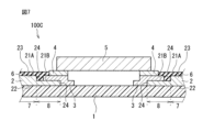
- FIG. 7 is a partial cross-sectional view of an elastic device 100C according to a third modified example of the first embodiment.
- the stretchable device 100C differs in the first insulating layer 6 from the stretchable device 100 according to the first embodiment.
- a part of the elastic wiring 2 is arranged under the conductive member 3 in the elastic device 100C.
- the upper surface 21 and the end surface 24 come into contact with the elastic wiring 2 . That is, it is possible to increase the contact area between the stretchable wiring 2 and the conductive member 3 and suppress breakage during stretching.
- the elastic wiring 2 includes a first portion 7 having a large thickness and a second portion 8 having a thickness smaller than that of the first portion 7, and at least a part of the second portion 8 is arranged under the conductive member 3. preferably.
- the upper surface 21 and the end surface 24 can be arranged so as to be in contact with the conductive member 3 .
- the shortest distance from the elastic substrate 1 differs between the portion of the conductive member 3 overlapping the elastic wiring 2 and the portion not overlapping the elastic wiring 2 by the thickness of the second portion 8 . That is, if the thickness of the second portion 8 is large, the unevenness of the conductive member 3 becomes large, and the flatness is impaired.
- the contact area between the elastic wiring 2 and the conductive member 3 is increased, Loss of flatness of the conductive member 3 can be suppressed. Also, the height of the area where the electronic component 5 is mounted can be reduced.
- the length of the second portion 8 is not particularly limited. A part of the second portion 8 may be arranged under the conductive member 3 as shown in FIG. 7, or the entire second portion 8 may be arranged under the conductive member 3. .
- FIG. 8 is a partial cross-sectional view of an elastic device 100D according to a fourth modified example of the first embodiment.
- the stretchable device 100D differs from the stretchable device 100 according to the first embodiment in the arrangement of the stretchable wiring 2 and the first insulating layer 6.
- a part of the elastic wiring 2 preferably contacts the upper surface and the lower surface of the conductive member 3 respectively.
- the elastic wiring 2 is divided into two branches and the conductive member 3 is arranged between them.
- the structure shown in FIG. 8 can be obtained by printing the elastic wiring 2 once, printing the conductive member 3 so as to partially overlap it, and then printing the elastic wiring 2 again.
- the printing method described above is merely an example, and a different manufacturing method may be used.
- the elastic wiring 2 is in contact with one end surface, top surface, and bottom surface of the conductive member 3 . That is, the contact area is increased, and the reliability at the time of connection is increased.
- the elastic wiring 2 in contact with the upper surface of the conductive member 3 can suppress separation between the conductive member 3 and the elastic wiring 2 in contact with the lower surface of the conductive member 3. .
- the elastic wiring 2 in contact with the lower surface of the conductive member 3 can suppress peeling of the elastic wiring 2 in contact with the upper surface of the conductive member 3 and the conductive member 3 .
- the elastic wirings 2 above and below the conductive member 3 the deformation of the conductive member 3 can be suppressed.
- the elastic wiring 2 since the elastic wiring 2 is in contact with the upper and lower surfaces of the conductive member 3, even if one of the contact portions is peeled off, the other contact portion can ensure electrical connection. can.
- the thickness of the portion in contact with the upper surface of the conductive member 3 and the portion in contact with the lower surface of the elastic wiring 2 may be the same or may be different. Also, the length is not particularly limited, and as shown in FIG. , may be the same, or the portion in contact with the top surface may be longer.
- a first insulating layer 6 is arranged between a part of the elastic wiring 2 and the solder member 4 in the longitudinal direction of the elastic base material 1 .
- FIG. 9 is a partial cross-sectional view of an elastic device 100E according to a fifth modification of the first embodiment.
- the stretchable device 100E differs from the stretchable device 100 according to the first embodiment in that it includes a second insulating layer 9 .
- the second insulating layer 9 is preferably made of a resin material or a mixture of a resin material and an inorganic material. Rubber, vinyl chloride, ester-based, amide-based elastomer resins, epoxy, phenol, acrylic, polyester, imide-based, rosin, cellulose, polyethylene terephthalate-based, polyethylene naphthalate-based, and polycarbonate-based resins can be used. It may be the same material as the first insulating layer 6 or a different material.
- a second insulating layer 9 is further provided, and the second insulating layer 9 is in contact with the end of the conductive member 3 opposite to the side that contacts the first insulating layer 6 .
- the first insulating layer 6 it is preferable to provide the first insulating layer 6 so as to overlap with the conductive member 3 in order to suppress separation between the conductive member 3 and the upper surface 21 .
- the second insulating layer 9 can suppress peeling of the conductive member 3 and the end surface 24 .
- the second insulating layer 9 is arranged at the end of the conductive member 3 that overlaps the electronic component 5 in plan view.
- part of the second insulating layer 9 is preferably provided on the end of the conductive member 3 , and part of the second insulating layer 9 is arranged between the solder member 4 and the conductive member 3 . It is more preferable that As with the first insulating layer 6 , peeling can be suppressed by increasing the connection area with the conductive member 3 or the solder member 4 . Moreover, it is preferable that the second insulating layer 9 is in contact with the solder member 4 in the extending direction of the wiring. As with the first insulating layer 6, the area between the solder member 4 and the conductive member 3 can be maximized.
- the second insulating layer 9 is provided on the end portion of the conductive member 3 , it is possible to suppress the movement of the conductive member 3 toward the electronic component 5 . That is, it is possible to suppress separation between the stretchable base material 1 and the conductive member 3 .
- the second insulating layer 9 is on the side in contact with the first insulating layer 6 with reference to the conductive member 3 in contact with one of the elastic wirings 2. preferably contact the opposite end and the end opposite to the side contacting the first insulating layer 6 with reference to the conductive member 3 contacting the other elastic wiring 2 .
- a plurality of conductive members 3 are provided in contact with each of the plurality of elastic wirings 2 , and the second insulating layer 9 is in contact with the plurality of conductive members 3 .
- the other conductive member 3 can suppress the separation.
- the other conductive member 3 and the first insulating layer 6 are separated in the longitudinal direction of the stretchable base material 1
- the one conductive member 3 and the first insulating layer 6 suppress separation.
- the contact portion that may peel in the longitudinal direction of the stretchable base material 1 is not limited to the conductive member 3 and the first insulating layer 6 .
- the longitudinal direction of the stretchable base material 1 where peeling easily occurs that is, the stretching direction has been described
- the direction in which the stretchable base material 1 is separated and opposed is not particularly limited.
- the number of elastic wires 2 connected to the electronic component 5 is not particularly limited.
- FIG. 10 is a partial cross-sectional view of an elastic device 101 according to the second embodiment.
- the stretchable device 101 differs from the stretchable device 100 according to the first embodiment in that it includes a protective layer 10 .
- the protective layer 10 is a layer for protecting the elastic wiring 2 from moisture.
- the elastic wiring 2 absorbs moisture, ion migration occurs, and there is a risk of short-circuiting due to energization with wiring having a different potential.
- ion migration of the elastic wiring 2 can be suppressed.
- the protective layer 10 is preferably a resin material or a mixture of a resin material and an inorganic material.
- the resin material include urethane, styrene, olefin, silicone, fluorine, nitrile rubber, latex rubber, Elastomer-based resins such as vinyl chloride, ester-based, and amide-based resins, epoxy, phenol, acrylic, polyester, imide-based, rosin, cellulose, polyethylene terephthalate-based, polyethylene naphthalate-based, and polycarbonate-based resins can be used.
- the same material as the first insulating layer 6 and the second insulating layer 9 may be used, or a different material may be used.
- the protective layer 10 From the viewpoint of water absorption as the protective layer 10, it is preferable to select a member having a high water absorption rate for the protective layer 10.
- the members covering the outer surface of the elastic wiring 2 are the same except for the conductive member 3. Formation during printing is facilitated, and the risk of defective occurrence can be reduced.
- the protective layer 10 may be arranged integrally so as to be in contact with the lower surfaces 22 of the plurality of elastic wirings 2, or each elastic wiring 2 may be separated from each other. may be placed as Moreover, it is preferable that a protective layer 10 is arranged between the conductive member 3 and the stretchable base material 1 . It is possible to increase the contact area of the conductive member 3 and suppress breakage.
- FIG. 11 is a partial cross-sectional view of the stretchable device 102 according to the third embodiment.
- the stretchable device 102 differs from the stretchable device 100 according to the first embodiment in that it includes a resin layer 11 .
- a resin layer 11 is further provided to cover the electronic component 5 as shown in FIG.
- the resin layer 11 can protect the electronic component 5 from external forces.
- Materials for the resin layer 11 include polyvinyl chloride, polyethylene, polystyrene, polycarbonate, polyvinylidene fluoride, polyimide, liquid crystal polymer, polytetrafluoroethylene, phenol resin, epoxy resin, urethane resin, acrylic resin, and silicone resin. , elastomer resins such as styrene/butadiene resins, and the like.
- the stretchable device 100 shrinks as the resin contained in the resin layer 11 hardens. In other words, there is a risk that the interface between the constituent elements of the stretchable device 100 will peel off during contraction.
- peeling due to shrinkage during resin effect can be suppressed. The same applies to other peeling suppression effects.
- the resin layer 11 preferably overlaps the entire solder member 4, and more preferably overlaps the entire conductive member 3 and the solder member 4 in plan view.
- the surface 12 of the resin layer 11 is preferably in contact with the conductive member 3
- more preferably the surface 12 of the resin layer 11 is in contact with the first insulating layer 6 .
- FIG. 11 shows the contact portion between the surface 12 of the resin layer 11 and the first insulating layer 6 as a contact 13 .
- the resin layer 11 has a role of protecting the electronic component 5 from external force, so it is inferior to the stretchable wiring 2 in stretchability. Therefore, the amount of expansion and contraction greatly changes at the interface between the portion that overlaps with the resin layer 11 and the portion that does not overlap with the resin layer 11 in plan view. Since stress tends to concentrate in a portion where the amount of expansion and contraction changes greatly, breakage is likely to occur. More specifically, if the solder member 4 is partially overlapped with the resin layer 11 and partially not overlapped with the resin layer 11 in plan view, the solder member 4 may break. The same applies to the conductive member 3 as well.
- the solder member 4 is included inside the resin layer. That is, since the amount of expansion and contraction of the solder member 4 as a whole approaches uniformity, breakage of the solder member 4 can be suppressed. The same applies to the conductive member 3 as well.
- the first insulating layer 6 covers the conductive member 3 in each of the embodiments and modifications described above.
- the present invention is not limited to the structure described above, and the conductive member 3 and the first insulating layer 6 only need to be continuous. Specifically, the end face of the conductive member 3 and the first insulating layer 6 do not have to be in contact with each other and not overlap in plan view.
- stretchable device which concerns on one Embodiment of this invention is as follows. ⁇ 1> a stretchable base material; a stretchable wiring provided on the stretchable substrate; a conductive member in contact with the elastic wiring; a solder member provided on the conductive member and in contact with the conductive member; an electronic component electrically connected to the conductive member via the solder member; a first insulating layer covering at least part of the elastic wiring,
- ⁇ 2> The stretchable device according to ⁇ 1>, wherein the first insulating layer is in contact with the end of the conductive member.
- ⁇ 3> The stretchable device according to ⁇ 1> or ⁇ 2>, wherein the first insulating layer overlaps the end portion of the conductive member in plan view.
- ⁇ 4> The stretchable device according to ⁇ 3>, wherein a portion of the first insulating layer is in contact with both the conductive member and the solder member.
- ⁇ 5> The stretchable device according to any one of ⁇ 1> to ⁇ 4>, wherein the first insulating layer, the conductive member, and the solder member overlap each other in plan view.
- ⁇ 6> The stretchable device according to ⁇ 5>, wherein a portion of the first insulating layer is arranged between the solder member and the conductive member. ⁇ 7> ⁇ 1> to ⁇ 6>, wherein a portion of the elastic wiring is disposed on the conductive member, and the first insulating layer is disposed between a portion of the elastic wiring and the solder member.
- the stretchable device according to any one of . ⁇ 8> The stretchable device according to any one of ⁇ 1> to ⁇ 7>, wherein a part of the stretchable wiring is arranged under the conductive member.
- the elastic wiring comprises a first portion having a greater thickness and a second portion having a thickness less than the first portion, at least a portion of the second portion being disposed under the conductive member, ⁇ 1
- the stretchable device according to any one of > to ⁇ 8>.
- ⁇ 10> The stretchable device according to any one of ⁇ 1> to ⁇ 9>, wherein a part of the stretchable wiring contacts the upper surface and the lower surface of the conductive member, respectively.
- ⁇ 11> further comprising a second insulating layer; ⁇ 10> according to any one of ⁇ 1> to ⁇ 10>, wherein the second insulating layer is in contact with the end of the conductive member opposite to the side in contact with the first insulating layer. stretchable device.
- ⁇ 12> The stretchable device according to ⁇ 11>, wherein a part of the two insulating layers is arranged on the opposite end of the conductive member.
- ⁇ 13> comprising two elastic wires facing each other and separated from each other;
- the second insulating layer is in contact with an end opposite to the side in contact with the first insulating layer with respect to the conductive member in contact with one of the elastic wires, and with the other elastic wire.
- the stretchable device according to ⁇ 11> or ⁇ 12> which is in contact with the end opposite to the side in contact with the first insulating layer with respect to the conductive member.
- ⁇ 14> It has an additional protective layer, The stretchable device according to any one of ⁇ 1> to ⁇ 13>, wherein the protective layer is arranged between the stretchable wiring and the stretchable base material.
- the protective layer is arranged between the stretchable wiring and the stretchable base material.
- the conductive member contains a thermosetting resin.
- a stretchable device according to an embodiment of the present invention can be used with electronic components mounted.
Abstract
本発明の一態様では、伸縮性基材と、伸縮性基材上に設けられた伸縮性配線と、伸縮性配線に接触する導電性部材と、導電性部材上に設けられ、導電性部材に接触するはんだ部材と、はんだ部材を介して導電性部材に電気的に接続される電子部品と、配線の少なくとも一部を覆う第1絶縁層と、を備え、伸縮性配線における導電性部材と接触する側の端部の外表面が、導電性部材と該導電性部材に連続する前記第1の絶縁層とに接触している、伸縮性デバイスが提供される。
Description
本発明は、伸縮性デバイスに関する。
従来、伸縮性を有する基材の上に、伸縮性を有する配線によって接続された電子部品を搭載する伸縮性デバイスが広く知られている。例えば、特許文献1には、配線上に濡れ性の高い導電性部材を設け、導電性部材上にはんだを介して、電子部品を実装する伸縮性デバイスが記載されている。
はんだを用いた部品実装では、導電性部材の端部を介してはんだと伸縮性配線が反応することで脆い化合物が生成される、はんだ喰われと呼ばれる現象が発生する虞がある。脆い金属化合物が生成された部分は破断しやすくなる。特許文献1のような構造では、配線のはんだ喰われが生じ得る虞がある。そこで、本発明は、配線のはんだ喰われを抑制可能な伸縮性デバイスを提供することを目的とする。
上記目的を達成するために本発明の一態様では、伸縮性基材と、伸縮性基材上に設けられた伸縮性配線と、伸縮性配線に接触する導電性部材と、導電性部材上に設けられ、導電性部材に接触するはんだ部材と、はんだ部材を介して導電性部材に電気的に接続される電子部品と、配線の少なくとも一部を覆う第1絶縁層と、を備え、伸縮性配線における導電性部材と接触する側の端部の外表面が、導電性部材と該導電性部材に連続する前記第1の絶縁層とに接触している、伸縮性デバイスが提供される。
本発明の一態様に係る伸縮性デバイスによれば、配線のはんだ喰われを抑制可能である。
以下、本発明の実施形態について、図面を用いて詳細に説明する。各々の実施形態では、その実施形態以前に説明した点と異なる点について主に説明する。特に、同様の構成による同様の作用効果については実施形態ごとには逐次言及しない。以下の実施形態における構成要素のうち、独立請求項に記載されていない構成要素については、任意の構成要素として説明される。また、図面に示される構成要素の大きさ及び大きさの比は、必ずしも厳密ではない。また、各図において、実質的に同一の構成に対しては同一の符号を付しており、重複する説明は省略又は簡略化する場合がある。
[第1実施形態]
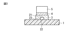
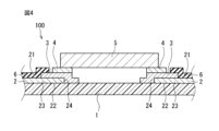
図1から図4を参照しながら、伸縮性デバイス100の構造について説明する。図1は第1実施形態に係る伸縮性デバイスの一部上面図である。図2Aおよび図2Bは伸縮性配線の拡大斜視図である。図3は図1のIII-III断面図である。図4は図1のIV-IV断面図である。なお、図4で示したように第1絶縁層6は多段構造になっており、図1では段差の生じている部分を直線で示している。
図1から図4を参照しながら、伸縮性デバイス100の構造について説明する。図1は第1実施形態に係る伸縮性デバイスの一部上面図である。図2Aおよび図2Bは伸縮性配線の拡大斜視図である。図3は図1のIII-III断面図である。図4は図1のIV-IV断面図である。なお、図4で示したように第1絶縁層6は多段構造になっており、図1では段差の生じている部分を直線で示している。
伸縮性デバイス100は伸縮性基材1上に、伸縮性配線2が引き回されており、電子部品5が実装されている。図1は、電子部品5が実装されている領域を拡大した一部上面図である。なお、伸縮性デバイス100の形状は特に限定されず、伸縮性基材1の厚み方向から見て、矩形状であってもよいし、円形であってもよい。また、伸縮性配線2の配置は特に限定されない。図1では伸縮性基材1の長手方向を両矢印Xで示している。なお、本実施形態において伸縮性デバイス100が伸縮する方向は、伸縮性基材1の長手方向と一致するが、一致していなくてもよい。
伸縮性デバイス100は、伸縮性基材1と、伸縮性基材1上に設けられた伸縮性配線2と、伸縮性配線2に接触する導電性部材3と、導電性部材3上に設けられ、導電性部材3に接触するはんだ部材4と、はんだ部材4を介して導電性部材3に電気的に接続される電子部品5と、伸縮性配線2の少なくとも一部を覆う第1絶縁層6と、を備える。
以下、これらの構成要素の配置について、図1及び図4を参照して説明する。図1に示すように、伸縮性基材1上に伸縮性配線2が設けられている。また、図4に示すように伸縮性配線2の上面21及び端面24に導電性部材3が接触している。
伸縮性基材1は、シート状あるいはフィルム状の伸縮可能な基材であり、例えば、伸縮性を有する樹脂材料から構成される。樹脂材料としては、例えば、熱可塑性ポリウレタン等が挙げられる。伸縮性基材1の厚さは特に限定されないが、生体に貼り付けた際に生体表面の伸縮を阻害しない観点からは、1mm以下であることが好ましく、100μm以下であることがより好ましく、50μm以下であることがさらに好ましい。また、伸縮性基材1の厚さは、1μm以上であることが好ましい。
伸縮性配線2は、伸縮性基材1の主面上にて所定パターンに引き回されている伸縮性配線2のうち、電子部品5に直接的に接続されているものを指す。すなわち、伸縮性デバイス100は、電子部品5に接続されていない配線を有していてもよい。伸縮性配線2は導電性粒子と樹脂とを含んでいる。例えば、導電性粒子としてのAg、Cu、Niなどの金属粉と、シリコーン樹脂などのエラストマー系樹脂とからなる混合物が挙げられる。導電性粒子の平均粒径は特に限定されるものではないが、0.01μm以上、10μm以下であることが好ましい。また、導電性粒子の形状は球形であることが好ましい。
伸縮性配線2の厚さは特に限定されないが、100μm以下であることが好ましく、50μm以下であることがより好ましい。また、伸縮性配線2の厚さは0.01μm以上であることが好ましい。伸縮性配線2の線幅は特に限定されないが0.1μm以上であることが好ましく、10mm以下であることがより好ましい。また、伸縮性配線2に含まれる伸縮性配線2の本数は特に限定されない。
導電性部材3は伸縮性配線2よりもはんだ喰われが発生しにくい物を用いることが好ましい。具体的には、導電性部材3が熱硬化性樹脂を含むことが好ましい。熱硬化性樹脂を含む導電性部材3の例としては、金属フィラーと熱硬化性樹脂を含む樹脂との化合物などが挙げられる。また、金属フィラーの例として、銀フィラー、銅フィラー、ニッケルフィラーなどが挙げられる。このように、導電性部材3が熱硬化性樹脂を含むことで、伸縮性配線2と半田部材4との反応によるはんだ喰われを抑制することができる。なお、導電性部材3は金属箔や金属めっきなどを用いてもよい。
はんだ部材4は特に限定されないが、スズ及びビスマスを金属成分として含むことが好ましく、いわゆる低温はんだであることが好ましい。低温はんだを用いることで、伸縮性基材1、伸縮性配線2及び電子部品5の耐熱温度が低い場合であっても、これらを損傷させることなく電子部品5の実相を行うことができる。
電子部品5は特に限定されないが、例えば増幅器(オペアンプ、トランジスタ等)、ダイオード、集積回路(IC)、コンデンサ、抵抗器、インダクタ等が挙げられる。
第1絶縁層6は、樹脂材料、又は、樹脂材料及び無機材料からなる混合物であることが好ましく、樹脂材料として例えば、ウレタン系、スチレン系、オレフィン系、シリコーン系、フッ素系、ニトリルゴム、ラテックスゴム、塩化ビニル、エステル系、アミド系等のエラストマー系樹脂、エポキシ、フェノール、アクリル、ポリエステル、イミド系、ロジン、セルロース、ポリエチレンテレフタレート系、ポリエチレンナフタレート系、ポリカーボネート系樹脂が挙げられる。
また、伸縮性配線2における導電性部材3と接触する側の端部の外表面が、導電性部材3と導電性部材3に連続する第1絶縁層6とに接触している。
本明細書中における、外表面とは、伸縮性配線2の表面のうち、基材側の表面を除いた表面のことを指す。図2Aを参照して具体的に説明する。図2Aで示したように、例えば伸縮性配線2の表面は上面21、下面22、側面23及び端面24によって構成される。本明細書中で下面とは、伸縮性基材1に最も近い表面のことを指し、上面とは下面に対向する表面のことを指す。第1実施形態に係る伸縮性デバイス100では、上面21が導電性部材3に接し、下面22が伸縮性基材1に接している。なお、伸縮性配線2は図2Aで示したような直方体状に限定されず、曲面や凹凸を有していてもよい。同様に各表面は、矩形状でなくてもよく、角部がRを有していてもよい。
なお、伸縮性配線2は図2Bに示すように、多段構造になっていてもよい。伸縮性配線2が多段構造である場合、上面21及び下面22が複数存在することとなる。このような場合、図2Bに示すように伸縮性基材1の厚み方向において、最も電子部品5に近い上面を最上面21A、2番目に電子部品に近い上面を第2上面21Bとする。なお、伸縮性配線2は第3上面を備えていてもよく、上面の数は特に限定されない。
また、下面22については、伸縮性基材1の厚み方向において、最も伸縮性基材1に近い下面を最下面22Aとし、2番目に近い下面を第2下面22Bとする。なお、伸縮性配線2は第3下面を備えていてもよく、下面の数は特に限定されない。
図2Bのような構造の場合、基材1に最も近い表面は最下面22Aである。すなわち、第2下面22Bは外表面に含むが、最下面22Aは外表面に含まない。同様に伸縮性配線2が第3下面や第4下面を有していても、外表面には含まない。
上面21及び下面22は、実際の上下と一致していなくてもよい。説明の便宜上の名称であって、伸縮性デバイス100の使用時に下面が上面より上側に配置されていてもよい。なお、下面22と伸縮性基材1は接していなくてもよい。後述するように、下面22と伸縮性基材1の間に絶縁層や薄膜が配置されていてもよい。
側面23及び端面24は、上面21と下面22を接続する。伸縮性配線2は2つの側面23と2つの端面を備えるが、図2Aおよび図2Bでは2つの端面のうち一つの図示を省略している。なお、本明細書中では導電性部材3と接触する伸縮性配線2の端面を24とする。伸縮性配線2全体の外表面は上面21、側面23及び両端面によって構成され、伸縮性配線2における導電性部材3と接触する側の端部の外表面とは、上面21、側面23及び端面24によって構成される。なお、伸縮性配線2の導電性部材3と接触する側の端部とは、端面24から導電性部材3の配線の延伸方向における両端部のうち、端面24からより遠い端部(端部Aとする)までを含むことが好ましく、端部Aまでに加えて0.5mmを含むことがより好ましく、端部Aまでに加えて1mmを含むことがより好ましい。このような構造にすることで、伸縮性配線2とはんだ部材4との接触をより確実に抑制することができる。
また、伸縮性配線2以外の各構成要素の各表面についても同様に決定する。なお、本明細書中では伸縮性配線2の上面21を、省略して上面21として記載する。言い換えれば。各表面に符号をつけて記載した場合、伸縮性配線2の各表面のことを指す。そのほかの構成要素の表面については、記載を省略せず符号をつけずに説明する。
このような構造にすることで、伸縮性配線2の外表面が導電性部材3及び第1絶縁層6によって覆われることとなる。すなわち、伸縮性配線2とはんだ部材4とが接触しにくくなるため、はんだ喰われを抑制し、100の信頼性を高めることができる。
また、第1絶縁層6は導電性部材3と連続している。言い換えれば、図4に示すように、第1絶縁層6と導電性部材3とが接触している。仮に、第1絶縁層6と導電性部材3とが接触していない場合、はんだ部材4が、導電性部材3の表面から、導電性部材3の両端面のうち伸縮性配線2上に設けられている端面を介して、伸縮性配線2と接触してしまう恐れがある。第1絶縁層6と導電性部材3とが連続していることで、はんだ喰われの発生を抑制することができる。
なお、導電性部材3と第1絶縁層6とが連続する、とは導電性部材3の端面と第1絶縁層6の端面のみが接触していてもよいが、平面視で、第1絶縁層6が導電性部材3の端部に重なることが好ましい。言い換えれば、図4に示したように、第1絶縁層6の一部が導電性部材3の上に設けられていることが好ましい。はんだ部材4の濡れ広がりが、第1絶縁層6との接触箇所で止まることとなる。すなわち、このような構造にすることで、はんだ部材4の濡れ広がりを抑制することができる。なお、第1絶縁層6とはんだ部材4は接触していてもよいし、図4で示したように接触していなくてもよい。
また、第1絶縁層6が、導電性部材3の上に設けられることで導電性部材3が電子部品側に移動することを防止できる。言い換えれば、導電性部材3と伸縮性配線2との接続性能を上昇させることができる。伸縮デバイス100が伸縮性配線2の延伸方向に伸縮した際、伸縮量の差から伸縮性配線2と導電性部材3とが剥離することが想到される。第1絶縁層6を導電性部材3の上に設けることで、伸縮性配線2と導電性部材3との接続性能を増加させ、剥離を抑制することができる。
なお、図1で示したように、伸縮性配線2の幅方向長さは、導電性部材3の同方向長さより小さいことが好ましい。このような構造にすることで、伸縮性配線2の両側面23に導電性部材3が接することとなり、伸縮性配線2とはんだ部材4との接触を抑制することができる。したがって、接続の信頼性が高まる。
接続性の観点からは、伸縮性配線2と導電性部材3との接触面積は大きいことが好ましい。すなわち、図3及び図4に示すように、導電性部材3が配線の上面21、両側面23及び端面24と接触していることが好ましい。なお、導電性部材3の全体が伸縮性配線2上に設けられていてもよい。
はんだ部材4は導電性部材3の上面に接触している。なお、はんだ部材4は導電性部材3の上面以外と接していてもよい。具体的には、伸縮性基材1の厚み方向から見て、導電性部材3のうち伸縮性配線2と重なっていない端面や両側面と接していてもよい。また、伸縮性基材1と接していてもよい。また、形状は特に限定されない。例えばフィレットを有していてもよい。
はんだ部材4は濡れ広がるため、正確に面積をコントロールすることが困難である。すなわち、前述したように、伸縮性基材1の厚み方向から見て、伸縮性配線2と重なる導電性部材3の表面と接するようにはんだ部材4を配置すると、はんだ部材4が意図せず濡れ広がることで、伸縮性配線2とはんだ部材4が接触してしまいはんだ喰われが発生する虞がある。
電子部品5ははんだ部材4を介して導電性部材3及び伸縮性配線2に電気的に接続されている。なお、電子部品5は図1及び図4に示したように、2本の伸縮性配線2に電気的に接続されているが、例えば4本の伸縮性配線2に電気的に接続されていてもよい。
第1絶縁層6は伸縮性配線2の少なくとも一部を覆っているが、その大きさは特に限定されないが、伸縮性配線2の全体を覆っていることが好ましい。なお、図1で示したように伸縮性配線2の全体に加えて、伸縮性基材1の1部に接触するように設けられていてもよいし、伸縮性基材1の全体を覆っていてもよい。
また、伸縮性配線2の導電性部材3と接触する側の端部の外表面が、導電性部材3と第1絶縁層6とに接触している。前述したように、伸縮性配線2の外表面は、上面21、両側面23、導電性部材3と接触している端面24である。
図3に示したように伸縮性配線2の幅方向長さが導電性部材3の同方向長さより小さいため、導電性部材3と両側面23とが接触している。このような構造の場合、導電性部材3の上面に設けられたはんだ部材4が濡れ広がったとしても、両側面23に接触することはない。なお、導電性部材3は両側面23の全体に接触している必要は無く、一部接触していなくてもよい。
端面24も同様に、はんだ部材4が導電性部材3の伸縮性基材1と接する側の端面を介して濡れ広がったとしても、はんだ部材4と端面24とが接することはない。なお、導電性部材3は端面24の全体に接している必要は無く、一部が接していればよい。
上面21は導電性部材3と導電性部材3に連続する第1絶縁層6とに接触している。前述した通り、このような構造にすることで、導電性部材3の両端面のうち伸縮性配線2上に設けられている端面を介した、はんだ部材4と伸縮性配線2との接触を抑制できる。すなわち、上記の構成にすることで、導電性部材3の両側面及び両端面を介してはんだ部材4と伸縮性配線2との接触を抑制し、伸縮性デバイス100の信頼性を高めることができる。
なお、第1絶縁層6は導電性部材3の端部と接していることが好ましい。言い換えれば、第1絶縁層6は導電性部材3の一方端面、両側面及び上面と接していることが好ましい。このように配置することで、導電性部材3の端部を介した、はんだ部材4と伸縮性配線2の接触を抑制することができる。
また、伸縮性デバイス100が使用時に伸縮する場合、各構成要素の界面で剥離が発生する恐れがある。第1絶縁層6が、導電性部材3上に設けられているとき、基板の厚み方向から見て、第1絶縁層6,導電性部材3及び伸縮性配線2が重なることとなる。このような配置にすることで、第1絶縁層6によって、導電性部材3が上方向への移動を抑制できる。したがって、上面21と導電性部材3との界面が上下への剥離を低減することができる。
なお、各構成要素の厚みは図4で示したものに限定されない。図4では伸縮性配線2の厚みより第1絶縁層6の厚みが大きいが、その逆であってもよい。また、第1絶縁層6のうち、伸縮性配線2上に設けられた部分の厚みと、導電性部材3上に設けられた部分の厚みとは同じであってもよいし、異なっていてもよい。導電性部材3のうち、伸縮性配線2上に設けられた部分の厚みと、伸縮性基材1上に設けられた部分の厚みとは同じであってもよいし、異なっていてもよい。
[第1実施形態の第1変形例]
図5は第1実施形態の第1変形例に係る伸縮性デバイス100Aの一部断面図である。伸縮性デバイス100Aは、第1実施形態に係る伸縮性デバイス100と比較して、導電性部材3及びはんだ部材4の配置が相違する。
図5は第1実施形態の第1変形例に係る伸縮性デバイス100Aの一部断面図である。伸縮性デバイス100Aは、第1実施形態に係る伸縮性デバイス100と比較して、導電性部材3及びはんだ部材4の配置が相違する。
また、第1絶縁層6の一部が導電性部材3とはんだ部材4の両方に接触していることが好ましい。前述したように、伸縮性配線2とはんだ部材4とが接触するとはんだ喰われが生じる可能性がある。同様に、導電性部材3とはんだ部材4とが接触した場合、導電性部材3に対してもはんだ喰われが生じる可能性がある。導電性部材3とはんだ部材4との接触面積が大きければ大きいほど、導電性部材3にはんだ喰われが発生する可能性が高まる。
しかし、はんだ部材4の接続性能は他の部材との接触面積の影響が大きい。すなわち、はんだ部材4の接触面積が少ないと、伸縮時にはんだ部材4の界面が破断し、不良が生じる危険性が高まる。すなわち、導電性部材3とはんだ部材4との接触面積を増加させることなく、はんだ部材4が接触する面積を増加させることが好ましい。
はんだ部材4とはんだ喰われが生じにくい部材との接続面積を増加させることで、導電性部材3のはんだ喰われを抑制し、かつ、はんだ部材4の接触面積を増加させることによって、伸縮時にはんだ部材4の界面が破断することを抑制することができる。上記のような構造にすることで、はんだ喰われの発生しにくい第1絶縁層6とはんだ部材4との接触面積を増加させている。
また、平面視で、第1絶縁層6と導電性部材3とはんだ部材4とが相互に重なることがより好ましい。上述した部分は、平面視において伸縮性配線2とも重なることとなる。すなわち、より伸縮性配線2と、導電性部材3とが上下に破断する可能性を低減できる。
また、はんだ部材4が第1絶縁層6と配線の延伸方向において接触していることがより好ましい。導電性部材3に熱硬化性樹脂が含まれる場合など、導電性部材3が伸縮性配線2よりも伸縮性が悪い場合、導電性部材3の平面視における面積を増加させると、伸縮性デバイス100Aの伸縮性が大きく減少してしまう。しかし、導電性部材3の面積を減少させると、はんだ部材4との接続面積も低下し、接続性能が低下してしまう。はんだ部材4が第1絶縁層6と配線の延伸方向において接触していることで、はんだ部材4と導電性部材3との接続面積を増加させ、接続性能を上昇させることができる。
同様に、平面視において、はんだ部材4の全体が、導電性部材3に重なることが好ましい。導電性部材3とはんだ部材4との接続面積を増加させ、接続性能を上昇させることができる。
また、図5に示すように、第1絶縁層6の一部が、はんだ部材4と導電性部材3との間に配置されていることがさらに好ましい。図5のように、絶縁層の端面に加えて上面の一部もはんだ部材4と接触するため、はんだ部材4の接触面積が増加する。すなわち、はんだ部材4の剥離を抑制することができるとともに、はんだ部材4と導電性部材3との接触面積を増加させることができる。なお、はんだ部材4の一部が、導電性部材3と第1絶縁層6の間に配置されていてもよい。
なお、導電性部材3とはんだ部材4の間に配置される第1絶縁層6の厚みは特に限定されない。伸縮性配線2上に設けられた第1絶縁層6の厚みと同じであってもよいし、異なっていてもよい。
[第1実施形態の第2変形例]
図6は第1実施形態の第2変形例に係る伸縮性デバイス100Bの一部断面図である。伸縮性デバイス100Bは第1実施形態に係る伸縮性デバイス100と比較して、伸縮性配線2及び導電性部材3の配置が相違する。
図6は第1実施形態の第2変形例に係る伸縮性デバイス100Bの一部断面図である。伸縮性デバイス100Bは第1実施形態に係る伸縮性デバイス100と比較して、伸縮性配線2及び導電性部材3の配置が相違する。
図6に示すように伸縮性デバイス100B、伸縮性配線2の一部が導電性部材3上に配置され、伸縮性基材1の長手方向における伸縮性配線2の一部とはんだ部材4との間に第1絶縁層6が配置されている。このような構成にすることで、導電性部材3の一方端面と上面が伸縮性配線2に接触するため、伸縮時の破断を抑制することができる。
なお、このように伸縮性配線2の一部が導電性部材3上にある場合、伸縮性配線2とはんだ部材4との接触を抑制するため、両者の間に第1絶縁層6が配置されることが好ましい。第1絶縁層6によって、伸縮性配線2のはんだ喰われを抑制することができる。
また、このように配置することによって、伸縮性配線2と導電性部材3との接触面積を増加させながら、導電性部材3の厚みを均一に近づけることができる。図6に示すように、平面視において、電子部品5は伸縮性基材1、導電性部材3及びはんだ部材4に重なる。すなわち、これら3つの部材によって電子部品5の平坦性が定まる。電子部品5の平坦性が損なわれると、部品の信頼性が低下する。すなわち、このような構造にすることで、伸縮性配線2と導電性部材3との接触面積を増加させながら、部品の信頼性低下を抑制できる。
第1絶縁層6の形状は特に限定されず、図6に示したように厚みを一定にすることで、導電性部材3の凹凸に合わせた形状にしてもよいし、厚みを変化せて印刷することで上面の高さを一致させてもよい。
[第1実施形態の第3変形例]
図7は第1実施形態の第3変形例に係る伸縮性デバイス100Cの一部断面図である。伸縮性デバイス100Cは、第1実施形態に係る伸縮性デバイス100と比較して、第1絶縁層6が相違する。
図7は第1実施形態の第3変形例に係る伸縮性デバイス100Cの一部断面図である。伸縮性デバイス100Cは、第1実施形態に係る伸縮性デバイス100と比較して、第1絶縁層6が相違する。
図7に示すように、伸縮性デバイス100Cでは伸縮性配線2の一部が導電性部材3の下に配置される。このように配置することで、上面21と端面24とが伸縮性配線2と接触することとなる。すなわち、伸縮性配線2と導電性部材3との接触面積を増加させ、伸縮時の破断を抑制することができる。
また、伸縮性配線2は、厚みの大きい第1部分7と第1部分7よりも厚みが小さい第2部分8とを備え、第2部分8の少なくとも一部は導電性部材3の下に配置されることが好ましい。上述したように、伸縮性配線2の一部が導電性部材3の下に配置されることで、上面21と端面24とが導電性部材3に接触するように配置することができる。
平面視において、導電性部材3のうち伸縮性配線2に重なる部分と、伸縮性配線2に重ならない部分とでは伸縮性基材1からの最短距離が第2部分8の厚みの分だけ異なる。すなわち、第2部分8の厚みが大きいと、導電性部材3の凹凸が大きくなり、平坦性を損なってしまう。
すなわち、伸縮性配線2のうち厚みが小さい第2部分8の少なくとも一部を導電性部材3の下に配置することで、伸縮性配線2と導電性部材3との接触面積を増加させるとともに、導電性部材3の平坦性の損失を抑制できる。また、電子部品5が実装されている領域を低背化することができる。
なお、第2部分8の長さは特に限定されない。図7に示したように第2部分8の一部が導電性部材3の下に配置されていてもよいし、第2部分8の全体が導電性部材3の下に配置されていてもよい。
[第1実施形態の第4変形例]
図8は第1実施形態の第4変形例に係る伸縮性デバイス100Dの一部断面図である。伸縮性デバイス100Dは、第1実施形態に係る伸縮性デバイス100と比較して、伸縮性配線2及び第1絶縁層6の配置が相違する。
図8は第1実施形態の第4変形例に係る伸縮性デバイス100Dの一部断面図である。伸縮性デバイス100Dは、第1実施形態に係る伸縮性デバイス100と比較して、伸縮性配線2及び第1絶縁層6の配置が相違する。
伸縮性配線2の一部は、導電性部材3の上面及び下面にそれぞれ接触することが好ましい。具体的には図8で示したように、伸縮性配線2が二又に分かれており、その間に導電性部材3が配置されていることが好ましい。
例えば、伸縮性配線2を一度印刷した後、その一部と重なるように導電性部材3を印刷し、再度伸縮性配線2を印刷することで図8のような構造を得ることができる。なお、上記の印刷方法はあくまで一例であって、異なる製法を用いてもよい。
上記のような構造にすることで、伸縮性配線2は導電性部材3の一方端面、上面及び下面に接触する。すなわち、接触面積が増加することとなり、接続時の信頼性が増加する。また、前述したように、導電性部材3の上面と接触している伸縮性配線2が、導電性部材3と導電性部材3の下面と接触している伸縮性配線2との剥離を抑制できる。
同様に、導電性部材3の下面と接触している伸縮性配線2が、導電性部材3と導電性部材3の上面と接触している伸縮性配線2との剥離を抑制できる。言い換えれば、伸縮性配線2が導電性部材3の上下に配置されていることで、導電性部材3の変異を抑制することができる。さらに、伸縮性配線2が導電性部材3の上面及び下面と接触していることで、仮にどちらかの接触部分が剥離してしまった際に、もう一方の接触部分で電気的な接続を確保できる。
なお、伸縮性配線2のうち、導電性部材3の上面と接触している部分及び下面と接触している部分の厚みは同じであってもよいし、異なっていてもよい。また、長さについても特に限定されず、図8に示すように、導電性部材3の下面に接触している部分が、導電性部材3の上面に接触している部分より長くてもよいし、同じであってもよいし、上面に接触している部分のほうが長くてもよい。
また、伸縮性基材1の長手方向における伸縮性配線2の一部とはんだ部材4との間に第1絶縁層6が配置されている。このような構成にすることで、導電性部材3の一方端面と上面が伸縮性配線2に接触するため、伸縮時の破断を抑制することができる。
[第1実施形態の第5変形例]
図9は第1実施形態の第5変形例に係る伸縮性デバイス100Eの一部断面図である。伸縮性デバイス100Eは、第1実施形態に係る伸縮性デバイス100と比較して、第2絶縁層9を備える点で相違する。
図9は第1実施形態の第5変形例に係る伸縮性デバイス100Eの一部断面図である。伸縮性デバイス100Eは、第1実施形態に係る伸縮性デバイス100と比較して、第2絶縁層9を備える点で相違する。
第2絶縁層9は、樹脂材料、又は、樹脂材料及び無機材料からなる混合物であることが好ましく、樹脂材料として例えば、ウレタン系、スチレン系、オレフィン系、シリコーン系、フッ素系、ニトリルゴム、ラテックスゴム、塩化ビニル、エステル系、アミド系等のエラストマー系樹脂、エポキシ、フェノール、アクリル、ポリエステル、イミド系、ロジン、セルロース、ポリエチレンテレフタレート系、ポリエチレンナフタレート系、ポリカーボネート系樹脂が挙げられる。第1絶縁層6と同一の材料であってもよいし、異なった材料でもよい。
第2絶縁層9をさらに備え、導電性部材3を基準として第1絶縁層6と接触する側とは反対側の端部に、第2絶縁層9が接触していることが好ましい。導電性部材3と上面21の剥離を抑制するために、導電性部材3と重なるように第1絶縁層6を設けることが好ましいことは前述したとおりである。第2絶縁層9は、導電性部材3と端面24の剥離を抑制することができる。
具体的には図9に示したように、導電性部材3のうち平面視において電子部品5と重なる側の端部に第2絶縁層9が配置されている。このように配置することで、導電性部材3が伸縮性配線2と逆方向に移動することを抑制できる。すなわち、導電性部材3と端面24との剥離を抑制することができる。
また、第2絶縁層9の一部が導電性部材3の端部上に設けられていることが好ましく、第2絶縁層9の一部がはんだ部材4と導電性部材3との間に配置されていることがさらに好ましい。第1絶縁層6と同様に、導電性部材3又ははんだ部材4との接続面積を増加させることで、剥離を抑制することができる。また、第2絶縁層9ははんだ部材4と配線の延伸方向において接触していることが好ましい。第1絶縁層6と同様に、はんだ部材4と導電性部材3との面積を最大化することができる。
また、第2絶縁層9の一部が導電性部材3の端部上に設けられていることで、導電性部材3が電子部品5方向に移動することを抑制できる。すなわち、伸縮性基材1と導電性部材3との剥離を抑制することができる。
また、相互に離隔対向する2つの伸縮性配線2を備え、前記第2絶縁層9が、一方の伸縮性配線2と接触する導電性部材3を基準として第1絶縁層6と接触する側とは反対側の端部と、他方の伸縮性配線2と接触する導電性部材3を基準として第1絶縁層6と接触する側とは反対側の端部とにそれぞれ接触することが好ましい。
具体的には図9で示したように、複数の伸縮性配線2のそれぞれに接触する複数の導電性部材3を備え、第2絶縁層9が複数の導電性部材3に接触している。このように離隔対向する伸縮性配線2に対して、一体となった第1絶縁層を設けることで、作用反作用の法則によって両者の剥離をより抑制することができる。
すなわち、一方の導電性部材3と第1絶縁層6とが伸縮性基材1の長手方向に剥離するような力が働いたとき、他方の導電性部材3がその剥離を抑制することができる。他方の導電性部材3と第1絶縁層6とが伸縮性基材1の長手方向に剥離する場合、一方の導電性部材3と第1絶縁層6が剥離を抑制する。なお、伸縮性基材1の長手方向に剥離する虞のある接触部は、導電性部材3と第1絶縁層6に限定されない。例えば、図9に示すように端面24と、導電性部材3との接続部について伸縮性基材1の長手方向への剥離を抑制することができる。なお、剥離の起こりやすい伸縮性基材1の長手方向、すなわち伸縮方向について説明したが、離隔対向する方向については特に限定されない。
また、電子部品5に接続される伸縮性配線2の本数が特に限定されないことは前述したとおりである。相互に離隔対向する伸縮性配線2の組が複数ある場合、それぞれの組に対して第2絶縁層9を設けていることが好ましく、全ての導電性部材3に接触する第2絶縁層9を設けることが好ましい。すなわち、平面視で電子部品5に重なる領域の凹凸が減少するため、電子部品5を安定して配置することができる。
[第2実施形態]
図10は第2実施形態に係る伸縮性デバイス101の一部断面図である。伸縮性デバイス101は第1実施形態に係る伸縮性デバイス100と比較して、保護層10を備える点で相違する。
図10は第2実施形態に係る伸縮性デバイス101の一部断面図である。伸縮性デバイス101は第1実施形態に係る伸縮性デバイス100と比較して、保護層10を備える点で相違する。
保護層10は伸縮性配線2を水分から保護するための層である。伸縮性配線2が水分を吸収するとイオンマイグレーションが発生し、異なる電位の配線と通電することで短絡する虞がある。保護層10を設けることで、伸縮性配線2のイオンマイグレーションを抑制できる。
保護層10は、樹脂材料、又は、樹脂材料及び無機材料からなる混合物であることが好ましく、樹脂材料として例えば、ウレタン系、スチレン系、オレフィン系、シリコーン系、フッ素系、ニトリルゴム、ラテックスゴム、塩化ビニル、エステル系、アミド系等のエラストマー系樹脂、エポキシ、フェノール、アクリル、ポリエステル、イミド系、ロジン、セルロース、ポリエチレンテレフタレート系、ポリエチレンナフタレート系、ポリカーボネート系樹脂が挙げられる。第1絶縁層6や第2絶縁層9と同一の材料であってもよいし、異なった材料でもよい。
保護層10として吸水性の観点から、保護層10は吸水率の高い部材を選択することが好ましい。また、第1絶縁層6、第2絶縁層9及び保護層10について同一の部材を選択することで、伸縮性配線2の外表面を覆う部材が、導電性部材3を除いて同一となるため印刷時の形成が容易となり、不良の発生リスクを低減できる。
なお、保護層10は図10に示したように、複数の伸縮性配線2の下面22に接触するように一体となって配置されていてもよいし、それぞれの伸縮性配線2ごとに、離隔して配置されていてもよい。また、導電性部材3と伸縮性基材1との間に、保護層10が配置されていることが好ましい。導電性部材3の接触面積を増加させ、破断を抑制することができる。
[第3実施形態]
図11は第3実施形態に係る伸縮性デバイス102の一部断面図である。伸縮性デバイス102は、第1実施形態に係る伸縮性デバイス100と比較して、樹脂層11を備える点で相違する。
図11は第3実施形態に係る伸縮性デバイス102の一部断面図である。伸縮性デバイス102は、第1実施形態に係る伸縮性デバイス100と比較して、樹脂層11を備える点で相違する。
図11に示すように電子部品5を覆う、樹脂層11をさらに備えている。樹脂層11は電子部品5を外力から保護することができる。
樹脂層11の材料としては、ポリ塩化ビニル、ポリエチレン、ポリスチレン、ポリカーボネート、ポリフッ化ビニリデン、ポリイミド、液晶ポリマー、ポリテトラフルオロエチレン、フェノール樹脂、エポキシ系樹脂、ウレタン系樹脂、アクリル系樹脂、シリコーン系樹脂、スチレン・ブタジエン系樹脂等のエラストマー系樹脂、等が挙げられる。
樹脂層11を設ける際に、樹脂層11に含まれる樹脂の硬化に伴い伸縮性デバイス100が収縮する。すなわち、伸縮性デバイス100の、各構成要素の界面が収縮時に剥離する虞がある。上述したように、第1絶縁層6を導電性部材3の上に設けることで、樹脂効果時の収縮による剥離を抑制することができる。その他の剥離抑制効果についても同様である。
樹脂層11は、平面視において、はんだ部材4の全体に重なることが好ましく、導電性部材3及びはんだ部材4の全体に重なることがより好ましい。言い換えれば、樹脂層11の表面12が導電性部材3に接することが好ましく、樹脂層11の表面12が第1絶縁層6に接することがより好ましい。図11には、樹脂層11の表面12と第1絶縁層6の接触部を接点13として示している。このように配置することで、上記のような構造にすることで、破断を抑制することができる。
樹脂層11は、電子部品5を外力から保護する役割であるから、伸縮性配線2と比較して伸縮性に劣る。したがって、平面視で樹脂層11と重なる部分と重ならない部分の界面では伸縮量が大きく変化する。伸縮量が大きく変化する部分は、応力が集中しやすいため、破断も発生しやすい。より具体的には、平面視において、はんだ部材4の一部が樹脂層11と重なり、一部が樹脂層11と重ならないような構造だと、はんだ部材4が破断する虞がある。導電性部材3についても同様である。
一方、樹脂層11が平面視において、はんだ部材4の全体に重なるように配置することで、はんだ部材4は樹脂層の内部に含まれることとなる。すなわち、はんだ部材4全体の伸縮量が均一に近づくため、はんだ部材4の破断を抑制することができる。導電性部材3についても同様である。
なお、上記で説明した各実施形態及び各変形例では、第1絶縁層6が導電性部材3を覆っている。本発明は、上記のような構造に限定されず、導電性部材3と第1絶縁層6は連続していればよい。具体的には、導電性部材3の端面と第1絶縁層6は接触し、かつ、平面視で重なっていなくてもよい。
各実施形態は例示であり、本発明は各実施形態に限定されるものではない。また、異なる実施形態で示した構成の部分的な置換又は組み合わせが可能である。
なお、本発明の一実施形態に係る伸縮性デバイスの態様は、以下のとおりである。
<1>
伸縮性基材と、
前記伸縮性基材上に設けられた伸縮性配線と、
前記伸縮性配線に接触する導電性部材と、
前記導電性部材上に設けられ、前記導電性部材に接触するはんだ部材と、
前記はんだ部材を介して前記導電性部材に電気的に接続される電子部品と、
前記伸縮性配線の少なくとも一部を覆う第1絶縁層と、を備え、
前記伸縮性配線における前記導電性部材と接触する側の端部の外表面が、前記導電性部材と該導電性部材に連続する前記第1の絶縁層とに接触している、伸縮性デバイス。
<2>
前記第1絶縁層が前記導電性部材の端部と接触している、<1>に記載の伸縮性デバイス。
<3>
平面視で、前記第1絶縁層が前記導電性部材の端部に重なる、<1>又は<2>に記載の伸縮性デバイス。
<4>
前記第1絶縁層の一部が前記導電性部材と前記はんだ部材の両方に接触している、<3>に記載の伸縮性デバイス。
<5>
平面視で、前記第1絶縁層と前記導電性部材と前記はんだ部材とが相互に重なる、<1>から<4>の何れか一つに記載の伸縮性デバイス。
<6>
前記第1絶縁層の一部が、前記はんだ部材と前記導電性部材との間に配置されている、<5>に記載の伸縮性デバイス。
<7>
前記伸縮性配線の一部が前記導電性部材上に配置され、前記伸縮性配線の一部と前記はんだ部材との間に前記第1絶縁層が配置されている、<1>から<6>の何れか一つに記載の伸縮性デバイス。
<8>
前記伸縮性配線の一部が前記導電性部材の下に配置される、<1>から<7>の何れか一つに記載の伸縮性デバイス。
<9>
前記伸縮性配線は、厚みの大きい第1部分と第1部分よりも厚みが小さい第2部分とを備え、前記第2部分の少なくとも一部は前記導電性部材の下に配置される、<1>から<8>の何れか一つに記載の伸縮性デバイス。
<10>
前記伸縮性配線の一部は、前記導電性部材の上面および下面にそれぞれ接触する、<1>から<9>の何れか一つに記載の伸縮性デバイス。
<11>
第2絶縁層をさらに備え、
前記導電性部材を基準として前記第1絶縁層と接触する側とは反対側の端部に、前記第2絶縁層が接触している、<1>から<10>の何れか一つに記載の伸縮性デバイス。
<12>
前記2絶縁層の一部が前記導電性部材の前記反対側の端部上に配置される、<11>に記載の伸縮性デバイス。
<13>
相互に離隔対向する2つの前記伸縮性配線を備え、
前記第2絶縁層が、一方の前記伸縮性配線と接触する前記導電性部材を基準として前記第1絶縁層と接触する側とは反対側の端部と、他方の前記伸縮性配線と接触する前記導電性部材を基準として前記第1絶縁層と接触する側とは反対側の端部とにそれぞれ接触する、<11>又は<12>に記載の伸縮性デバイス。
<14>
保護層を更に備え、
前記保護層は、前記伸縮性配線と前記伸縮性基材との間に配置される、<1>から<13>の何れか一つに記載の伸縮性デバイス。
<15>
前記電子部品を覆う、樹脂層をさらに備える、<1>から<14>の何れか一つに記載の伸縮性デバイス。
<16>
前記導電性部材は熱硬化性樹脂を含む、<1>から<15>の何れか一つに記載の伸縮性デバイス。
本発明の一実施形態に係る伸縮性デバイスは、電子部品を搭載した状態で用いることができる。
本出願は、日本国特許出願第2021-199233号(出願日:2021年12月8日、発明の名称:「伸縮性デバイス」)に基づくパリ条約上の優先権を主張する。当該出願に開示された内容は全て、この引用により、本明細書に含まれるものとする。
1:伸縮性基材
2:伸縮性配線
3:導電性部材
4:はんだ部材
5:電子部品
6:第1絶縁層
7:第1部分
8:第2部分
9:第2絶縁層
10:保護層
11:樹脂層
12:樹脂層の表面
13:接点
21:上面
21A:最上面
21B:第2上面
22:下面
22A:最下面
22B:第2下面
23:側面
24:端面
100、100A、100B、100C、100D、100E、101、102:伸縮性デバイス
2:伸縮性配線
3:導電性部材
4:はんだ部材
5:電子部品
6:第1絶縁層
7:第1部分
8:第2部分
9:第2絶縁層
10:保護層
11:樹脂層
12:樹脂層の表面
13:接点
21:上面
21A:最上面
21B:第2上面
22:下面
22A:最下面
22B:第2下面
23:側面
24:端面
100、100A、100B、100C、100D、100E、101、102:伸縮性デバイス
Claims (16)
- 伸縮性基材と、
前記伸縮性基材上に設けられた伸縮性配線と、
前記伸縮性配線に接触する導電性部材と、
前記導電性部材上に設けられ、前記導電性部材に接触するはんだ部材と、
前記はんだ部材を介して前記導電性部材に電気的に接続される電子部品と、
前記伸縮性配線の少なくとも一部を覆う第1絶縁層と、を備え、
前記伸縮性配線における前記導電性部材と接触する側の端部の外表面が、前記導電性部材と該導電性部材に連続する前記第1の絶縁層とに接触している、伸縮性デバイス。 - 前記第1絶縁層が前記導電性部材の端部と接触している、請求項1に記載の伸縮性デバイス。
- 平面視で、前記第1絶縁層が前記導電性部材の端部に重なる、請求項1又は2に記載の伸縮性デバイス。
- 前記第1絶縁層の一部が前記導電性部材と前記はんだ部材の両方に接触している、請求項3に記載の伸縮性デバイス。
- 平面視で、前記第1絶縁層と前記導電性部材と前記はんだ部材とが相互に重なる、請求項1から4の何れか一つに記載の伸縮性デバイス。
- 前記第1絶縁層の一部が、前記はんだ部材と前記導電性部材との間に配置されている、請求項5に記載の伸縮性デバイス。
- 前記伸縮性配線の一部が前記導電性部材上に配置され、前記伸縮性配線の一部と前記はんだ部材との間に前記第1絶縁層が配置されている、請求項1から6の何れか一つに記載の伸縮性デバイス。
- 前記伸縮性配線の一部が前記導電性部材の下に配置される、請求項1から7の何れか一つに記載の伸縮性デバイス。
- 前記伸縮性配線は、厚みの大きい第1部分と第1部分よりも厚みが小さい第2部分とを備え、前記第2部分の少なくとも一部は前記導電性部材の下に配置される、請求項1から8の何れか一つに記載の伸縮性デバイス。
- 前記伸縮性配線の一部は、前記導電性部材の上面および下面にそれぞれ接触する、請求項1から9の何れか一つに記載の伸縮性デバイス。
- 第2絶縁層をさらに備え、
前記導電性部材を基準として前記第1絶縁層と接触する側とは反対側の端部に、前記第2絶縁層が接触している、請求項1から10の何れか一つに記載の伸縮性デバイス。 - 前記2絶縁層の一部が前記導電性部材の前記反対側の端部上に配置される、請求項11に記載の伸縮性デバイス。
- 相互に離隔対向する2つの前記伸縮性配線を備え、
前記第2絶縁層が、一方の前記伸縮性配線と接触する前記導電性部材を基準として前記第1絶縁層と接触する側とは反対側の端部と、他方の前記伸縮性配線と接触する前記導電性部材を基準として前記第1絶縁層と接触する側とは反対側の端部とにそれぞれ接触する、請求項11又は12に記載の伸縮性デバイス。 - 保護層を更に備え、
前記保護層は、前記伸縮性配線と前記伸縮性基材との間に配置される、請求項1から13の何れか一つに記載の伸縮性デバイス。 - 前記電子部品を覆う、樹脂層をさらに備える、請求項1から14の何れか一つに記載の伸縮性デバイス。
- 前記導電性部材は熱硬化性樹脂を含む、請求項1から15の何れか一つに記載の伸縮性デバイス。
Applications Claiming Priority (2)
| Application Number | Priority Date | Filing Date | Title |
|---|---|---|---|
| JP2021199233 | 2021-12-08 | ||
| JP2021-199233 | 2021-12-08 |
Publications (1)
| Publication Number | Publication Date |
|---|---|
| WO2023106055A1 true WO2023106055A1 (ja) | 2023-06-15 |
Family
ID=86730404
Family Applications (1)
| Application Number | Title | Priority Date | Filing Date |
|---|---|---|---|
| PCT/JP2022/042512 WO2023106055A1 (ja) | 2021-12-08 | 2022-11-16 | 伸縮性デバイス |
Country Status (1)
| Country | Link |
|---|---|
| WO (1) | WO2023106055A1 (ja) |
Citations (4)
| Publication number | Priority date | Publication date | Assignee | Title |
|---|---|---|---|---|
| WO2009081929A1 (ja) * | 2007-12-26 | 2009-07-02 | Fujikura Ltd. | 実装基板及びその製造方法 |
| JP2016143763A (ja) * | 2015-02-02 | 2016-08-08 | 株式会社フジクラ | 伸縮性回路基板 |
| WO2020203135A1 (ja) * | 2019-03-29 | 2020-10-08 | 株式会社村田製作所 | 伸縮性実装基板 |
| WO2021235282A1 (ja) * | 2020-05-21 | 2021-11-25 | 株式会社村田製作所 | 伸縮性配線基板 |
-
2022
- 2022-11-16 WO PCT/JP2022/042512 patent/WO2023106055A1/ja unknown
Patent Citations (4)
| Publication number | Priority date | Publication date | Assignee | Title |
|---|---|---|---|---|
| WO2009081929A1 (ja) * | 2007-12-26 | 2009-07-02 | Fujikura Ltd. | 実装基板及びその製造方法 |
| JP2016143763A (ja) * | 2015-02-02 | 2016-08-08 | 株式会社フジクラ | 伸縮性回路基板 |
| WO2020203135A1 (ja) * | 2019-03-29 | 2020-10-08 | 株式会社村田製作所 | 伸縮性実装基板 |
| WO2021235282A1 (ja) * | 2020-05-21 | 2021-11-25 | 株式会社村田製作所 | 伸縮性配線基板 |
Similar Documents
| Publication | Publication Date | Title |
|---|---|---|
| JP6518451B2 (ja) | 伸縮性回路基板 | |
| US9402307B2 (en) | Rigid-flexible substrate and method for manufacturing the same | |
| US10083887B2 (en) | Chip component-embedded resin multilayer substrate and manufacturing method thereof | |
| US9332641B2 (en) | Connection structure of circuit board | |
| TWI497535B (zh) | 具有軟性材料層之微電阻元件及其製造方法 | |
| US9686860B2 (en) | Printed circuit board and method of fabricating the same | |
| US10460874B2 (en) | Electronic component with metal terminals | |
| WO2023106055A1 (ja) | 伸縮性デバイス | |
| US10916520B2 (en) | Semiconductor device, and method of manufacturing the same | |
| CN112423472B (zh) | 软硬结合电路板及其制作方法 | |
| KR101846853B1 (ko) | 더미를 이용하여 강성 조절되는 연성 반도체 기판 | |
| TWI699147B (zh) | 軟性電路板及包括其的電子裝置 | |
| JP5372235B2 (ja) | 半導体装置および半導体装置実装体 | |
| JP5006162B2 (ja) | 電気接続部材 | |
| CN107958875B (zh) | 半导体装置以及布线基板的设计方法 | |
| WO2017006665A1 (ja) | 基板およびこれを備える電子機器 | |
| WO2000049652A1 (fr) | Materiau de liaison, dispositif semi-conducteur et procede de fabrication, carte et dispositif electronique | |
| WO2023171464A1 (ja) | 伸縮性デバイス | |
| KR20160046977A (ko) | 이방성 도전입자 | |
| WO2024070591A1 (ja) | 伸縮性デバイス | |
| TWI782100B (zh) | 貫通電極基板及使用有貫通電極基板之半導體裝置 | |
| WO2024070592A1 (ja) | 伸縮性デバイス | |
| JP5750101B2 (ja) | コネクタ | |
| JP2014183086A (ja) | 積層型配線板 | |
| KR101896225B1 (ko) | 회로 기판 및 이의 제조 방법 |
Legal Events
| Date | Code | Title | Description |
|---|---|---|---|
| 121 | Ep: the epo has been informed by wipo that ep was designated in this application |
Ref document number: 22903986 Country of ref document: EP Kind code of ref document: A1 |