WO2023106051A1 - 伸縮デバイス - Google Patents
伸縮デバイス Download PDFInfo
- Publication number
- WO2023106051A1 WO2023106051A1 PCT/JP2022/042423 JP2022042423W WO2023106051A1 WO 2023106051 A1 WO2023106051 A1 WO 2023106051A1 JP 2022042423 W JP2022042423 W JP 2022042423W WO 2023106051 A1 WO2023106051 A1 WO 2023106051A1
- Authority
- WO
- WIPO (PCT)
- Prior art keywords
- wiring
- substrate
- main surface
- board
- side wiring
- Prior art date
- Legal status (The legal status is an assumption and is not a legal conclusion. Google has not performed a legal analysis and makes no representation as to the accuracy of the status listed.)
- Ceased
Links
Images






Classifications
-
- H—ELECTRICITY
- H10—SEMICONDUCTOR DEVICES; ELECTRIC SOLID-STATE DEVICES NOT OTHERWISE PROVIDED FOR
- H10W—GENERIC PACKAGES, INTERCONNECTIONS, CONNECTORS OR OTHER CONSTRUCTIONAL DETAILS OF DEVICES COVERED BY CLASS H10
- H10W70/00—Package substrates; Interposers; Redistribution layers [RDL]
- H10W70/60—Insulating or insulated package substrates; Interposers; Redistribution layers
- H10W70/67—Insulating or insulated package substrates; Interposers; Redistribution layers characterised by their insulating layers or insulating parts
- H10W70/688—Flexible insulating substrates
-
- H—ELECTRICITY
- H05—ELECTRIC TECHNIQUES NOT OTHERWISE PROVIDED FOR
- H05K—PRINTED CIRCUITS; CASINGS OR CONSTRUCTIONAL DETAILS OF ELECTRIC APPARATUS; MANUFACTURE OF ASSEMBLAGES OF ELECTRICAL COMPONENTS
- H05K1/00—Printed circuits
- H05K1/02—Details
-
- H—ELECTRICITY
- H05—ELECTRIC TECHNIQUES NOT OTHERWISE PROVIDED FOR
- H05K—PRINTED CIRCUITS; CASINGS OR CONSTRUCTIONAL DETAILS OF ELECTRIC APPARATUS; MANUFACTURE OF ASSEMBLAGES OF ELECTRICAL COMPONENTS
- H05K1/00—Printed circuits
- H05K1/02—Details
- H05K1/14—Structural association of two or more printed circuits
-
- H—ELECTRICITY
- H10—SEMICONDUCTOR DEVICES; ELECTRIC SOLID-STATE DEVICES NOT OTHERWISE PROVIDED FOR
- H10W—GENERIC PACKAGES, INTERCONNECTIONS, CONNECTORS OR OTHER CONSTRUCTIONAL DETAILS OF DEVICES COVERED BY CLASS H10
- H10W70/00—Package substrates; Interposers; Redistribution layers [RDL]
- H10W70/60—Insulating or insulated package substrates; Interposers; Redistribution layers
- H10W70/62—Insulating or insulated package substrates; Interposers; Redistribution layers characterised by their interconnections
- H10W70/65—Shapes or dispositions of interconnections
-
- H—ELECTRICITY
- H10—SEMICONDUCTOR DEVICES; ELECTRIC SOLID-STATE DEVICES NOT OTHERWISE PROVIDED FOR
- H10W—GENERIC PACKAGES, INTERCONNECTIONS, CONNECTORS OR OTHER CONSTRUCTIONAL DETAILS OF DEVICES COVERED BY CLASS H10
- H10W70/00—Package substrates; Interposers; Redistribution layers [RDL]
- H10W70/60—Insulating or insulated package substrates; Interposers; Redistribution layers
- H10W70/67—Insulating or insulated package substrates; Interposers; Redistribution layers characterised by their insulating layers or insulating parts
- H10W70/68—Shapes or dispositions thereof
- H10W70/685—Shapes or dispositions thereof comprising multiple insulating layers
Definitions
- the present disclosure relates to elastic devices.
- Patent Document 1 Japanese Unexamined Patent Application Publication No. 2017-118109
- the stretchable device includes one stretchable substrate and stretchable wiring formed on one main surface of the stretchable substrate.
- stretchable devices have areas with high wiring density and areas with low wiring density.
- stretchable devices it is very difficult to route stretchable wires on the stretchable substrate in areas with high wiring density. Therefore, if an attempt is made to manufacture a stretchable device using a single stretchable substrate, if a defect occurs in a portion that is difficult to manufacture, all of the stretchable device will become defective, resulting in a decrease in yield.
- manufacturing efficiency will decrease, resulting in a problem of reduced yield.
- an object of the present disclosure is to provide an elastic device that is not difficult to manufacture and can be manufactured with a high yield.
- a stretchable device includes: a first substrate having a first main surface and a second main surface facing each other; a first wiring provided on the first main surface and extending along the first main surface and a second wiring adjacent to the first wiring; a stretchable second substrate having third and fourth major surfaces facing each other; a stretchable third wiring provided on the fourth main surface and extending along the fourth main surface and a stretchable fourth wiring adjacent to the third wiring; the first substrate and the second substrate are connected, The shortest distance between the first wiring and the second wiring is shorter than the shortest distance between the third wiring and the fourth wiring.
- the term “on the main surface” refers to an outward direction between the outer side and the inner side of the substrate bounded by the main surface, rather than an absolute direction such as vertical information defined by the direction of gravity. .
- “on the major surface” is a relative direction determined by the inorganic nature of the major surface.
- “above” an element includes not only the position directly above (on) in contact with the element, but also the position above the element, i.e., the position or distance above the element via another object. Also includes the upper position (above) with a space.
- the shortest distance between the first wiring and the second wiring provided on the first substrate is the distance between the stretchable third wiring and the fourth wiring provided on the stretchable second substrate. are arranged so that they are shorter than the shortest distance between them. Therefore, while fine wiring patterns, which are difficult to manufacture, are formed on the first substrate, the wirings are relatively sparsely distributed on the stretchable second substrate. . Therefore, manufacturing difficulty is not high, and manufacturing can be performed with a high yield.
- the shortest distance between the first wiring and the second wiring is less than 250 ⁇ m, and the shortest distance between the third wiring and the fourth wiring is 250 ⁇ m or more. is.
- the distance between the wirings provided on the first substrate is less than 250 ⁇ m, and the distance between the wirings provided on the second substrate is 250 ⁇ m or more. This makes it easier to adjust the difference in degree, lowers the difficulty of manufacturing the stretchable device, and facilitates manufacturing with a higher yield.
- a first electronic component is provided only on the first main surface, The first electronic component is electrically connected to the first wiring and the second wiring.
- the electronic components are provided only on the first substrate, the degree of difficulty in manufacturing the second substrate is lowered, and it becomes easy to manufacture with a high yield.
- a first electronic component provided on the first main surface; a second electronic component provided on the fourth main surface;
- the first electronic component has a first terminal electrically connected to the first wiring and a second terminal electrically connected to the second wiring, the second electronic component has a third terminal electrically connected to the third wiring and a fourth terminal electrically connected to the fourth wiring;
- the shortest distance between the first terminal and the second terminal is shorter than the shortest distance between the third terminal and the fourth terminal.
- the shortest distance between the first terminal and the second terminal of the first electronic component on the first substrate is
- the degree of difficulty in manufacturing the second substrate is reduced, making it easy to manufacture with high yield.
- a fifth wiring provided on the first main surface,
- the fifth wiring has a region overlapping with the first wiring or the second wiring when viewed from the direction perpendicular to the first main surface.
- wiring with a more complicated structure is arranged on the first substrate, and the wiring structure on the second substrate can be simplified. Therefore, the degree of difficulty in manufacturing the second substrate is lowered, and it becomes easy to manufacture the second substrate with a high yield.
- one embodiment of the stretchable device further comprises a conductive member that electrically connects the first wiring and the third wiring.
- connection reliability can be improved.
- manufacturing difficulty can be lowered.
- the first substrate and the second substrate are arranged such that the first main surface and the fourth main surface face each other; the first wiring and the third wiring are arranged so as to face each other in a direction perpendicular to the first main surface;
- the conductive member is arranged between the first wiring and the third wiring.
- the first substrate and the second substrate can be connected by the conductive member, the mechanical strength of the joint between the first substrate and the second substrate can be enhanced.
- the conductive member includes conductive particles, A particle diameter of the conductive particles is larger than the distance between the first wiring and the third wiring.
- the particle diameter of the conductive particles is larger than the distance between the electrically connected first wiring and the third wiring, the first wiring and the third wiring are more closely connected. A reliable electrical connection is established.
- the stretching device In a section perpendicular to the direction in which the first wiring extends, in a portion where the conductive member, the first wiring, and the third wiring overlap, The width of the first wiring and the width of the third wiring are different.
- the width of the first wiring and the width of the second wiring are different in the portion where the first wiring and the third wiring overlap, doming is suppressed and the first wiring and the third wiring are separated. A reliable electrical connection is possible.
- the stretching device In a cross section perpendicular to the direction in which the first wiring extends in the portion where the first wiring and the third wiring overlap,
- the width of the narrower one of the first wiring and the third wiring is 500 ⁇ m or less.
- the width of the narrower wiring is 500 ⁇ m or less. better connection.
- At least one end of the first wiring and the third wiring has a plurality of teeth provided in parallel and spaced apart in the width direction.
- the interval between two adjacent tooth portions is 700 ⁇ m or less.
- the first wiring and the third wiring are electrically connected more reliably.
- the distances between two adjacent teeth are all the same.
- the plurality of teeth are arranged at equal intervals in the width direction, so that the first wiring and the third wiring are electrically connected more reliably.
- the distance between two adjacent teeth is 200 ⁇ m or more.
- the stretching device Further comprising a first insulating coating layer covering the first wiring,
- the first insulating coating layer overlaps the conductive member when viewed from a direction perpendicular to the first main surface.
- the first wiring is covered with the first insulating coating layer, contact between the first wiring and the outside is suppressed, and noise can be reduced. Furthermore, since the first insulating coating layer extends into the region where the first wiring and the third wiring are electrically connected by the conductive member, breakage of the wiring can be easily suppressed.
- the stretching device Further comprising a second insulating coating layer covering the second wiring,
- the second insulating coating layer overlaps the conductive member when viewed from a direction perpendicular to the fourth main surface.
- the third wiring is covered with the second insulating coating layer, contact between the third wiring and the outside is suppressed, and noise can be reduced. Furthermore, since the second insulating coating layer extends into the area where the first wiring and the third wiring are electrically connected by the conductive member, it becomes easy to suppress the breakage of the wiring.
- the first substrate is stretchable.
- the expansion/contraction load applied to the second substrate can be reduced.
- the first wiring and the second wiring are stretchable.
- the expansion and contraction load applied to the third wiring and the fourth wiring can be reduced.
- a third substrate having a fifth main surface and a sixth main surface facing each other; a sixth wiring and a seventh wiring provided on the fifth main surface and extending along the fifth main surface; the second substrate and the third substrate are connected,
- the shortest distance between the sixth wiring and the seventh wiring is shorter than the shortest distance between the third wiring and the fourth wiring.
- a stretchable device with a more complicated configuration can be manufactured.
- the stretchable device according to one aspect of the present disclosure, it is not difficult to manufacture, and can be manufactured with high yield.
- FIG. 1 is a plan view showing a first embodiment of an elastic device
- FIG. FIG. 2 is a sectional view taken along line II of FIG. 1
- It is a fragmentary cross-sectional view showing the first embodiment of the stretchable device and showing the first substrate-side wiring and the second substrate-side wiring.
- 1 is a cross-sectional view showing a first embodiment of an elastic device
- FIG. 1 is a cross-sectional view showing a first embodiment of an elastic device
- FIG. Fig. 10 is a plan view showing a second embodiment of an elastic device
- FIG. 10 is an enlarged plan view showing the third embodiment of the stretchable device and showing the first substrate-side wiring and the second substrate-side wiring
- FIG. 10 is an enlarged plan view showing the third embodiment of the stretchable device and showing the first substrate-side wiring and the second substrate-side wiring
- FIG. 11 is an enlarged plan view showing the stretchable device according to the fourth embodiment, showing the first substrate-side wiring and the fifth wiring
- FIG. 8 is a cross-sectional view taken along the line II-II of FIG. 7
- FIG. 11 is a partial cross-sectional view showing a fifth embodiment of the stretchable device and showing first substrate-side wiring and second substrate-side wiring
- FIG. 10 is a partial cross-sectional view showing a sixth embodiment of the stretchable device and showing first substrate-side wiring and second substrate-side wiring
- FIG. 11 is a cross-sectional view taken along line III-III in FIG. 10;
- FIG. 11 is a cross-sectional view showing a seventh embodiment of an elastic device;
- FIG. 11 is a plan view showing an eighth embodiment of an elastic device;
- FIG. 20 is a plan view showing a ninth embodiment of an elastic device;
- FIG. 20 is an enlarged plan view showing the ninth embodiment of the elastic device and showing the first substrate-side wiring and the second substrate-side wiring;
- FIG. 20 is an enlarged plan view showing the ninth embodiment of the elastic device and showing the first substrate-side wiring and the second substrate-side wiring;
- FIG. 1 is a plan view showing a first embodiment of an elastic device
- FIG. 2 is a sectional view taken along line II of FIG.
- the stretchable device is used, for example, to contact a living body and measure a biological signal.
- the stretchable device 1 includes a first substrate 11, a plurality of first substrate-side wirings 21 provided on the first substrate 11, and first electronic components 31 provided on the first substrate 11. , a stretchable second substrate 12 , and a plurality of stretchable second substrate-side wirings 22 provided on the second substrate 12 .
- One of the adjacent first substrate-side wirings 21 corresponds to the first wiring described in the claims, and the other corresponds to the second wiring described in the claims.
- one of the adjacent second substrate side wirings 22 corresponds to the third wiring described in the claims, and the other corresponds to the fourth wiring described in the claims.
- the first substrate 11 is made of a resin material such as styrene resin, olefin resin, epoxy resin, urethane resin, polyimide resin, fluorine resin, polyphenylene oxide resin, phenol resin, bismaleimide resin, acrylic resin, or silicone resin. It may contain fibers such as fibers and paper fibers.
- the first substrate 11 may be stretchable. When the first substrate 11 is stretchable, the stretching load applied to the second substrate 12 can be reduced. Also, the first substrate 11 may be a non-stretchable substrate such as a printed circuit board (PCB).
- PCB printed circuit board
- the expansion ratio of the first substrate 11 is preferably 100 to 1000%. By setting the expansion ratio as described above, it is easy to form a wiring having a complicated structure on the first substrate 11 .
- the Young's modulus of the first substrate 11 is preferably 0.1-50 MPa. By setting the Young's modulus as described above, it is easy to form a wiring having a complicated structure on the first substrate 11 .
- the thickness of the first substrate 11 is, for example, 10-100 ⁇ m.
- the first substrate 11 includes a first major surface 111 and a second major surface 112 facing each other.
- the first substrate 11 is formed in a rectangular shape in plan view, and is arranged so that one edge 11 a of the first substrate 11 faces the second substrate 12 .
- the first substrate-side wiring 21 is made of a conductive material.
- a conductive material for example, a metal foil of silver, copper, nickel, or the like may be used.
- a mixture consisting of The thickness of the metal foil is preferably 0.01 ⁇ m or more and 10 ⁇ m or less, and the average particle size D50 of the metal powder is preferably 0.01 ⁇ m or more and 10 ⁇ m or less.
- the shape of the metal powder may be a spherical shape, a flat shape, an irregular shape having projections, or the like.
- the first substrate wiring 21 may be stretchable. When the first board-side wiring 21 is stretchable, the expansion/contraction load applied to the second board-side wiring 22 can be reduced.
- the thickness of the first substrate-side wiring 21 is preferably 100 ⁇ m or less, more preferably 50 ⁇ m or less, and preferably 1 ⁇ m or more, more preferably 10 ⁇ m or more. As the thickness of the first substrate-side wiring 21 is thinner, unevenness is smaller and lamination or the like is easier.
- the width of the first substrate wiring 21 is preferably 100 ⁇ m or more and 10,000 ⁇ m or less, more preferably 300 ⁇ m or more and 4,000 ⁇ m or less.
- the first board-side wiring 21 is arranged on the first main surface 111 . That is, both the first wiring and the second wiring described in the claims are arranged on the first main surface 111 and exist on the same main surface.
- the first substrate-side wiring 21 is formed by screen printing, inkjet printing, dispensing, or etching of metal foil so as to be in direct contact with the first main surface 111 .
- the first substrate-side wiring 21 may be arranged on the first main surface 111 via another member such as an insulating member (not shown). Also, the first substrate-side wiring 21 may be covered with an insulating coating layer (not shown).
- first substrate-side wirings 21 may be two or more.
- first wiring and the second wiring described in the claims refer to any two adjacent wirings among the first substrate-side wirings 21. . That is, the first substrate-side wiring 21 may include wiring other than the first wiring and the second wiring described in the claims.
- the first substrate-side wiring 21 includes a first region overlapping the first electronic component 31 or the terminals of the first electronic component 31 when viewed from the direction perpendicular to the first substrate 11, 1 and a second region that does not overlap the terminals of the electronic component 31 .
- the shortest distance between the first wiring and the second wiring described in the claims refers to the shortest distance between the second regions of each wiring.
- the plurality of first substrate-side wirings 21 extend along the first main surface 111 respectively.
- the plurality of first substrate-side wirings 21 may be arranged separately without intersecting each other.
- the first substrate-side wiring 21 is composed of a straight portion and a corner portion, but is not limited to this, and may have a curved portion.
- the second substrate 12 is made of an elastic resin material such as styrene resin, olefin resin, epoxy resin, urethane resin, acrylic resin, or silicone resin, preferably urethane resin.
- Urethane resins include thermoplastic polyurethane (TPU).
- Styrene resins include styrene-butadiene-styrene copolymer resins (SBS).
- the expansion ratio of the second substrate 12 is preferably 50% or more. By setting the stretch rate to the above range, the stretchable device has good followability to the living body.
- the Young's modulus of the second substrate 12 is preferably 100 MPa or less, more preferably 30 MPa or less. By setting the Young's modulus as described above, it is possible to suppress the user's discomfort.
- the thickness of the second substrate 12 is, for example, 0.1 to 100 ⁇ m.
- the second substrate 12 includes a third main surface 121 and a fourth main surface 122 facing each other.
- the second substrate is formed in a rectangular shape and arranged so that one edge 12a of the second substrate 12 faces one edge 11a of the first substrate 11 .
- the second board-side wiring 22 is made of a stretchable conductive material.
- a stretchable conductive material for example, a mixture of metal powder such as silver, copper, nickel, etc. and elastomeric resin such as silicone is used.
- the second substrate wiring 22 is arranged on the fourth main surface 122 . That is, both the third wiring and the fourth wiring described in the claims are arranged on the fourth main surface 122 and exist on the same main surface.
- Each of the second substrate-side wirings 22 is formed by printing so as to be in direct contact with the fourth main surface 122 .
- the second substrate-side wiring 22 may be arranged on the fourth main surface 122 via another member such as an insulating member (not shown). Also, the second substrate-side wiring 22 may be covered with an insulating coating layer (not shown).
- the number of second substrate side wirings 22 should be two or more.
- the third wiring and the fourth wiring described in the claims refer to any two adjacent wirings among the second substrate-side wirings 22. . That is, the second substrate-side wiring 22 may include wiring other than the third wiring and the fourth wiring described in the claims.
- the plurality of second-board-side wirings 22 extend along the fourth main surface 122 respectively.
- the plurality of second substrate-side wirings 22 may be arranged separately without intersecting each other.
- the second board-side wirings 22 are electrically connected to the first board-side wirings 21 respectively.
- the second substrate-side wiring 22 corresponding to the third wiring may be electrically connected to the first substrate-side wiring 21 corresponding to the first wiring, and the second substrate-side wiring 22 corresponding to the fourth wiring may be electrically connected to , may be electrically connected to the first board-side wiring 21 corresponding to the second wiring.
- the second substrate-side wiring 21 is composed of a straight portion, but is not limited to this, and may have a curved portion.
- the shortest distance d1 between adjacent first board-side wirings 21 is shorter than the shortest distance d2 between adjacent second board-side wirings 22. That is, the wiring pattern arranged on the first principal surface 111 is finer than the wiring pattern arranged on the fourth principal surface 122 . Therefore, while a fine wiring pattern is formed on the first substrate 11, the wirings are relatively sparsely distributed and arranged on the stretchable second substrate 12. FIG. Therefore, manufacturing difficulty is not high, and manufacturing can be performed with a high yield. Furthermore, since the wiring is arranged relatively sparsely distributed on the second substrate 12, the expansion and contraction load can be relatively evenly absorbed by the entire second substrate 12. FIG.
- n be the number of first substrate-side wirings 21, and the shortest distance between wirings will be described for the case where n is 2.
- predetermined first substrate side wirings are 21a, 21b, 21c, and 21d
- predetermined second substrate side wirings are 22a, 22b, 22c, and 22d.
- the shortest distance d1 between the adjacent first substrate wirings 21a and 21b is the distance from one first substrate wiring 21a to the other first substrate wiring 21b along one first substrate wiring 21a. This is the shortest value among the measured values obtained by sequential measurement.
- the shortest distance d2 between the adjacent second-board-side wirings 22a and 22b is from one second-board-side wiring 22a to the other second-board-side wiring 22b along one of the second-board-side wirings 22a.
- d1 is smaller than d2. It means having a value.
- the shortest distance between wirings will be described.
- the shortest distance between adjacent first substrate side wirings 21 means the smallest value among the shortest distances between n ⁇ 1 pairs of adjacent first substrate side wirings 21 .
- the shortest distance between the first set of adjacent first board side wirings 21a and 21b is d11
- the shortest distance between the second set of adjacent first board side wirings 21c and 21d is d12. Comparing the shortest distance d11 and the shortest distance d12, the shortest distance d11 is smaller. By comparing n ⁇ 1 values in this manner, the shortest distance d1, which is the minimum value, can be obtained.
- the shortest distance d2 between adjacent second-board-side wirings 22 is the smallest value among the shortest distances between n-1 pairs of adjacent second-board-side wirings 22 .
- the shortest distance between the first set of adjacent second board side wirings 22a and 21b is d21
- the shortest distance between the second set of adjacent second board side wirings 21c and 21d is d22. Comparing the shortest distance d21 and the shortest distance d22, the shortest distance d21 is smaller. By comparing n ⁇ 1 values in this manner, the shortest distance d2, which is the minimum value, can be obtained.
- the shortest distance between adjacent first substrate wirings 21 is shorter than the shortest distance between adjacent second substrate wirings 22 means that d1 has a smaller value when d1 and d2 are compared. .
- the width of the first board-side wiring 21 is narrower than the width of the second board-side wiring 22 . Since the width of the wiring on the first substrate side is narrower than the width of the wiring on the second substrate side, it is easy to form a finer wiring pattern on the first substrate.
- the stretchable device 1 further includes a conductive member 41 that electrically connects the first board-side wiring 21 and the second board-side wiring 22 .
- the first wiring and the third wiring are electrically connected via the conductive member, so that connection reliability can be improved.
- connection reliability can be improved.
- manufacturing difficulty can be lowered.
- the first substrate 11 and the second substrate 12 are arranged so that the first main surface 111 and the fourth main surface 122 face each other.
- the first board-side wiring 21 and the second board-side wiring 23 are arranged to face each other, and the conductive member 41 is arranged between the first board-side wiring 21 and the second board-side wiring 22. .
- a portion where the first substrate-side wiring 21 and the second substrate-side wiring 22 overlap is generated, and a conductive member 41 exists in this portion, so that the first substrate-side wiring 21 and the second substrate-side wiring 22 are separated from each other by the conductive member. Since it is electrically connected via 41, connection reliability can be further improved.
- the first substrate 11 and the second substrate 12 can be connected by the conductive member 41, the mechanical strength of the joint portion between the first substrate 11 and the second substrate 12 can be enhanced.
- the conductive member 41 is, for example, an anisotropic conductive film (ACF), has conductivity in the direction orthogonal to the first main surface 111, and has insulation in the planar direction.
- Conductive member 41 includes a thermosetting epoxy resin and conductive particles dispersed in the epoxy resin. Therefore, the first substrate-side wiring 21 is conducted only to the immediately above second substrate-side wiring 22, and is conducted to the first substrate-side wiring 21 adjacent in the direction of the first main surface 111 and the second substrate-side wiring 22 that is not directly above. do not.
- the particle diameter of the conductive particles is, for example, 10 to 30 ⁇ m. As shown in FIG. 3, it is preferably larger than the distance in the direction perpendicular to the first main surface 111 between the first substrate-side wiring 21 and the second substrate-side wiring 22 .
- the surfaces of the conductive particles are conductive, and if the particle diameter of the conductive particles is larger than the distance between the first substrate-side wiring 21 and the second substrate-side wiring 22 that are electrically connected, the conductive particles are conductive. Since the surface of the conductive particles and the wiring are in more reliable contact, the first substrate-side wiring 21 and the second substrate-side wiring 22 are electrically connected more reliably.
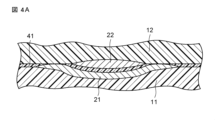
- FIG. 4A and 4B are partial cross-sectional views showing the first board-side wiring 21, the second board-side wiring 22, and the conductive member 41.
- FIG. 4A in a cross section perpendicular to the direction in which the first substrate-side wiring 21 extends at the portion where the first substrate-side wiring 21 and the second substrate-side wiring 22 overlap, the first substrate-side wiring 21
- the width of the second board-side wiring 22 is different from the width of the second board-side wiring 22
- the width of the second board-side wiring 22 is narrower than the width of the first board-side wiring 21 .
- the conductive member 41 is not between the first board-side wiring 21 and the second board-side wiring 22 . Therefore, the first substrate-side wiring 21 and the second substrate-side wiring 22 can be electrically connected more reliably.
- the conductive member 41 When electrically connecting the first substrate-side wiring 21 and the second substrate-side wiring 22 via the conductive member 41, the conductive member 41 is arranged between the first substrate-side wiring 21 and the second substrate-side wiring 22. Then, while applying pressure in a direction orthogonal to the first principal surface, the bonding is performed by thermocompression. At that time, as shown in FIG. 4B, if the width of the first substrate-side wiring 21 and the width of the second substrate-side wiring 22 are the same, the first substrate-side wiring 21 and the second substrate-side wiring 22 are not aligned. Contact occurs only at the edges, and doming tends to occur in which the conductive member 41 is confined in the central portion in the width direction. When doming occurs, the thickness in the direction perpendicular to the first main surface 111 at the widthwise central portion of the connecting portion between the first substrate-side wiring 21 and the second substrate-side wiring increases. Therefore, electrical connection via the conductive member 41 cannot be sufficiently performed.
- the width of the first board-side wiring 21 and the width of the second board-side wiring 22 are different, so that the conductive member 41 is not confined and spreads evenly even during thermocompression bonding. becomes.
- the first board-side wiring 21 and the second board-side wiring 22 are electrically connected more reliably.
- the width of the first substrate-side wiring 21 and the width of the second substrate-side wiring 22 are different, and one wiring has a wider width than the other wiring. can be lowered further.
- misalignment can be reduced, and the yield can be increased.
- the width direction refers to a direction perpendicular to the direction in which the first board-side wiring 21 extends along the first main surface 111 .
- the side edge of the wiring refers to an edge along the direction in which the wiring extends.
- a cross section perpendicular to the direction in which the first board-side wiring 21 extends at the portion where the first board-side wiring 21 and the second board-side wiring 22 overlap is the first board-side wiring 21 and the second board-side wiring 22 . 22 is a cross-sectional view of the central portion in the direction in which the first board-side wiring 21 extends.
- the shortest distance d1 between adjacent first substrate-side wirings 21 is less than 250 ⁇ m, and the shortest distance d2 between adjacent second substrate-side wirings 22 is 250 ⁇ m or more.
- the narrower width is preferably 500 ⁇ m or less, and may be 300 ⁇ m or less.
- the width of the second board-side wiring 22 is narrower than the width of the first board-side wiring 21 , but the width of the first board-side wiring 21 is narrower than the width of the first board-side wiring 22 . It can be narrow.
- the first electronic component 31 has, for example, connectors, elements, and control circuits.
- the first electronic component 31 is arranged only on the first main surface 111 and is electrically connected to the plurality of first substrate wirings 21 . As a result, the electronic components are provided only on the first substrate, which makes it easier to lower the difficulty of manufacturing the second substrate.
- the first board-side wiring 21 and the electronic component 31 are electrically connected via mounting electrodes 42 and solder 43 .
- the electronic component 31 has terminals (not shown). Specifically, the ends of the first board-side wirings 21 are covered with mounting electrodes 42 , and the electronic component 31 is electrically connected to the mounting electrodes 42 via solder 43 .
- a mixture of metal powder such as silver or copper and thermosetting resin such as epoxy resin is used for the mounting electrodes 42 .
- the width of the second board-side wiring 22 is , the width of the first substrate-side wiring 21 is narrower, but not limited thereto, and the width of the first substrate-side wiring 21 may be narrower than the width of the second substrate-side wiring 22 .
- the first substrate-side wiring 21 and the second substrate-side wiring 22 are electrically connected via the conductive member 41.
- the present invention is not limited to this, and the first substrate-side wiring and the second substrate can be connected.
- the side wiring may be electrically connected by direct contact between the first substrate side wiring and the third substrate side wiring.
- FIG. 5 is a plan view showing a second embodiment of an elastic device.
- the second embodiment differs from the first embodiment in that it further includes a third substrate and third substrate-side wiring arranged on the third substrate.
- This different configuration is described below. The rest of the configuration is the same as that of the first embodiment, and the same reference numerals as those of the first embodiment are given, and the description thereof is omitted.
- the second substrate 12A further has an edge 12b, the third substrate 13, and a plurality of third substrates provided on the third substrate 13.
- a side wiring 23 and a third electronic component 33 are provided.
- One of the adjacent third substrate side wirings corresponds to the sixth wiring described in the claims, and the other corresponds to the seventh wiring described in the claims. This makes it possible to manufacture elastic devices with more complicated configurations.
- the third substrate 13 is made of a resin material such as epoxy resin, urethane resin, acrylic resin, silicone resin, phenol resin, or polyimide resin, and may contain glass fiber or paper fiber.
- the expansion ratio of the third substrate 13 is preferably 100-1000%. Complicated wiring on the third substrate 13 can be easily formed by setting the expansion ratio as described above.
- the Young's modulus of the third substrate 13 is preferably 0.1-50 MPa. By setting the Young's modulus as described above, it is easy to form complicated wiring on the third substrate 13 .
- the thickness of the third substrate 13 is, for example, 10-100 ⁇ m.
- the third substrate 13 includes a fifth main surface 131 and a sixth main surface 132 facing each other.
- the third substrate 13 is formed in a rectangular shape in plan view, and is arranged so that one edge 13a of the third substrate 13 faces the edge 12b of the second substrate 12 .
- the third substrate-side wiring 23 is made of a conductive material.
- a conductive material for example, a foil of a metal such as silver or copper may be used, or a mixture of a powder of a metal such as silver or copper and an elastomeric resin such as silicone may be used.
- a mixture of an elastomeric resin such as an epoxy resin, a urethane resin, an acrylic resin, or a silicone resin may also be used.
- the thickness of the metal foil is preferably 0.01 ⁇ m or more and 10 ⁇ m or less, and the average particle size D50 of the metal powder is preferably 0.01 ⁇ m or more and 10 ⁇ m or less.
- the shape of the metal powder may be a spherical shape, a flat shape, an irregular shape having projections, or the like.
- the third board-side wiring 23 may be stretchable.
- the thickness of the third substrate wiring 23 is preferably 100 ⁇ m or less, more preferably 50 ⁇ m or less, and preferably 1 ⁇ m or more, more preferably 10 ⁇ m or more. As the thickness of the third substrate-side wiring 23 is thinner, the unevenness is smaller and the lamination or the like is easier.
- the width of the third substrate wiring 23 is preferably 100 ⁇ m or more and 10,000 ⁇ m or less, more preferably 300 ⁇ m or more and 4,000 ⁇ m or less.
- the third board-side wiring 23 is arranged on the fifth main surface 131 . That is, both the sixth wiring and the seventh wiring described in the claims are arranged on the fifth main surface 131 and exist on the same main surface.
- the third substrate-side wiring 23 is formed by screen printing, inkjet printing, dispensing, or etching of metal foil so as to be in direct contact with the fifth main surface 131 .
- the third substrate-side wiring 23 may be arranged on the fifth main surface 131 via another member such as an insulating member (not shown). Also, the third substrate-side wiring 23 may be covered with an insulating coating layer (not shown).
- the third board-side wiring 23 includes a third area overlapping the third electronic component 33 or the terminals of the third electronic component 33 when viewed from the direction perpendicular to the fifth board 131, 3 and a fourth region that does not overlap the terminals of the electronic component 33 .
- the shortest distance between the sixth wiring and the seventh wiring described in the claims means the shortest distance between the fourth regions of each wiring.
- a plurality of third substrate-side wirings 23 extend along the fifth main surface 131 .
- the plurality of third substrate-side wirings may be spaced apart from each other without intersecting each other. It extends along the fifth major surface 131 .
- the third board-side wirings 23 are electrically connected to the second board-side wirings 22 respectively.
- the third board-side wiring 23 corresponding to the sixth wiring may be electrically connected to the second board-side wiring corresponding to the third wiring, and the second board-side wiring 23 corresponding to the seventh wiring may be electrically connected to It may be electrically connected to the second board side wiring 22 corresponding to the fourth wiring.
- the third board-side wiring 23 is composed of a straight portion and a corner portion, but is not limited to this, and may have a curved portion.
- the shortest distance d3 between adjacent third board-side wirings 23 is shorter than the shortest distance d2 between adjacent second board-side wirings 22 . That is, the wiring pattern arranged on the fifth principal surface 131 is finer than the wiring pattern arranged on the fourth principal surface 122 . Therefore, while fine wiring patterns are formed on the third substrate 13, the wirings are arranged relatively sparsely and dispersedly on the stretchable second substrate 12. FIG. Therefore, manufacturing difficulty is not high, and manufacturing can be performed with a high yield. Furthermore, since the wiring is arranged relatively sparsely distributed on the second substrate 12, the expansion and contraction load can be relatively evenly absorbed by the entire second substrate 12. FIG.
- the shortest distance d3 between the third board-side wirings 23 is obtained by sequentially measuring the distance from one third board-side wiring 23a to the other first board-side wiring 23b along one third board-side wiring 23a. The shortest value among the obtained measurement values.
- the shortest distance d3 between the adjacent third board-side wirings 23 is shorter than the shortest distance d2 between the adjacent second board-side wirings 22 means that d3 has a smaller value when d3 and d2 are compared.
- predetermined second substrate-side wirings are 22a, 22b, 22c, and 22d
- predetermined third substrate-side wirings are 23a, 23b, 23c, and 23d.
- the shortest distance between adjacent third board side wirings 23 is the smallest value among the shortest distances of n ⁇ 1 pairs of adjacent third board side wirings 23 .
- the shortest distance between the first set of adjacent third board side wirings 23a and 23b is d31
- the shortest distance between the second set of adjacent third board side wirings 23c and 23d is d32. Comparing the shortest distance d31 and the shortest distance d32, the shortest distance d31 is smaller. Thus, by obtaining n ⁇ 1 shortest distances and comparing these values, the shortest distance d3, which is the minimum value, can be obtained.
- the shortest distance between the adjacent third board-side wirings 23 is shorter than the shortest distance between the adjacent second board-side wirings 22 means that d3 has a smaller value when d3 and d2 are compared. .
- the third electronic component 33 has, for example, connectors, elements, and control circuits.
- the third electronic component 33 is arranged on the fifth main surface 131 and electrically connected to the plurality of third board-side wirings 23 . Since other effects of the configuration are the same as those of the first embodiment, description thereof will be omitted.
- FIGS. 6A and 6B show a third embodiment of the stretchable device, and are enlarged plan views showing the first substrate-side wiring and the second substrate-side wiring.
- the third embodiment differs from the first embodiment in the configuration of the first substrate-side wiring and the second substrate-side wiring. This different configuration is described below. The rest of the configuration is the same as that of the first embodiment, and the same reference numerals as those of the first embodiment are given, and the description thereof is omitted.
- At least one of the first substrate-side wiring 21B and the second substrate-side wiring 22B has a comb-shaped end, and preferably the second substrate-side wiring 22B has comb-teeth. with rounded ends.
- the conductive member can flow out between the teeth of the first substrate. Since it is not confined between the side wiring 21B and the second substrate side wiring 22B, doming is suppressed and the electrical connection between the first substrate side wiring 21B and the second substrate side wiring 22B is improved.
- the comb tooth-shaped end has a plurality of teeth 22a that are arranged in parallel in the width direction and are spaced apart. be.
- the area of the portion where the first board-side wiring 21B and the second board-side wiring 22B overlap increases, so that the first board-side wiring 21B and the second board-side wiring 22B are electrically connected more reliably.
- the interval between two adjacent tooth portions 22a is preferably 200 ⁇ m or more in all tooth portions 22a.
- the interval between two adjacent tooth portions 22a is the same for all tooth portions.
- the plurality of tooth portions are arranged at equal intervals in the width direction, so that the first wiring and the third wiring are electrically connected more reliably.
- the interval between two adjacent tooth portions 22a may be 0.5 to 2 times the width of the tooth portion, or may be 0.8 to 1.2 times the width of the tooth portion.
- At least a portion of the tooth portion 22a may overlap the first substrate-side wiring 21B, and the entire tooth portion 22a may overlap the first substrate-side wiring 21B.
- the second substrate-side wiring 22B has a comb-shaped end, but the present invention is not limited to this. may have an end of In this case, the number of teeth provided at the end of the second board-side wiring 22B and the number of teeth provided at the end of the first board-side wiring 21B connected to the second board-side wiring 22B are They may be the same or different.
- the number of teeth provided at the end of the second board-side wiring 22B is twice the number of teeth provided at the end of the first board-side wiring 21B connected to the second board-side wiring 22B. good too. For example, as shown in FIG.
- the number of teeth provided at the end of the second board-side wiring 22B is four, and the end of the first board-side wiring 21B connected to the second board-side wiring 22B is The number of teeth provided in may be two.
- the number of teeth provided at the end of the second board-side wiring 22B is half the number of teeth provided at the end of the first board-side wiring 21B connected to the second board-side wiring 22B.
- the number of tooth portions provided at the end of the second board-side wiring 22B is two, and the tooth is provided at the end of the first board-side wiring 21B connected to the second board-side wiring 22B.
- the number of teeth provided may be four.
- the number of teeth provided at the end of the comb tooth shape is two or four, but the number is not limited to this, and the number can be freely increased or decreased. Since other effects of the configuration are the same as those of the first embodiment, description thereof will be omitted.
- FIG. 7 shows a fourth embodiment of the stretchable device, and is an enlarged plan view showing the first substrate-side wiring and the fifth wiring.
- FIG. 8 is a sectional view taken along line II-II of FIG.
- the fourth embodiment differs from the first embodiment in that it has a fifth wiring. This different configuration is described below. The rest of the configuration is the same as that of the first embodiment, and the same reference numerals as those of the first embodiment are given, and the description thereof is omitted.
- the stretchable device 1C of the fourth embodiment further comprises a fifth wiring 27 provided on the first main surface 111C, and the fifth wiring 27 extends on the first main surface 111C. It has a region that overlaps with the first substrate-side wiring 21C when viewed from the orthogonal direction. In other words, the overlap of the wirings arranged on the first substrate 11C in the direction orthogonal to the first main surface 111C is greater than the overlap of the wirings arranged on the second substrate 12C in the direction orthogonal to the fourth main surface 122. lower. As a result, a more complicated wiring pattern is arranged on the first substrate 11, the wiring pattern on the second substrate 12 can be simplified, and the manufacturing difficulty of the second substrate can be lowered.
- the fifth wiring 27 is made of a conductive material.
- a metal foil of silver, copper, nickel, or the like may be used.
- a mixture consisting of The thickness of the metal foil is preferably 0.01 ⁇ m or more and 10 ⁇ m or less, and the average particle size D50 of the metal powder is preferably 0.01 ⁇ m or more and 10 ⁇ m or less.
- the shape of the metal powder may be a spherical shape, a flat shape, an irregular shape having projections, or the like.
- the fifth wiring 27 may be stretchable. If the fifth wiring 27 is expandable and contractible, even when the fifth wiring is formed on the wiring on the first substrate side, disconnection or the like can be easily suppressed.
- the thickness of the fifth wiring 27 is preferably 100 ⁇ m or less, more preferably 50 ⁇ m or less, and preferably 1 ⁇ m or more, more preferably 10 ⁇ m or more.
- the width of the fifth wiring 27 is preferably 100 ⁇ m or more and 10,000 ⁇ m or less, more preferably 300 ⁇ m or more and 4,000 ⁇ m or less.
- the fifth wiring 27 is arranged on the first main surface 111C.
- the fifth wiring 27 is formed on the first main surface 111C by screen printing, inkjet printing, dispensing, or etching of metal foil.
- the fifth wiring 27 and the first substrate-side wiring 21C are electrically insulated by an insulating member 51C. Also, the fifth wiring 27 may be covered with an insulating coating layer (not shown).
- the fifth wiring 27 intersects the first substrate wiring 21C when viewed from the direction perpendicular to the first main surface 111C.
- the fifth wiring 27 and the first substrate-side wiring 21C are orthogonal to each other, but the invention is not limited to this, and the crossing angle can be freely increased or decreased.
- the seventh board-side wiring is composed of a straight portion, but is not limited to this, and may have a corner portion and a curved portion.
- FIG. 7 shows only the fifth wiring 27 and the first substrate-side wiring 21C, it is not limited to this.
- eighth wirings are electrically connected to the fifth wirings 27, are arranged apart from each other without intersecting each other, and extend along the fourth main surface. may be placed.
- the configuration of the eighth wiring is the same as the configuration of the second substrate side wiring.
- a fourth electronic component electrically connected to the fifth wiring 27 may be arranged on the first main surface 111C.
- the configuration of the fourth electronic component is the same as that of the first electronic component. Since other effects of the configuration are the same as those of the first embodiment, description thereof will be omitted.
- FIG. 9 shows a fifth embodiment of the stretchable device, and is a partial cross-sectional view showing the first substrate-side wiring and the second substrate-side wiring.
- 5th Embodiment differs in the structure which has an insulating coating layer from 1st Embodiment. This different configuration is described below. The rest of the configuration is the same as that of the first embodiment, and the same reference numerals as those of the first embodiment are given, and the description thereof is omitted.
- the first substrate-side wiring 21D is formed on the first main surface 111D with the first insulating member 53 interposed therebetween. are covered with a first insulating covering layer 51 .
- the second board-side wiring 22D is formed on the fourth main surface 122D via the second insulating member 54, and the second board-side wiring 22D is covered with the second insulating cover layer 52.
- the first board-side wiring 21D, the second board-side wiring 22D, and the conductive member 41D are arranged so as to overlap each other in a direction perpendicular to the first main surface 111, and the first insulating coating layer 51 is arranged on the first main surface. It overlaps with the conductive member 41D when viewed from the direction orthogonal to 111D.
- the second insulating coating layer overlaps the conductive member 41D when viewed from the direction orthogonal to the fourth main surface 122D.
- the first board-side wiring 21D is covered with the first insulating coating layer 51, contact between the first board-side wiring 21D and the outside is suppressed, and noise can be reduced. Furthermore, the first insulating coating layer 51 has a region arranged between the second board-side wiring 22D and the conductive member 41D in the direction orthogonal to the first main surface 111D. Therefore, it becomes easier to suppress breakage of the first substrate-side wiring 21D. Further, since the second board-side wiring 22D is covered with the second insulating coating layer 52, contact between the second board-side wiring 22D and the outside is suppressed, and noise can be reduced.
- the second insulating coating layer 52 has a region arranged between the first board-side wiring 21D and the conductive member 41D in the direction perpendicular to the first main surface 111D. Therefore, it becomes easier to suppress breakage of the second substrate-side wiring 22D.
- the first substrate-side wiring 21D is formed on the first main surface 111D via the first insulating member 53, but is not limited to this, and is formed without the first insulating member 53.
- the second board-side wiring 22D is formed on the fourth main surface 122D with the second insulating member 54 interposed therebetween, but is not limited to this, and is formed without the second insulating member 54 interposed therebetween.
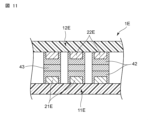
- FIG. 10 shows a sixth embodiment of the stretchable device, and is a cross-sectional view showing the first substrate-side wiring and the second substrate-side wiring.
- 11 is a cross-sectional view taken along line III-III of FIG. 10.
- FIG. The sixth embodiment differs from the first embodiment in that the first substrate-side wiring and the second substrate-side wiring are electrically connected via solder and mounting electrodes. This different configuration is described below. The rest of the configuration is the same as that of the first embodiment, and the same reference numerals as those of the first embodiment are given, and the description thereof is omitted.
- the first substrate-side wiring 21E and the second substrate-side wiring 22E are electrically connected via mounting electrodes 42 and solder 43. be done. Specifically, the ends of the first board-side wiring 21E and the second board-side wiring 22E are each covered with mounting electrodes 42, and the respective mounting electrodes 42 are electrically connected via solder 43. Connected. As a result, the electrical connection between the first board-side wiring 21E and the second board-side wiring 22E can be ensured, and it is possible to deal with various forms of manufacture of elastic devices.
- the first board-side wiring 21E and the second board-side wiring 22E are deformed at the time of soldering. Therefore, the first board-side wiring 21E and the second board-side wiring 22E can be electrically connected more reliably.
- a mixture of metal powder such as silver and copper and thermosetting resin such as epoxy resin is used for mounting electrodes. Since other effects of the configuration are the same as those of the first embodiment, description thereof will be omitted.
- the first substrate-side wiring and the second substrate-side wiring are electrically connected via the mounting electrodes and the solder, but the present invention is not limited to this.
- the side wiring may be electrically connected via a mounting electrode and a conductive adhesive.
- FIG. 12 is a cross-sectional view showing a seventh embodiment of an elastic device.
- the seventh embodiment differs from the second embodiment in the configuration of the second substrate and the configuration in which a connector is used instead of a conductive member for electrical connection between the first substrate-side wiring and the second substrate-side wiring.
- This different configuration is described below.
- the rest of the configuration is the same as that of the first embodiment, and the same reference numerals as those of the first embodiment are given, and the description thereof is omitted.
- the second substrate 12F is arranged such that the fourth main surface 122F faces the same direction as the first main surface 111F, and the first substrate side wiring 21F is arranged. and the second board-side wiring 22F are electrically connected via a connector 44. As shown in FIG. At the same time, the first substrate 11F and the second substrate 12F are connected via the connector 44. As shown in FIG. By electrically connecting the first board-side wiring 21 and the second board-side wiring 22F via the connector 44, the mechanical strength of the connection portion is increased.
- the first board-side wiring 21F and the second board-side wiring 22F are electrically connected via the connector 44.
- the second board-side wiring 22F and the third board-side wiring are may be electrically connected via Since other effects of the configuration are the same as those of the first embodiment, description thereof will be omitted.
- FIG. 13 is a plan view showing an eighth embodiment of an elastic device;
- the eighth embodiment differs from the first embodiment in that the second electronic component is provided on the second substrate.
- This different configuration is described below. The rest of the configuration is the same as that of the first embodiment, and the same reference numerals as those of the first embodiment are given, and the description thereof is omitted.
- a first electronic component 31G has a plurality of first component terminals 311, and a plurality of second terminal terminals 311 are formed on the fourth main surface 122G.
- a second electronic component 32 having component terminals 321 is arranged.
- One of the adjacent first electronic component terminals 311 corresponds to the first terminal, and the other corresponds to the second terminal.
- one of the adjacent second electronic component terminals corresponds to the third terminal, and the other corresponds to the fourth terminal.
- the first component terminals 311 are electrically connected to the first substrate wirings 21G, respectively.
- the first component terminal 311 corresponding to the first terminal is electrically connected to the first board side wiring 21G corresponding to the first wiring, and the first component terminal 311 corresponding to the second terminal corresponds to the second wiring. is electrically connected to the first board-side wiring 21G.
- the second electronic component 32 has, for example, connectors, elements, and control circuits.
- the second electronic component 32 is arranged on the fourth main surface 122G.
- the second component terminals 321 are electrically connected to the second board wirings 22G.
- the second component terminal 321 corresponding to the third terminal is electrically connected to the second board side wiring 22G corresponding to the third wiring, and the second component terminal 322 corresponding to the fourth terminal corresponds to the fourth wiring. is electrically connected to the second board-side wiring 22G.
- the shortest distance d3 between adjacent first component terminals is shorter than the shortest distance d4 between adjacent second component terminals. That is, the electronic component provided on the first substrate has a narrower inter-terminal distance than the electronic component provided on the second component. As a result, even when the second electronic component is also provided on the stretchable second substrate, the shortest distance between the first terminal and the second terminal in the first electronic component on the first substrate is the second substrate. Since the shortest distance between the third terminal and the fourth terminal in the upper second electronic component is shorter than the shortest distance, the wiring is arranged in a relatively sparsely distributed manner on the second substrate, thereby reducing manufacturing difficulty. becomes easier.
- the first component terminals 311 and the second component terminals 321 are arranged on the side surface of the electronic component, respectively, but are not limited to this, and may be arranged on the bottom surface of the electronic component. Since other effects of the configuration are the same as those of the first embodiment, description thereof will be omitted.
- FIG. 14 is a plan view showing a ninth embodiment of the elastic device.
- the ninth embodiment differs from the first embodiment in that the width of the first substrate-side wiring is wider than the width of the second substrate-side wiring.
- the width of the first substrate-side wiring 21H is wider than the width of the second substrate-side wiring 22H. Since the width of the first board-side wiring 21H is wide, deformation of the board can be suppressed and connection reliability can be improved.
- the thickness of the second substrate wiring 22H is preferably 100 ⁇ m or less, more preferably 50 ⁇ m or less, and preferably 1 ⁇ m or more, more preferably 10 ⁇ m or more. As the thickness of the first substrate-side wiring 21 is thinner, unevenness is smaller and lamination or the like is easier.
- the width of the first substrate wiring 21 is preferably 100 ⁇ m or more and 10,000 ⁇ m or less, more preferably 300 ⁇ m or more and 4,000 ⁇ m or less. In FIG. 14, the edges of the ends of the first board-side wiring 21H and the second board-side wiring 22H are linear, but the invention is not limited to this.
- At least one of the first substrate-side wiring 21H and the second substrate-side wiring 22H may have a comb-shaped end, preferably the first substrate-side wiring 21H. may have pectinate ends.
- the conductive member can flow out between the comb teeth and the first substrate. Since it is not confined between the side wiring 21H and the second substrate side wiring 22I, doming is suppressed and the electrical connection between the first substrate side wiring 21H and the second substrate side wiring 22H is improved.
- the comb tooth-shaped end portion has a plurality of teeth 21e that are arranged in parallel in the width direction and are spaced apart. be.
- the area of the portion where the first board-side wiring 21I and the second board-side wiring 22I overlap increases, so that the first board-side wiring 21I and the second board-side wiring 22I are electrically connected more reliably.
- the interval between two adjacent tooth portions 21e is preferably 200 ⁇ m or more in all tooth portions 21e.
- the interval between two adjacent tooth portions 21e is the same for all tooth portions.
- the plurality of tooth portions are arranged at equal intervals in the width direction, so that the first wiring and the third wiring are electrically connected more reliably.
- the interval between two adjacent tooth portions 21e may be 0.5 to 2 times the width of the tooth portion, or may be 0.8 to 1.2 times the width of the tooth portion.
- At least a portion of the tooth portion 21e may overlap the second substrate wiring 22H, and the entire tooth portion 21e may overlap the second substrate wiring 22H.
- the first substrate-side wiring 21H has a comb-shaped end, but the present invention is not limited to this. may have an end of In this case, the number of teeth provided at the end of the first board-side wiring 21H and the number of teeth provided at the end of the second board-side wiring 22H connected to the first board-side wiring are the same. may be different.
- the number of teeth provided at the end of the first board-side wiring 21H is twice the number of teeth provided at the end of the second board-side wiring 22H connected to the first board-side wiring 21H. good too. For example, as shown in FIG.
- the number of teeth provided at the end of the first board-side wiring 21H is four, and the end of the second board-side wiring 22H connected to the first board-side wiring 21H is The number of teeth provided in may be two.
- the number of teeth provided at the end of the first board-side wiring 21H is half the number of teeth provided at the end of the second board-side wiring 22H connected to the first board-side wiring 21H.
- the number of teeth provided at the end of the first board-side wiring 21H is two, and the tooth is provided at the end of the second board-side wiring 22H connected to the first board-side wiring 21H.
- the number of teeth provided may be four. Also, in FIG.
- the number of teeth provided at the end of the comb tooth is two or four, but the number is not limited to this, and the number can be freely increased or decreased. Since other effects of the configuration are the same as those of the first embodiment, description thereof will be omitted.
- the width of the first substrate-side wiring is narrower than the width of the second substrate-side wiring
- the width of the first substrate-side wiring is wider than the width of the second substrate-side wiring.
- the first substrate-side wiring may include a wiring that is wider than the second substrate-side wiring and a wiring that is narrower than the second substrate-side wiring.
- the width of the first substrate-side wiring and the width of the second substrate-side wiring may be the same.
- the first substrate has a rectangular shape in the above embodiment, it is not limited to a rectangular shape and may have, for example, a polygonal shape.
- the polygonal shape may be an outwardly convex polygonal shape or an inwardly concave polygonal shape.
- the second substrate has a rectangular shape in the above embodiment, it is not limited to a rectangular shape, and may have, for example, a non-long shape such as a polygon, a circle, or an ellipse.
- the third substrate has a rectangular shape in the above embodiment, it is not limited to a rectangular shape and may have, for example, a polygonal shape.
- the polygonal shape may be an outwardly convex polygonal shape or an inwardly concave polygonal shape.
- the first electronic component is arranged on the first main surface in the above embodiment, it is not limited to being arranged on the first main surface, and may be arranged on the second main surface, for example.
- the second electronic component is arranged on the fourth main surface in the above embodiment, it is not limited to being arranged on the fourth main surface, and may be arranged on the third main surface.
Landscapes
- Engineering & Computer Science (AREA)
- Microelectronics & Electronic Packaging (AREA)
- Structure Of Printed Boards (AREA)
- Combinations Of Printed Boards (AREA)
- Physics & Mathematics (AREA)
- Geometry (AREA)
Priority Applications (2)
| Application Number | Priority Date | Filing Date | Title |
|---|---|---|---|
| JP2023566194A JP7540611B2 (ja) | 2021-12-10 | 2022-11-15 | 伸縮デバイス |
| US18/734,031 US20240321721A1 (en) | 2021-12-10 | 2024-06-05 | Stretchable device |
Applications Claiming Priority (2)
| Application Number | Priority Date | Filing Date | Title |
|---|---|---|---|
| JP2021-201035 | 2021-12-10 | ||
| JP2021201035 | 2021-12-10 |
Related Child Applications (1)
| Application Number | Title | Priority Date | Filing Date |
|---|---|---|---|
| US18/734,031 Continuation US20240321721A1 (en) | 2021-12-10 | 2024-06-05 | Stretchable device |
Publications (1)
| Publication Number | Publication Date |
|---|---|
| WO2023106051A1 true WO2023106051A1 (ja) | 2023-06-15 |
Family
ID=86730402
Family Applications (1)
| Application Number | Title | Priority Date | Filing Date |
|---|---|---|---|
| PCT/JP2022/042423 Ceased WO2023106051A1 (ja) | 2021-12-10 | 2022-11-15 | 伸縮デバイス |
Country Status (3)
| Country | Link |
|---|---|
| US (1) | US20240321721A1 (https=) |
| JP (1) | JP7540611B2 (https=) |
| WO (1) | WO2023106051A1 (https=) |
Citations (5)
| Publication number | Priority date | Publication date | Assignee | Title |
|---|---|---|---|---|
| JPS56172980U (https=) * | 1980-05-21 | 1981-12-21 | ||
| JP2011034822A (ja) * | 2009-08-03 | 2011-02-17 | Tokai Rubber Ind Ltd | 配線体接続構造体およびその製造方法 |
| JP2016178121A (ja) * | 2015-03-18 | 2016-10-06 | タツタ電線株式会社 | ストレッチャブルケーブルおよびストレッチャブル回路基板 |
| WO2019138855A1 (ja) * | 2018-01-15 | 2019-07-18 | パイクリスタル株式会社 | フレキシブル基板、電子デバイス、電子デバイスの製造方法 |
| WO2020137078A1 (ja) * | 2018-12-27 | 2020-07-02 | 株式会社村田製作所 | 伸縮性配線基板 |
Family Cites Families (1)
| Publication number | Priority date | Publication date | Assignee | Title |
|---|---|---|---|---|
| JP6488189B2 (ja) * | 2015-05-18 | 2019-03-20 | 日本メクトロン株式会社 | 伸縮性配線基板 |
-
2022
- 2022-11-15 JP JP2023566194A patent/JP7540611B2/ja active Active
- 2022-11-15 WO PCT/JP2022/042423 patent/WO2023106051A1/ja not_active Ceased
-
2024
- 2024-06-05 US US18/734,031 patent/US20240321721A1/en active Pending
Patent Citations (5)
| Publication number | Priority date | Publication date | Assignee | Title |
|---|---|---|---|---|
| JPS56172980U (https=) * | 1980-05-21 | 1981-12-21 | ||
| JP2011034822A (ja) * | 2009-08-03 | 2011-02-17 | Tokai Rubber Ind Ltd | 配線体接続構造体およびその製造方法 |
| JP2016178121A (ja) * | 2015-03-18 | 2016-10-06 | タツタ電線株式会社 | ストレッチャブルケーブルおよびストレッチャブル回路基板 |
| WO2019138855A1 (ja) * | 2018-01-15 | 2019-07-18 | パイクリスタル株式会社 | フレキシブル基板、電子デバイス、電子デバイスの製造方法 |
| WO2020137078A1 (ja) * | 2018-12-27 | 2020-07-02 | 株式会社村田製作所 | 伸縮性配線基板 |
Also Published As
| Publication number | Publication date |
|---|---|
| US20240321721A1 (en) | 2024-09-26 |
| JP7540611B2 (ja) | 2024-08-27 |
| JPWO2023106051A1 (https=) | 2023-06-15 |
Similar Documents
| Publication | Publication Date | Title |
|---|---|---|
| US10575399B2 (en) | Multilayer substrate | |
| KR100896248B1 (ko) | 프린트 배선판의 접속 구조체 | |
| JP4068628B2 (ja) | 配線基板、半導体装置および表示モジュール | |
| US20160352031A1 (en) | Connection device | |
| US9136212B2 (en) | Circuit board | |
| JP2004193223A (ja) | 半導体装置 | |
| US10756462B2 (en) | Resin multilayer substrate and an electronic device and a joint structure of a resin multilayer substrate | |
| CN101828310B (zh) | 连接端子、半导体封装、布线基板、连接器及微接触器 | |
| US7425766B2 (en) | Film substrate, fabrication method thereof, and image display substrate | |
| KR101139084B1 (ko) | 다층 프린트 기판 및 그 제조 방법 | |
| US10993329B2 (en) | Board joint structure | |
| US10128588B2 (en) | Cable connecting structure | |
| JP4740708B2 (ja) | 配線基板、及び半導体装置 | |
| CN105409333B (zh) | 挠性印刷基板 | |
| WO2023106051A1 (ja) | 伸縮デバイス | |
| KR20060046302A (ko) | 반도체 장치 | |
| JP2009295857A (ja) | Icチップと外部配線との接続構造およびicチップ | |
| JP2007258410A (ja) | 配線基板接続構造体及びその製造方法 | |
| TWI726427B (zh) | 元件基板 | |
| JP4488073B2 (ja) | 電気接続装置 | |
| CN114242304B (zh) | 一种导电胶及其制作方法、显示装置 | |
| WO2017150060A1 (ja) | 実装構造及びモジュール | |
| CN208016129U (zh) | 树脂电路基板、部件搭载树脂电路基板 | |
| US12341233B2 (en) | Signal transmission line | |
| KR100852371B1 (ko) | 이방성 도전성 접착 필름을 갖는 디스플레이 디바이스 |
Legal Events
| Date | Code | Title | Description |
|---|---|---|---|
| 121 | Ep: the epo has been informed by wipo that ep was designated in this application |
Ref document number: 22903982 Country of ref document: EP Kind code of ref document: A1 |
|
| ENP | Entry into the national phase |
Ref document number: 2023566194 Country of ref document: JP Kind code of ref document: A |
|
| NENP | Non-entry into the national phase |
Ref country code: DE |
|
| 122 | Ep: pct application non-entry in european phase |
Ref document number: 22903982 Country of ref document: EP Kind code of ref document: A1 |