WO2023100807A1 - 絶縁チップおよび信号伝達装置 - Google Patents
絶縁チップおよび信号伝達装置 Download PDFInfo
- Publication number
- WO2023100807A1 WO2023100807A1 PCT/JP2022/043765 JP2022043765W WO2023100807A1 WO 2023100807 A1 WO2023100807 A1 WO 2023100807A1 JP 2022043765 W JP2022043765 W JP 2022043765W WO 2023100807 A1 WO2023100807 A1 WO 2023100807A1
- Authority
- WO
- WIPO (PCT)
- Prior art keywords
- electrode plate
- electrode
- chip
- insulating
- insulating layer
- Prior art date
- Legal status (The legal status is an assumption and is not a legal conclusion. Google has not performed a legal analysis and makes no representation as to the accuracy of the status listed.)
- Ceased
Links
Images




Classifications
-
- H—ELECTRICITY
- H10—SEMICONDUCTOR DEVICES; ELECTRIC SOLID-STATE DEVICES NOT OTHERWISE PROVIDED FOR
- H10D—INORGANIC ELECTRIC SEMICONDUCTOR DEVICES
- H10D84/00—Integrated devices formed in or on semiconductor substrates that comprise only semiconducting layers, e.g. on Si wafers or on GaAs-on-Si wafers
-
- H—ELECTRICITY
- H10—SEMICONDUCTOR DEVICES; ELECTRIC SOLID-STATE DEVICES NOT OTHERWISE PROVIDED FOR
- H10D—INORGANIC ELECTRIC SEMICONDUCTOR DEVICES
- H10D1/00—Resistors, capacitors or inductors
- H10D1/60—Capacitors
- H10D1/68—Capacitors having no potential barriers
- H10D1/692—Electrodes
-
- H—ELECTRICITY
- H01—ELECTRIC ELEMENTS
- H01G—CAPACITORS; CAPACITORS, RECTIFIERS, DETECTORS, SWITCHING DEVICES, LIGHT-SENSITIVE OR TEMPERATURE-SENSITIVE DEVICES OF THE ELECTROLYTIC TYPE
- H01G2/00—Details of capacitors not covered by a single one of groups H01G4/00-H01G11/00
- H01G2/10—Housing; Encapsulation
-
- H—ELECTRICITY
- H01—ELECTRIC ELEMENTS
- H01G—CAPACITORS; CAPACITORS, RECTIFIERS, DETECTORS, SWITCHING DEVICES, LIGHT-SENSITIVE OR TEMPERATURE-SENSITIVE DEVICES OF THE ELECTROLYTIC TYPE
- H01G4/00—Fixed capacitors; Processes of their manufacture
- H01G4/002—Details
- H01G4/228—Terminals
- H01G4/232—Terminals electrically connecting two or more layers of a stacked or rolled capacitor
-
- H—ELECTRICITY
- H01—ELECTRIC ELEMENTS
- H01G—CAPACITORS; CAPACITORS, RECTIFIERS, DETECTORS, SWITCHING DEVICES, LIGHT-SENSITIVE OR TEMPERATURE-SENSITIVE DEVICES OF THE ELECTROLYTIC TYPE
- H01G4/00—Fixed capacitors; Processes of their manufacture
- H01G4/33—Thin- or thick-film capacitors (thin- or thick-film circuits; capacitors without a potential-jump or surface barrier specially adapted for integrated circuits, details thereof, multistep manufacturing processes therefor)
-
- H—ELECTRICITY
- H01—ELECTRIC ELEMENTS
- H01G—CAPACITORS; CAPACITORS, RECTIFIERS, DETECTORS, SWITCHING DEVICES, LIGHT-SENSITIVE OR TEMPERATURE-SENSITIVE DEVICES OF THE ELECTROLYTIC TYPE
- H01G4/00—Fixed capacitors; Processes of their manufacture
- H01G4/38—Multiple capacitors, i.e. structural combinations of fixed capacitors
-
- H—ELECTRICITY
- H01—ELECTRIC ELEMENTS
- H01G—CAPACITORS; CAPACITORS, RECTIFIERS, DETECTORS, SWITCHING DEVICES, LIGHT-SENSITIVE OR TEMPERATURE-SENSITIVE DEVICES OF THE ELECTROLYTIC TYPE
- H01G4/00—Fixed capacitors; Processes of their manufacture
- H01G4/40—Structural combinations of fixed capacitors with other electric elements, the structure mainly consisting of a capacitor, e.g. RC combinations
-
- H—ELECTRICITY
- H10—SEMICONDUCTOR DEVICES; ELECTRIC SOLID-STATE DEVICES NOT OTHERWISE PROVIDED FOR
- H10W—GENERIC PACKAGES, INTERCONNECTIONS, CONNECTORS OR OTHER CONSTRUCTIONAL DETAILS OF DEVICES COVERED BY CLASS H10
- H10W20/00—Interconnections in chips, wafers or substrates
- H10W20/40—Interconnections external to wafers or substrates, e.g. back-end-of-line [BEOL] metallisations or vias connecting to gate electrodes
- H10W20/45—Interconnections external to wafers or substrates, e.g. back-end-of-line [BEOL] metallisations or vias connecting to gate electrodes characterised by their insulating parts
- H10W20/47—Interconnections external to wafers or substrates, e.g. back-end-of-line [BEOL] metallisations or vias connecting to gate electrodes characterised by their insulating parts comprising two or more dielectric layers having different properties, e.g. different dielectric constants
-
- H—ELECTRICITY
- H10—SEMICONDUCTOR DEVICES; ELECTRIC SOLID-STATE DEVICES NOT OTHERWISE PROVIDED FOR
- H10W—GENERIC PACKAGES, INTERCONNECTIONS, CONNECTORS OR OTHER CONSTRUCTIONAL DETAILS OF DEVICES COVERED BY CLASS H10
- H10W20/00—Interconnections in chips, wafers or substrates
- H10W20/40—Interconnections external to wafers or substrates, e.g. back-end-of-line [BEOL] metallisations or vias connecting to gate electrodes
- H10W20/495—Capacitive arrangements or effects of, or between wiring layers
- H10W20/496—Capacitor integral with wiring layers
-
- H—ELECTRICITY
- H10—SEMICONDUCTOR DEVICES; ELECTRIC SOLID-STATE DEVICES NOT OTHERWISE PROVIDED FOR
- H10W—GENERIC PACKAGES, INTERCONNECTIONS, CONNECTORS OR OTHER CONSTRUCTIONAL DETAILS OF DEVICES COVERED BY CLASS H10
- H10W42/00—Arrangements for protection of devices
-
- H—ELECTRICITY
- H10—SEMICONDUCTOR DEVICES; ELECTRIC SOLID-STATE DEVICES NOT OTHERWISE PROVIDED FOR
- H10W—GENERIC PACKAGES, INTERCONNECTIONS, CONNECTORS OR OTHER CONSTRUCTIONAL DETAILS OF DEVICES COVERED BY CLASS H10
- H10W44/00—Electrical arrangements for controlling or matching impedance
- H10W44/601—Capacitive arrangements
-
- H—ELECTRICITY
- H10—SEMICONDUCTOR DEVICES; ELECTRIC SOLID-STATE DEVICES NOT OTHERWISE PROVIDED FOR
- H10W—GENERIC PACKAGES, INTERCONNECTIONS, CONNECTORS OR OTHER CONSTRUCTIONAL DETAILS OF DEVICES COVERED BY CLASS H10
- H10W70/00—Package substrates; Interposers; Redistribution layers [RDL]
- H10W70/40—Leadframes
- H10W70/475—Capacitors in combination with leadframes
-
- H—ELECTRICITY
- H10—SEMICONDUCTOR DEVICES; ELECTRIC SOLID-STATE DEVICES NOT OTHERWISE PROVIDED FOR
- H10W—GENERIC PACKAGES, INTERCONNECTIONS, CONNECTORS OR OTHER CONSTRUCTIONAL DETAILS OF DEVICES COVERED BY CLASS H10
- H10W70/00—Package substrates; Interposers; Redistribution layers [RDL]
- H10W70/40—Leadframes
- H10W70/481—Leadframes for devices being provided for in groups H10D8/00 - H10D48/00
-
- H—ELECTRICITY
- H10—SEMICONDUCTOR DEVICES; ELECTRIC SOLID-STATE DEVICES NOT OTHERWISE PROVIDED FOR
- H10W—GENERIC PACKAGES, INTERCONNECTIONS, CONNECTORS OR OTHER CONSTRUCTIONAL DETAILS OF DEVICES COVERED BY CLASS H10
- H10W90/00—Package configurations
- H10W90/20—Configurations of stacked chips
- H10W90/293—Configurations of stacked chips characterised by non-galvanic coupling between the chips, e.g. capacitive coupling
-
- H—ELECTRICITY
- H10—SEMICONDUCTOR DEVICES; ELECTRIC SOLID-STATE DEVICES NOT OTHERWISE PROVIDED FOR
- H10W—GENERIC PACKAGES, INTERCONNECTIONS, CONNECTORS OR OTHER CONSTRUCTIONAL DETAILS OF DEVICES COVERED BY CLASS H10
- H10W90/00—Package configurations
- H10W90/701—Package configurations characterised by the relative positions of pads or connectors relative to package parts
-
- H—ELECTRICITY
- H10—SEMICONDUCTOR DEVICES; ELECTRIC SOLID-STATE DEVICES NOT OTHERWISE PROVIDED FOR
- H10W—GENERIC PACKAGES, INTERCONNECTIONS, CONNECTORS OR OTHER CONSTRUCTIONAL DETAILS OF DEVICES COVERED BY CLASS H10
- H10W90/00—Package configurations
- H10W90/811—Multiple chips on leadframes
-
- H—ELECTRICITY
- H10—SEMICONDUCTOR DEVICES; ELECTRIC SOLID-STATE DEVICES NOT OTHERWISE PROVIDED FOR
- H10W—GENERIC PACKAGES, INTERCONNECTIONS, CONNECTORS OR OTHER CONSTRUCTIONAL DETAILS OF DEVICES COVERED BY CLASS H10
- H10W72/00—Interconnections or connectors in packages
- H10W72/071—Connecting or disconnecting
- H10W72/075—Connecting or disconnecting of bond wires
-
- H—ELECTRICITY
- H10—SEMICONDUCTOR DEVICES; ELECTRIC SOLID-STATE DEVICES NOT OTHERWISE PROVIDED FOR
- H10W—GENERIC PACKAGES, INTERCONNECTIONS, CONNECTORS OR OTHER CONSTRUCTIONAL DETAILS OF DEVICES COVERED BY CLASS H10
- H10W90/00—Package configurations
- H10W90/701—Package configurations characterised by the relative positions of pads or connectors relative to package parts
- H10W90/731—Package configurations characterised by the relative positions of pads or connectors relative to package parts of die-attach connectors
- H10W90/734—Package configurations characterised by the relative positions of pads or connectors relative to package parts of die-attach connectors between a chip and a stacked insulating package substrate, interposer or RDL
-
- H—ELECTRICITY
- H10—SEMICONDUCTOR DEVICES; ELECTRIC SOLID-STATE DEVICES NOT OTHERWISE PROVIDED FOR
- H10W—GENERIC PACKAGES, INTERCONNECTIONS, CONNECTORS OR OTHER CONSTRUCTIONAL DETAILS OF DEVICES COVERED BY CLASS H10
- H10W90/00—Package configurations
- H10W90/701—Package configurations characterised by the relative positions of pads or connectors relative to package parts
- H10W90/751—Package configurations characterised by the relative positions of pads or connectors relative to package parts of bond wires
- H10W90/753—Package configurations characterised by the relative positions of pads or connectors relative to package parts of bond wires between laterally-adjacent chips
-
- H—ELECTRICITY
- H10—SEMICONDUCTOR DEVICES; ELECTRIC SOLID-STATE DEVICES NOT OTHERWISE PROVIDED FOR
- H10W—GENERIC PACKAGES, INTERCONNECTIONS, CONNECTORS OR OTHER CONSTRUCTIONAL DETAILS OF DEVICES COVERED BY CLASS H10
- H10W90/00—Package configurations
- H10W90/701—Package configurations characterised by the relative positions of pads or connectors relative to package parts
- H10W90/751—Package configurations characterised by the relative positions of pads or connectors relative to package parts of bond wires
- H10W90/759—Package configurations characterised by the relative positions of pads or connectors relative to package parts of bond wires between a chip and a laterally-adjacent discrete passive device
Definitions
- the present disclosure relates to insulating tips and signal transmission devices.
- an insulated gate driver that applies a gate voltage to the gate of a switching element such as a transistor is known (see Patent Document 1, for example).
- the gate driver has an insulating element such as a transformer or a capacitor that is used to insulate the primary side circuit and the secondary side circuit.
- a gate driver may be required to have an improved withstand voltage.
- Such a problem is not limited to the gate driver, but can similarly occur in a signal transmission device and an insulation chip that insulates the primary side circuit and the secondary side circuit and transmits a signal.
- An insulating chip for solving the above problems includes a substrate, an element insulating layer provided on the substrate, and a capacitor having a first electrode plate and a second electrode plate embedded in the element insulating layer, The first electrode plate and the second electrode plate are arranged to face each other in a first direction perpendicular to the thickness direction of the element insulating layer.
- a signal transmission device for solving the above problems is configured to perform at least one of transmission and reception of a signal to and from the first circuit through a first chip including a first circuit, an insulation chip, and the insulation chip.
- a second chip including a second circuit wherein the insulating chip includes a substrate, an element insulating layer provided on the substrate, and a first electrode plate and a second electrode plate embedded in the element insulating layer. and the first electrode plate and the second electrode plate are arranged to face each other in a first direction perpendicular to the thickness direction of the element insulating layer.
- the insulating chip and the signal transmission device it is possible to improve the withstand voltage.
- FIG. 1 is a circuit diagram schematically showing the circuit configuration in one embodiment of the signal transmission device.
- FIG. 2 is a cross-sectional view schematically showing the cross-sectional structure of the signal transmission device of FIG. 3 is a plan view schematically showing a planar structure of an insulating chip of the signal transmission device of FIG. 2.
- FIG. 4 is a cross-sectional view schematically showing the cross-sectional structure of the insulating chip of FIG. 3 taken along line F4-F4.
- FIG. 7 is a cross-sectional view schematically showing the cross-sectional structure of the insulating chip of FIG. 3 taken along line F7-F7.
- FIG. 8 is a cross-sectional view schematically showing the cross-sectional structure of the signal transmission device of the modification.
- FIG. 9 is a cross-sectional view schematically showing the cross-sectional structure of the insulating tip of the modification.
- FIG. 10 is a cross-sectional view schematically showing the cross-sectional structure of the insulating tip of the modification.
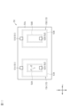
- FIG. 11 is a plan view schematically showing the planar structure of the insulating chip of the modified example.
- FIG. 12 is a plan view schematically showing the planar structure of the insulating chip of the modification.
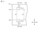
- FIG. 13 is a plan view schematically showing the planar structure of the insulating chip of the modification.
- FIG. 14 is a plan view schematically showing a planar structure of an insulating chip of a modified example.
- FIG. 1 shows a simplified example of the circuit configuration of the signal transmission device 10. As shown in FIG.
- the signal transmission device 10 is a device that transmits a pulse signal while electrically insulating a primary terminal 11 and a secondary terminal 12 from each other.
- the signal transfer device 10 is a digital isolator, an example of which is an AC/DC converter or gate driver or electronic components contained therein.
- the signal transmission device 10 includes a primary circuit 13 electrically connected to a primary terminal 11, a secondary circuit 14 electrically connected to a secondary terminal 12, and a primary circuit 13.
- a signal transmission circuit 10A having a capacitor 15 electrically connected to the secondary side circuit 14 is provided.
- the primary side circuit 13 corresponds to the "first circuit”
- the secondary side circuit 14 corresponds to the "second circuit”.
- the primary side circuit 13 is a circuit configured to operate when a first voltage is applied.
- the primary circuit 13 is electrically connected, for example, to an external control device (not shown).
- the secondary circuit 14 is a circuit configured to operate when a second voltage different from the first voltage is applied.
- the second voltage is higher than the first voltage, for example.
- the first voltage and the second voltage are DC voltages.
- Secondary circuit 14 is electrically connected to, for example, a drive circuit to be controlled by the control device.
- a drive circuit is a switching circuit.
- the signal transmission device 10 transmits the signal from the primary circuit 13 to the secondary circuit 14 via the capacitor 15 . is transmitted and a signal is output from the secondary side circuit 14 to the drive circuit via the secondary side terminal 12 .
- the signal transmission device 10 transmits a signal from a primary side circuit 13 to a secondary side circuit 14 via a capacitor 15 .
- the primary side circuit 13 and the secondary side circuit 14 are electrically insulated by the capacitor 15 . More specifically, while the capacitor 15 restricts the transmission of the DC voltage between the primary circuit 13 and the secondary circuit 14, it allows the transmission of the pulse signal.
- the state in which the primary side circuit 13 and the secondary side circuit 14 are insulated means the state in which the transmission of the DC voltage is interrupted between the primary side circuit 13 and the secondary side circuit 14. This means that the transmission of the pulse signal from the primary side circuit 13 to the secondary side circuit 14 is permitted.
- the secondary circuit 14 is configured to receive the signal of the primary circuit 13 .
- the dielectric strength of the signal transmission device 10 is, for example, 2500 Vrms or more and 7500 Vrms or less.
- the dielectric breakdown voltage of the signal transmission device 10 of this embodiment is about 5700 Vrms.
- the specific numerical value of the withstand voltage of the signal transmission device 10 is not limited to this and is arbitrary. Further, in this embodiment, as shown in FIG. 1, the ground of the primary circuit 13 and the ground of the secondary circuit 14 are provided independently.
- the signal transmission device 10 of this embodiment includes two capacitors 15 for transmitting two types of signals from the primary circuit 13 to the secondary circuit 14 . More specifically, the signal transmission device 10 includes a capacitor 15 used to transmit a first signal from the primary circuit 13 to the secondary circuit 14 and a second signal from the primary circuit 13 to the secondary circuit 14 . and a capacitor 15 used for transmitting two signals.
- the first signal is a signal containing rise information of the external signal input to the signal transmission device 10
- the second signal is a signal containing fall information of the external signal.
- a pulse signal is generated by the first signal and the second signal.
- capacitor 15A the capacitor 15 used for transmitting the first signal
- capacitor 15B the capacitor 15 used for transmitting the second signal
- the capacitor 15A corresponds to the "first signal capacitor”
- the capacitor 15B corresponds to the "second signal capacitor”.
- the signal transmission device 10 includes primary signal lines 16A, 16B and secondary signal lines 17A, 17B.
- the primary signal line 16A is a signal line that connects the primary circuit 13 and the capacitor 15A, and is a signal line that transmits the first signal from the primary circuit 13 to the capacitor 15A.
- the primary side signal line 16B is a signal line that connects the primary side circuit 13 and the capacitor 15B, and is a signal line that transmits the second signal from the primary side circuit 13 to the capacitor 15B.
- the secondary signal line 17A is a signal line that connects the capacitor 15A and the secondary circuit 14, and is a signal line that transmits the first signal from the capacitor 15A to the secondary circuit 14.
- the secondary signal line 17B is a signal line that connects the capacitor 15B and the secondary circuit 14, and is a signal line that transmits the second signal from the capacitor 15B to the secondary circuit 14.
- the first signal is transmitted from the primary circuit 13 to the secondary circuit 14 through the primary signal line 16A, the capacitor 15A, and the secondary signal line 17A in this order.
- the second signal is transmitted from primary circuit 13 to secondary circuit 14 via primary signal line 16B, capacitor 15B, and secondary signal line 17B in this order.
- the capacitor 15A transmits the first signal from the primary circuit 13 to the secondary circuit 14 and electrically insulates the primary circuit 13 and the secondary circuit 14 from each other.
- the capacitor 15A has a first electrode 21A and a second electrode 22A.
- the first electrode 21A is connected to the primary signal line 16A, and the second electrode 22A is connected to the secondary signal line 17A.
- the capacitor 15B transmits the second signal from the primary circuit 13 to the secondary circuit 14 and electrically insulates the primary circuit 13 and the secondary circuit 14 from each other.
- the capacitor 15B has a first electrode 21B and a second electrode 22B.
- the first electrode 21B is connected to the primary signal line 16B, and the second electrode 22B is connected to the secondary signal line 17B.
- the dielectric breakdown voltage of the capacitors 15A and 15B in this embodiment is, for example, 2500 Vrms or more and 7500 Vrms or less.
- the dielectric strength of the capacitors 15A and 15B may be 2500 Vrms or more and 5700 Vrms or less.
- the specific numerical value of the dielectric strength voltage of the capacitors 15A and 15B is not limited to this and is arbitrary.
- FIG. 2 shows an example of a cross-sectional structure schematically showing a part of the internal configuration of the signal transmission device 10.
- the signal transmission device 10 is a semiconductor device in which a plurality of semiconductor chips are packaged.
- the package format of the signal transmission device 10 is, for example, an SO (Small Outline) system, and in this embodiment, it is an SOP (Small Outline Package). Note that the package format of the signal transmission device 10 can be arbitrarily changed.
- the signal transmission device 10 includes a first chip 30, a second chip 40, and an insulating chip 50 as a plurality of semiconductor chips.
- the signal transmission device 10 also includes a primary die pad 60 on which the first chip 30 is mounted, a secondary die pad 70 on which the second chip 40 is mounted, the die pads 60 and 70 and the chips 30, 40, . and a sealing resin 80 that seals 50 .
- the primary die pad 60 corresponds to the "first mounting frame”
- the secondary die pad 70 corresponds to the "mounting frame” or the "second mounting frame”.
- the sealing resin 80 is made of an electrically insulating resin material, such as a black epoxy resin.
- the sealing resin 80 is formed in a rectangular plate shape having a thickness direction in the z direction.
- each die pad 60, 70 is made of a material containing Cu (copper).
- the die pads 60 and 70 may be made of other metal material such as Al (aluminum).
- the material forming each die pad 60, 70 is not limited to a conductive material.
- each die pad 60, 70 may be made of ceramics such as alumina. That is, each of the die pads 60 and 70 may be made of an electrically insulating material. The die pads 60 and 70 are not exposed from the sealing resin 80 in this embodiment.
- the primary die pad 60 and the secondary die pad 70 When viewed from the z-direction, the primary die pad 60 and the secondary die pad 70 are arranged side by side while being separated from each other.
- the arrangement direction of the primary die pads 60 and the secondary die pads 70 when viewed from the z direction is defined as the x direction.
- a direction perpendicular to the x direction when viewed from the z direction is the y direction.
- Both the primary die pad 60 and the secondary die pad 70 are formed in a flat plate shape.
- the x-direction length of the secondary die pad 70 is longer than the x-direction length of the primary die pad 60 .
- the insulating chip 50 is mounted on the secondary die pad 70 . That is, both the insulating chip 50 and the second chip 40 are mounted on the secondary die pad 70 .
- the second chip 40 and the insulating chip 50 are arranged apart from each other in the x direction. Therefore, the chips 30, 40, 50 are arranged apart from each other in the x-direction.
- the chips 30, 40, 50 are arranged in the order of the first chip 30, the insulating chip 50, and the second chip 40 from the primary die pad 60 toward the secondary die pad 70 in the x direction. ing. That is, the insulating chip 50 is arranged between the first chip 30 and the second chip 40 in the x direction.
- the distance between the primary die pad 60 and the secondary die pad 70 is greater than the distance between the second chip 40 and the insulating chip 50 in the x direction when viewed in the z direction. Therefore, when viewed from the z direction, the distance between the first tip 30 and the insulating tip 50 in the x direction is greater than the distance between the second tip 40 and the insulating tip 50 in the x direction. In other words, the insulating chip 50 is arranged closer to the second chip 40 than to the first chip 30 .
- the first chip 30 has a first substrate 33 on which the primary circuit 13 is formed.
- the first substrate 33 is, for example, a semiconductor substrate.
- An example of a semiconductor substrate is a substrate made of a material containing Si (silicon).
- a wiring layer 34 is formed on the first substrate 33 .
- the wiring layer 34 includes a plurality of insulating films stacked in the z-direction, metal layers provided between insulating films adjacent in the z-direction, and vias connecting metal layers positioned at different positions in the z-direction. have.
- the metal layers and vias constitute the wiring pattern of the first chip 30 .
- the metal layers and vias are electrically connected to, for example, primary circuit 13 .
- a protective film 35 is formed on the wiring layer 34 to protect the wiring layer 34 .
- the protective film 35 is made of an electrically insulating material.
- the first chip 30 has a chip front surface 30s and a chip rear surface 30r facing opposite sides in the z direction.
- the first substrate 33 constitutes the chip rear surface 30r
- the protective film 35 constitutes the chip front surface 30s.
- the chip back surface 30 r faces the primary die pad 60 .
- a plurality of first electrode pads 31 and a plurality of second electrode pads 32 are provided in a portion of the first chip 30 near the chip surface 30s. More specifically, each electrode pad 31, 32 is provided so as to be exposed from the chip surface 30s.
- a protective film 35 covers the electrode pads 31 and 32 .
- the protection film 35 has openings that expose the electrode pads 31 and 32 .
- Each of the electrode pads 31 and 32 is electrically connected to the primary circuit 13 by a wiring layer 34, for example.
- a plurality of first electrode pads 31 and a plurality of second electrode pads 32 are formed on the surface of the wiring layer 34 .
- the surface of the wiring layer 34 is the surface of the wiring layer 34 facing the same side as the chip surface 30s.
- the plurality of first electrode pads 31 are arranged on the opposite side of the chip surface 30s from the insulating chip 50 with respect to the center of the chip surface 30s in the x-direction.
- the plurality of electrode pads 31 are arranged apart from each other in the y direction.
- the plurality of second electrode pads 32 are arranged closer to the insulating chip 50 with respect to the center of the chip surface 30s in the x direction in the chip surface 30s.
- the plurality of second electrode pads 32 are arranged apart from each other in the y direction.
- the first chip 30 is bonded to the primary die pad 60 with the first bonding material 101.
- the first bonding material 101 is interposed between the chip back surface 30 r of the first chip 30 and the primary die pad 60 .
- the first bonding material 101 is a conductive bonding material such as solder paste or Ag (silver) paste.
- the primary circuit 13 is electrically connected to the primary die pad 60 via the first bonding material 101 .
- the primary die pad 60 constitutes a ground. Therefore, it can be said that the primary side circuit 13 is electrically connected to the ground.
- the material of the first bonding material 101 can be arbitrarily changed, and may be an insulating bonding material, for example.
- the primary side circuit 13 may be electrically connected to the primary side die pad 60 by a structure other than the first bonding material 101 (for example, a wire).
- the second chip 40 has a second substrate 43 on which the secondary circuit 14 is formed.
- the second substrate 43 is, for example, a semiconductor substrate.
- An example of a semiconductor substrate is a substrate made of a material containing Si.
- a wiring layer 44 is formed on the second substrate 43 .
- the wiring layer 44 includes insulating films stacked in the z-direction, metal layers provided between insulating films adjacent in the z-direction, and vias connecting metal layers positioned at different positions in the z-direction. ing.
- the metal layers and vias constitute the wiring pattern of the second chip 40 .
- the metal layers and vias are electrically connected to, for example, the secondary circuit 14 .
- a protective film 45 is formed on the wiring layer 44 to protect the wiring layer 44 .
- the protective film 45 is made of an electrically insulating material.
- the second chip 40 has a chip front surface 40s and a chip rear surface 40r facing opposite sides in the z direction.
- the second substrate 43 constitutes the chip rear surface 40r
- the protective film 45 constitutes the chip front surface 40s.
- the chip rear surface 40 r faces the secondary die pad 70 .
- the chip rear surface 40 r faces the same side as the chip rear surface 30 r of the first chip 30
- the chip front surface 40 s faces the same side as the chip front surface 30 s of the first chip 30 .
- a plurality of first electrode pads 41 and a plurality of second electrode pads 42 are provided in a portion of the second chip 40 near the chip surface 40s. More specifically, each electrode pad 41, 42 is provided so as to be exposed from the chip surface 40s.
- a protective film 45 covers the electrode pads 41 and 42 .
- the protective film 45 has openings that expose the electrode pads 41 and 42 .
- Each electrode pad 41 , 42 is electrically connected to the secondary circuit 14 by a wiring layer 44 , for example.
- a plurality of first electrode pads 41 and a plurality of second electrode pads 42 are formed on the surface of wiring layer 44 .
- the surface of the wiring layer 44 is the surface of the wiring layer 44 facing the same side as the chip surface 40s.
- the plurality of first electrode pads 41 are arranged closer to the insulating chip 50 with respect to the center of the chip surface 40s in the x direction than the chip surface 40s when viewed from the z direction. Although not shown, the plurality of first electrode pads 41 are arranged apart from each other in the y direction.
- the plurality of second electrode pads 42 are arranged on the opposite side of the chip surface 40s from the insulating chip 50 with respect to the center of the chip surface 40s in the x direction. Although not shown, the plurality of second electrode pads 42 are arranged apart from each other in the y direction.
- the second chip 40 is bonded to the secondary die pad 70 with the second bonding material 102 . More specifically, the second bonding material 102 is interposed between the chip rear surface 40 r and the secondary die pad 70 . The second bonding material 102 bonds the chip rear surface 40 r and the secondary die pad 70 .
- the second bonding material 102 is a conductive bonding material such as solder paste or Ag paste. In this embodiment, the second bonding material 102 is made of the same material as the first bonding material 101, for example.
- the material of the second bonding material 102 can be arbitrarily changed, and may be a conductive bonding material different from the material of the first bonding material 101, for example. Also, the second bonding material 102 may be an insulating bonding material. In this case, the secondary circuit 14 may be electrically connected to the secondary die pad 70 by means of a structure other than the second bonding material 102 (for example, a wire).
- the insulating chip 50 has capacitors 15A and 15B (see FIG. 1). As shown in FIG. 3, the shape of the insulating tip 50 viewed from the z-direction is a rectangle having short sides and long sides. In the present embodiment, the insulating chip 50 is mounted on the secondary die pad 70 so that the long side extends along the y direction and the short side extends along the x direction when viewed from the z direction.
- the insulating chip 50 has a chip front surface 50s and a chip rear surface 50r facing opposite sides in the z direction.
- the chip rear surface 50r faces the secondary die pad 70 side. That is, the chip rear surface 50r faces the same side as the chip rear surface 40r of the second chip 40, and the chip front surface 50s faces the same side as the chip front surface 40s of the second chip 40.
- the insulating chip 50 includes a plurality of (two in this embodiment) first electrode pads 51 and a plurality of (two in this embodiment) second electrode pads 52 .
- Each electrode pad 51, 52 is provided near the chip surface 50s. More specifically, the electrode pads 51 and 52 are provided so as to be exposed from the chip surface 50s when viewed in the z direction.
- each electrode pad 51, 52 is made of a material containing Al.
- the material forming each of the electrode pads 51 and 52 can be arbitrarily changed, and Cu, Ti (titanium), TiN (titanium nitride), W (tungsten), Ni (nickel), Pd (palladium), etc. can be used. It may be made of a material containing
- the plurality of first electrode pads 51 are arranged closer to the first chip 30 with respect to the center of the chip surface 50s in the x direction than the chip surface 50s.
- the plurality of second electrode pads 52 are arranged closer to the second chip 40 with respect to the center of the chip surface 50s in the x direction in the chip surface 50s.
- a plurality of wires W are connected to each of the first chip 30, the second chip 40, and the insulating chip 50.
- a wire W electrically connects the first chip 30 and the insulating chip 50
- a wire W electrically connects the second chip 40 and the insulating chip 50 .
- Each wire W is a bonding wire formed by a wire bonding apparatus, and is made of a conductor such as Au (gold), Al, Cu, or the like.
- a plurality of first electrode pads 31 of the first chip 30 are individually connected by a plurality of wires W to a plurality of primary leads (not shown).
- the primary lead is a component that constitutes the primary terminal 11 in FIG. Thereby, the primary side circuit 13 and the primary side terminal 11 are electrically connected.
- the primary side lead is made of the same material as the primary side die pad 60 .
- the primary side lead and primary side die pad 60 may be integrally formed.
- the primary leads are spaced apart from the primary die pad 60 on the side opposite to the secondary die pad 70 .
- the primary lead has a portion protruding outward from the sealing resin 80 .
- a portion of the primary lead that protrudes outward from the sealing resin 80 constitutes an external terminal of the signal transmission device 10 .
- the plurality of second electrode pads 32 of the first chip 30 are individually connected to the plurality of first electrode pads 51 of the insulating chip 50 by a plurality of wires W. Thereby, the primary side circuit 13 and the capacitors 15A and 15B (see FIG. 1) are electrically connected. That is, the wiring layer 34 of the first chip 30, the plurality of second electrode pads 32, the plurality of wires W, and the plurality of first electrode pads 51 respectively constitute the primary side signal lines 16A and 16B (see FIG. 1). are doing.
- the plurality of second electrode pads 52 of the insulating chip 50 are individually connected to the plurality of first electrode pads 41 of the second chip 40 by a plurality of wires W. Thereby, the capacitors 15A and 15B and the secondary circuit 14 are electrically connected. That is, the plurality of second electrode pads 52, the plurality of wires W, the first electrode pads 41 of the second chip 40, and the wiring layer 44 respectively constitute the secondary signal lines 17A and 17B (see FIG. 1). there is
- a plurality of second electrode pads 42 of the second chip 40 are individually connected by a plurality of wires W to a plurality of secondary leads (not shown).
- the secondary lead is a component that constitutes the secondary terminal 12 in FIG. Thereby, the secondary circuit 14 and the secondary terminal 12 are electrically connected.
- the secondary lead is made of the same material as the secondary die pad 70 .
- the secondary lead and secondary die pad 70 may be integrally formed.
- the primary lead, primary die pad 60, secondary lead, and secondary die pad 70 may be integrally formed.
- the secondary leads are spaced apart from the secondary die pad 70 on the side opposite to the primary die pad 60 .
- the secondary lead has a portion that protrudes outward from the sealing resin 80 .
- a portion of the secondary lead protruding outward from the sealing resin 80 constitutes an external terminal of the signal transmission device 10 .
- FIG. 1 A detailed configuration of insulation chip 50 will be described with reference to FIGS. 2 to 7.
- FIG. 1 the two first electrode pads 51 are referred to as the first electrode pad 51A and the first electrode pad 51B for convenience, and the two second electrode pads 52 are referred to as the second electrode pad 52A and the second electrode pad for convenience. 52B.
- FIG. 3 is a plan view schematically showing the planar structure of the insulating chip 50.
- FIG. 4 to 7 are cross-sectional views schematically showing cross-sectional structures cut along the respective cross-section indicating lines in FIG. In FIGS. 4 to 7, hatching lines of some components are omitted from the viewpoint of visibility of the drawings.
- the direction from the chip rear surface 50r to the chip front surface 50s of the insulating chip 50 is defined as upward, and the direction from the chip front surface 50s to the chip rear surface 50r is defined as downward.
- the insulating chip 50 is obtained by integrating both capacitors 15A and 15B into one chip.
- the insulating chip 50 is a chip dedicated to both the capacitors 15A and 15B, separate from the first chip 30 and the second chip 40 (see FIG. 2 for both).
- Both capacitors 15A and 15B are arranged apart from each other in the y direction. In other words, both capacitors 15A and 15B are arranged apart from each other in the longitudinal direction of the insulating chip 50 when viewed from the z direction.
- the capacitor 15A has a first electrode plate 53A and a second electrode plate 54A that are opposed to each other with a gap in the x direction.
- the first electrode plate 53A corresponds to the first electrode 21A (see FIG. 1) of the capacitor 15A
- the second electrode plate 54A corresponds to the second electrode 22A (see FIG. 1) of the capacitor 15A.
- the capacitor 15B has a first electrode plate 53B and a second electrode plate 54B facing each other with a gap in the x direction.
- the first electrode plate 53B corresponds to the first electrode 21B (see FIG. 1) of the capacitor 15B
- the second electrode plate 54B corresponds to the second electrode 22B (see FIG. 1) of the capacitor 15B.
- Both capacitors 15A and 15B have the same structure in this embodiment.
- the first electrode plate 53A (53B) and the second electrode plate 54A (54B) are arranged apart from each other in the lateral direction of the insulating chip 50 when viewed from the z direction.
- the first electrode plate 53A (53B) and the second electrode plate 54A (54B) are arranged to face each other in a direction orthogonal to the arrangement direction of both capacitors 15A and 15B when viewed from the z direction.
- the first electrode plates 53A, 53B and the second electrode plates 54A, 54B are made of a material containing Cu.
- the materials forming the first electrode plates 53A, 53B and the second electrode plates 54A, 54B can be arbitrarily changed, and may be, for example, materials containing Al, W, or the like.
- the first electrode plates 53A, 53B and the second electrode plates 54A, 54B should be made of a material containing at least one of Cu, Al, and W.
- the first electrode plates 53A, 53B and the second electrode plates 54A, 54B may be made of a material containing at least one of Ti and Ta (tantalum).
- the first electrode plate 53A is provided at a position closer to the first chip 30 than the center of the insulating chip 50 in the x direction.
- the second electrode plate 54A is provided at a position closer to the second chip 40 than the center of the insulating chip 50 in the x direction.
- the first electrode plate 53A is provided so as to protrude from both sides of the first electrode pad 51A in the y direction when viewed from the z direction. That is, the y-direction length of the first electrode plate 53A is longer than the y-direction length of the first electrode pad 51A.
- the first electrode pad 51A is arranged at a position overlapping the center of the first electrode plate 53A in the y direction when viewed in the z direction. The position of the first electrode pad 51A in the y direction with respect to the first electrode plate 53A can be changed arbitrarily.
- the first electrode plate 53A is electrically connected to the first electrode pad 51A.
- the first electrode pad 51A is directly connected to the first electrode plate 53A. More specifically, the first electrode pad 51A is provided at a position overlapping the first electrode plate 53A when viewed in the z direction. The first electrode pad 51A is in contact with the first electrode plate 53A in the z direction.
- the length of the first electrode plate 53A in the x direction is shorter than the length of the first electrode pad 51A in the x direction.
- the first electrode pad 51A is arranged so as not to protrude closer to the second electrode plate 54A than the first electrode plate 53A.
- the end portion closer to the second electrode plate 54A is provided at a position overlapping the first electrode plate 53A when viewed from the z-direction.
- the side surface closer to the second electrode plate 54A among both side surfaces of the first electrode pad 51A in the x direction is the side surface closer to the second electrode plate 54A among both side surfaces of the first electrode plate 53A in the x direction. become flush.
- the first electrode pad 51A is provided so as to protrude toward the first chip 30 with respect to the first electrode plate 53A. Therefore, as shown in FIG. 3, the distance GX between the first electrode plate 53A and the second electrode plate 54A in the x direction and the distance between the first electrode pad 51A and the second electrode pad 52A in the x direction GP is equal to each other. It can also be said that the distance GX is the facing distance between the first electrode plate 53A and the second electrode plate 54A.
- the second electrode plate 54A When viewed from the z-direction, the second electrode plate 54A is provided so as to protrude from both sides of the second electrode pad 52A in the y-direction. That is, the y-direction length of the second electrode plate 54A is longer than the y-direction length of the second electrode pad 52A. In this embodiment, the y-direction length of the second electrode plate 54A is equal to the y-direction length of the first electrode plate 53A. Also, the length of the second electrode plate 54A in the x direction is shorter than the length of the second electrode pad 52A in the x direction. In this embodiment, the x-direction length of the second electrode plate 54A is equal to the x-direction length of the first electrode plate 53A. As shown in FIG. 4, the z-direction length of the second electrode plate 54A is equal to the z-direction length of the first electrode plate 53A.
- the second electrode plate 54A if the difference between the y-direction length of the second electrode plate 54A and the y-direction length of the first electrode plate 53A is, for example, within 10% of the y-direction length of the first electrode plate 53A, the second It can be said that the length of the electrode plate 54A in the y direction is equal to the length of the first electrode plate 53A in the y direction.
- the second electrode plate 54A in the x direction is, for example, within 10% of the length of the first electrode plate 53A in the x direction
- the second electrode It can be said that the length of the plate 54A in the x direction is equal to the length of the first electrode plate 53A in the x direction.
- the second electrode pad 52A when viewed from the z direction, is arranged at a position overlapping the center of the second electrode plate 54A in the y direction.
- the position of the second electrode pad 52A in the y direction with respect to the second electrode plate 54A can be arbitrarily changed.
- the second electrode plate 54A is electrically connected to the second electrode pad 52A.
- the second electrode pad 52A is directly connected to the second electrode plate 54A. More specifically, the second electrode pad 52A is provided at a position overlapping the second electrode plate 54A when viewed in the z direction.
- the second electrode pad 52A is in contact with the second electrode plate 54A in the z direction. Further, when viewed from the z-direction, the second electrode pad 52A is arranged so as not to protrude closer to the first electrode plate 53A than the second electrode plate 54A.
- the end portion closer to the first electrode plate 53A is provided at a position overlapping the second electrode plate 54A when viewed from the z-direction.
- the side surface closer to the first electrode plate 53A among the x-direction side surfaces of the second electrode pad 52A is the side surface closer to the first electrode plate 53A among the x-direction side surfaces of the second electrode plate 54A. become flush. Therefore, as shown in FIG. 2, the second electrode pad 52A is provided so as to protrude toward the second chip 40 with respect to the second electrode plate 54A.
- the insulating chip 50 has a substrate 55 and an element insulating layer 56 formed on the substrate 55 .
- Substrate 55 is formed of, for example, a semiconductor substrate.
- the substrate 55 is a semiconductor substrate made of a material containing Si.
- the substrate 55 may use a wide bandgap semiconductor or a compound semiconductor as a semiconductor substrate.
- the substrate 55 may be an insulating substrate made of a material containing glass or an insulating substrate made of a material containing ceramics such as alumina.
- a wide bandgap semiconductor is a semiconductor substrate having a bandgap of 2.0 eV or more.
- the wide bandgap semiconductor may be SiC (silicon carbide).
- the compound semiconductor may be a III-V compound semiconductor.
- the compound semiconductor may contain at least one of AlN (aluminum nitride), InN (indium nitride), GaN (gallium nitride), and GaAs (gallium arsenide).
- the substrate 55 has a substrate front surface 55s and a substrate rear surface 55r facing opposite sides in the z-direction.
- a plurality of insulating films 56M are laminated in the z-direction on the substrate surface 55s.
- the element insulating layer 56 of this embodiment is composed of a plurality of laminated insulating films 56M. Therefore, the z direction can also be said to be the thickness direction of the element insulating layer 56 . Also, "viewed from the z-direction" includes the meaning of "viewed from the thickness direction of the element insulating layer 56".
- Each insulating film 56M is an interlayer insulating film, for example, and is an oxide film formed of a material containing SiO 2 (silicon oxide).
- the thickness of each insulating film 56M may be, for example, 500 nm or more and 5000 nm or less. In this embodiment, the thickness of each insulating film 56M is, for example, about 2000 nm.
- the element insulating layer 56 has a front surface 56s and a rear surface 56r.
- the front surface 56 s faces the same side as the substrate front surface 55 s of the substrate 55
- the rear surface 56 r faces the same side as the substrate rear surface 55 r of the substrate 55 .
- the surface 56s of the element insulating layer 56 is the surface of the uppermost insulating film 56M among the plurality of insulating films 56M stacked in the z direction.
- the rear surface 56r of the element insulating layer 56 is the rear surface of the lowermost insulating film 56M among the plurality of insulating films 56M stacked in the z direction.
- a rear surface 56 r of the element insulating layer 56 faces a substrate surface 55 s of the substrate 55 . More specifically, the back surface 56 r of the element insulating layer 56 is in contact with the substrate surface 55 s of the substrate 55 .
- the surface 56s of the element insulating layer 56 is provided with first electrode pads 51A, 51B and second electrode pads 52A, 52B. That is, it can be said that the first electrode pads 51A and 51B and the second electrode pads 52A and 52B are provided on the element insulating layer 56 respectively.
- the insulating chip 50 further has a protective film 57 formed on the surface 56 s of the element insulating layer 56 and a passivation film 58 formed on the protective film 57 .
- the protective film 57 is a film that protects the element insulating layer 56 and is made of a material containing SiO 2 , for example.
- the passivation film 58 is a surface protection film for the insulating chip 50 and is made of a material containing SiN, for example.
- the passivation film 58 constitutes the chip surface 50s of the insulating chip 50. As shown in FIG.
- the first electrode pads 51A, 51B and the second electrode pads 52A, 52B are covered with a protective film 57 and a passivation film 58.
- both the protective film 57 and the passivation film 58 are provided with openings exposing the first electrode pads 51A, 51B and the second electrode pads 52A, 52B. Therefore, an exposed surface for connecting the wire W is formed on each of the electrode pads 51A, 51B, 52A, 52B.
- the capacitors 15A and 15B are provided in the element insulating layer 56. As shown in FIG. More specifically, the first electrode plate 53A and the second electrode plate 54A of the capacitor 15A and the first electrode plate 53B and the second electrode plate 54B of the capacitor 15B are provided in the element insulating layer 56, respectively.
- both the first electrode plate 53A and the second electrode plate 54A are embedded in the element insulating layer 56. More specifically, both the first electrode plate 53A and the second electrode plate 54A are provided so as to penetrate the plurality of insulating films 56M in the z-direction. On the other hand, both the first electrode plate 53A and the second electrode plate 54A are located above the substrate surface 55s of the substrate 55 in the z-direction. That is, one or more insulating films 56M are interposed between both the first electrode plate 53A and the second electrode plate 54A and the substrate surface 55s in the z direction. Thereby, the substrate 55 is insulated from the first electrode plate 53A and the second electrode plate 54A. Moreover, as shown in FIG. 4, both the first electrode plate 53A and the second electrode plate 54A are plate-shaped with the x direction as the thickness direction.
- the first electrode plate 53A and the second electrode plate 54A are arranged to face each other in the first direction perpendicular to the thickness direction (z direction) of the element insulating layer 56 .
- the first electrode plate 53A and the second electrode plate 54A are arranged to face each other in the x direction. That is, the x direction corresponds to the "first direction".
- the element insulating layer 56 has a portion (interelectrode insulating film) sandwiched between the first electrode plate 53A and the second electrode plate 54A in the x direction.
- the first electrode plate 53A and the second electrode plate 54A are arranged to face each other with the element insulating layer 56 (inter-electrode insulating film) interposed therebetween.
- the distance GX between the first electrode plate 53A and the second electrode plate 54A in the x direction is greater than the length LZ of the first electrode plate 53A in the z direction.
- the distance GX between the first electrode plate 53A and the second electrode plate 54A in the x direction is greater than the length LY of the first electrode plate 53A in the y direction (see FIG. 6).
- a distance GX between the first electrode plate 53A and the second electrode plate 54A in the x direction is greater than a distance D3 between the first electrode plate 53A and the substrate surface 55s of the substrate 55 in the z direction. Also, the distance GX between the first electrode plate 53A and the second electrode plate 54A in the x direction is greater than the distance D4 between the second electrode plate 54A and the substrate surface 55s of the substrate 55 in the z direction. In the present embodiment, the distance GX between the first electrode plate 53A and the second electrode plate 54A in the x direction is greater than the thickness TA of the element insulating layer 56 .
- the distance D3 between the first electrode plate 53A and the substrate surface 55s of the substrate 55 in the z direction is the distance between the electrode lower surface 53b of the first electrode plate 53A and the substrate surface 55s of the substrate 55 in the z direction.
- the distance D3 may be defined by the distance between the electrode bottom surface 53b of the first electrode plate 53A and the back surface 56r of the element insulating layer 56 in the z direction.
- the distance D4 between the second electrode plate 54A and the substrate surface 55s of the substrate 55 in the z direction can be defined by the distance between the electrode lower surface 54b of the second electrode plate 54A and the substrate surface 55s of the substrate 55 in the z direction.
- the distance D4 may be defined by the distance between the electrode bottom surface 54b of the second electrode plate 54A and the back surface 56r of the element insulating layer 56 in the z direction.
- the distance GX can be arbitrarily changed according to the required dielectric strength of the capacitor 15A.
- the required withstand voltage of the capacitor 15A depends on the distance GX between the first electrode plate 53A and the second electrode plate 54A.
- the distance between the electrodes corresponding to the required dielectric strength of the capacitor 15A is used as the reference distance.
- the ratio of the distance GX to the reference distance is, for example, 1.0 or more and 2.0 or less. This ratio is preferably 1.6, for example. That is, the distance GX between the first electrode plate 53A and the second electrode plate 54A is set larger than the reference distance in consideration of the safety margin. It should be noted that increasing the distance GX causes a decrease in the capacity of the capacitor 15A.
- the distance GX is increased, there is a concern that the influence of the conductive member outside the insulating chip 50 on the first electrode plate 53A or the second electrode plate 54A will increase. If this effect is considered, the chip size of the insulating chip 50 becomes large. Therefore, it is preferable to set the distance GX close to the reference distance in order to suppress both the decrease in the capacity of the capacitor 15A and the increase in the chip size of the insulating chip 50.
- the first electrode plate 53A has an electrode upper surface 53a and an electrode lower surface 53b.
- the electrode upper surface 53 a is exposed from the surface 56 s of the element insulating layer 56 .
- the electrode upper surface 53 a is flush with the surface 56 s of the element insulating layer 56 .
- a part of the electrode upper surface 53a is in contact with the first electrode pad 51A.
- a protective film 57 covers a portion of the electrode upper surface 53a other than the portion in contact with the first electrode pad 51A.
- the electrode lower surface 53b is in contact with the surface of the insulating film 56M on the side closer to the substrate 55 among the plurality of insulating films 56M.
- the second electrode plate 54A has an electrode upper surface 54a and an electrode lower surface 54b.
- the electrode upper surface 54 a is exposed from the surface 56 s of the element insulating layer 56 .
- the electrode upper surface 54 a is flush with the surface 56 s of the element insulating layer 56 .
- a part of the electrode upper surface 54a is in contact with the second electrode pad 52A.
- a portion of the electrode upper surface 54 a other than the portion in contact with the second electrode pad 52 ⁇ /b>A is covered with a protective film 57 .
- the electrode lower surface 54b is in contact with the surface of the insulating film 56M on the side closer to the substrate 55 among the plurality of insulating films 56M.
- the shape of both the first electrode plate 53A and the second electrode plate 54A viewed from the x direction is rectangular.
- the y-direction length LY of the first electrode plate 53A is longer than the z-direction length LZ of the first electrode plate 53A.
- the length LZ of the first electrode plate 53A in the z direction is shorter than the length LY of the first electrode plate 53A in the y direction.
- the length of the first electrode plate 53A in the y direction is LY can be increased regardless of the thickness TA of the device insulating layer 56 . Therefore, by increasing the length LY of the first electrode plate 53A in the y direction while decreasing the length LZ of the first electrode plate 53A in the z direction, the decrease in the capacitance of the capacitor 15A is suppressed and the element insulating layer 56 is increased. thickness TA can be reduced.
- the length LY is shorter than the thickness TA of the element insulating layer 56 in this embodiment.
- the z-direction length LZ of the first electrode plate 53A is shorter than the thickness TA of the element insulating layer 56 .
- the length LZ is longer than the distance D3 between the first electrode plate 53A and the substrate surface 55s of the substrate 55 in the z direction.
- the length LY in the y direction of the first electrode plate 53A can be changed arbitrarily. In one example, the length LY may be less than or equal to the length LZ in the z direction of the first electrode plate 53A. In one example, the length LY may be equal to or greater than the thickness TA of the element insulating layer 56 . The length LZ of the first electrode plate 53A in the z direction may be equal to or less than the distance D3 between the first electrode plate 53A and the substrate surface 55s of the substrate 55 in the z direction.
- the second electrode plate 54A has the same size and shape as the first electrode plate 53A.
- the shape and size of the first electrode plate 53B and the second electrode plate 54B of the capacitor 15B and the relationship between the first electrode plate 53B and the second electrode plate 54B and the element insulating layer 56 are as follows. , and the capacitor 15A, detailed description thereof will be omitted.
- the insulating chip 50 is mounted on the secondary die pad 70. As shown in FIGS. More specifically, the insulating chip 50 is mounted on the secondary die pad 70 via the insulating substrate 90 . It can be said that the insulating substrate 90 is interposed between the insulating chip 50 and the secondary die pad 70 .
- the insulating substrate 90 is bonded to the secondary die pad 70 with a third bonding material 103 .
- the insulating chip 50 is bonded to the insulating substrate 90 with the fourth bonding material 104 .
- Both the third bonding material 103 and the fourth bonding material 104 are, for example, insulating bonding materials.
- the insulating substrate 90 corresponds to the "insulating member”.
- the third bonding material 103 corresponds to the "first insulating bonding material”
- the fourth bonding material 104 corresponds to the "second insulating bonding material”.
- the insulating substrate 90 is formed of an insulating substrate containing alumina or an insulating substrate containing glass. Alternatively, the insulating substrate 90 may be made of a resin material. As shown in FIGS. 4 and 5, the thickness TS of the insulating substrate 90 is thicker than the distance D3 between the first electrode plate 53A (53B) and the substrate 55 in the z direction. The thickness TS of the insulating substrate 90 is thicker than the distance D4 between the second electrode plate 54A (54B) and the substrate 55 in the z direction.
- the thickness TS of the insulating substrate 90 can be defined by the distance between the front surface 90s and the rear surface 90r of the insulating substrate 90 in the z direction.
- the front surface 90s of the insulating substrate 90 is the surface with which the fourth bonding material 104 is in contact, and the back surface 90r is the surface with which the third bonding material 103 is in contact.
- the insulating chip 50 is mounted on the secondary die pad 70 via the insulating substrate 90, so that the first electrode plate 53A (53B) of the capacitor 15A (15B) and the secondary die pad 70 are separated from each other.
- the distance D1 between them is, for example, greater than the length LZ of the first electrode plate 53A (53B) in the z direction. Also, the distance D1 is greater than the thickness TA of the element insulating layer 56 . Also, the distance D1 is equal to or greater than the distance GX between the first electrode plate 53A and the second electrode plate 54A in the x direction. In this embodiment, the distance D1 is greater than the distance GX. Also, the distance D2 between the second electrode plate 54A (54B) of the capacitor 15A (15B) and the secondary die pad 70 is equal to the distance D1.
- the thickness TS of the insulating substrate 90 and the distances D1 and D2 can be changed arbitrarily.
- the thickness TS of the insulating substrate 90 may be equal to or less than the distance D3 between the first electrode plate 53A (53B) and the substrate 55 in the z direction, for example.
- the thickness TS may be equal to or less than the distance D4 between the second electrode plate 54A (54B) and the substrate 55 in the z direction.
- the distances D1 and D2 may be smaller than the distance GX between the first electrode plate 53A and the second electrode plate 54A in the x direction. In other words, distance GX may be greater than distances D1 and D2.
- the distance between the secondary die pad 70 and the substrate 55 of the insulating chip 50 in the z direction is , the distance between the secondary die pad 70 and the second substrate 43 of the second chip 40 in the z direction. Also, the distance between the secondary die pad 70 and the substrate 55 of the insulating chip 50 in the z direction is greater than the distance between the primary die pad 60 and the first substrate 33 of the first chip 30 in the z direction.
- Method for manufacturing insulating chip and signal transmission device An outline of an example of a method for manufacturing the insulating chip 50 and an example of a method for manufacturing the signal transmission device 10 of this embodiment will be described. Hereinafter, the case of forming a plurality of insulating chips 50 at the same time will be described.
- the manufacturing method of the insulating chip 50 includes a wafer preparation process, a first insulating layer forming process, a capacitor forming process, an electrode pad forming process, a second insulating layer forming process, and a singulation process.
- a semiconductor wafer forming the substrate 55 is prepared.
- a semiconductor wafer is made of a material containing Si, for example. The semiconductor wafer is large enough to form a plurality of insulating chips 50 .
- an element insulating layer is formed on the semiconductor wafer. More specifically, the element insulating layer is formed by laminating a plurality of insulating films made of a material containing SiO2 . This insulating film is an insulating film forming the insulating film 56M (see FIG. 4). The element insulating layer is formed, for example, over the entire surface of the semiconductor wafer. This element insulating layer is an insulating layer constituting the element insulating layer 56 (see FIG. 4).
- a plurality of trenches are formed through the plurality of laminated insulating films in the thickness direction of the element insulating layer.
- a plurality of trenches are formed at intervals in a direction perpendicular to the thickness direction of the element insulating layer.
- a trench is formed with one or more insulating films interposed between the bottom of the trench and the semiconductor wafer.
- each trench is filled with a conductive material.
- the first electrode plate 53A and the second electrode plate 54A of the capacitor 15A and the first electrode plate 53B and the second electrode plate 54B of the capacitor 15B are formed.
- Cu is used as the conductive material.
- Other conductive materials such as W, Ti, Al, and Ta may be used as the conductive material.
- the first electrode pad 51A (51B) is formed on the first electrode plate 53A (53B) on the surface of the element insulating layer, and the second electrode pad 52A is formed on the second electrode plate 54A (54B). (52B).
- Each electrode pad 51A (51B), 52A (52B) is made of a material containing Al, for example.
- the electrode pads 51A (51B) and 52A (52B) may be made of a material containing Ti, TiN, W, Cu, Ni, Pd, or the like.
- a protective film is formed.
- the protective film is an insulating film forming the protective film 57 (see FIG. 4), and is formed over the entire surface of the element insulating layer.
- the protective film is made of a material containing SiO2 , for example.
- a passivation film is formed.
- the passivation film is an oxide film forming the passivation film 58 (see FIG. 4) and is formed over the entire surface of the protective film.
- the passivation film is made of a material containing SiN, for example.
- openings are formed in both the protective film and the passivation film so that the respective electrode pads 51A, 51B, 52A, 52B are exposed.
- a mask or the like may be used to form openings through which the electrode pads 51A, 51B, 52A, and 52B are exposed.
- the semiconductor wafer on which the element insulating layer is formed is cut into the size of the insulating chip 50 . Thereby, the insulating chip 50 is singulated. Through the above steps, the insulating chip 50 is manufactured.
- the method of manufacturing the signal transmission device 10 includes a frame preparation process, a chip mounting process, a wire forming process, a resin layer forming process, a separating process, and a terminal forming process.
- a frame is prepared for forming the primary side lead, the secondary side lead, the primary side die pad 60, and the secondary side die pad 70 (see FIG. 2 for both).
- the primary side lead, the secondary side lead, the primary side die pad 60 and the secondary side die pad 70 are formed by pressing or etching a single plate frame made of a material containing Cu.
- the primary side lead, the secondary side lead, the primary side die pad 60, and the secondary side die pad 70 are each connected to the frame.
- the first chip 30 is mounted on the primary die pad 60 by die bonding, and both the second chip 40 and the insulating chip 50 are mounted on the secondary die pad 70 .
- the first bonding material 101 is applied to the portion of the primary die pad 60 where the first chip 30 is to be mounted, and the portion of the secondary die pad 70 to be mounted with the second chip 40 is coated with the first bonding material 101 .
- a second bonding material 102 is applied.
- the first bonding material 101 and the second bonding material 102 are conductive bonding materials.
- the first chip 30 is placed on the first bonding material 101 and the second chip 40 is placed on the second bonding material 102 .
- the first bonding material 101 and the second bonding material 102 are solidified. For example, when solder paste is used for both bonding materials 101 and 102, both bonding materials 101 and 102 are solidified by cooling both bonding materials 101 and 102, respectively.
- the third bonding material 103 is applied to the portion of the secondary die pad 70 where the insulating chip 50 is to be mounted.
- the third bonding material 103 is an insulating bonding material.
- the insulating substrate 90 is placed on the third bonding material 103 .
- the fourth bonding material 104 is applied onto the insulating substrate 90 .
- the fourth bonding material 104 is an insulating bonding material.
- the insulating chip 50 is placed on the fourth bonding material 104 .
- both bonding materials 103 and 104 are solidified.
- both bonding materials 103 and 104 are made of a material containing epoxy resin
- both bonding materials 103 and 104 are solidified by mixing the epoxy resin with a curing agent.
- wires W connecting the chips 30, 40 and 50, a plurality of wires W connecting the first chip 30 and the primary leads, and the second chip 40 and the secondary leads are formed.
- a plurality of connecting wires W are formed. These wires W are formed, for example, by a wire bonding apparatus.
- a resin layer is formed to seal the chips 30, 40, 50, the wires W, and the die pads 60, 70.
- the resin layer is a layer that constitutes the sealing resin 80, and is made of, for example, a black epoxy resin.
- the resin layer is formed by transfer molding or compression molding, for example.
- part of the primary lead and part of the secondary lead each protrude from the resin layer.
- the resin layer is cut and the primary lead, secondary lead, primary die pad 60, and secondary die pad 70 are separated from the frame.
- a dicing blade is used to cut both the resin layer and the frame.
- the primary side lead and the secondary side lead are cut from the frame so as to have a portion protruding from the resin layer.
- both the primary side lead and the secondary side lead protruding from the resin layer are bent into a predetermined shape by bending. Through the above steps, the signal transmission device 10 is manufactured.
- the withstand voltage of the capacitor embedded in the element insulating layer depends on the facing distance between the first electrode plate and the second electrode plate of the capacitor. That is, as the distance between the first electrode plate and the second electrode plate increases, the withstand voltage of the capacitor increases. For this reason, in order to improve the withstand voltage of the insulating chip, it is preferable to increase the facing distance between the first electrode plate and the second electrode plate of the capacitor.
- the thickness of the element insulating layer increases. Thickness increases. As the element insulating layer formed on the semiconductor wafer forming the substrate becomes thicker, the amount of warping of the semiconductor wafer increases, making it difficult to manufacture the insulating chip.
- the first electrode plate 53A (53B) and the second electrode plate 54A (54B) of the capacitor 15A (15B) are arranged in the first direction orthogonal to the thickness direction (z direction) of the element insulating layer 56. They are arranged facing each other in the direction (x direction). Therefore, the facing distance between the first electrode plate 53A (53B) and the second electrode plate 54A (54B), that is, the distance between the first electrode plate 53A (53B) and the second electrode plate 54A (54B) in the x direction Even if GX is increased, the thickness TA of the element insulating layer 56 is not increased. Therefore, it is possible to improve the withstand voltage of the insulating chip 50 without increasing the thickness TA of the element insulating layer 56 .
- the insulating chip 50 includes a substrate 55 mounted on the secondary die pad 70, an element insulating layer 56 provided on the substrate 55, and a first electrode plate 53A (53B) embedded in the element insulating layer 56. and a capacitor 15A (15B) having a second electrode plate 54A (54B).
- the first electrode plate 53A (53B) and the second electrode plate 54A (54B) face each other in a first direction (x direction in this embodiment) perpendicular to the thickness direction (z direction) of the element insulating layer 56. are placed.
- the distance GX between the first electrode plate 53A (53B) and the second electrode plate 54A (54B) in the x direction does not depend on the thickness TA of the element insulating layer 56. Therefore, even if the distance GX between the first electrode plate 53A (53B) and the second electrode plate 54A (54B) in the x direction is increased, the thickness TA of the element insulating layer 56 does not need to be increased. As a result, the withstand voltage of the capacitor 15A (15B) can be improved without increasing the thickness TA of the element insulating layer 56 . Therefore, it is possible to improve the withstand voltage of the insulating chip 50 without increasing the thickness TA of the element insulating layer 56 .
- the first electrode plate 53A (53B) and the second electrode plate 54A (54B) facing each other in a direction orthogonal to the thickness direction (z direction) of the element insulating layer 56, the first electrode plate 53A ( 53B) and the second electrode plate 54A (54B) in the x direction. Therefore, without connecting a plurality of capacitors in series to improve the dielectric strength of the insulating chip 50, the dielectric strength necessary for the insulating chip 50 can be ensured only by the capacitor 15A (15B).
- the insulating chip 50 includes a first electrode pad 51A (51B) electrically connected to the first electrode plate 53A (53B) and a second electrode pad 54A (54B) electrically connected to the second electrode plate 54A (54B). and electrode pads 52A (52B).
- Each electrode pad 51A (51B), 52A (52B) is provided on the element insulating layer 56. As shown in FIG.
- the first electrode pad 51A (51B) is provided at a position overlapping the first electrode plate 53A (53B) when viewed in the z direction.
- the second electrode pad 52A (52B) is provided at a position overlapping the second electrode plate 54A (54B) when viewed in the z direction.
- the first electrode plate 53A (53B) and the first electrode pad 51A (51B) can reduce the inductance between Since the distance between the second electrode plate 54A (54B) and the second electrode pad 52A (52B) becomes shorter, the inductance between the second electrode plate 54A (54B) and the second electrode pad 52A (52B) becomes can be reduced.
- the distance GP between the first electrode pad 51A (51B) and the second electrode pad 52A (52B) in the x direction is the distance between the first electrode plate 53A (53B) and the second electrode plate 54A (54B). It is greater than or equal to the distance GX in the x direction.
- the wire W is formed. It is possible to avoid interference between the wire bonding device used for bonding and the wire W bonded to the first electrode pad 51A (51B). The same applies to forming the wire W to be bonded to the first electrode pad 51A (51B) after forming the wire W to be bonded to the second electrode pad 52A (52B). Therefore, the wires W bonded to the first electrode pads 51A (51B) and the wires W bonded to the second electrode pads 52A (52B) can be easily formed.
- the distance GX between the first electrode plate 53A (53B) and the second electrode plate 54A (54B) in the x direction is greater than the thickness TA of the element insulating layer 56. According to this configuration, it is possible to further improve the withstand voltage of the capacitor 15A (15B) while suppressing the thickness TA of the element insulating layer 56 .
- the y-direction length LY of the first electrode plate 53A (53B) is longer than the z-direction length LZ of the first electrode plate 53A (53B).
- the length of the second electrode plate 54A (54B) in the y direction is longer than the length of the second electrode plate 54A (54B) in the z direction.
- the first electrode plate 53A (53B) can be obtained without increasing the length LZ of the first electrode plate 53A (53B) in the z direction and the length of the second electrode plate 54A (54B) in the z direction. and the second electrode plate 54A (54B).
- the opposing area between the first electrode plate 53A (53B) and the second electrode plate 54A (54B) can be increased without increasing the thickness TA of the element insulating layer 56.
- FIG. Thereby, the capacity of the capacitors 15A and 15B can be increased.
- the signal transmission device 10 includes a first chip 30 including the primary circuit 13, an insulating chip 50, and a second circuit configured to receive signals from the primary circuit 13 via the insulating chip 50. and a second chip 40 including the secondary circuit 14 .
- the insulating chip 50 includes a substrate 55 mounted on the secondary die pad 70, an element insulating layer 56 provided on the substrate 55, a first electrode plate 53A (53B) embedded in the element insulating layer 56, and a second electrode plate 53B. and a capacitor 15A (15B) having an electrode plate 54A (54B).
- the first electrode plate 53A (53B) and the second electrode plate 54A (54B) face each other in a first direction (x direction in this embodiment) perpendicular to the thickness direction (z direction) of the element insulating layer 56. are placed.
- the distance GX between the first electrode plate 53A (53B) and the second electrode plate 54A (54B) in the x direction does not depend on the thickness TA of the element insulating layer 56. Therefore, even if the distance GX between the first electrode plate 53A (53B) and the second electrode plate 54A (54B) in the x direction is increased, the thickness TA of the element insulating layer 56 does not need to be increased. As a result, the withstand voltage of the capacitor 15A (15B) can be improved without increasing the thickness TA of the element insulating layer 56 . Therefore, it is possible to improve the withstand voltage of the insulating chip 50 without increasing the thickness TA of the element insulating layer 56 . Therefore, it is possible to improve the withstand voltage of the signal transmission device 10 .
- the insulating chip 50 is mounted on the secondary die pad 70 while being insulated from the secondary die pad 70 . According to this configuration, compared with the configuration in which the insulating chip 50 is mounted on the secondary side die pad 70 while being electrically connected to the secondary side die pad 70, the dielectric breakdown voltage between the insulating chip 50 and the secondary side die pad 70 is improved. can be achieved.
- An insulating substrate 90 is interposed between the insulating chip 50 and the secondary die pad 70 .
- the distances D1 and D2 between the first electrode plate 53A (53B) and the second electrode plate 54A (54B) and the secondary die pad 70 in the z direction can be increased. Therefore, the withstand voltage between the first electrode plate 53A (53B) and the second electrode plate 54A (54B) and the secondary die pad 70 can be improved.
- the insulating substrate 90 is bonded to the secondary die pad 70 with the third bonding material 103 .
- An insulating bonding material is used for the third bonding material 103 . According to this configuration, it is possible to improve the withstand voltage between the first electrode plate 53A (53B), the second electrode plate 54A (54B), and the secondary die pad 70.
- the insulating substrate 90 is formed of an insulating substrate containing alumina or an insulating substrate containing glass. According to this configuration, the insulating substrate 90 having a large thickness can be easily formed as compared with the case where the insulating substrate 90 is made of an insulating film.
- substrate 55 can be changed arbitrarily.
- an SOI substrate may be used as the substrate 55 .
- At least one of the protective film 57 and the passivation film 58 may be omitted.
- a conductive bonding material may be used instead of the insulating bonding material.
- the fourth bonding material 104 may be a conductive bonding material instead of the insulating bonding material. That is, the insulating chip 50 may be mounted in a conductive state with the secondary die pad 70 as a mounting frame.
- the sealing resin 80 may be omitted from the signal transmission device 10 .
- the first electrode plate 53A (53B) and the second electrode plate 54A (54B) of the capacitor 15A (15B) may be arranged to face each other in the y direction.
- the distance GX between the first electrode plate 53A (53B) and the second electrode plate 54A (54B) of the capacitor 15A (15B) in the x direction is the z direction between the first electrode plate 53A (53B) and the substrate 55 may be less than or equal to D3. Further, the distance GX between the first electrode plate 53A (53B) and the second electrode plate 54A (54B) of the capacitor 15A (15B) in the x direction is the z distance between the second electrode plate 54A (54B) and the substrate 55. The distance between the directions may be less than or equal to D4.
- the distance GX in the x direction between the first electrode plate 53A (53B) and the second electrode plate 54A (54B) of the capacitor 15A (15B) may be equal to or less than the thickness TA of the element insulating layer 56.
- the first electrode plate 53A (53B) and the first electrode pad 51A (51B) may be integrally formed. In this case, the first electrode plate 53A (53B) and the first electrode pad 51A (51B) are made of the same material.
- the second electrode plate 54A (54B) and the second electrode pad 52A (52B) may be integrally formed. In this case, the second electrode plate 54A (54B) and the second electrode pad 52A (52B) are made of the same material.
- the insulating chip 50 may be mounted on the primary die pad 60 instead of the secondary die pad 70 .
- both the first chip 30 and the insulating chip 50 are mounted on the primary die pad 60 .
- the mounting structure of the insulating chip 50 to the primary side die pad 60 is the same as the mounting structure of the insulating chip 50 to the secondary side die pad 70 of the above embodiment.
- the insulating chip 50 may be mounted on an intermediate die pad 110 different from the primary die pad 60 and the secondary die pad 70 .
- Intermediate die pad 110 is electrically floating with respect to primary die pad 60 and secondary die pad 70 .
- the insulating chip 50 is mounted on the mounting frame (intermediate die pad 110) in an electrically floating state.
- the intermediate die pad 110 corresponds to the "mounting frame" and the "third mounting frame”.
- the intermediate die pad 110 may be formed simultaneously with the die pads 60 and 70 from the same material as the die pads 60 and 70, for example. Note that the material forming the intermediate die pad 110 can be arbitrarily changed, and may be formed of a material different from that of the die pads 60 and 70, for example. In one example, the intermediate die pad 110 may be made of an insulating material such as ceramics such as alumina or glass. Also, the intermediate die pad 110 may be made of a resin material.
- the insulating substrate 90 is bonded to the intermediate die pad 110 by the third bonding material 103.
- the insulating chip 50 is bonded to the insulating substrate 90 with the fourth bonding material 104 .
- the third bonding material 103 and the fourth bonding material 104 may be conductive bonding materials.
- a semiconductor substrate may be used instead of the insulating substrate 90 interposed between the intermediate die pad 110 and the insulating chip 50 .
- the insulating substrate 90 may be omitted. That is, the insulating chip 50 may be bonded to the intermediate die pad 110 with the third bonding material 103 .
- the third bonding material 103 may be a conductive bonding material or an insulating bonding material.
- the structure of the insulating chip 50 near the back surface 50r of the chip may be changed as in the first and second examples shown in FIGS. 9 and 10, for example.
- 9 and 10 first electrode pads 51A and 51B, second electrode pads 52A and 52B, first electrode plates 53A and 53B, second electrode plates 54A and 54B, element insulating layer 56, protective film 57,
- the structure of the passivation film 58 is the same as in the above embodiment.
- the insulating substrate 90 and the fourth bonding material 104 are not provided between the insulating chip 50 and the secondary die pad .
- the insulating chip 50 is directly bonded to the secondary die pad 70 by the third bonding material 103 .
- the insulating chip 50 has a back surface insulating layer 120 provided on the substrate back surface 55r of the substrate 55.
- the back insulating layer 120 is made of an electrically insulating material.
- back insulating layer 120 is formed of a layer containing SiO, for example.
- the back surface insulating layer 120 is formed by applying a thermosetting organic siloxane polymer solution having Si--O--Si as a main chain, for example, to the back surface 55r of the substrate.
- Back insulating layer 120 may be formed of a layer containing resin, for example. Examples of resins are epoxy resins, phenolic resins, and polyimide resins.
- the back surface insulating layer 120 is formed over the entire surface of the substrate back surface 55r.
- the back insulating layer 120 has a front surface 120s and a back surface 120r facing opposite sides in the z-direction.
- a surface 120s of the back surface insulating layer 120 is in contact with the substrate back surface 55r.
- the back surface 120 r of the back insulating layer 120 constitutes the chip back surface 50 r of the insulating chip 50 .
- the insulating chip 50 is bonded to the secondary die pad 70 with the third bonding material 103.
- the insulating substrate 90 is not interposed between the insulating chip 50 and the secondary die pad 70 .
- the third bonding material 103 bonds the rear surface 120 r (chip rear surface 50 r ) of the rear insulating layer 120 and the secondary die pad 70 .
- An insulating bonding material is used for the third bonding material 103 as in the above-described embodiment.
- the thickness TR of the back insulating layer 120 is thicker than the thickness TB of the insulating film 56M and thinner than the thickness TA of the element insulating layer 56 .
- the thickness TR of the back insulating layer 120 is thinner than the length LZ of the first electrode plate 53A in the z direction.
- the thickness TR of the back insulating layer 120 is thicker than the thickness TC of the protective film 57 and thicker than the thickness TD of the passivation film 58 .
- the thickness TR of the back insulating layer 120 is thicker than the distance D3 between the first electrode plate 53A and the substrate 55 in the z direction.
- the thickness TR of the back insulating layer 120 is thicker than the distance D4 between the second electrode plate 54A and the substrate 55 in the z direction.
- the thickness TR of the back insulating layer 120 is greater than the thickness TE of the third bonding material 103 .
- the thickness TR of the back insulating layer 120 is 5 ⁇ m or more and 100 ⁇ m or less.
- the thickness TE of the third bonding material 103 is less than 10 ⁇ m (about several ⁇ m).
- the thickness TR of the back insulating layer 120 can be defined by the distance between the front surface 120s and the back surface 120r of the back insulating layer 120 in the z direction.
- the thickness TB of the insulating film 56M can be defined by the distance between the front surface and the back surface of the insulating film 56M in the z direction.
- the insulating film 56M is composed of a first insulating film 56A and a second insulating film 56B, and the thickness TB of the insulating film 56M is the same as the back surface of the first insulating film 56A and the second insulating film 56M. It can be defined by the distance between the surface of the insulating film 56B and the z direction.
- the thickness TC of the protective film 57 can be defined by the distance between the front surface and the rear surface of the protective film 57 in the z direction.
- the surface of the protective film 57 is the surface in contact with the passivation film 58
- the back surface of the protective film 57 is the surface in contact with the element insulating layer 56 .
- the thickness TD of the passivation film 58 can be defined by the distance between the front surface and the back surface of the passivation film 58 in the z direction.
- the surface of the passivation film 58 constitutes the chip surface 50 s of the insulating chip 50
- the back surface of the passivation film 58 is the surface in contact with the protective film 57 .
- the z direction between the secondary die pad 70 and the capacitor 15A is reduced. can be increased. Therefore, it is possible to improve the dielectric strength voltage between the insulating chip 50 and the secondary die pad 70, so that the dielectric strength voltage of the signal transmission device 10 can be improved.
- the volume of the third bonding material 103 needs to be increased.
- the third bonding material 103 applied to the secondary die pad 70 wets and spreads, if the thickness TE of the third bonding material 103 is increased, the area of the third bonding material 103 viewed from the z-direction becomes large. As a result, there is a possibility that the secondary side die pad 70 is protruded.
- the thickness TR of the back insulating layer 120 is set to the thickness TE of the third bonding material 103. can be made thicker easily. Therefore, it becomes easier to increase the distances D1 and D2 between the capacitor 15A and the secondary die pad 70 in the z direction.
- back insulating layer 120 contains resin, thickness TR of back insulating layer 120 can be easily increased compared to the case where back insulating layer 120 is formed of, for example, an oxide film.
- the thickness TR of the back insulating layer 120 is the distance D3 between the first electrode plate 53A and the substrate surface 55s of the substrate 55 in the z direction and the distance D3 between the second electrode plate 54A and the substrate surface 55s in the z direction. greater than the distance D4. Therefore, the distances D1 and D2 between the capacitor 15A and the secondary die pad 70 in the z direction can be increased without increasing the distances D3 and D4.
- the thickness TR of the back insulating layer 120 can be arbitrarily changed.
- the thickness TR of the back insulating layer 120 may be thicker than the length LZ of the first electrode plate 53A in the z direction.
- the thickness TR may be equal to or greater than the thickness TA of the element insulating layer 56 .
- the thickness TR of the back insulating layer 120 may be equal to or less than the thickness TE of the third bonding material 103, or may be equal to or less than the distances D3 and D4.
- the insulating chip 50 has a back surface insulating layer 130 provided on the substrate back surface 55r of the substrate 55.
- the back insulating layer 130 has an oxide film 131 and an insulating layer 132 .
- the back insulating layer 130 has a front surface 130s and a back surface 130r facing opposite sides. The surface 130s is in contact with the substrate rear surface 55r.
- the rear surface 130r constitutes a chip rear surface 50r of the insulating chip 50. As shown in FIG.
- the oxide film 131 is provided on the substrate back surface 55 r of the substrate 55 .
- Oxide film 131 is made of a material containing SiO 2 , for example.
- the oxide film 131 is provided over the entire surface of the substrate rear surface 55r.
- the insulating layer 132 is provided on the side opposite to the substrate 55 with respect to the oxide film 131 .
- the insulating layer 132 may be formed by coating the oxide film 131 with a thermosetting organic siloxane polymer solution having Si--O--Si as the main chain.
- the insulating layer 132 is formed of a layer containing SiO.
- the insulating layer 132 is formed over the entire back surface of the oxide film 131 facing away from the surface in contact with the substrate 55 .
- the oxide film 131 is interposed between the substrate 55 and the insulating layer 132 in the z-direction. Therefore, oxide film 131 constitutes surface 130 s of back insulating layer 130 .
- the insulating layer 132 is a layer forming the rear surface 130 r of the rear insulating layer 130 , and can be said to be a layer forming the chip rear surface 50 r of the insulating chip 50 .
- the insulating layer 132 may be made of a material containing resin. In this case, the insulating layer 132 can also be said to be a resin layer. Insulating layer 132 (resin layer) may be made of a material including, for example, any one of epoxy resin, phenol resin, and polyimide resin.
- the thickness TRA of the back insulating layer 130 is the total thickness of the thickness TF of the oxide film 131 and the thickness TG of the insulating layer 132 .
- the thickness TRA of the back insulating layer 130 is greater than the thickness TE of the third bonding material 103 . More specifically, thickness TG of insulating layer 132 is greater than thickness TF of oxide film 131 .
- the thickness TF of the oxide film 131 is thinner than the thickness TE of the third bonding material 103 .
- the thickness TG of the insulating layer 132 is equal to the thickness TE of the third bonding material 103 . Therefore, the total thickness of the thickness TF of the oxide film 131 and the thickness TG of the insulating layer 132 (thickness TRA of the back insulating layer 130) is thicker than the thickness TE of the third bonding material 103.
- the thickness TF of the oxide film 131 is defined by the distance between the surface (front surface) of the oxide film 131 in contact with the substrate back surface 55r of the substrate 55 and the surface (back surface) in contact with the insulating layer 132 in the z direction. can.
- the thickness TG of the insulating layer 132 can be defined by the distance between the surface (front surface) of the insulating layer 132 in contact with the oxide film 131 and the surface (back surface) facing in the opposite direction to the z-direction. .
- the rear surface of the insulating layer 132 constitutes the rear surface 130r of the rear insulating layer 130 (the chip rear surface 50r of the insulating chip 50).
- the thickness TRA of the back insulating layer 130 is thinner than the length LZ of the first electrode plate 53A in the z direction.
- the thickness TRA of the back insulating layer 130 is thicker than the thickness TC of the protective film 57 and thicker than the thickness TD of the passivation film 58 .
- the thickness TRA of the back insulating layer 130 is thicker than the thickness TB of the insulating film 56M and thinner than the thickness TA of the element insulating layer 56 .
- the thickness TRA of the back insulating layer 130 is thicker than the distance D3 between the first electrode plate 53A and the substrate 55 in the z direction. Also, the thickness TRA of the back insulating layer 130 is thicker than the distance D4 between the second electrode plate 54A and the substrate 55 in the z direction.
- the thickness TF of the oxide film 131 is thinner than the distance D3 between the first electrode plate 53A and the substrate 55 in the z direction.
- the thickness TF of the oxide film 131 is thinner than the distance D4 between the second electrode plate 54A and the substrate 55 in the z direction.
- the thickness TF of the oxide film 131 may be equal to the thickness TB of the insulating film 56M.
- the thickness TG of the insulating layer 132 is thicker than the thickness TC of the protective film 57 . Also, the thickness TG of the insulating layer 132 is equal to or greater than the thickness TD of the passivation film 58 . The thickness TF of the oxide film 131 may be equal to or greater than the thickness TC of the protective film 57 . Note that the thickness TF of the oxide film 131 and the thickness TG of the insulating layer 132 can be changed arbitrarily.
- the secondary side die pad 70 and the capacitor 15A are separated from each other.
- the distance D1, D2 between the z-directions can be increased. Therefore, it is possible to improve the dielectric strength voltage between the insulating chip 50 and the secondary die pad 70, so that the dielectric strength voltage of the signal transmission device 10 can be improved.
- the thickness TG of the insulating layer 132 which tends to be thicker than the oxide film 131, is made thicker than the thickness TF of the oxide film 131, the distance D1 between the secondary die pad 70 and the capacitor 15A in the z direction , D2 can be increased.
- the back insulating layer 130 including the oxide film 131 and the insulating layer 132 can be easily formed.
- an insulating substrate 90 may be interposed between the insulating chip 50 and the secondary die pad 70 .
- the mounting structure of the insulating chip 50 to the secondary die pad 70 via the insulating substrate 90 is the same as in the above embodiment.
- each insulating film 56M constituting the element insulating layer 56 can be arbitrarily changed.
- each insulating film 56M has a first insulating film 56A and a second insulating film 56B formed on the first insulating film 56A.
- the first insulating film 56A is, for example, an etching stopper film, and is made of a material containing SiN, SiC, SiCN (nitrogen-added silicon carbide), or the like. Further, the first insulating film 56A has a function of preventing diffusion of Cu, for example. That is, it can be said that the first insulating film 56A is a Cu diffusion prevention film. Further, the first insulating film 56A has, for example, a function of suppressing warpage. More specifically, the first insulating film 56A is configured to warp in a direction opposite to the direction in which the second insulating film 56B warps. In the modification shown in FIGS. 9 and 10, the first insulating film 56A is made of a material containing SiN.
- the second insulating film 56B is an interlayer insulating film, for example, and is an oxide film made of a material containing SiO 2 . As shown in FIGS. 9 and 10, the second insulating film 56B is thicker than the first insulating film 56A.
- the thickness of the first insulating film 56A may be 50 nm or more and 1000 nm or less.
- the thickness of the second insulating film 56B may be 500 nm or more and 5000 nm or less. In one example, the thickness of the first insulating film 56A is, for example, approximately 300 nm, and the thickness of the second insulating film 56B is, for example, approximately 2000 nm.
- the insulating chip 50 may have a resin layer composed of one or more layers instead of the plurality of insulating films 56M as the configuration of the element insulating layer 56 .
- a material containing any one of polyimide resin, phenol resin, and epoxy resin may be used as the resin layer.
- each electrode plate 53A, 53B, 54A, 54B of the capacitors 15A, 15B is not limited to a flat plate shape, and can be arbitrarily changed.
- it may be changed to a cylindrical electrode plate having an axis extending along the z-direction.
- the capacitor 15B may also be changed in the same manner.
- both the first electrode plate 53A and the second electrode plate 54A have a rectangular shape when viewed from the z direction. That is, both the first electrode plate 53A and the second electrode plate 54A are formed in a rectangular tubular shape.
- the size of the first electrode plate 53A in the direction perpendicular to the z direction is larger than the size of the second electrode plate 54A in the direction perpendicular to the z direction.
- the first electrode plate 53A When viewed from the z direction, the first electrode plate 53A is formed so as to surround the second electrode plate 54A. That is, the second electrode plate 54A is arranged inside the first electrode plate 53A. Thus, the first electrode plate 53A is arranged to face the second electrode plate 54A in the direction orthogonal to the z-direction.
- the first electrode plate 53A has an axis J1
- the second electrode plate 54A has an axis J2.
- the first electrode plate 53A and the second electrode plate 54A are arranged so that the axis J1 of the first electrode plate 53A and the axis J2 of the second electrode plate 54A are aligned. That is, the first electrode plate 53A and the second electrode plate 54A are arranged concentrically.
- the first electrode pad 51A is provided at a position closer to the first chip 30 (see FIG. 2) than the axis J1 of the first electrode plate 53A when viewed from the z direction.
- the first electrode pad 51A is provided at a position overlapping the first electrode plate 53A when viewed in the z direction.
- the first electrode pad 51A when viewed from the z direction, is provided at a position that overlaps with one of both ends of the first electrode plate 53A in the x direction, which is closer to the second chip 40.
- the second electrode pad 52A is provided at a position closer to the second chip 40 (see FIG. 2) than the axis J2 of the second electrode plate 54A when viewed from the z direction.
- the second electrode pad 52A is provided at a position overlapping the second electrode plate 54A when viewed in the z direction.
- the second electrode pad 52A when viewed from the z direction, is provided at a position that overlaps with one of both ends of the second electrode plate 54A in the x direction, which is closer to the first chip 30.
- the configuration and arrangement of the first electrode plate 53B, the second electrode plate 54B, the first electrode pad 51B, and the second electrode pad 52B are the same as those of the first electrode plate 53A, the second electrode plate 54A, The configuration and arrangement are the same as those of the first electrode pad 51A and the second electrode pad 52A.
- the corner portions that become the four corners of the first electrode plate 53A (53B) may be chamfered and curved.
- the four corner portions of the second electrode plate 54A (54B) may be chamfered and curved. Thereby, the electric field concentration at the corner portions of the first electrode plate 53A (53B) and the second electrode plate 54A (54B) can be relaxed.
- both the first electrode plate 53A and the second electrode plate 54A have circular shapes when viewed in the z direction. That is, both the first electrode plate 53A and the second electrode plate 54A are formed in a cylindrical shape. The outer diameter of the first electrode plate 53A is larger than the outer diameter of the second electrode plate 54A.
- the first electrode plate 53A When viewed from the z direction, the first electrode plate 53A is formed so as to surround the second electrode plate 54A. That is, the second electrode plate 54A is arranged inside the first electrode plate 53A. Thus, the first electrode plate 53A is arranged to face the second electrode plate 54A in the direction orthogonal to the z-direction.
- the first electrode plate 53A and the second electrode plate 54A are arranged so that the axis J1 of the first electrode plate 53A and the axis J2 of the second electrode plate 54A are aligned. That is, the first electrode plate 53A and the second electrode plate 54A are arranged concentrically. In other words, the first electrode plate 53A and the second electrode plate 54A are arranged coaxially. Therefore, when viewed from the z-direction, the distance between the first electrode plate 53A and the second electrode plate 54A is the same over the entire circumference of the first electrode plate 53A.
- the first electrode pad 51A is arranged closer to the first chip 30 (see FIG. 2) than the first electrode plate 53A when viewed from the z direction. That is, the first electrode pad 51A is provided at a position that does not overlap the first electrode plate 53A when viewed in the z direction.
- the first electrode pad 51A and the first electrode plate 53A are electrically connected by a first connection wiring 151A.
- the first connection wiring 151A is formed on the surface 56s of the element insulating layer 56 in the same manner as the first electrode pad 51A.
- the second electrode pad 52A is arranged inside the second electrode plate 54A when viewed from the z direction. In the illustrated example, the second electrode pad 52A is provided at a position that does not overlap the second electrode plate 54A when viewed in the z direction.
- the second electrode pad 52A and the second electrode plate 54A are electrically connected by a second connection wiring 152A.
- the second connection wiring 152A is formed on the surface 56s of the element insulating layer 56, similarly to the second electrode pad 52A.
- Each connection wiring 151A, 152A is made of a material containing Al, for example. Any material can be used to form each of the connection wirings 151A and 152A.
- the connection wirings 151A and 152A may be made of a material containing Cu, W, Ti, Ni, Pd, or the like.
- the configuration and arrangement of the first electrode plate 53B, the second electrode plate 54B, the first electrode pad 51B, and the second electrode pad 52B are the same as those of the first electrode plate 53A, the second electrode plate 54A, The configuration and arrangement are the same as those of the first electrode pad 51A and the second electrode pad 52A.
- the first electrode pad 51B and the first electrode plate 53B are electrically connected by a first connection wiring 151B
- the second electrode pad 52B and the second electrode plate 54B are electrically connected by a second connection wiring 152B.
- the material forming each connection wiring 151B, 152B is, for example, the same as the material forming each connection wiring 151A, 152A.
- the arrangement of the first electrode pads 51A (51B) and the second electrode pads 52A (52B) can be arbitrarily changed.
- the first electrode pad 51A (51B) and the second electrode pad 52A (52B) of the capacitor of the first example shown in FIG. Like the second electrode pad 52A (52B), it may be provided at a position not overlapping the first electrode plate 53A (53B) and the second electrode plate 54A (54B) when viewed in the z direction.
- the second electrode pad 52A (52B) it may be provided at a position overlapping the first electrode plate 53A (53B) and the second electrode plate 54A (54B) when viewed from the z direction.
- the positional relationship between the electrode pads 51A and 52A and the capacitor 15A and the positional relationship between the electrode pads 51B and 52B and the capacitor 15B viewed from the z direction can be changed arbitrarily.
- the positional relationship between the electrode pads and the capacitors may be changed to the following first and second examples.
- the first electrode pad 51A may be provided at a position not overlapping the first electrode plate 53A when viewed in the z direction.
- the second electrode pad 52A may be provided at a position not overlapping the second electrode plate 54A when viewed in the z direction.
- the first electrode pad 51A is located at a position away from the first electrode plate 53A on the opposite side of the first electrode plate 53A from the second electrode plate 54A when viewed in the z direction. is provided in The first electrode pad 51A and the first electrode plate 53A are connected by a first connection wiring 151A.
- the second electrode pad 52A When viewed from the z-direction, the second electrode pad 52A is provided on the opposite side of the second electrode plate 54A to the first electrode plate 53A and at a position away from the second electrode plate 54A.
- the second electrode pad 52A and the second electrode plate 54A are connected by a second connection wiring 152A.
- the distance GP between the first electrode pad 51A and the second electrode pad 52A in the x direction is greater than the distance GX between the first electrode plate 53A and the second electrode plate 54A in the x direction. big.
- the first electrode pad 51B and the second electrode pad 52B can be similarly changed.
- the first electrode pads 51A may be provided so as to protrude from both sides of the first electrode plate 53A in the x direction when viewed in the z direction. More specifically, the first electrode pad 51A has a first protruding portion 51AA that protrudes toward the second electrode plate 54A with respect to the first electrode plate 53A, and a second electrode plate 54A with respect to the first electrode plate 53A. and a second protruding portion 51AB protruding to the opposite side. In the illustrated example, the x-direction length LA1 of the first overhanging portion 51AA is shorter than the x-direction length LA2 of the second overhanging portion 51AB.
- the second electrode pads 52A When viewed from the z direction, the second electrode pads 52A may be provided so as to protrude from both sides of the second electrode plate 54A in the x direction. More specifically, the second electrode pad 52A has a third protruding portion 52AA that protrudes toward the first electrode plate 53A with respect to the second electrode plate 54A, and the first electrode plate 53A with respect to the second electrode plate 54A. and a fourth protruding portion 52AB protruding to the opposite side. In the illustrated example, the x-direction length LB1 of the third overhanging portion 52AA is shorter than the x-direction length LB2 of the third overhanging portion 52AB.
- the length LA1 of the first protruding portion 51AA and the length LA2 of the second protruding portion 51AB can be changed arbitrarily.
- Length LA1 may be equal to length LA2, or length LA1 may be longer than length LA2.
- the length LB1 of the third protruding portion 52AA and the length LB2 of the fourth protruding portion 52AB can be changed arbitrarily.
- Length LB1 may be equal to length LB2, or length LB1 may be longer than length LB2.
- the insulating chip 50 can be applied to a device other than the signal transmission device 10 of the above embodiment.
- the insulating chip 50 may be applied to the primary side circuit module.
- the primary circuit module includes a first chip 30, an insulating chip 50, and a sealing resin that seals these chips 30 and 50.
- the primary side circuit module also includes a primary side die pad 60 on which both the first chip 30 and the insulating chip 50 are mounted.
- the first chip 30 is bonded to the primary die pad 60 with the first bonding material 101
- the insulating chip 50 is bonded to the primary die pad 60 with the third bonding material 103 .
- the primary side circuit module may have an intermediate die pad provided separately from the primary side die pad 60 .
- An insulating chip 50 is bonded to the intermediate die pad with a third bonding material 103 .
- a first chip 30 is bonded to the primary die pad 60 with a first bonding material 101 .
- the insulating chip 50 may be applied to the secondary circuit module.
- the secondary circuit module includes a second chip 40, an insulating chip 50, and a sealing resin that seals these chips 40,50.
- the secondary circuit module also includes a secondary die pad 70 on which both the second chip 40 and the insulating chip 50 are mounted.
- the second chip 40 is bonded to the secondary die pad 70 with the second bonding material 102
- the insulating chip 50 is bonded to the secondary die pad 70 with the third bonding material 103 .
- the secondary circuit module may have an intermediate die pad provided separately from the secondary die pad 70 .
- An insulating chip 50 is bonded to the intermediate die pad with a third bonding material 103 .
- a second chip 40 is bonded to the secondary die pad 70 with a second bonding material 102 .
- the configuration of the signal transmission device 10 can be arbitrarily changed.
- the signal transmission device 10 may include the primary circuit module and the second chip 40 .
- the second chip 40 may be mounted on the secondary die pad 70, and both the secondary die pad 70 and the second chip 40 may be configured by a module sealed with sealing resin.
- the secondary circuit 14 (see FIG. 1) included in the second chip 40 corresponds to the "signal transmission circuit”
- the second chip 40 corresponds to the "circuit chip”.
- the signal transmission device 10 corresponds to the "insulation module”.
- the signal transmission device 10 may include the secondary circuit module and the first chip 30 .
- the first chip 30 may be mounted on the primary side die pad 60, and both the primary side die pad 60 and the first chip 30 may be configured by a module sealed with a sealing resin.
- the primary side circuit 13 (see FIG. 1) included in the first chip 30 corresponds to the "signal transmission circuit”
- the first chip 30 corresponds to the "circuit chip”.
- the signal transmission device 10 corresponds to the "insulation module”.
- the signal transmission device 10 may be configured such that a signal is transmitted from the secondary side circuit 14 to the primary side circuit 13 via the capacitor 15 . More specifically, when a signal (e.g., a feedback signal) from a drive circuit electrically connected to secondary circuit 14 via secondary terminal 12 is input to secondary terminal 12, the secondary circuit A signal is transmitted from the circuit 14 to the primary side circuit 13 via the capacitor 15 . A signal of the primary circuit 13 is output to the control device electrically connected to the primary circuit 13 via the primary terminal 11 . Further, the signal transmission device 10 may be configured such that signals are transmitted bidirectionally between the primary side circuit 13 and the secondary side circuit 14 . In short, the signal transmission device 10 includes a primary circuit 13 and a secondary circuit 14 configured to at least one of transmit and receive signals to and from the primary circuit 13 via the capacitor 15. may contain.
- a signal e.g., a feedback signal
- the signal transmission device 10 includes a primary circuit 13 and a secondary circuit 14 configured to at least one of transmit and receive signals to and from the primary circuit 13 via the capacitor
- a first member is formed on a second member means that in some embodiments the first member may be placed directly on the second member in contact with the second member, but in other implementations the first member may be disposed directly on the second member. It is contemplated that the configuration allows the first member to be positioned over the second member without contacting the second member. That is, the term “on” does not exclude structures in which another member is formed between the first member and the second member.
- the z-direction used in the present disclosure does not necessarily have to be the vertical direction, nor does it have to match the vertical direction perfectly.
- the various structures according to this disclosure are not limited to the z-direction "top” and “bottom” described herein being the vertical “top” and “bottom”.
- the x-direction may be vertical, or the y-direction may be vertical.
- Appendix 2 The insulating chip according to Appendix 1, wherein both the first electrode plates (53A, 53B) and the second electrode plates (54A, 54B) have a flat plate shape whose thickness direction is the first direction (x direction). .
- first electrode pads (51A, 51B) provided on the element insulating layer (56) and electrically connected to the first electrode plates (53A, 53B); and second electrode pads (52A, 52B) provided on the element insulating layer (56) and electrically connected to the second electrode plates (54A, 54B).
- the first electrode pads (51A, 51B) are positioned relative to the first electrode plates (53A, 53B) when viewed from the thickness direction (z direction) of the element insulating layer (56).
- 54A, 54B) provided at a position away from the first electrode plate (53A, 53B) on the opposite side
- the second electrode pads (52A, 52B) are positioned relative to the second electrode plates (54A, 54B) when viewed from the thickness direction (z direction) of the element insulating layer (56).
- 53A, 53B) at a position away from the second electrode plate (54A, 54B).
- the distance (GP) between the first electrode pads (51A, 51B) and the second electrode pads (52A, 52B) in the first direction (x direction) is The insulating chip according to appendix 4, wherein the distance (GX) between the first electrode plate (53A, 53B) and the second electrode plate (54A, 54B) is greater than or equal to that.
- the first electrode pads (51A, 51B) are provided at positions overlapping the first electrode plates (53A, 53B),
- the second electrode pads (52A, 52B) are provided at positions overlapping the second electrode plates (54A, 54B). 4.
- the first electrode pads (51A, 51B) are positioned relative to the first electrode plates (53A, 53B) in the first direction (x direction),
- the second electrode pads (52A, 52B) are positioned relative to the second electrode plates (54A, 54B) in the first direction (x direction),
- the first electrode pads (51A, 51B) include first protruding portions (51AA) that protrude toward the second electrode plates (54A, 54B) with respect to the first electrode plates (53A, 53B); a second protruding portion (51AB) protruding on the side opposite to the second electrode plate (54A, 54B) with respect to the electrode plate (53A, 53B);
- the second electrode pads (52A, 52B) include third protruding portions (52AA) that protrude toward the first electrode plates (53A, 53B) with respect to the second electrode plates (54A, 54B), and the second electrode pads (54A, 54B).
- the length (LA1) of the first protruding portion (51AA) in the first direction (x direction) is longer than the length (LA2) of the second protruding portion (51AB) in the first direction (x direction).
- the length (LB1) of the third protruding portion (52AA) in the first direction (x direction) is longer than the length (LB2) of the fourth protruding portion (52AB) in the first direction (x direction).
- Short The insulating tip of Appendix 6.
- the distance (GX) between the first electrode plates (53A, 53B) and the second electrode plates (54A, 54B) in the first direction (x direction) is the thickness of the element insulating layer (56) greater than (TA).
- the device insulating layer (56) is interposed between the first electrode plate (53A, 53B) and the second electrode plate (54A, 54B) and the substrate (55).
- the distance (GX) between the first electrode plates (53A, 53B) and the second electrode plates (54A, 54B) in the first direction (x direction) is the thickness of the element insulating layer (56)
- the distance (D3) between the first electrode plates (53A, 53B) and the substrate (55) in the direction (z direction) and the second distance (D3) in the thickness direction (z direction) of the element insulating layer (56) 11. Insulated tip according to claim 10, greater than both the distance (D4) between the electrode plates (54A, 54B) and said substrate (55).
- the first electrode plates (53A, 53B) and the second electrode plates (54A, 54B) have axes (J1, J2) extending along the thickness direction (z direction) of the element insulating layer (56). provided in a cylindrical shape and arranged so that the axis (J1) of the first electrode plates (53A, 53B) and the axis (J2) of the second electrode plates (54A, 54B) are aligned,
- the size of the first electrode plates (53A, 53B) in the direction orthogonal to the thickness direction (z direction) of the element insulating layer (56) is the thickness direction (z direction) of the element insulating layer (56).
- the second electrode plates (54A, 54B) are arranged inside the first electrode plates (53A, 53B), and are arranged in the direction orthogonal to the thickness direction (z direction) of the element insulating layer (56).
- the first electrode plates (53A, 53B) and the second electrode plates (54A, 54B) are made of a material containing at least one of copper, aluminum, and tungsten.
- the insulating chip (50) is mounted insulated from the mounting frame (70) or mounted on the mounting frame (110) in an electrically floating state. Insulated tip as described.
- the insulating tip (50) comprises: a substrate (55); a device insulating layer (56) provided on the substrate (55); Capacitors (15A, 15B) having first electrode plates (53A, 53B) and second electrode plates (54A, 54B) embedded in the element insulating layer (56), The first electrode plates (53A, 53B) and the second electrode plates (54A, 54B) are arranged in a first direction (x direction) perpendicular to the thickness direction (z direction) of the element insulating layer (56). ) is arranged opposite to a signal transmission device (10).
- (Appendix 18) a first mounting frame (60) on which the first chip (30) is mounted; a second mounting frame (70) on which the second chip (40) is mounted; 18.
- the signal transmission device (10) transmits a signal from the first circuit (13) to the second circuit (14) through the capacitor (15),
- the capacitor (15) includes a first signal capacitor (15A) and a second signal capacitor (15B), said signal transmitted through said capacitor (15) comprises a first signal and a second signal; the first signal is transmitted from the first circuit (13) to the second circuit (14) through the first signal capacitor (15A); The second signal is transmitted from the first circuit (13) to the second circuit (14) via the second signal capacitor (15B). signaling device.
- the insulating substrate (90) is joined to the mounting frame (70) by a first insulating joining material (103), 22.
- the substrate (55) has a substrate rear surface (55r) facing the mounting frame (70) and a substrate surface (55s) opposite to the substrate rear surface (55r), 17.
- the insulating chip according to appendix 16 wherein a rear insulating layer (120, 130, 140) is provided on the substrate rear surface (55r).
- the back insulating layer (130) comprises an oxide film (131) provided on the back surface (55r) of the substrate and an insulating layer provided on the opposite side of the oxide film (131) to the substrate (55). (132) and the insulating tip of clause 23.
- Appendix 27 the insulating tip (50) according to any one of Appendices 1 to 16 and 21 to 26; a circuit chip (30/40) including a signal transmission circuit (13/14) electrically connected to said insulating chip (50); an isolation module.
- insulating layer TB Thickness of insulating film
- TC Thickness of protective film
- TD Thickness of passivation film
- TE Thickness of third bonding material
- TF Thickness of oxide film
- TG Thickness of insulating layer TR, TRA ...Thickness of back insulating layer TS...Thickness of insulating substrate
Landscapes
- Engineering & Computer Science (AREA)
- Power Engineering (AREA)
- Microelectronics & Electronic Packaging (AREA)
- Manufacturing & Machinery (AREA)
- Semiconductor Integrated Circuits (AREA)
Priority Applications (4)
| Application Number | Priority Date | Filing Date | Title |
|---|---|---|---|
| DE112022005449.2T DE112022005449T5 (de) | 2021-12-01 | 2022-11-28 | Isolierchip und Signalübertragungsvorrichtung |
| CN202280078736.3A CN118355497A (zh) | 2021-12-01 | 2022-11-28 | 绝缘芯片及信号传递装置 |
| JP2023564962A JPWO2023100807A1 (https=) | 2021-12-01 | 2022-11-28 | |
| US18/676,517 US20240332345A1 (en) | 2021-12-01 | 2024-05-29 | Insulating chip and signal propagating device |
Applications Claiming Priority (2)
| Application Number | Priority Date | Filing Date | Title |
|---|---|---|---|
| JP2021-195483 | 2021-12-01 | ||
| JP2021195483 | 2021-12-01 |
Related Child Applications (1)
| Application Number | Title | Priority Date | Filing Date |
|---|---|---|---|
| US18/676,517 Continuation US20240332345A1 (en) | 2021-12-01 | 2024-05-29 | Insulating chip and signal propagating device |
Publications (1)
| Publication Number | Publication Date |
|---|---|
| WO2023100807A1 true WO2023100807A1 (ja) | 2023-06-08 |
Family
ID=86612197
Family Applications (1)
| Application Number | Title | Priority Date | Filing Date |
|---|---|---|---|
| PCT/JP2022/043765 Ceased WO2023100807A1 (ja) | 2021-12-01 | 2022-11-28 | 絶縁チップおよび信号伝達装置 |
Country Status (5)
| Country | Link |
|---|---|
| US (1) | US20240332345A1 (https=) |
| JP (1) | JPWO2023100807A1 (https=) |
| CN (1) | CN118355497A (https=) |
| DE (1) | DE112022005449T5 (https=) |
| WO (1) | WO2023100807A1 (https=) |
Citations (12)
| Publication number | Priority date | Publication date | Assignee | Title |
|---|---|---|---|---|
| JPH03293775A (ja) * | 1989-12-25 | 1991-12-25 | Toshiba Corp | 強誘電体コンデンサ及び半導体装置 |
| JPH07161932A (ja) * | 1993-12-03 | 1995-06-23 | Kawasaki Steel Corp | 半導体装置 |
| JP2001257316A (ja) * | 2000-03-14 | 2001-09-21 | Matsushita Electric Ind Co Ltd | 半導体装置 |
| JP2004071997A (ja) * | 2002-08-09 | 2004-03-04 | Oki Electric Ind Co Ltd | 半導体装置 |
| JP2005093531A (ja) * | 2003-09-12 | 2005-04-07 | Oki Electric Ind Co Ltd | 半導体素子の構造とその製造方法 |
| JP2007184521A (ja) * | 2006-01-09 | 2007-07-19 | Taiwan Semiconductor Manufacturing Co Ltd | 集積回路用容量性構造およびその製造方法 |
| US20130037909A1 (en) * | 2011-08-09 | 2013-02-14 | William French | Semiconductor Structure with Galvanic Isolation |
| US20140183698A1 (en) * | 2012-12-28 | 2014-07-03 | NeoEnergy Microelectronics, Inc. | Galvanically-isolated device and method for fabricating the same |
| US20140262464A1 (en) * | 2013-03-14 | 2014-09-18 | Analog Devices, Inc. | Laterally coupled isolator devices |
| US20160163692A1 (en) * | 2010-11-18 | 2016-06-09 | The Silanna Group Pty Ltd | Single-chip integrated circuit with capacitive isolation and method for making the same |
| JP2017092080A (ja) * | 2015-11-02 | 2017-05-25 | 富士通株式会社 | 容量素子及び容量素子の製造方法 |
| US20200168534A1 (en) * | 2018-11-28 | 2020-05-28 | Texas Instruments Incorporated | Multi-chip module including standalone capacitors |
Family Cites Families (1)
| Publication number | Priority date | Publication date | Assignee | Title |
|---|---|---|---|---|
| JP6591637B2 (ja) | 2013-11-13 | 2019-10-16 | ローム株式会社 | 半導体装置および半導体モジュール |
-
2022
- 2022-11-28 CN CN202280078736.3A patent/CN118355497A/zh active Pending
- 2022-11-28 WO PCT/JP2022/043765 patent/WO2023100807A1/ja not_active Ceased
- 2022-11-28 JP JP2023564962A patent/JPWO2023100807A1/ja active Pending
- 2022-11-28 DE DE112022005449.2T patent/DE112022005449T5/de active Pending
-
2024
- 2024-05-29 US US18/676,517 patent/US20240332345A1/en active Pending
Patent Citations (12)
| Publication number | Priority date | Publication date | Assignee | Title |
|---|---|---|---|---|
| JPH03293775A (ja) * | 1989-12-25 | 1991-12-25 | Toshiba Corp | 強誘電体コンデンサ及び半導体装置 |
| JPH07161932A (ja) * | 1993-12-03 | 1995-06-23 | Kawasaki Steel Corp | 半導体装置 |
| JP2001257316A (ja) * | 2000-03-14 | 2001-09-21 | Matsushita Electric Ind Co Ltd | 半導体装置 |
| JP2004071997A (ja) * | 2002-08-09 | 2004-03-04 | Oki Electric Ind Co Ltd | 半導体装置 |
| JP2005093531A (ja) * | 2003-09-12 | 2005-04-07 | Oki Electric Ind Co Ltd | 半導体素子の構造とその製造方法 |
| JP2007184521A (ja) * | 2006-01-09 | 2007-07-19 | Taiwan Semiconductor Manufacturing Co Ltd | 集積回路用容量性構造およびその製造方法 |
| US20160163692A1 (en) * | 2010-11-18 | 2016-06-09 | The Silanna Group Pty Ltd | Single-chip integrated circuit with capacitive isolation and method for making the same |
| US20130037909A1 (en) * | 2011-08-09 | 2013-02-14 | William French | Semiconductor Structure with Galvanic Isolation |
| US20140183698A1 (en) * | 2012-12-28 | 2014-07-03 | NeoEnergy Microelectronics, Inc. | Galvanically-isolated device and method for fabricating the same |
| US20140262464A1 (en) * | 2013-03-14 | 2014-09-18 | Analog Devices, Inc. | Laterally coupled isolator devices |
| JP2017092080A (ja) * | 2015-11-02 | 2017-05-25 | 富士通株式会社 | 容量素子及び容量素子の製造方法 |
| US20200168534A1 (en) * | 2018-11-28 | 2020-05-28 | Texas Instruments Incorporated | Multi-chip module including standalone capacitors |
Also Published As
| Publication number | Publication date |
|---|---|
| DE112022005449T5 (de) | 2024-08-29 |
| JPWO2023100807A1 (https=) | 2023-06-08 |
| CN118355497A (zh) | 2024-07-16 |
| US20240332345A1 (en) | 2024-10-03 |
Similar Documents
| Publication | Publication Date | Title |
|---|---|---|
| US8753922B2 (en) | Method of manufacturing a semiconductor device | |
| CN105047634A (zh) | 半导体部件之间的隔离 | |
| JP7686394B2 (ja) | ゲートドライバ | |
| US12581992B2 (en) | Insulation module and gate driver | |
| US20240186310A1 (en) | Signal transmission device and insulation chip | |
| CN107369667A (zh) | 信号传送装置 | |
| WO2022210551A1 (ja) | アイソレータ、絶縁モジュールおよびゲートドライバ | |
| US20240313043A1 (en) | Insulation chip and signal transmission device | |
| WO2023048105A1 (ja) | トランスチップ | |
| WO2023100807A1 (ja) | 絶縁チップおよび信号伝達装置 | |
| US20250014799A1 (en) | Insulating chip and signal transmission device | |
| US12549180B2 (en) | Isolation transformer, isolation module, and gate driver | |
| WO2023171391A1 (ja) | 絶縁チップおよび信号伝達装置 | |
| US20240332259A1 (en) | Insulation chip and signal transmission device | |
| US20240332171A1 (en) | Insulation chip and signal transmission device | |
| JP2025089170A (ja) | 半導体装置 | |
| WO2023032611A1 (ja) | 信号伝達装置および絶縁チップ | |
| WO2022234848A1 (ja) | 信号伝達装置および絶縁モジュール | |
| WO2024070312A1 (ja) | 半導体装置および半導体モジュール | |
| JP2025030874A (ja) | 絶縁チップおよび信号伝達装置 | |
| JP2025021948A (ja) | 絶縁チップおよび半導体装置 | |
| WO2025094846A1 (ja) | 半導体装置 | |
| CN118901137A (zh) | 绝缘芯片及信号传递装置 | |
| US20250072012A1 (en) | Semiconductor device | |
| WO2024043105A1 (ja) | トランスチップ、信号伝達装置 |
Legal Events
| Date | Code | Title | Description |
|---|---|---|---|
| 121 | Ep: the epo has been informed by wipo that ep was designated in this application |
Ref document number: 22901239 Country of ref document: EP Kind code of ref document: A1 |
|
| ENP | Entry into the national phase |
Ref document number: 2023564962 Country of ref document: JP Kind code of ref document: A |
|
| WWE | Wipo information: entry into national phase |
Ref document number: 202280078736.3 Country of ref document: CN |
|
| WWE | Wipo information: entry into national phase |
Ref document number: 112022005449 Country of ref document: DE |
|
| 122 | Ep: pct application non-entry in european phase |
Ref document number: 22901239 Country of ref document: EP Kind code of ref document: A1 |