WO2023048105A1 - トランスチップ - Google Patents
トランスチップ Download PDFInfo
- Publication number
- WO2023048105A1 WO2023048105A1 PCT/JP2022/034857 JP2022034857W WO2023048105A1 WO 2023048105 A1 WO2023048105 A1 WO 2023048105A1 JP 2022034857 W JP2022034857 W JP 2022034857W WO 2023048105 A1 WO2023048105 A1 WO 2023048105A1
- Authority
- WO
- WIPO (PCT)
- Prior art keywords
- substrate
- coil
- wiring
- end portion
- wirings
- Prior art date
Links
- 239000000758 substrate Substances 0.000 claims abstract description 463
- 239000004020 conductor Substances 0.000 claims description 61
- 239000011347 resin Substances 0.000 claims description 35
- 229920005989 resin Polymers 0.000 claims description 35
- 238000007789 sealing Methods 0.000 claims description 22
- 239000004065 semiconductor Substances 0.000 claims description 15
- 239000000463 material Substances 0.000 claims description 11
- 230000015572 biosynthetic process Effects 0.000 description 33
- 238000004519 manufacturing process Methods 0.000 description 22
- 230000000694 effects Effects 0.000 description 14
- 239000010949 copper Substances 0.000 description 10
- 229910052751 metal Inorganic materials 0.000 description 8
- 239000002184 metal Substances 0.000 description 8
- 230000004048 modification Effects 0.000 description 7
- 238000012986 modification Methods 0.000 description 7
- 229910000881 Cu alloy Inorganic materials 0.000 description 6
- 229910052802 copper Inorganic materials 0.000 description 6
- PMHQVHHXPFUNSP-UHFFFAOYSA-M copper(1+);methylsulfanylmethane;bromide Chemical compound Br[Cu].CSC PMHQVHHXPFUNSP-UHFFFAOYSA-M 0.000 description 6
- 239000005011 phenolic resin Substances 0.000 description 6
- 101100489713 Saccharomyces cerevisiae (strain ATCC 204508 / S288c) GND1 gene Proteins 0.000 description 5
- 101100489717 Saccharomyces cerevisiae (strain ATCC 204508 / S288c) GND2 gene Proteins 0.000 description 5
- 229910052581 Si3N4 Inorganic materials 0.000 description 5
- 238000000034 method Methods 0.000 description 5
- HQVNEWCFYHHQES-UHFFFAOYSA-N silicon nitride Chemical compound N12[Si]34N5[Si]62N3[Si]51N64 HQVNEWCFYHHQES-UHFFFAOYSA-N 0.000 description 5
- RYGMFSIKBFXOCR-UHFFFAOYSA-N Copper Chemical compound [Cu] RYGMFSIKBFXOCR-UHFFFAOYSA-N 0.000 description 4
- 150000001875 compounds Chemical class 0.000 description 4
- 238000007747 plating Methods 0.000 description 4
- 229910004298 SiO 2 Inorganic materials 0.000 description 3
- VYPSYNLAJGMNEJ-UHFFFAOYSA-N Silicium dioxide Chemical compound O=[Si]=O VYPSYNLAJGMNEJ-UHFFFAOYSA-N 0.000 description 3
- 230000009471 action Effects 0.000 description 3
- 239000013078 crystal Substances 0.000 description 3
- 229920001721 polyimide Polymers 0.000 description 3
- 239000009719 polyimide resin Substances 0.000 description 3
- KXGFMDJXCMQABM-UHFFFAOYSA-N 2-methoxy-6-methylphenol Chemical compound [CH]OC1=CC=CC([CH])=C1O KXGFMDJXCMQABM-UHFFFAOYSA-N 0.000 description 2
- JBRZTFJDHDCESZ-UHFFFAOYSA-N AsGa Chemical compound [As]#[Ga] JBRZTFJDHDCESZ-UHFFFAOYSA-N 0.000 description 2
- 229910002601 GaN Inorganic materials 0.000 description 2
- 229910001218 Gallium arsenide Inorganic materials 0.000 description 2
- JMASRVWKEDWRBT-UHFFFAOYSA-N Gallium nitride Chemical compound [Ga]#N JMASRVWKEDWRBT-UHFFFAOYSA-N 0.000 description 2
- 206010034972 Photosensitivity reaction Diseases 0.000 description 2
- NWAIGJYBQQYSPW-UHFFFAOYSA-N azanylidyneindigane Chemical compound [In]#N NWAIGJYBQQYSPW-UHFFFAOYSA-N 0.000 description 2
- 238000010586 diagram Methods 0.000 description 2
- 238000010292 electrical insulation Methods 0.000 description 2
- 238000005530 etching Methods 0.000 description 2
- 230000001590 oxidative effect Effects 0.000 description 2
- 229920001568 phenolic resin Polymers 0.000 description 2
- 230000036211 photosensitivity Effects 0.000 description 2
- 230000008569 process Effects 0.000 description 2
- HBMJWWWQQXIZIP-UHFFFAOYSA-N silicon carbide Chemical compound [Si+]#[C-] HBMJWWWQQXIZIP-UHFFFAOYSA-N 0.000 description 2
- 229910010271 silicon carbide Inorganic materials 0.000 description 2
- 230000005540 biological transmission Effects 0.000 description 1
- 230000008859 change Effects 0.000 description 1
- 229910052681 coesite Inorganic materials 0.000 description 1
- 239000000470 constituent Substances 0.000 description 1
- 229910052906 cristobalite Inorganic materials 0.000 description 1
- 230000007423 decrease Effects 0.000 description 1
- 238000005538 encapsulation Methods 0.000 description 1
- 238000005516 engineering process Methods 0.000 description 1
- 239000003822 epoxy resin Substances 0.000 description 1
- 230000005669 field effect Effects 0.000 description 1
- 239000011521 glass Substances 0.000 description 1
- 230000012447 hatching Effects 0.000 description 1
- 230000006872 improvement Effects 0.000 description 1
- 239000011810 insulating material Substances 0.000 description 1
- 238000002955 isolation Methods 0.000 description 1
- 229920000647 polyepoxide Polymers 0.000 description 1
- 230000004044 response Effects 0.000 description 1
- 229910052710 silicon Inorganic materials 0.000 description 1
- 239000010703 silicon Substances 0.000 description 1
- 239000000377 silicon dioxide Substances 0.000 description 1
- 235000012239 silicon dioxide Nutrition 0.000 description 1
- 229910052814 silicon oxide Inorganic materials 0.000 description 1
- 229910052682 stishovite Inorganic materials 0.000 description 1
- 229920003002 synthetic resin Polymers 0.000 description 1
- 239000000057 synthetic resin Substances 0.000 description 1
- 229910052905 tridymite Inorganic materials 0.000 description 1
Images


Classifications
-
- H—ELECTRICITY
- H01—ELECTRIC ELEMENTS
- H01F—MAGNETS; INDUCTANCES; TRANSFORMERS; SELECTION OF MATERIALS FOR THEIR MAGNETIC PROPERTIES
- H01F17/00—Fixed inductances of the signal type
-
- H—ELECTRICITY
- H01—ELECTRIC ELEMENTS
- H01F—MAGNETS; INDUCTANCES; TRANSFORMERS; SELECTION OF MATERIALS FOR THEIR MAGNETIC PROPERTIES
- H01F19/00—Fixed transformers or mutual inductances of the signal type
-
- H—ELECTRICITY
- H01—ELECTRIC ELEMENTS
- H01F—MAGNETS; INDUCTANCES; TRANSFORMERS; SELECTION OF MATERIALS FOR THEIR MAGNETIC PROPERTIES
- H01F27/00—Details of transformers or inductances, in general
-
- H—ELECTRICITY
- H01—ELECTRIC ELEMENTS
- H01L—SEMICONDUCTOR DEVICES NOT COVERED BY CLASS H10
- H01L21/00—Processes or apparatus adapted for the manufacture or treatment of semiconductor or solid state devices or of parts thereof
- H01L21/70—Manufacture or treatment of devices consisting of a plurality of solid state components formed in or on a common substrate or of parts thereof; Manufacture of integrated circuit devices or of parts thereof
- H01L21/77—Manufacture or treatment of devices consisting of a plurality of solid state components or integrated circuits formed in, or on, a common substrate
- H01L21/78—Manufacture or treatment of devices consisting of a plurality of solid state components or integrated circuits formed in, or on, a common substrate with subsequent division of the substrate into plural individual devices
- H01L21/82—Manufacture or treatment of devices consisting of a plurality of solid state components or integrated circuits formed in, or on, a common substrate with subsequent division of the substrate into plural individual devices to produce devices, e.g. integrated circuits, each consisting of a plurality of components
- H01L21/822—Manufacture or treatment of devices consisting of a plurality of solid state components or integrated circuits formed in, or on, a common substrate with subsequent division of the substrate into plural individual devices to produce devices, e.g. integrated circuits, each consisting of a plurality of components the substrate being a semiconductor, using silicon technology
-
- H—ELECTRICITY
- H01—ELECTRIC ELEMENTS
- H01L—SEMICONDUCTOR DEVICES NOT COVERED BY CLASS H10
- H01L27/00—Devices consisting of a plurality of semiconductor or other solid-state components formed in or on a common substrate
- H01L27/02—Devices consisting of a plurality of semiconductor or other solid-state components formed in or on a common substrate including semiconductor components specially adapted for rectifying, oscillating, amplifying or switching and having at least one potential-jump barrier or surface barrier; including integrated passive circuit elements with at least one potential-jump barrier or surface barrier
- H01L27/04—Devices consisting of a plurality of semiconductor or other solid-state components formed in or on a common substrate including semiconductor components specially adapted for rectifying, oscillating, amplifying or switching and having at least one potential-jump barrier or surface barrier; including integrated passive circuit elements with at least one potential-jump barrier or surface barrier the substrate being a semiconductor body
Definitions
- This disclosure relates to a transformer chip.
- Patent Literature 1 discloses a transformer chip that includes two coils arranged facing each other with a space therebetween in the vertical direction.
- the characteristics of the transformer chip are determined by the configuration and arrangement of the two coils.
- the dielectric strength of a transformer chip is determined by the distance between two coils. If the dielectric strength is to be changed, the distance between the two coils must be changed according to the thickness of the insulating film, the number of layers, etc., so the manufacturing process of the transformer chip needs to be changed, which is time-consuming. Therefore, there is room for improvement in the device design of transformer chips.
- a transformer chip that is one aspect of the present disclosure includes a substrate having a substrate main surface, a first coil provided on the substrate main surface, and a coil separated from the first coil on the substrate main surface in a first direction. and a second coil provided at a position, wherein the first coil is provided on the main surface of the substrate, extends along a direction intersecting with the first direction, and includes a plurality of coils arranged in the first direction. a first substrate wiring; and a plurality of first connection wirings arranged in the first direction and respectively connected between two of the first substrate wirings adjacent in the first direction; A coil is provided on the main surface of the substrate, extends along a direction intersecting the first direction, and is arranged in the first direction. and a plurality of second connection wirings respectively connected between two of the second substrate wirings adjacent in one direction.
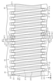
- FIG. 1 is a perspective view of the transformer chip of the first embodiment.
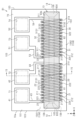
- 2 is a plan view of the transformer chip of FIG. 1.
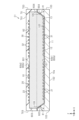
- FIG. 3 is a cross-sectional view taken along line 3-3 of FIG. 2.
- FIG. 4 is a cross-sectional view taken along line 4-4 of FIG. 2.
- FIG. 5 is a plan view showing the first coil.
- FIG. 6 is a plan view showing the second coil.
- FIG. 7 is a circuit diagram showing an application example of the transformer chip.
- FIG. 8 is a perspective view of the transformer chip of the second embodiment.
- 9 is a plan view of the transformer chip of FIG. 8.
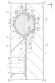
- FIG. 10 is a cross-sectional view taken along line 10-10 of FIG. 9.
- FIG. 11 is a cross-sectional view taken along line 11-11 of FIG. 9.
- FIG. FIG. 10 is a cross-sectional view taken along line 10-10 of FIG. 9.
- FIG. 11 is a cross-sectional view taken along line 11-11 of FIG. 9.
- FIG. 12 is a perspective view of the transformer chip of the third embodiment.
- 13 is a plan view of the transformer chip of FIG. 12.
- FIG. 14 is a cross-sectional view taken along line 14-14 of FIG. 13.
- FIG. 15 is a cross-sectional view taken along line 15-15 of FIG. 13.
- FIG. 16 is a cross-sectional view of a modified transformer chip.
- FIG. 17 is a cross-sectional view of a modified transformer chip.
- FIG. 18 is a plan view of a modified transformer chip.
- FIG. 19 is a plan view of a modified transformer chip.
- FIG. 20 is a plan view of a modified transformer chip.
- FIG. 21 is a plan view of a modified transformer chip.
- FIG. 22 is a plan view of a modified transformer chip.
- FIG. 23 is a plan view of a modified transformer chip.
- FIG. 24 is a cross-sectional view of a modified transformer chip.
- FIG. 1 is a perspective view of the transformer chip A1.
- FIG. 2 is a plan view of the transformer chip A1.
- 3 is a cross-sectional view taken along line 3-3 of FIG. 2.
- FIG. 4 is a cross-sectional view taken along line 4-4 of FIG. 2.
- FIG. 5 is an enlarged plan view showing the first coil 20.
- FIG. 6 is an enlarged plan view showing the second coil 30.
- FIG. 7 is a circuit diagram showing an application example of the transformer chip A1.
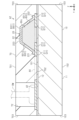
- the transformer chip A1 has a substrate 10, a first coil 20, a second coil 30, input pads 41 and 42, output pads 51 and 52, an insulating member 60 and a sealing resin 70. are doing.
- the substrate 10 is formed in a substantially flat plate shape.
- the thickness direction of the substrate 10 is defined as the Z direction.
- the first direction and the second direction that are orthogonal to each other are defined as the X direction and the Y direction, respectively.
- the substrate 10 is formed in a rectangular shape with long sides in the X direction and short sides in the Y direction when viewed from the Z direction.
- the substrate 10 has a substrate main surface 101 , a substrate back surface 102 and a plurality of substrate side surfaces 103 .
- the substrate main surface 101 and the substrate back surface 102 face opposite sides in the Z direction.
- the substrate main surface 101 and the substrate back surface 102 are flat surfaces.
- the plurality of substrate side surfaces 103 face either the X direction or the Y direction.
- the plurality of substrate side surfaces 103 are surfaces sandwiched between the substrate main surface 101 and the substrate back surface 102 .
- the substrate 10 of this embodiment is composed of a substrate body 11 and an insulating film 12 .
- the substrate body 11 is configured by, for example, a semiconductor substrate.
- the insulating film 12 is a film having electrical insulation. Note that the substrate 10 may be made of an insulating resin.
- the substrate main body 11 of this embodiment is a substrate formed from a material containing Si (silicon).
- a wide bandgap semiconductor or a compound semiconductor may be used as a semiconductor substrate for the substrate 10 .
- the wide bandgap semiconductor may be SiC (silicon carbide).
- the compound semiconductor may be a III-V compound semiconductor.
- the compound semiconductor may contain at least one of AlN (aluminum nitride), InN (indium nitride), GaN (gallium nitride), and GaAs (gallium arsenide).
- the substrate main body 11 may be an insulating substrate made of a material containing glass instead of the semiconductor substrate. Further, as the substrate main body 11, a substrate made of a synthetic resin whose main material is an epoxy resin or the like may be used.
- Insulating film 12 is made of, for example, SiO 2 (silicon oxide). This insulating film 12 is formed by thermally oxidizing the substrate body 11, which is, for example, a Si substrate.
- the material and formation method of the insulating film 12 are not limited.
- insulating film 12 may be made of a material containing SiO 2 and resin.
- the insulating film 12 may be made of SiN (silicon nitride), AiN (aluminum nitride), or the like.
- the insulating film 12 may be made of resin.
- the substrate 10 includes the substrate body 11 and the insulating film 12.
- the substrate 10 has a substrate main surface 101 , a substrate back surface 102 and a plurality of substrate side surfaces 103 .
- the substrate main surface 101 is composed of the surface of the insulating film 12 .
- the substrate back surface 102 is configured by the back surface of the substrate body 11 .
- the substrate side surface 103 is composed of the side surface of the substrate body 11 and the side surface of the insulating film 12 .
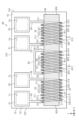
- the first coil 20 and the second coil 30 are arranged on the substrate main surface 101 of the substrate 10 .
- the first coil 20 and the second coil 30 are arranged along the substrate main surface 101 on the substrate main surface 101 .
- the first coil 20 and the second coil 30 are arranged side by side in the X direction on the main surface 101 of the substrate.
- the first coil 20 has a plurality of first substrate wirings 21 and a plurality of first connection wirings 22 .
- the first substrate wiring 21 and the first connection wiring 22 are made of a conductive metal such as Cu (copper), Cu alloy, or the like.
- the plurality of first substrate wirings 21 are provided on the substrate main surface 101 of the substrate 10 . As shown in FIG. 2, the plurality of first substrate wirings 21 are arranged along the X direction in which the first coils 20 and the second coils 30 are arranged. A plurality of first substrate wirings 21 are formed to extend along a direction crossing the X direction.
- each of the plurality of first substrate wirings 21 has a first end portion 211, a second end portion 212 opposite to the first end portion 211, and a first end portion 212. It has a first conductor portion 213 between the end portion 211 and the second end portion 212 .
- the first end portion 211 and the second end portion 212 are formed in a rectangular shape that is long in the Y direction with respect to the X direction when viewed from the Z direction.
- the first end portions 211 of the first substrate wirings 21 are arranged to be shifted in the X direction (rightward in FIG. 5) with respect to the second end portions 212 when viewed from the Z direction.
- the first end 211 of each first substrate wiring 21 is aligned with the second end 212 of the first substrate wiring 21 and each first substrate wiring 21 in the X direction. It is arranged between the second ends 212 of the adjacent first substrate wirings 21 .
- the first conductor portion 213 connects the first end portion 211 and the second end portion 212 . Therefore, the first conductor portion 213 of each first substrate wiring 21 extends at a predetermined angle with respect to the Y direction when viewed from the Z direction. As shown in FIG. 2 , the first conductor portion 213 is inclined toward the second coil 30 from the second end portion 212 toward the first end portion 211 when viewed in the Z direction. In other words, the first conductor portion 213 is inclined away from the second coil 30 from the first end portion 211 toward the second end portion 212 when viewed in the Z direction.
- the first coil 20 has a first connecting portion 23 at the end opposite to the second coil 30 .
- the first connection portion 23 is formed in a rectangular shape that is longer in the Y direction than in the X direction, like the first end portion 211 of the first substrate wiring 21 .
- the first connecting portion 23 is arranged at the same position as the first end portion 211 of each first substrate wiring 21 in the Y direction when viewed from the Z direction.
- the first connecting portion 23 is arranged at a position where the distance between the first end portions 211 adjacent in the X direction is equal to the distance between the first end portions 211 in the X direction when viewed from the Z direction.
- the insulating member 60 is formed so as to pass through the first coil 20 and the second coil 30. As shown in FIGS. That is, the insulating member 60 has a first end portion 603 that protrudes toward the side opposite to the second coil 30 in the first coil 20, and a portion that protrudes toward the side opposite to the first coil 20 in the second coil 30. and a second end 604 .
- Insulating member 60 is made of, for example, phenol resin, polyimide resin, or the like.
- the insulating member 60 has a first portion 61 corresponding to the first coil 20 and a second portion 62 corresponding to the second coil 30 .
- the first portion 61 is a portion arranged between the first substrate wiring 21 and the first connection wiring 22 of the first coil 20 .
- the second portion 62 is a portion arranged between the second substrate wiring 31 and the second connection wiring 32 of the second coil 30 .
- the insulating member 60 is formed so as to cover the first substrate wiring 21. As shown in FIG. Specifically, as shown in FIGS. 2, 4, and 5, the insulating member 60 is formed to expose the first end portion 211 and the second end portion 212 and cover the first conductor portion 213. As shown in FIGS. As shown in FIGS. 3 and 4 , the insulating member 60 is in contact with the main surface 101 of the substrate and is formed so as to cover the first conductor portion 213 of the first substrate wiring 21 . As shown in FIG. 3 , the insulating member 60 is in contact with the upper and side surfaces of the first conductor portion 213 .
- the insulating member 60 is formed so as to be in contact with the substrate main surface 101 in the Z direction and swell in the direction away from the substrate main surface 101 .
- the insulating member 60 has a cross-sectional shape in a plane (YZ plane) orthogonal to the X direction, which is arcuate and bulges in a direction away from the main surface 101 of the substrate.
- the insulating member 60 is formed in a strip shape extending in the X direction.
- the plurality of first connection wirings 22 are arranged along the X direction in which the first coils 20 and the second coils 30 are arranged.
- the plurality of first connection wirings 22 are formed to extend along a direction crossing the X direction.
- the first connection wiring 22 is in contact with the insulating member 60 and is formed so as to extend along the surface of the insulating member 60 having an arcuate cross-sectional shape in a plane perpendicular to the X direction.
- the first connection wiring 22 is formed so that the central portion thereof is separated from the first substrate wiring 21 by the insulating member 60 in the Z direction.
- Each of the plurality of first connection wirings 22 has a first end portion 211 of one first substrate wiring 21 and a second end portion 212 of the other first substrate wiring 21 of two first substrate wirings 21 adjacent to each other in the X direction. is formed to connect the
- each of the plurality of first connection wirings 22 has a third end portion 221, a fourth end portion 222 opposite to the third end portion 221, and a third end portion 222. It has a second conductor portion 223 between the end portion 221 and the fourth end portion 222 .
- the third end portion 221 and the fourth end portion 222 are formed in a rectangular shape that is long in the Y direction with respect to the X direction when viewed from the Z direction.
- the third end portions 221 of the first connection wirings 22 are arranged shifted in the X direction (rightward in FIG. 5) with respect to the fourth end portions 222 when viewed from the Z direction.
- the third end 221 of each first connection wiring 22 is aligned with the fourth end 222 of the first connection wiring 22 and each first connection wiring 22 in the X direction. It is arranged between the fourth ends 222 of the adjacent first connection wirings 22 .
- the third end 221 of the first connection wiring 22 is connected to the first end 211 of the first substrate wiring 21 .
- the fourth end 222 of the first connection wiring 22 is connected to the second end 212 of the first substrate wiring 21 adjacent to the first substrate wiring 21 to which the third end 221 is connected. That is, the plurality of first connection wirings 22 are connected between two first substrate wirings 21 adjacent in the X direction.
- the second conductor portion 223 connects the third end portion 221 and the fourth end portion 222 . Therefore, the second conductor portion 223 of each first connection wiring 22 extends at a predetermined angle with respect to the Y direction when viewed from the Z direction. As shown in FIG. 2 , the second conductor portion 223 is inclined away from the second coil 30 from the fourth end portion 222 toward the third end portion 221 when viewed in the Z direction. In other words, the second conductor portion 223 is inclined toward the second coil 30 from the third end portion 221 toward the fourth end portion 222 when viewed in the Z direction.
- the first connection wiring 22 is not connected to the first end portion 211 of the first substrate wiring 21X located at the end near the second coil 30 .
- the third end 221 of the first connection wiring 22X located at the end opposite to the second coil 30 is connected to the first connection portion 23 of the first coil 20. It is connected.
- the width of the first connection wiring 22 is formed narrower than the width of the first substrate wiring 21 .
- the first board wiring 21 has the first end portion 211 , the second end portion 212 and the first conductor portion 213 .
- the first end portion 211 and the second end portion 212 are formed in a rectangular shape that is long in the Y direction with respect to the X direction when viewed from the Z direction.
- the first connection wiring 22 has a third end portion 221 , a fourth end portion 222 and a second conductor portion 223 .
- the third end portion 221 and the fourth end portion 222 are formed in a rectangular shape that is long in the Y direction with respect to the X direction when viewed from the Z direction.
- the width W13 of the third end portion 221 is narrower than the width W11 of the first end portion 211.
- the length L13 of the third end portion 221 is shorter than the length L11 of the first end portion 211 .
- the width W14 of the fourth end 222 is narrower than the width W12 of the second end 212 .
- the length L14 of the fourth end 222 is shorter than the length L12 of the second end 212 .
- the width W11 of the first end 211 in the X direction is equal to the width W12 of the second end 212 in the X direction.
- the length L11 of the first end 211 in the Y direction is equal to the length L12 of the second end 212 in the Y direction.
- the width W13 of the third end portion 221 in the X direction is equal to the width W14 of the fourth end portion 222 in the X direction.
- the length L13 of the third end portion 221 in the Y direction is equal to the length L14 of the fourth end portion 222 in the Y direction.
- equal width and length include differences within the range of manufacturing error.
- the width of the first conductor portion 213 in the X direction is equal to the width of the first end portion 211 and the second end portion 212 .
- the width of the second conductor portion 223 in the X direction is equal to the width of the third end portion 221 and the fourth end portion 222 .
- the width of the first conductor portion 213 may be different from the widths of the first end portion 211 and the second end portion 212 .
- the width of the second conductor portion 223 may be different from the width of the third end portion 221 and the fourth end portion 222 .
- the second coil 30 has a plurality of second substrate wirings 31 and a plurality of second connection wirings 32.
- the second substrate wiring 31 and the second connection wiring 32 are made of a conductive metal such as Cu (copper), Cu alloy, or the like.
- the plurality of second substrate wirings 31 are provided on the substrate main surface 101 of the substrate 10 . As shown in FIG. 2, the plurality of second substrate wirings 31 are arranged along the X direction in which the first coils 20 and the second coils 30 are arranged. A plurality of second substrate wirings 31 are formed to extend along a direction crossing the X direction.
- each of the plurality of second substrate wirings 31 has a first end portion 311, a second end portion 312 opposite to the first end portion 311, and a first end portion 312. It has a first conductor portion 313 between the end portion 311 and the second end portion 312 .
- the first end portion 311 and the second end portion 312 are formed in a rectangular shape that is longer in the Y direction than in the X direction when viewed from the Z direction.
- the first ends 311 of the second substrate wirings 31 are arranged to be displaced in the X direction (to the right in FIG. 6) with respect to the second ends 312 when viewed from the Z direction.
- the first end 311 of each second substrate wiring 31 is aligned with the second end 312 of the second substrate wiring 31 and each second substrate wiring 31 in the X direction. It is arranged between the second ends 312 of the adjacent second substrate wirings 31 .
- the first conductor portion 313 connects the first end portion 311 and the second end portion 312 . Therefore, the first conductor portion 313 of each second substrate wiring 31 extends at a predetermined angle with respect to the Y direction when viewed from the Z direction. As shown in FIG. 2 , the first conductor portion 313 is inclined away from the first coil 20 from the second end portion 312 toward the first end portion 311 when viewed in the Z direction. In other words, the first conductor portion 313 is inclined toward the first coil 20 from the first end portion 311 toward the second end portion 312 when viewed in the Z direction.
- the second coil 30 has a second connecting portion 33 at the end on the first coil 20 side.
- the second connection portion 33 is formed in a rectangular shape that is longer in the Y direction than in the X direction.
- the second connection portion 33 is arranged at the same position as the first end portion 311 of each second substrate wiring 31 in the Y direction when viewed from the Z direction.
- the second connecting portion 33 is arranged at a position where the distance between the first end portions 311 adjacent to each other in the X direction is equal to the distance between the first end portions 311 in the X direction when viewed from the Z direction.
- the insulating member 60 is formed so as to cover the second board wiring 31. As shown in FIGS. Specifically, as shown in FIGS. 2 and 6, the insulating member 60 is formed to expose the first end portion 311 and the second end portion 312 and cover the first conductor portion 313 . As shown in FIG. 3 , the insulating member 60 is in contact with the substrate main surface 101 and is formed so as to cover the first conductor portion 313 of the second substrate wiring 31 . As shown in FIG. 3 , the insulating member 60 is in contact with the top and side surfaces of the first conductor portion 313 .
- the plurality of second connection wirings 32 are arranged along the X direction in which the first coils 20 and the second coils 30 are arranged.
- a plurality of second connection wirings 32 are formed to extend along a direction crossing the X direction.
- the second connection wiring 32 like the first connection wiring 22 of the first coil 20 shown in FIG. formed to extend along the The second connection wiring 32 is formed so that the central portion thereof is separated from the second substrate wiring 31 by the insulating member 60 in the Z direction.
- Each of the plurality of second connection wirings 32 has a first end portion 311 of one second substrate wiring 31 and a second end portion 312 of the other second substrate wiring 31 of two second substrate wirings 31 adjacent to each other in the X direction. is formed to connect the
- each of the plurality of second connection wirings 32 has a third end portion 321, a fourth end portion 322 opposite to the third end portion 321, and a third end portion 322. It has a second conductor portion 323 between the end portion 321 and the fourth end portion 322 .
- the third end portion 321 and the fourth end portion 322 are formed in a rectangular shape that is long in the Y direction with respect to the X direction when viewed from the Z direction.
- the third end portions 321 of the second connection wirings 32 are arranged to be shifted in the X direction (rightward in FIG. 6) with respect to the fourth end portions 322 when viewed from the Z direction.
- the third end 321 of each second connection wiring 32 is aligned with the fourth end 322 of the second connection wiring 32 and each second connection wiring 32 in the X direction. It is arranged between the fourth ends 322 of the adjacent second connection wirings 32 .
- the third end 321 of the second connection wiring 32 is connected to the first end 311 of the second substrate wiring 31 .
- the fourth end 322 of the second connection wiring 32 is connected to the second end 312 of the second substrate wiring 31 adjacent to the second substrate wiring 31 to which the third end 321 is connected. That is, the plurality of second connection wirings 32 are connected between two second substrate wirings 31 adjacent in the X direction.
- the second conductor portion 323 connects the third end portion 321 and the fourth end portion 322 . Therefore, the second conductor portion 323 of each second substrate wiring 31 extends at a predetermined angle with respect to the Y direction when viewed from the Z direction. As shown in FIG. 2 , the second conductor portion 323 is inclined toward the first coil 20 from the fourth end portion 322 toward the third end portion 321 when viewed in the Z direction. In other words, the second conductor portion 323 is inclined away from the first coil 20 from the third end portion 321 toward the fourth end portion 322 when viewed in the Z direction.
- the second connection wiring 32 is not connected to the first end portion 311 of the second substrate wiring 31X located at the end opposite to the first coil 20 in the second substrate wiring 31 of the present embodiment.
- the third end portion 321 of the second connection wiring 32X located at the end near the first coil 20 is connected to the second connection portion 33 of the second coil 30.
- the width of the second connection wiring 32 is formed narrower than the width of the second substrate wiring 31 .
- the second substrate wiring 31 has the first end portion 311 , the second end portion 312 and the first conductor portion 313 .
- the first end portion 311 and the second end portion 312 are formed in a rectangular shape that is longer in the Y direction than in the X direction when viewed from the Z direction.
- the second connection wiring 32 has a third end portion 321 , a fourth end portion 322 and a second conductor portion 323 .
- the third end portion 321 and the fourth end portion 322 are formed in a rectangular shape that is long in the Y direction with respect to the X direction when viewed from the Z direction.
- the width W23 of the third end portion 321 is narrower than the width W21 of the first end portion 311.
- the length L23 of the third end 321 is shorter than the length L21 of the first end 311 .
- width W24 of fourth end 322 is narrower than width W22 of second end 312 .
- the length L24 of the fourth end 322 is shorter than the length L22 of the second end 312 .
- the width W21 of the first end 311 in the X direction is equal to the width W22 of the second end 312 in the X direction.
- the length L21 of the first end portion 311 in the Y direction is equal to the length L22 of the second end portion 312 in the Y direction.
- the width W23 of the third end portion 321 in the X direction is equal to the width W24 of the fourth end portion 322 in the X direction.
- the length L23 of the third end portion 321 in the Y direction is equal to the length L24 of the fourth end portion 322 in the Y direction.
- the width of the first conductor portion 313 in the X direction is equal to the width of the first end portion 311 and the second end portion 312 .
- the width of the second conductor portion 323 in the X direction is equal to the width of the third end portion 321 and the fourth end portion 322 .
- the width of the first conductor portion 313 may be different from the widths of the first end portion 311 and the second end portion 312 .
- the width of the second conductor portion 323 may be different from the width of the third end portion 321 and the fourth end portion 322 .
- the first coil 20 and the second coil 30 are arranged with a predetermined distance D1.
- This distance D1 is the distance between the coils.
- the inter-coil distance may be defined by, for example, the distance between the first substrate wiring 21 and the second substrate wiring 31 and the distance between the first connection wiring 22 and the second connection wiring 32 .
- the inter-coil distance D ⁇ b>1 is set wider than the wiring interval P ⁇ b>1 of the first coils 20 .
- the wiring spacing P1 is defined as the spacing between two first substrate wirings 21 adjacent in the X direction.
- the inter-coil distance D1 is set wider than the wiring interval P2 of the second coils 30 .
- the wiring spacing P2 is defined as the spacing between two second substrate wirings 31 adjacent in the X direction.
- the wiring interval P1 of the first coil 20 and the wiring interval P2 of the second coil 30 are the same. Note that the wiring interval P1 between the first coils 20 and the wiring interval P2 between the second coils 30 may be different.
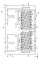
- the transformer chip A1 has input pads 41 and 42 and output pads 51 and 52 .
- the input pads 41 and 42 and the output pads 51 and 52 are formed in a rectangular shape when viewed from the Z direction.
- Input pads 41 and 42 and output pads 51 and 52 are configured to be connectable with bonding wires.
- the bonding wire BW connected to the input pad 42 is indicated by a chain double-dashed line. Bonding wires are connected to input pad 41 and output pads 51 and 52 shown in FIGS. 1 and 2 as well as input pad 42 .
- the input pads 41 and 42 are connected to the first coil 20. Specifically, the input pad 41 is connected to the first connection portion 23 of the first coil 20 by a pad connection wiring 43 .
- the input pad 42 is connected to the first end portion 211 of the first substrate wiring 21X of the first coil 20 by the pad connection wiring 44 .
- Input pads 41 and 42 and pad connection wirings 43 and 44 are made of a conductive metal such as Cu, Cu alloy, or the like.
- the output pads 51 and 52 are connected to the second coil 30. Specifically, the output pad 51 is connected to the second connection portion 33 of the second coil 30 by a pad connection wiring 53 .
- the output pad 52 is connected to the first end portion 311 of the second substrate wiring 31X of the second coil 30 by the pad connection wiring 54 .
- the output pads 51, 52 and the pad connection wirings 53, 54 are made of a conductive metal such as Cu, Cu alloy, or the like.
- the transformer chip A1 has a sealing resin 70.
- the sealing resin 70 is formed to have the same size as the substrate 10 when viewed from the Z direction.
- the sealing resin 70 has a resin main surface 701 , a resin back surface 702 and a plurality of resin side surfaces 703 .
- the resin main surface 701 and the resin back surface 702 face opposite sides in the Z direction.
- the resin main surface 701 faces the same direction as the substrate main surface 101 of the substrate 10 .
- the plurality of resin side surfaces 703 face either the X direction or the Y direction.
- the sealing resin 70 seals the first coil 20 and the second coil 30 .
- the sealing resin 70 has openings 71 and 72 that partially expose the input pads 41 and 42 .
- the sealing resin 70 has openings 73 and 74 that partially expose the output pads 51 and 52 .
- Sealing resin 70 is made of, for example, phenol resin, polyimide resin, or the like.
- the bonding wire BW is connected to the portion of the input pad 42 exposed from the opening 72 of the sealing resin 70 .
- bonding wires are connected to the portions of the sealing resin 70 exposed through the openings 71, 73 and 74 of the input pad 41 and the output pads 51 and 52 shown in FIGS.
- the transformer chip A1 of this embodiment can be used to insulate between inputs and outputs in various circuits.
- FIG. 7 shows an example of a circuit to which the transformer chip A1 of this embodiment is applied.
- This circuit applies a drive voltage signal to the gate of the switching element 91 .
- Switching element 91 configures inverter device 90 by being connected in series with switching element 92 .
- This inverter device 90 is mounted in, for example, an electric vehicle or a hybrid vehicle.
- the switching element 91 is, for example, a high-side switching element connected to a drive power supply.
- the switching element 92 is a low-side switching element.
- switching elements 91 and 92 include transistors such as SiMOSFETs (Si Metal-Oxide-Semiconductor Field-Effect Transistors), SiCMOSFETs, and IGBTs (Insulated Gate Bipolar Transistors). In the following description, it is assumed that the switching elements 91 and 92 are SiCMOSFETs.
- Transformer chip A 1 is connected between low voltage circuit 94 and high voltage circuit 95 .
- the low voltage circuit 94 is connected to a control circuit (ECU: Electronic Control Unit) 93 that controls the switching elements 91 and 92 .
- the low voltage circuit 94 is connected to the high voltage circuit 95 via the transformer chip A1.
- the low voltage circuit 94 is configured to operate with the first voltage V1.
- the high voltage circuit 95 is configured to operate with a second voltage V2 higher than the first voltage V1.
- the first voltage V1 and the second voltage V2 are DC voltages.
- the ground GND1 of the low-voltage circuit 94 and the ground GND2 of the high-voltage circuit 95 are provided independently.
- the potential of the ground GND1 of the low-voltage circuit 94 is set as a first reference potential, and the potential of the ground GND2 of the high-voltage circuit 95 is set as a second reference potential.
- the first voltage V1 is the voltage from the first reference potential
- the second voltage V2 is the voltage from the second reference potential.
- This circuit is configured such that a signal is transmitted from the low voltage circuit 94 to the high voltage circuit 95 through the transformer chip A1 based on a control signal from the ECU 93, and a drive voltage signal is output from the high voltage circuit 95.
- a signal transmitted from the low-voltage circuit 94 to the high-voltage circuit 95, that is, a signal output from the low-voltage circuit 94 is a signal for driving the switching element 91, for example.
- This signal is, for example, a pulse signal.
- the high voltage circuit 95 generates a signal for driving the switching element 91 based on the signal received from the low voltage circuit 94 through the transformer chip A1 and applies the signal to the switching element 91 .
- Switching element 91 is turned on and off in response to a signal applied by high voltage circuit 95 .
- the transformer chip A1 is insulated between the first coil 20 and the second coil 30. Therefore, the transformer chip A1 provides isolation between the low voltage circuit 94 and the high voltage circuit 95. FIG. That is, the transformer chip A1 cuts off the transmission of the DC voltage between the low voltage circuit 94 and the high voltage circuit 95. FIG. On the other hand, the transformer chip A1 is configured to be able to transmit signals such as pulse signals between the low voltage circuit 94 and the high voltage circuit 95 .
- the first coil 20 of the transformer chip A1 is connected to the ground GND1 of the low voltage circuit 94.
- the second coil 30 of the transformer chip A1 is connected to the ground GND2 of the high voltage circuit 95.
- a ground GND2 of the high voltage circuit 95 is connected to the source terminal of the switching element 91 driven by the high voltage circuit 95 . Therefore, the potential at one terminal of the second coil 30 becomes the second reference potential.
- This second reference potential varies as the inverter device 90 is driven.
- the first coil 20 is connected to the ground GND1 of the first reference potential. Therefore, between the first coil 20 and the second coil 30, a dielectric strength corresponding to the fluctuating second reference potential is required.
- the transformer chip A1 of this embodiment has a first coil 20 and a second coil 30 provided on the substrate main surface 101 of the substrate 10 .
- the first coil 20 and the second coil 30 are arranged side by side on the substrate main surface 101 of the substrate 10 along the first direction.
- the first coil 20 has a plurality of first substrate wirings 21 and a plurality of first connection wirings 22 arranged in the X direction.
- the plurality of first substrate wirings 21 extends along a direction crossing the X direction.
- a plurality of first connection wirings 22 are connected between two first substrate wirings 21 adjacent to each other in the X direction.
- the second coil 30 has a plurality of second substrate wirings 31 and a plurality of second connection wirings 32 arranged in the X direction.
- a plurality of second substrate wirings 31 extend along a direction crossing the X direction.
- a plurality of second connection wirings 32 are connected between two second substrate wirings 31 adjacent to each other in the X direction.
- the position of the first coil 20 is defined by the positions of the first substrate wiring 21 and the first connection wiring 22 formed on the substrate main surface 101 of the substrate 10 .
- the position of the second coil 30 is defined by the positions of the second substrate wiring 31 and the second connection wiring 32 formed on the substrate main surface 101 of the substrate 10 .
- the dielectric strength of the transformer chip A1 is determined by the distance between the first coil 20 and the second coil 30. FIG. In other words, the dielectric strength of the transformer chip A1 is determined by the arrangement positions of the first coil 20 and the second coil 30 . Therefore, a transformer chip A1 having desired characteristics can be easily obtained. That is, the degree of freedom in designing the transformer chip A1 can be improved.
- the withstand voltage of the transformer chip A1 can be adjusted. Therefore, in the manufacturing process, the characteristics of the transformer chip A1 can be easily changed without changing the steps such as adding a new step. Therefore, the degree of freedom in designing the transformer chip A1 can be improved.
- the first coil 20 and the second coil 30 are formed by plating. Specifically, a mask having openings corresponding to the first substrate wiring 21 of the first coil 20 and the second substrate wiring 31 of the second coil 30 is formed, and plating metal is deposited in the openings of the mask.
- the mask is formed, for example, by exposing and developing a resist layer having photosensitivity. Therefore, the positions of the first coil 20 and the second coil 30 can be changed only by changing the positions of the openings in the mask. Therefore, the degree of freedom in designing the transformer chip A1 can be improved.
- the first connection wirings 22 and the first substrate wirings 21 are alternately connected along the X direction.
- One first connection wiring 22 and one first substrate wiring 21 constitute one coil portion (one turn) in the first coil 20 . That is, one first connection wiring 22 and one first board wiring 21 constitute a unit element of one turn of the first coil 20 . Therefore, the number of first substrate wirings 21 and the number of first connection wirings 22 correspond to the number of turns of the first coil 20 . Therefore, the number of turns of the first coil 20 can be easily changed by changing the number of the first substrate wirings 21 and the first connection wirings 22 formed on the substrate 10 . Therefore, the degree of freedom in designing the first coil 20 can be improved.
- the first substrate wiring 21 extends in a direction crossing the X direction.
- the first substrate wiring 21 and the first connection wiring 22 form one coil portion (one turn) of the first coil 20 .
- the length of one turn is determined by the length of the first substrate wiring 21 and the length of the first connection wiring 22 .
- the first substrate wiring 21 is formed on the substrate main surface 101 . Therefore, the length of the first substrate wiring 21 can be easily changed. Therefore, the degree of freedom in designing the first coil 20 can be improved.
- the second connection wiring 32 and the second substrate wiring 31 are alternately connected along the X direction.
- One second connection wiring 32 and one second substrate wiring 31 constitute one coil portion (one turn) of the second coil 30 . That is, one second connection wiring 32 and one second board wiring 31 constitute a unit element of one turn of the second coil 30 . Therefore, the number of second substrate wirings 31 and the number of second connection wirings 32 correspond to the number of turns of the second coil 30 . Therefore, the number of turns of the second coil 30 can be easily changed by changing the number of the second substrate wirings 31 and the second connection wirings 32 formed on the substrate 10 . Therefore, the degree of freedom in designing the second coil 30 can be improved.
- the third end 221 of the first connection wiring 22 is connected to the first end 211 of the first substrate wiring 21, and the fourth end 222 of the first connection wiring 22 is connected to , and the second end portion 212 of the first substrate wiring 21 .
- the length of the first connection wiring 22 can be easily changed according to the length of the first substrate wiring 21 . Therefore, the degree of freedom in designing the first coil 20 can be improved.
- the first connection wiring 22 is formed along the surface 601 of the insulating member 60. As shown in FIG. Therefore, the length of the first connection wiring 22 is defined by the cross-sectional shape of the insulating member 60 and the height of the insulating member 60 . Therefore, the length of the first connection wiring 22 can be easily changed according to the shape of the insulating member 60 . Therefore, the degree of freedom in designing the first coil 20 can be improved.
- the second connection wiring 32 is formed along the surface 601 of the insulating member 60. As shown in FIG. Therefore, the length of the second connection wiring 32 is defined by the cross-sectional shape of the insulating member 60 and the height of the insulating member 60 . Therefore, the length of the second connection wiring 32 can be easily changed according to the shape of the insulating member 60 . Therefore, the degree of freedom in designing the second coil 30 can be improved.
- the length of one turn in the first coil 20 is determined by the lengths of the first substrate wiring 21 and the first connection wiring 22 . As shown in FIG. 4 , the length of one turn of the first coil 20 is determined by the cross-sectional shape of the insulating member 60 when viewed from the X direction. That is, by changing the size of the insulating member 60, the length of one turn of the first coil 20 can be easily changed. The length of one turn of the second coil 30 can also be easily changed in the same manner as the first coil 20 . That is, in the transformer chip A1, the degree of freedom in designing the length of one turn of the first coil 20 and the second coil 30 can be improved.
- the width W13 of the third end portion 221 is narrower than the width W11 of the first end portion 211. Therefore, even if the formation position of the third end portion 221 is displaced in the X direction due to a manufacturing error, the third end portion 221 can be formed on the first end portion 211 . Also, the length L13 of the third end portion 221 is shorter than the length L11 of the first end portion 211 . Therefore, even if the formation position of the third end portion 221 is displaced in the Y direction due to a manufacturing error, the third end portion 221 can be formed on the first end portion 211 .
- the width W14 of the fourth end portion 222 is narrower than the width W12 of the second end portion 212. Therefore, even if the formation position of the fourth end portion 222 is displaced in the X direction due to manufacturing errors, the fourth end portion 222 can be formed on the second end portion 212 .
- the length L14 of the fourth end 222 is shorter than the length L12 of the second end 212 . Therefore, even if the formation position of the fourth end portion 222 is displaced in the Y direction due to a manufacturing error, the fourth end portion 222 can be formed on the second end portion 212 .
- the width W23 of the third end portion 321 is narrower than the width W21 of the first end portion 311. Therefore, even if the formation position of the third end portion 321 is displaced in the X direction due to a manufacturing error, the third end portion 321 can be formed on the first end portion 311 . Also, the length L23 of the third end portion 321 is shorter than the length L21 of the first end portion 311 . Therefore, even if the formation position of the third end portion 321 is displaced in the Y direction due to a manufacturing error, the third end portion 321 can be formed on the first end portion 311 .
- the width W24 of the fourth end 322 is narrower than the width W22 of the second end 312 . Therefore, even if the formation position of the fourth end portion 322 is shifted in the X direction due to a manufacturing error, the fourth end portion 322 can be formed on the second end portion 312 .
- the length L24 of the fourth end 322 is shorter than the length L22 of the second end 312 . Therefore, even if the formation position of the fourth end portion 322 is displaced in the Y direction due to a manufacturing error, the fourth end portion 322 can be formed on the second end portion 312 .
- the length L13 of the third end portion 221 of the first connection wiring 22 is shorter than the length L11 of the first end portion 211 of the first substrate wiring 21 in the Y direction.
- the difference between the length L13 of the third end portion 221 and the length L11 of the first end portion 211 is greater than the difference between the width W13 of the third end portion 221 and the width W11 of the first end portion 211 . That is, the third end portion 221 connected to the first end portion 211 is set to have a positional deviation in the Y direction larger than the positional deviation in the X direction.
- the positions of the third end portion 221 and the fourth end portion 222 in the Y direction are affected by the size of the insulating member 60 and the formation position in the Y direction. Therefore, the influence on the formation of the insulating member 60 can be reduced, and the first connection wiring 22 can be reliably connected to the first substrate wiring 21 .
- the length L14 of the fourth end 222 of the first connection wiring 22 is shorter than the length L12 of the second end 212 of the first substrate wiring 21 in the Y direction.
- the difference between the length L14 of the fourth end portion 222 and the length L12 of the second end portion 212 is greater than the difference between the width W13 of the fourth end portion 222 and the width W11 of the second end portion 212 .
- the fourth end portion 222 connected to the second end portion 212 is set to have a larger positional deviation in the Y direction than the positional deviation in the X direction.
- the fourth end 222 and the position of the fourth end 222 are affected by the size of the insulating member 60 and the formation position in the Y direction. Therefore, the influence on the formation of the insulating member 60 can be reduced, and the first connection wiring 22 can be reliably connected to the first substrate wiring 21 .
- the length L23 of the third end portion 321 of the second connection wiring 32 is shorter than the length L21 of the first end portion 311 of the second substrate wiring 31 in the Y direction.
- the difference between the length L23 of the third end portion 321 and the length L21 of the first end portion 311 is greater than the difference between the width W13 of the third end portion 321 and the width W11 of the first end portion 311 . That is, the third end portion 321 connected to the first end portion 311 is set to have a positional deviation in the Y direction larger than the positional deviation in the X direction.
- the positions of the third end portion 321 and the fourth end portion 322 in the Y direction are affected by the size of the insulating member 60 and the formation position in the Y direction. Therefore, the influence on the formation of the insulating member 60 can be reduced, and the second connection wiring 32 can be reliably connected to the second board wiring 31 .
- the length L24 of the fourth end portion 322 of the second connection wiring 32 is shorter than the length L22 of the second end portion 312 of the second substrate wiring 31 in the Y direction.
- the difference between the length L24 of the fourth end portion 322 and the length L22 of the second end portion 312 is greater than the difference between the width W13 of the fourth end portion 322 and the width W11 of the second end portion 312 . That is, the fourth end portion 322 connected to the second end portion 312 is set to have a positional deviation in the Y direction larger than the positional deviation in the X direction.
- the fourth end portion 322 and the position of the fourth end portion 322 are affected by the size of the insulating member 60 and the formation position in the Y direction. Therefore, the influence on the formation of the insulating member 60 can be reduced, and the second connection wiring 32 can be reliably connected to the second board wiring 31 .
- the transformer chip A1 has a first coil 20 and a second coil 30 provided on the substrate main surface 101 of the substrate 10 .
- the first coil 20 and the second coil 30 are arranged side by side on the substrate main surface 101 of the substrate 10 along the first direction.
- the first coil 20 has a plurality of first substrate wirings 21 and a plurality of first connection wirings 22 arranged in the X direction.
- the plurality of first substrate wirings 21 extends along a direction crossing the X direction.
- a plurality of first connection wirings 22 are connected between two first substrate wirings 21 adjacent to each other in the X direction.
- the second coil 30 has a plurality of second substrate wirings 31 and a plurality of second connection wirings 32 arranged in the X direction.
- a plurality of second substrate wirings 31 extend along a direction crossing the X direction.
- a plurality of second connection wirings 32 are connected between two second substrate wirings 31 adjacent to each other in the X direction.
- the position of the first coil 20 is defined by the positions of the first substrate wiring 21 and the first connection wiring 22 formed on the substrate main surface 101 of the substrate 10 .
- the position of the second coil 30 is defined by the positions of the second substrate wiring 31 and the second connection wiring 32 formed on the substrate main surface 101 of the substrate 10 .
- the dielectric strength of the transformer chip A1 is determined by the distance between the first coil 20 and the second coil 30. FIG. In other words, the dielectric strength of the transformer chip A1 is determined by the arrangement positions of the first coil 20 and the second coil 30 . Therefore, a transformer chip A1 having desired characteristics can be easily obtained. That is, the degree of freedom in designing the transformer chip A1 can be improved.
- the first coil 20 and the second coil 30 are formed by plating. Specifically, a mask having openings corresponding to the first substrate wiring 21 of the first coil 20 and the second substrate wiring 31 of the second coil 30 is formed, and plating metal is deposited in the openings of the mask.
- the mask is formed, for example, by exposing and developing a resist layer having photosensitivity. Therefore, the positions of the first coil 20 and the second coil 30 can be changed only by changing the positions of the openings in the mask. Therefore, the degree of freedom in designing the transformer chip A1 can be improved.
- the first connection wiring 22 and the first substrate wiring 21 are alternately connected along the X direction.
- One first connection wiring 22 and one first substrate wiring 21 constitute one coil portion (one turn) in the first coil 20 . That is, one first connection wiring 22 and one first board wiring 21 constitute a unit element of one turn of the first coil 20 . Therefore, the number of first substrate wirings 21 and the number of first connection wirings 22 correspond to the number of turns of the first coil 20 . Therefore, the number of turns of the first coil 20 can be easily changed by changing the number of the first substrate wirings 21 and the first connection wirings 22 formed on the substrate 10 . Therefore, the degree of freedom in designing the first coil 20 can be improved.
- the first substrate wiring 21 extends in a direction crossing the X direction.
- the first substrate wiring 21 and the first connection wiring 22 form one coil portion (one turn) of the first coil 20 .
- the length of one turn is determined by the length of the first substrate wiring 21 and the length of the first connection wiring 22 .
- the first substrate wiring 21 is formed on the substrate main surface 101 . Therefore, the length of the first substrate wiring 21 can be easily changed. Therefore, the degree of freedom in designing the first coil 20 can be improved.
- the second connection wiring 32 and the second substrate wiring 31 are alternately connected along the X direction.
- One second connection wiring 32 and one second substrate wiring 31 constitute one coil portion (one turn) of the second coil 30 . That is, one second connection wiring 32 and one second board wiring 31 constitute a unit element of one turn of the second coil 30 . Therefore, the number of second substrate wirings 31 and the number of second connection wirings 32 correspond to the number of turns of the second coil 30 . Therefore, the number of turns of the second coil 30 can be easily changed by changing the number of the second substrate wirings 31 and the second connection wirings 32 formed on the substrate 10 . Therefore, the degree of freedom in designing the second coil 30 can be improved.
- the third end 221 of the first connection wiring 22 is connected to the first end 211 of the first substrate wiring 21, and the fourth end 222 of the first connection wiring 22 is connected to the first substrate wiring. 21 is connected to the second end 212 of .
- the length of the first connection wiring 22 can be easily changed according to the length of the first substrate wiring 21 . Therefore, the degree of freedom in designing the first coil 20 can be improved.
- the first connection wiring 22 is formed along the surface 601 of the insulating member 60 . Therefore, the length of the first connection wiring 22 is defined by the cross-sectional shape of the insulating member 60 and the height of the insulating member 60 . Therefore, the length of the first connection wiring 22 can be easily changed according to the shape of the insulating member 60 . Therefore, the degree of freedom in designing the first coil 20 can be improved.
- the second connection wiring 32 is formed along the surface 601 of the insulating member 60 . Therefore, the length of the second connection wiring 32 is defined by the cross-sectional shape of the insulating member 60 and the height of the insulating member 60 . Therefore, the length of the second connection wiring 32 can be easily changed according to the shape of the insulating member 60 . Therefore, the degree of freedom in designing the second coil 30 can be improved.
- the length of one turn in the first coil 20 is determined by the lengths of the first substrate wiring 21 and the first connection wiring 22 .
- the length of one turn of the first coil 20 as viewed in the X direction is determined by the cross-sectional shape of the insulating member 60 . That is, by changing the size of the insulating member 60, the length of one turn of the first coil 20 can be easily changed.
- the length of one turn of the second coil 30 can also be easily changed in the same manner as the first coil 20 . That is, in the transformer chip A1, the degree of freedom in designing the length of one turn of the first coil 20 and the second coil 30 can be improved.
- the width W13 of the third end portion 221 is narrower than the width W11 of the first end portion 211. Therefore, even if the formation position of the third end portion 221 is displaced in the X direction due to a manufacturing error, the third end portion 221 can be formed on the first end portion 211 . Also, the length L13 of the third end portion 221 is shorter than the length L11 of the first end portion 211 . Therefore, even if the formation position of the third end portion 221 is displaced in the Y direction due to a manufacturing error, the third end portion 221 can be formed on the first end portion 211 .
- the width W14 of the fourth end portion 222 is narrower than the width W12 of the second end portion 212. Therefore, even if the formation position of the fourth end portion 222 is displaced in the X direction due to manufacturing errors, the fourth end portion 222 can be formed on the second end portion 212 .
- the length L14 of the fourth end 222 is shorter than the length L12 of the second end 212 . Therefore, even if the formation position of the fourth end portion 222 is displaced in the Y direction due to a manufacturing error, the fourth end portion 222 can be formed on the second end portion 212 .
- the width W23 of the third end portion 321 is narrower than the width W21 of the first end portion 311. Therefore, even if the formation position of the third end portion 321 is displaced in the X direction due to a manufacturing error, the third end portion 321 can be formed on the first end portion 311 . Also, the length L23 of the third end portion 321 is shorter than the length L21 of the first end portion 311 . Therefore, even if the formation position of the third end portion 321 is displaced in the Y direction due to a manufacturing error, the third end portion 321 can be formed on the first end portion 311 .
- the width W24 of the fourth end portion 322 is narrower than the width W22 of the second end portion 312. Therefore, even if the formation position of the fourth end portion 322 is shifted in the X direction due to a manufacturing error, the fourth end portion 322 can be formed on the second end portion 312 .
- the length L24 of the fourth end 322 is shorter than the length L22 of the second end 312 . Therefore, even if the formation position of the fourth end portion 322 is displaced in the Y direction due to a manufacturing error, the fourth end portion 322 can be formed on the second end portion 312 .
- the length L13 of the third end 221 of the first connection wiring 22 is shorter than the length L11 of the first end 211 of the first substrate wiring 21 .
- the difference between the length L13 of the third end portion 221 and the length L11 of the first end portion 211 is greater than the difference between the width W13 of the third end portion 221 and the width W11 of the first end portion 211 . That is, the third end portion 221 connected to the first end portion 211 is set to have a positional deviation in the Y direction larger than the positional deviation in the X direction.
- the positions of the third end portion 221 and the fourth end portion 222 in the Y direction are affected by the size of the insulating member 60 and the formation position in the Y direction. Therefore, the influence on the formation of the insulating member 60 can be reduced, and the first connection wiring 22 can be reliably connected to the first substrate wiring 21 .
- the length L14 of the fourth end 222 of the first connection wiring 22 is shorter than the length L12 of the second end 212 of the first substrate wiring 21 .
- the difference between the length L14 of the fourth end portion 222 and the length L12 of the second end portion 212 is greater than the difference between the width W13 of the fourth end portion 222 and the width W11 of the second end portion 212 .
- the fourth end portion 222 connected to the second end portion 212 is set to have a larger positional deviation in the Y direction than the positional deviation in the X direction.
- the fourth end 222 and the position of the fourth end 222 are affected by the size of the insulating member 60 and the formation position in the Y direction. Therefore, the influence on the formation of the insulating member 60 can be reduced, and the first connection wiring 22 can be reliably connected to the first substrate wiring 21 .
- the length L23 of the third end 321 of the second connection wiring 32 is shorter than the length L21 of the first end 311 of the second substrate wiring 31 .
- the difference between the length L23 of the third end portion 321 and the length L21 of the first end portion 311 is greater than the difference between the width W13 of the third end portion 321 and the width W11 of the first end portion 311 . That is, the third end portion 321 connected to the first end portion 311 is set to have a positional deviation in the Y direction larger than the positional deviation in the X direction.
- the positions of the third end portion 321 and the fourth end portion 322 in the Y direction are affected by the size of the insulating member 60 and the formation position in the Y direction. Therefore, the influence on the formation of the insulating member 60 can be reduced, and the second connection wiring 32 can be reliably connected to the second board wiring 31 .
- the length L24 of the fourth end 322 of the second connection wiring 32 is shorter than the length L22 of the second end 312 of the second substrate wiring 31 .
- the difference between the length L24 of the fourth end portion 322 and the length L22 of the second end portion 312 is greater than the difference between the width W13 of the fourth end portion 322 and the width W11 of the second end portion 312 . That is, the fourth end portion 322 connected to the second end portion 312 is set to have a positional deviation in the Y direction larger than the positional deviation in the X direction.
- the fourth end portion 322 and the position of the fourth end portion 322 are affected by the size of the insulating member 60 and the formation position in the Y direction. Therefore, the influence on the formation of the insulating member 60 can be reduced, and the second connection wiring 32 can be reliably connected to the second board wiring 31 .
- FIG. 8 is a perspective view of the transformer chip B1.
- FIG. 9 is a plan view of the transformer chip B1.
- 10 is a cross-sectional view taken along line 10-10 of FIG. 9.
- FIG. 11 is a cross-sectional view taken along line 11-11 of FIG. 9.
- FIG. 8 is a perspective view of the transformer chip B1.
- FIG. 9 is a plan view of the transformer chip B1.
- 10 is a cross-sectional view taken along line 10-10 of FIG. 9.
- FIG. 11 is a cross-sectional view taken along line 11-11 of FIG. 9.
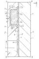
- the transformer chip B1 has a substrate 10a, a first coil 20, a second coil 30, input pads 41 and 42, output pads 51 and 52, an insulating member 60a and a sealing resin 70. are doing.
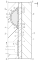
- the substrate 10a of this embodiment has recesses 13 on the main surface 101 of the substrate.
- the recess 13 is formed so as to be recessed toward the back surface 102 of the substrate.
- the concave portion 13 is formed in a rectangular shape when viewed from the Z direction.
- the substrate main surface 101 includes a frame-shaped upper surface 104 surrounding the recess 13 .
- the upper surface 104 includes a first upper surface 1041 and a second upper surface 1042 positioned so as to sandwich the recess 13 in the Y direction.
- Input pads 41 and 42 connected to the first coil 20 and output pads 51 and 52 connected to the second coil 30 are arranged on the first upper surface 1041 .
- the recess 13 is defined by a bottom surface 105 and a plurality of intermediate surfaces 106 between the bottom surface 105 and the top surface 104 .
- Substrate 10 a has a bottom surface 105 and an intermediate surface 106 that define recess 13 .
- Recess 13 and intermediate surface 106 are included in substrate major surface 101 . That is, the substrate main surface 101 of this embodiment includes a bottom surface 105 and an intermediate surface 106 that define the recess 13 and a top surface 104 around the recess 13 .
- Intermediate surface 106 includes a first intermediate surface 1061 between bottom surface 105 and first top surface 1041 and a second intermediate surface 1062 between bottom surface 105 and second top surface 1042 .
- the bottom surface 105 is formed in a rectangular shape elongated in the X direction.
- the intermediate surfaces 106 are located on both sides of the bottom surface 105 in the X direction.
- Intermediate surface 106 is inclined from bottom surface 105 toward upper surface 104 such that both intermediate surfaces 106, 106 are separated from each other.
- the intermediate surfaces 106 (1061, 1062) are located on both sides of the bottom surface 105 in the Y direction. Intermediate surfaces 1061 and 1062 are inclined from bottom surface 105 toward upper surface 104 so that both intermediate surfaces 1061 and 1062 are separated from each other.
- the substrate 10 a is composed of a substrate body 11 and an insulating film 12 .
- the substrate body 11 is composed of a semiconductor substrate.
- the insulating film 12 is a film having electrical insulation.
- the substrate body 11 is made of a semiconductor material that is a single crystal material.
- the substrate body 11 of this embodiment is a Si substrate.
- the insulating film 12 is made of SiO2 .
- the recess 13 is formed by etching (anisotropic etching) the substrate body 11 .
- the insulating film 12 is formed, for example, by thermally oxidizing the substrate body 11 having a recess.
- Insulating film 12 may be made of, for example, SiN (silicon nitride), AlN (aluminum nitride), or the like.
- the upper surface 104 of the substrate 10a has a plane orientation based on the crystal structure of Si, and is the (100) plane in this embodiment.
- the intermediate plane 106 is the ⁇ 111 ⁇ plane. Therefore, as shown in FIGS. 10 and 11, the inclination angle ⁇ 1 of the intermediate surface 106 with respect to the bottom surface 105 is based on the crystal structure of the Si substrate and is approximately 54.7°.
- the first coil 20 and the second coil 30 are arranged on the substrate main surface 101 of the substrate 10a.
- the first coil 20 and the second coil 30 are arranged along the substrate main surface 101 on the substrate main surface 101 .
- the first coil 20 and the second coil 30 are arranged side by side in the X direction on the main surface 101 of the substrate.
- the first coil 20 has a plurality of first substrate wirings 21 and a plurality of first connection wirings 22 .
- the first substrate wiring 21 and the first connection wiring 22 are made of a conductive metal such as Cu (copper), Cu alloy, or the like.
- the plurality of first substrate wirings 21 are provided on the substrate main surface 101 of the substrate 10a. As shown in FIG. 9, the plurality of first substrate wirings 21 are arranged along the X direction. A plurality of first substrate wirings 21 are formed to extend along a direction crossing the X direction.
- each of the plurality of first substrate wirings 21 has a first end portion 211, a second end portion 212 opposite to the first end portion 211, and a first end portion 211 and a first end portion 212. It has a first conductor portion 213 between the two ends 212 .
- the first coil 20 has a first connection portion 23 .
- the first substrate wiring 21 extends along the surface of the recess 13.
- the recess 13 is defined by a bottom surface 105 and intermediate surfaces 106 (1061, 1062) on both sides of the bottom surface 105.
- the substrate main surface 101 includes a first upper surface 1041 , a second upper surface 1042 and surfaces of the recesses 13 .
- the surface of recess 13 includes bottom surface 105 and intermediate surfaces 1061 and 1062 .
- the first substrate wiring 21 is in contact with the first upper surface 1041 , the intermediate surface 1061 , the bottom surface 105 , the intermediate surface 1062 and the second upper surface 1042 .
- a first end portion 211 of the first substrate wiring 21 is arranged on the first upper surface 1041 .
- a second end portion 212 of the first substrate wiring 21 is arranged on the second upper surface 1042 .
- the first conductor portion 213 between the first end portion 211 and the second end portion 212 is in contact with the intermediate surface 1061 , the bottom surface 105 and the intermediate surface 1062 .
- the first conductor portion 213 of this embodiment has a bottom portion 2133 in contact with the bottom surface 105 and side portions 2131 and 2132 in contact with the intermediate surfaces 1061 and 1062 .
- the insulating member 60a is formed so as to fill the recess 13. As shown in FIG. As shown in FIGS. 9 and 10, the insulating member 60a is formed so as to pass through the first coil 20 and the second coil 30. As shown in FIGS. In other words, the insulating member 60a has a first end portion 603 that protrudes from the first coil 20 toward the side opposite to the second coil 30, and a portion from the second coil 30 that protrudes toward the side opposite to the first coil 20. and a second end 604 .
- the insulating member 60 a has a first portion 61 corresponding to the first coil 20 and a second portion 62 corresponding to the second coil 30 .
- the first portion 61 is a portion arranged between the first substrate wiring 21 and the first connection wiring 22 of the first coil 20 .
- the second portion 62 is a portion arranged between the second substrate wiring 31 and the second connection wiring 32 of the second coil 30 .
- the insulating member 60a is formed so as to cover the first board wiring 21. As shown in FIGS. As shown in FIG. 11, the insulating member 60a is formed to expose the first end 211 and the second end 212 of the first board wiring 21 and cover the first conductor 213. As shown in FIG. The surface 601 of the insulating member 60a of the present embodiment is formed flat.
- the plurality of first connection wirings 22 are arranged along the X direction.
- the plurality of first connection wirings 22 are formed to extend along a direction crossing the X direction.
- the first connection wiring 22 is formed so as to be in contact with the insulating member 60a.
- the first connection wiring 22 is formed to extend along the surface 601 of the insulating member 60a.
- each of the plurality of first connection wirings 22 is connected to the first end portion 211 of one first substrate wiring 21 of two first substrate wirings 21 adjacent in the X direction and the other first substrate wiring 21 .
- the wiring 21 is connected to the second end 212 .
- each of the plurality of first connection wirings 22 has a third end 221, a fourth end 222 opposite to the third end 221, and a third end 222 opposite to the third end 221. It has a second conductor portion 223 between the third end portion 221 and the fourth end portion 222 .
- the third end 221 of the first connection wiring 22 is connected to the first end 211 of the first substrate wiring 21 .
- the fourth end 222 of the first connection wiring 22 is connected to the second end 212 of the first substrate wiring 21 .
- the second conductor portion 223 connects the third end portion 221 and the fourth end portion 222 .
- the first connection wiring 22 is not connected to the first end 211 of the first substrate wiring 21X located at the end near the second coil 30 in the first substrate wiring 21 .
- the third end 221 of the first connection wiring 22X located at the end opposite to the second coil 30 is connected to the first connection portion 23 of the first coil 20. It is connected.
- the second coil 30 has a plurality of second substrate wirings 31 and a plurality of second connection wirings 32 .
- the second substrate wiring 31 and the second connection wiring 32 are made of a conductive metal such as Cu (copper), Cu alloy, or the like.
- the plurality of second substrate wirings 31 are provided on the substrate main surface 101 of the substrate 10a. As shown in FIG. 9, the plurality of second substrate wirings 31 are arranged along the X direction. A plurality of second substrate wirings 31 are formed to extend along a direction crossing the X direction.
- the plurality of second substrate wirings 31 are provided on the substrate main surface 101 of the substrate 10a. As shown in FIG. 9, the plurality of second substrate wirings 31 are arranged along the X direction. A plurality of second substrate wirings 31 are formed to extend along a direction crossing the X direction.
- each of the plurality of second substrate wirings 31 has a first end portion 311, a second end portion 312 opposite to the first end portion 311, and a first end portion 311 and a second end portion 312, respectively. It has a first conductor portion 313 between the two ends 312 .
- the second coil 30 has a second connection portion 33 .
- the second substrate wiring 31 extends along the surface of the recess 13.
- the recess 13 is defined by a bottom surface 105 and intermediate surfaces 106 (1061, 1062) on both sides of the bottom surface 105.
- the substrate main surface 101 includes a first upper surface 1041 , a second upper surface 1042 and surfaces of the recesses 13 .
- the surface of recess 13 includes bottom surface 105 and intermediate surfaces 1061 and 1062 .
- the second substrate wiring 31 is in contact with the first upper surface 1041 , the intermediate surface 1061 , the bottom surface 105 , the intermediate surface 1062 and the second upper surface 1042 .
- a first end 311 of the second substrate wiring 31 is arranged on the first upper surface 1041 .
- a second end portion 312 of the second substrate wiring 31 is arranged on the second upper surface 1042 .
- the first conductor portion 313 between the first end portion 311 and the second end portion 312 contacts the intermediate surface 1061 , the bottom surface 105 and the intermediate surface 1062 .
- the first conductor portion 313 of the present embodiment has a bottom portion 3133 in contact with the bottom surface 105 and side portions 3131 and 3132 in contact with the intermediate surfaces 1061 and 1062 .
- the insulating member 60a is formed so as to cover the second board wiring 31. As shown in FIGS. As shown in FIG. 9, the insulating member 60a is formed to expose the first end 311 and the second end 312 of the second substrate wiring 31 and cover the first conductor 313. As shown in FIG.
- the plurality of second connection wirings 32 are arranged along the X direction.
- a plurality of second connection wirings 32 are formed to extend along a direction crossing the X direction.
- the second connection wiring 32 is formed so as to be in contact with the insulating member 60a.
- the second connection wiring 32 is formed to extend along the surface 601 of the insulating member 60a.
- each of the plurality of second connection wirings 32 is connected to the first end portion 311 of one of the two second substrate wirings 31 adjacent in the X direction and the other second substrate wiring 31 . It connects with the second end 312 of the wiring 31 .
- each of the plurality of second connection wirings 32 has a third end portion 321, a fourth end portion 322 opposite to the third end portion 321, and a third end portion 321 and a second conductor portion 323 between the fourth end portion 322 .
- the third end 321 of the second connection wiring 32 is connected to the first end 311 of the second substrate wiring 31 .
- a fourth end 322 of the second connection wiring 32 is connected to a second end 312 of the second substrate wiring 31 .
- the second conductor portion 323 connects the third end portion 321 and the fourth end portion 322 .
- the second connection wiring 32 is not connected to the first end portion 311 of the second substrate wiring 31X located at the end opposite to the first coil 20 in the second substrate wiring 31 of the present embodiment.
- the third end portion 321 of the second connection wiring 32X located at the end near the first coil 20 is connected to the second connection portion 33 of the second coil 30.
- the transformer chip B1 of this embodiment has a recess 13 in the substrate 10a.
- the insulating member 60 a is formed so as to fill the recess 13 . Therefore, the position of the insulating member 60a is determined by the position of the recess 13 of the substrate 10a. This increases the positional accuracy of the insulating member 60a compared to the case where the insulating member 60a is formed on a flat surface. Therefore, by forming the insulating member 60a so as to fill the recess 13, the influence of the insulating member 60a on the positions of the first connection wiring 22 of the first coil 20 and the second connection wiring 32 of the second coil 30 can be reduced. Thereby, in the first coil 20 and the second coil 30, the degree of freedom of design such as width and length can be improved.
- the first connection wiring 22 can be more reliably connected to the first substrate wiring 21.
- the second connection wiring 32 can be more reliably connected to the second substrate wiring 31 .
- the first connection wiring 22 of the first coil 20 is formed to extend along the surface 601 of the insulating member 60a embedded in the recess 13 of the substrate 10a.
- the second connection wiring 32 of the second coil 30 is formed to extend along the surface 601 of the insulating member 60a embedded in the recess 13 of the substrate 10a. Therefore, the thickness of the sealing resin 70 that seals the first coil 20 and the second coil 30 can be made thinner than in the first embodiment.
- the first substrate wiring 21 of the first coil 20 is formed so as to extend along the intermediate surface 1061 , the bottom surface 105 and the intermediate surface 1062 which are the inner surfaces of the recess 13 .
- the second substrate wiring 31 of the second coil 30 is formed to extend along the intermediate surface 1061 , the bottom surface 105 and the intermediate surface 1062 which are the inner surfaces of the recess 13 . Therefore, the lengths of the first substrate wiring 21 and the second substrate wiring 31 are set by the depth of the recess 13, which is the distance from the substrate main surface 101 of the substrate 10a to the bottom surface 105 of the recess 13 in the Z direction.
- the lengths of the first substrate wiring 21 and the second substrate wiring 31 and the lengths of the first connection wiring 22 and the second connection wiring 32 are set by the opening width of the recess 13 in the Y direction. Therefore, the depth of the recess 13 and the length of one turn of the first coil 20 and the second coil 30 can be adjusted.
- the transformer chip B1 of this embodiment has a recess 13 in the substrate 10a.
- the insulating member 60 a is formed so as to fill the recess 13 . Therefore, the position of the insulating member 60a is determined by the position of the recess 13 of the substrate 10a. This increases the positional accuracy of the insulating member 60a compared to the case where the insulating member 60a is formed on a flat surface. Therefore, by forming the insulating member 60a so as to fill the recess 13, the influence of the insulating member 60a on the positions of the first connection wiring 22 of the first coil 20 and the second connection wiring 32 of the second coil 30 can be reduced. Thereby, in the first coil 20 and the second coil 30, the degree of freedom of design such as width and length can be improved.
- the transformer chip B1 of the present embodiment can reduce the influence of the insulating member 60a on the positions of the first connection wiring 22 of the first coil 20 and the second connection wiring 32 of the second coil 30.
- FIG. Therefore, in the first coil 20 , the first connection wiring 22 can be more reliably connected to the first substrate wiring 21 .
- the second connection wiring 32 can be more reliably connected to the second substrate wiring 31 .
- the first connection wiring 22 of the first coil 20 is formed to extend along the surface 601 of the insulating member 60a embedded in the recess 13 of the substrate 10a.
- the second connection wiring 32 of the second coil 30 is formed to extend along the surface 601 of the insulating member 60a embedded in the recess 13 of the substrate 10a. Therefore, the thickness of the sealing resin 70 that seals the first coil 20 and the second coil 30 can be made thinner than in the first embodiment.
- the first board wiring 21 of the first coil 20 is formed so as to extend along the intermediate surface 1061 , the bottom surface 105 and the intermediate surface 1062 which are the inner surfaces of the recess 13 .
- the second substrate wiring 31 of the second coil 30 is formed to extend along the intermediate surface 1061 , the bottom surface 105 and the intermediate surface 1062 which are the inner surfaces of the recess 13 . Therefore, the lengths of the first substrate wiring 21 and the second substrate wiring 31 are set by the depth of the recess 13, which is the distance from the substrate main surface 101 of the substrate 10a to the bottom surface 105 of the recess 13 in the Z direction.
- the lengths of the first substrate wiring 21 and the second substrate wiring 31 and the lengths of the first connection wiring 22 and the second connection wiring 32 are set by the opening width of the recess 13 in the Y direction. Therefore, the depth of the recess 13 and the length of one turn of the first coil 20 and the second coil 30 can be adjusted.
- FIG. 12 A transformer chip C1 according to the third embodiment will be described with reference to FIGS. 12 to 15.
- FIG. 12 the same components as those of the transformer chip A1 of the first embodiment and the transformer chip B1 of the second embodiment are denoted by the same reference numerals, and part or all of the description thereof will be omitted. do.
- FIG. 12 is a perspective view of the transformer chip C1.
- FIG. 13 is a plan view of the transformer chip C1.
- 14 is a cross-sectional view taken along line 14-14 of FIG. 13.
- FIG. 15 is a cross-sectional view taken along line 15-15 of FIG. 13.
- the transformer chip C1 has a substrate 10a, a first coil 20, a second coil 30, input pads 41 and 42, output pads 51 and 52, an insulating member 60b, and a sealing resin 70. .
- the transformer chip C1 of this embodiment has the substrate 10a of the second embodiment.
- the substrate 10a has the recess 13 in this embodiment.
- the first coil 20 has a first substrate wiring 21 arranged on the substrate main surface 101 of the substrate 10a.
- the second coil 30 has a second substrate wiring 31 arranged on the substrate main surface 101 of the substrate 10a.
- the insulating member 60b is formed so as to cover the first board wiring 21 of the first coil 20 and the second board wiring 31 of the second coil 30.
- the insulating member 60b is made of, for example, phenol resin, polyimide resin, or the like.
- the insulating member 60b is formed to fill the recess 13 and protrude from the substrate main surface 101 toward the side opposite to the substrate back surface 102.
- the insulating member 60b of the present embodiment includes a first insulating portion 60b1 formed to fill the recess 13 and a second insulating portion 60b1 formed to protrude from the first insulating portion 60b1 toward the side opposite to the substrate back surface 102. and an insulating portion 60b2.
- the second insulating portion 60b2 has an arcuate cross-sectional shape that bulges away from the main surface 101 of the substrate on a plane (YZ plane) perpendicular to the X direction.
- the second substrate wiring 31 of the second coil 30 extends from the first upper surface 1041 toward the second upper surface 1042 toward the intermediate surface 1061 , the bottom surface 105 , and the intermediate surface 1062 that constitute the surface of the recess 13 . formed along.
- the second connection wiring 32 of the second coil 30 is in contact with the surface 601 of the insulating member 60b and extends along the surface of the insulating member 60b having an arcuate cross-sectional shape in a plane orthogonal to the X direction. is formed as The second connection wiring 32 is formed so that the central portion thereof is separated from the second substrate wiring 31 in the Z direction by the insulating member 60b.
- the size of the first coil 20 is larger than those in the first and second embodiments.
- the second coil 30 is also similar to the first coil 20 . Therefore, in the transformer chip C1 of the present embodiment, the diameters of the first coil 20 and the second coil 30 can be increased when viewed from the X direction.
- the lengths of the first substrate wiring 21 and the first connection wiring 22 constituting the first coil 20 are It becomes longer than the first embodiment and the second embodiment. Therefore, the coil length of the first coil 20 can be made longer. As with the first coil 20, the second coil 30 can also have a longer coil length.
- the same effects as (2-2) and (2-3) of the second embodiment can be obtained.
- (3-3) The size of the first coil 20 is larger than those in the first and second embodiments when viewed from the X direction.
- the second coil 30 is also similar to the first coil 20 . Therefore, in the transformer chip C1 of the present embodiment, the diameters of the first coil 20 and the second coil 30 can be increased when viewed from the X direction.
- the lengths of the first substrate wiring 21 and the first connection wiring 22 constituting the first coil 20 The height is longer than those of the first embodiment and the second embodiment. Therefore, the coil length of the first coil 20 can be made longer.
- the second coil 30 can also have a longer coil length.
- FIG. 16 shows a modified trans-chip A2.
- the cross-sectional shape of the insulating member 60c is formed in a square shape.
- the cross-sectional shape of the insulating member 60c is formed in a trapezoidal shape in which the length in the Y direction gradually decreases as the distance from the main surface 101 of the substrate increases. Therefore, the surface 601 of the insulating member 60c has an upper surface 6011 and side surfaces 6012 and 6013 inclined in the Z direction with respect to the Y direction.
- the first connection wiring 22 of the first coil 20 is formed along the side surface 6012 , the top surface 6011 and the side surface 6013 .
- the second connection wiring 32 of the second coil 30 is formed along the side surface 6012 , the top surface 6011 and the side surface 6013 like the first connection wiring 22 of the first coil 20 .
- the transformer chip A2 having the insulating member 60c having such a shape can obtain the same effects as the transformer chip A1 of the first embodiment.
- FIG. 17 shows a modified transformer chip A3.
- the cross-sectional shape of the insulating member 60d is formed in a square shape.
- the cross-sectional shape of this insulating member 60d is formed in a rectangular shape. Therefore, the surface 601 of the insulating member 60d has an upper surface 6011 and side surfaces 6012 and 6013 facing the Y direction.
- the first connection wiring 22 of the first coil 20 is formed along the side surface 6012 , the top surface 6011 and the side surface 6013 .
- the second connection wiring 32 of the second coil 30 is formed along the side surface 6012 , the top surface 6011 and the side surface 6013 like the first connection wiring 22 of the first coil 20 .
- the transformer chip A3 having the insulating member 60d having such a shape can obtain the same effects as the transformer chip A1 of the first embodiment.
- the cross-sectional shape of the insulating member 60 is not limited to the shapes of the insulating member 60 of the first embodiment and the insulating members 60c and 60d of the modification.
- the surface of the insulating member may have a cross-sectional shape having a linear portion and a curved portion (arc portion).
- the upper second insulating portion 60b2 protruding from the substrate main surface 101 has the same cross-sectional shape as the insulating member 60c shown in FIG. can be Also, the second insulating portion 60b2 may have the same cross-sectional shape as the insulating member 60d shown in FIG. Further, for example, in a cross section viewed from the X direction, the surface of the insulating member 60b may have a cross-sectional shape having a linear portion and a curved portion (arc portion).
- FIG. 18 shows a modified trans-chip A4.
- the number of turns of the second coil 30 is greater than the number of turns of the first coil 20 for this transformer chip A4. That is, the number of the second substrate wirings 31 and the second connection wirings 32 of the second coil 30 is greater than the number of the first substrate wirings 21 and the first connection wirings 22 of the first coil 20 .
- the amplitude of the output signal is changed with respect to the amplitude of the input signal applied to the input pads 41 and 42 according to the ratio of the number of turns of the first coil 20 and the number of turns of the second coil 30. can be obtained from the output pads 51,52.
- FIG. 19 shows a modified transformer chip A5.
- the number of turns of the first coil 20 is greater than the number of turns of the second coil 30 for this transformer chip A5. That is, the number of the first substrate wirings 21 and the first connection wirings 22 of the first coil 20 is greater than the number of the second substrate wirings 31 and the second connection wirings 32 of the second coil 30 .
- the amplitude of the output signal is changed with respect to the amplitude of the input signal applied to the input pads 41 and 42 according to the ratio of the number of turns of the first coil 20 and the number of turns of the second coil 30. can be obtained from the output pads 51,52.
- FIG. 20 shows a modified transformer chip A6.
- This transformer chip A6 has a third coil 80 in addition to the first coil 20 and the second coil 30 .
- the third coil 80 is arranged between the first coils 20 and the second coils 30 arranged in the X direction.
- the third coil 80 is insulated from the first coil 20 and the second coil 30 .
- the number of turns of the third coil 80 is the same as the number of turns of the first coil 20 and the number of turns of the second coil 30 .
- the third coil 80 has a plurality of third substrate wirings 81 and a plurality of third connection wirings 82 in the same manner as the first coil 20 and the second coil 30 .
- the insulating member 60 is formed so as to pass through the first coil 20 , the third coil 80 and the second coil 30 .
- the insulating member 60 has a third portion 63 corresponding to the third coil 80 .
- the plurality of third substrate wirings 81 are arranged along the X direction.
- a plurality of third substrate wirings 81 are provided on the substrate main surface 101 of the substrate 10 .
- the plurality of third substrate wirings 81 are formed so as to extend along the direction crossing the X direction.
- the direction in which the third substrate wiring 81 extends is the same as the direction in which the first substrate wiring 21 and the second substrate wiring 31 extend.
- the direction in which the third substrate wiring 81 extends may be different from the direction in which the first substrate wiring 21 and the second substrate wiring 31 extend.
- Each of the plurality of third substrate wirings 81 has a first end portion 811, a second end portion 812, and a first conductor portion 813.
- the insulating member 60 is formed to expose the first end portion 811 and the second end portion 812 of the third substrate wiring 81 and cover the first conductor portion 813 .
- the plurality of third connection wirings 82 are arranged along the X direction.
- a plurality of third connection wirings 82 are formed to extend along a direction crossing the X direction.
- a plurality of third connection wirings 82 are formed to extend along the surface of the insulating member 60 .
- Each of the plurality of third connection wirings 82 is formed such that the central portion thereof is separated from the third substrate wiring 81 by the insulating member 60 in the Z direction.
- Each of the plurality of third connection wirings 82 has a first end portion 811 of one of the two third substrate wirings 81 adjacent to each other in the X direction and a second end portion 812 of the other third substrate wiring 81 .
- the third connection wiring 82 includes a third end portion 821 connected to the first end portion 811 , a fourth end portion 822 connected to the second end portion 812 , a third end portion 821 and a fourth end portion 822 . It has a second conductor portion 823 between.
- the third connection wiring 82 is not connected to the first end 811 of the third substrate wiring 81X located at the end near the second coil 30 . Further, the third coil 80 of this modified example has a third connection portion 83 at the end near the first coil 20, and the third end portion 821 of the third connection wiring 82X is connected to the third connection portion 83. ing.
- the third coil 80 of this modified example has an end connection wiring 84 that connects the first end 811 of the third substrate wiring 81X and the third connection portion 83 .
- the end connection wiring 84 configures the third coil 80 in a loop shape.
- the dielectric strength of the transformer chip A6 is set by the distance between the first coil 20 and the third coil 80 and the distance between the third coil 80 and the second coil 30. Therefore, by adjusting the relative position between the first coil 20 and the third coil 80 and the relative position between the third coil 80 and the second coil 30, the dielectric strength voltage of the transformer chip A6 can be easily changed. Therefore, the degree of freedom in designing the transformer chip A6 can be improved.
- the positions of the first coil 20, the second coil 30, and the third coil 80 can be changed by masks (resist films) that form the coils 20, 80, and 30, respectively. Therefore, the trans chip A6 can be easily obtained without adding a new process to the manufacturing process of the trans chip A6 or changing the number of repetitions of existing processes.
- the number of turns of the third coil 80 may be larger than the number of turns of the first coil 20 and the number of turns of the second coil 30, as in the transformer chip A7 of the modified example shown in FIG. Also, the number of turns of the third coil 80 may be smaller than the number of turns of the first coil 20 and the number of turns of the second coil 30 .
- FIG. 22 shows a modified transformer chip A8.
- the first connection wiring 22 of the first coil 20 is formed so as to extend along the direction orthogonal to the X direction, that is, along the Y direction.
- the second connection wiring 32 of the second coil 30 is formed to extend in a direction perpendicular to the X direction, that is, along the Y direction.
- the first substrate wiring 21 of the first coil 20 may be formed so as to extend along the direction perpendicular to the X direction, that is, along the Y direction.
- the second substrate wiring 31 of the second coil 30 may be formed so as to extend along the direction orthogonal to the X direction, that is, along the Y direction.
- FIG. 23 shows a modified trans-chip A9.
- the input pads 41 and 42 are connected to the first coil 20 at the end opposite to the second coil 30 with respect to the first coil 20.
- the output pads 51 and 52 are connected to the second coil 30 at the ends of the second coil 30 opposite to the first coil 20 .
- the input pad 41 is connected to the fourth end 222 of the first connection wiring 22X of the first connection wirings 22 of the first coil 20 near the second coil 30 by the bypass wiring 45 that bypasses the first coil 20. ing.
- the input pad 42 is connected to the first connection portion 23 of the first coil 20 by a connection wiring 46 .
- the output pad 51 is connected to the second connection portion 33 of the second coil 30 by a detour wiring 55 that bypasses the second coil 30 .
- the output pad 52 is connected by a connection wiring 56 to a fourth end 322 of the second connection wiring 32X farthest from the first coil 20 among the second connection wirings 32 of the second coil 30 .
- the transformer chip A9 of this modified example in which the input pads 41 and 42 and the first coil 20 are connected in this manner and the output pads 51 and 52 and the second coil 30 are connected in this manner, the transformer chip of the first embodiment is also used.
- the same effect as A1 can be obtained.
- FIG. 24 shows a modified trans-chip A10.
- a substrate 10b of this transformer chip A10 has a substrate body 11, an insulating film 12, and a substrate insulating layer .
- a substrate insulating layer 14 is formed on the upper surface of the insulating film 12 .
- the first coil 20 and the second coil 30 are formed on the substrate main surface 101 which is the top surface of the substrate insulating layer 14 .
- the substrate insulating layer 14 can be made of an insulating resin such as phenol resin, or an insulating material such as SiO 2 or SiN.
- the substrate insulating layer 14 can also be composed of two or more insulating layers.
- This transformer chip A10 can also obtain the same effects as the transformer chip A1 of the first embodiment. Incidentally, by forming a concave portion in the substrate insulating layer 14, the same configuration as the transformer chip B1 of the second embodiment and the transformer chip C1 of the third embodiment can be obtained.
- the insulating member 60 may be provided for each coil.
- the insulating member 60 may have a first portion 61 corresponding to the first coil 20 and a second portion 62 corresponding to the second coil 30 as separate members.
- the insulating member 60 may be provided with a first portion 61, a second portion 62, and a third portion 63 as separate members.
- the second portion 62 may be provided separately from the first portion 61 and the third portion 63 in the transformer chips A6 and A7 shown in FIGS.
- the first portion 61 may be provided as a separate member for the third portion 63 and the second portion 62 .
- the first coil (20) is provided on the main surface (101) of the substrate, extends along a direction intersecting the first direction (X), and includes a plurality of first coils arranged in the first direction (X).
- the second coil (30) is provided on the main surface (101) of the substrate, extends along a direction intersecting the first direction (X), and includes a plurality of second coils arranged in the first direction (X).
- the first substrate wiring (21) and the second substrate wiring (31) are provided with first ends (211, 311) and second ends (211, 311) opposite to the first ends (211, 311). 212, 312) and a first conductor portion (213, 313) between the first end (211, 311) and the second end (212, 312);
- the first substrate wiring (21) and the second substrate are in contact with the substrate main surface (101) and expose the first end (211, 311) and the second end (212, 312).
- An insulating member (60, 60a, 60b) covering the wiring (31) is provided,
- the first connection wiring (22) and the second connection wiring (32) are formed along the surface (601) of the insulating member (60, 60a, 60b), 1.
- the substrate (10) has a substrate back surface facing away from the substrate main surface (101) and a recess (13) recessed from the substrate main surface (101) toward the substrate back surface,
- the recess (13) is formed to extend along the first direction (X),
- the first substrate wiring (21) and the second substrate wiring (31) extend along the surface of the recess (13), 2.
- the insulating member (60b) has a first portion (60b1) filling the recess (13) and a second portion (60b2) protruding from the main surface (101) of the substrate,
- the first connection wiring (22) and the second connection wiring (32) are formed along the surface (601) of the second portion (60b2), 5.
- a coil-to-coil distance (D1) between the first coil (20) and the second coil (30) is a distance between two of the first board wirings (21) adjacent to each other in the first direction (X). Any one of appendices 1 to 7, wherein the wiring spacing (P1) is wider than the wiring spacing (P1) or the wiring spacing (P2) between two of the second substrate wirings (31) adjacent to each other in the first direction (X). Trans tip as described.
- the third coil (80) is a plurality of third substrate wirings (81) provided on the substrate main surface (101), extending in a direction crossing the first direction (X), and arranged in the first direction (X); a plurality of third connection wirings (82) arranged in the first direction (X) and respectively connected between two of the third substrate wirings (81) adjacent in the first direction (X); a connection wiring (84) connecting the third substrate wiring (81) at one end and the third connection wiring (82) at the other end in the first direction (X); is configured in a loop with 16.
- (Appendix 21) 21 Any one of appendices 1 to 20, wherein the substrate (10) has a substrate body (11) made of a semiconductor material and an insulating layer (12) covering a main surface of the substrate body (11). transformer chip described in .
Landscapes
- Engineering & Computer Science (AREA)
- Power Engineering (AREA)
- Microelectronics & Electronic Packaging (AREA)
- Physics & Mathematics (AREA)
- Condensed Matter Physics & Semiconductors (AREA)
- General Physics & Mathematics (AREA)
- Computer Hardware Design (AREA)
- Manufacturing & Machinery (AREA)
- Coils Or Transformers For Communication (AREA)
Abstract
トランスチップは、基板の基板主面に設けられた第1コイルおよび第2コイルを有する。第1コイルと第2コイルは、第1方向に沿って基板の基板主面に並べて配置されている。第1コイルは、X方向に配列された複数の第1基板配線および複数の第1接続配線有している。複数の第1基板配線は、X方向と交差する方向に沿って延びている。複数の第1接続配線、X方向に隣り合う2つの第1基板配線の間にそれぞれ接続されている。第2コイル、X方向に配列された複数の第2基板配線および複数の第2接続配線を有している。複数の第2基板配線は、X方向と交差する方向に沿って延びている。複数の第2接続配線は、X方向に隣り合う2つの第2基板配線の間にそれぞれ接続されている。
Description
本開示は、トランスチップに関するものである。
従来、トランスチップ等の絶縁素子は、電源電圧の異なる複数の半導体チップ間で信号を伝達する手段として用いられている。たとえば、特許文献1には、上下方向に間隔を空けて互いに対向して配置された2つのコイルを備えたトランスチップが開示されている。
ところで、上記のように構成されたトランスチップでは、2つのコイルの構成や配置によってトランスチップの特性が決定される。たとえば、トランスチップの絶縁耐圧は、2つのコイルの距離によって決定される。絶縁耐圧を変更しようとすると、2つのコイルの間の絶縁膜の厚さ、層数などによって距離を変更するため、トランスチップの製造プロセスの変更を要することとなり、変更に手間がかかる。このため、トランスチップのデバイス設計について改善の余地がある。
本開示の一態様であるトランスチップは、基板主面を有する基板と、前記基板主面に設けられた第1コイルと、前記基板主面において前記第1コイルに対して第1方向に離れた位置に設けられた第2コイルと、を含み、前記第1コイルは、前記基板主面に設けられ、前記第1方向と交差する方向に沿って延び、前記第1方向に配列された複数の第1基板配線と、前記第1方向に配列され、前記第1方向において隣り合う2つの前記第1基板配線の間にそれぞれ接続された複数の第1接続配線と、を有し、前記第2コイルは、前記基板主面に設けられ、前記第1方向と交差する方向に沿って延び、前記第1方向に配列された複数の第2基板配線と、前記第1方向に配列され、前記第1方向において隣り合う2つの前記第2基板配線の間にそれぞれ接続された複数の第2接続配線と、を有する。
本開示の一態様によれば、デバイス設計の自由度が高いトランスチップを提供することができる。
以下、添付図面を参照して本開示のトランスチップのいくつかの実施形態を説明する。なお、説明を簡単かつ明確にするために、図面に示される構成要素は必ずしも一定の縮尺で描かれていない。また、理解を容易にするために、断面図では、ハッチング線が省略されている場合がある。添付の図面は、本開示の実施形態を例示するに過ぎず、本開示を制限するものとみなされるべきではない。
以下の詳細な記載は、本開示の例示的な実施形態を具体化する装置、システム、および方法を含む。この詳細な記載は本来説明のためのものに過ぎず、本開示の実施形態またはこのような実施形態の適用および使用を限定することを意図しない。
本開示における「第1」、「第2」、「第3」等の用語は、単にラベルを付して用いたものであり、必ずしもそれらの対象物に順列を付することを意図していない。
(第1実施形態)
図1から図5を参照して、第1実施形態のトランスチップA1について説明する。
(第1実施形態)
図1から図5を参照して、第1実施形態のトランスチップA1について説明する。
図1は、トランスチップA1の斜視図である。図2は、トランスチップA1の平面図である。図3は、図2の3-3線断面図である。図4は、図2の4-4線断面図である。図5は、第1コイル20を拡大して示す平面図である。図6は、第2コイル30を拡大して示す平面図である。図7は、トランスチップA1の適用例を示す回路図である。
図1から図4に示すように、トランスチップA1は、基板10、第1コイル20、第2コイル30、入力パッド41,42、出力パッド51,52、絶縁部材60、封止樹脂70を有している。
[基板]
基板10は、概略平板状に形成されている。以降の説明において、基板10の厚さ方向をZ方向とする。そして、Z方向と直交する方向のうちの互いに直交する第1方向および第2方向をそれぞれX方向およびY方向とする。
基板10は、概略平板状に形成されている。以降の説明において、基板10の厚さ方向をZ方向とする。そして、Z方向と直交する方向のうちの互いに直交する第1方向および第2方向をそれぞれX方向およびY方向とする。
図2に示すように、基板10は、Z方向から視て、X方向を長辺とし、Y方向を短辺とする長方形状に形成されている。
基板10は、基板主面101、基板裏面102、複数の基板側面103を有している。基板主面101と基板裏面102は、Z方向において互いに反対側を向く。基板主面101および基板裏面102は、平坦面である。複数の基板側面103は、X方向とY方向のいずれかを向く。複数の基板側面103は、基板主面101と基板裏面102との間に挟まれた面である。
基板10は、基板主面101、基板裏面102、複数の基板側面103を有している。基板主面101と基板裏面102は、Z方向において互いに反対側を向く。基板主面101および基板裏面102は、平坦面である。複数の基板側面103は、X方向とY方向のいずれかを向く。複数の基板側面103は、基板主面101と基板裏面102との間に挟まれた面である。
本実施形態の基板10は、基板本体11と、絶縁膜12とから構成されている。基板本体11は、たとえば半導体基板により構成されている。絶縁膜12は、電気絶縁性を有する被膜である。なお、基板10は、絶縁性を有する樹脂により構成されてもよい。
本実施形態の基板本体11は、Si(シリコン)を含む材料から形成された基板である。なお、基板10は、半導体基板として、ワイドバンドギャップ半導体や化合物半導体が用いられてもよい。ワイドバンドギャップ半導体は、SiC(炭化シリコン)であってもよい。化合物半導体は、III-V族化合物半導体であってもよい。化合物半導体は、AlN(窒化アルミニウム)、InN(窒化インジウム)、GaN(窒化ガリウム)、およびGaAs(ヒ化ガリウム)のうち少なくとも1つを含んでいてもよい。また、基板本体11は、半導体基板に代えて、ガラスを含む材料で形成された絶縁基板が用いられてもよい。また、基板本体11として、エポキシ樹脂等を主材とした合成樹脂から構成された基板が用いられてもよい。
絶縁膜12は、たとえばSiO2(酸化シリコン)により構成されている。この絶縁膜12は、たとえばSi基板である基板本体11を熱酸化することにより形成される。なお、絶縁膜12の材質、形成方法は限定されない。たとえば、絶縁膜12は、SiO2と樹脂とを含むものにより構成されてもよい。また、絶縁膜12は、SiN(窒化シリコン)、AiN(窒化アルミニウム)、等により構成されてもよい。また、絶縁膜12は、樹脂により構成されてもよい。
上述したように、基板10は、基板本体11と絶縁膜12とを含む。基板10は、基板主面101、基板裏面102、複数の基板側面103を有している。基板主面101は、絶縁膜12の表面により構成される。基板裏面102は、基板本体11の裏面により構成される。基板側面103は、基板本体11の側面と絶縁膜12の側面とにより構成される。
[第1コイル、第2コイル、絶縁部材]
第1コイル20および第2コイル30は、基板10の基板主面101に配置されている。第1コイル20および第2コイル30は、基板主面101において、基板主面101に沿って配置されている。本実施形態において、第1コイル20および第2コイル30は、基板主面101において、X方向に並んで配置されている。
第1コイル20および第2コイル30は、基板10の基板主面101に配置されている。第1コイル20および第2コイル30は、基板主面101において、基板主面101に沿って配置されている。本実施形態において、第1コイル20および第2コイル30は、基板主面101において、X方向に並んで配置されている。
第1コイル20は、複数の第1基板配線21と複数の第1接続配線22とを有する。第1基板配線21および第1接続配線22は、たとえばCu(銅)、Cu合金、などの導電性金属により構成されている。
図1、図2に示すように、複数の第1基板配線21は、基板10の基板主面101に設けられている。図2に示すように、複数の第1基板配線21は、第1コイル20と第2コイル30とが配列されたX方向に沿って配列されている。複数の第1基板配線21は、X方向と交差する方向に沿って延びるように形成されている。
図2、図5に示すように、本実施形態において、複数の第1基板配線21はそれぞれ、第1端部211と、第1端部211と反対側の第2端部212と、第1端部211と第2端部212との間の第1導体部213とを有している。
第1端部211および第2端部212は、Z方向から視て、X方向に対してY方向に長い長方形状に形成されている。
本実施形態において、第1基板配線21の第1端部211はそれぞれ、Z方向から視て、第2端部212に対してX方向(図5において右方向)にずれて配置されている。また、各第1基板配線21の第1端部211は、Z方向から視て、X方向において、当該第1基板配線21の第2端部212と、各第1基板配線21とX方向に隣り合う第1基板配線21の第2端部212との間に配置されている。
本実施形態において、第1基板配線21の第1端部211はそれぞれ、Z方向から視て、第2端部212に対してX方向(図5において右方向)にずれて配置されている。また、各第1基板配線21の第1端部211は、Z方向から視て、X方向において、当該第1基板配線21の第2端部212と、各第1基板配線21とX方向に隣り合う第1基板配線21の第2端部212との間に配置されている。
第1導体部213は、第1端部211と第2端部212とを接続する。したがって、各第1基板配線21の第1導体部213は、Z方向から視て、Y方向に対して所定の角度を有して延びている。図2に示すように、第1導体部213は、Z方向から視て、第2端部212から第1端部211に向けて、第2コイル30に近づくように傾いている。言い換えると、第1導体部213は、Z方向から視て、第1端部211から第2端部212に向けて、第2コイル30から離れるように傾いている。
本実施形態において、第1コイル20は、第2コイル30とは反対側の端部に第1接続部23を有している。第1接続部23は、第1基板配線21の第1端部211と同様に、X方向に対してY方向に長い長方形状に形成されている。第1接続部23は、Z方向から視て、Y方向において各第1基板配線21の第1端部211と同じ位置に配置されている。また、第1接続部23は、Z方向から視て、X方向に隣り合う第1端部211との距離が、各第1端部211のX方向の距離と等しい位置に配置されている。
図2、図3に示すように、絶縁部材60は、第1コイル20および第2コイル30を貫通するように形成されている。つまり、絶縁部材60は、第1コイル20において第2コイル30とは反対側に向けて突出する第1端部603と、第2コイル30において第1コイル20とは反対側に向けて突出する第2端部604とを有している。絶縁部材60は、たとえばフェノール樹脂、ポリイミド樹脂、などから構成されている。
絶縁部材60は、第1コイル20に対応する第1部分61と、第2コイル30に対応する第2部分62とを有している。図3に示すように、第1部分61は、第1コイル20の第1基板配線21と第1接続配線22との間に配置された部分である。第2部分62は、第2コイル30の第2基板配線31と第2接続配線32との間に配置された部分である。
図2から図5に示すように、絶縁部材60は、第1基板配線21を覆うように形成されている。詳しくは、図2、図4,図5に示すように、絶縁部材60は、第1端部211および第2端部212を露出し、第1導体部213を覆うように形成されている。図3、図4に示すように、絶縁部材60は、基板主面101と接し、第1基板配線21の第1導体部213を覆うように形成されている。図3に示すように、絶縁部材60は、第1導体部213の上面および側面と接している。
図4に示すように、絶縁部材60は、Z方向において、基板主面101と接し、基板主面101から離れる方向に膨らむように形成されている。絶縁部材60は、X方向と直交する平面(YZ平面)において、絶縁部材60の断面形状は、基板主面101から離れる方向に膨らむ円弧状に形成されている。絶縁部材60は、X方向の延びる帯状に形成されている。
図2、図3、図5に示すように、複数の第1接続配線22は、第1コイル20と第2コイル30とが配列されたX方向に沿って配列されている。複数の第1接続配線22は、X方向と交差する方向に沿って延びるように形成されている。
図4に示すように、第1接続配線22は、絶縁部材60と接し、X方向と直交する平面における断面形状が円弧状の絶縁部材60の表面に沿って延びるように形成されている。第1接続配線22は、中央部分が絶縁部材60により、第1基板配線21に対してZ方向に離れるように形成されている。複数の第1接続配線22はそれぞれ、X方向に隣り合う2つの第1基板配線21の一方の第1基板配線21の第1端部211と他方の第1基板配線21の第2端部212とを接続するように形成されている。
図2、図5に示すように、本実施形態において、複数の第1接続配線22はそれぞれ、第3端部221と、第3端部221と反対側の第4端部222と、第3端部221と第4端部222との間の第2導体部223とを有している。
第3端部221および第4端部222は、Z方向から視て、X方向に対してY方向に長い長方形状に形成されている。
本実施形態において、第1接続配線22の第3端部221はそれぞれ、Z方向から視て、第4端部222に対してX方向(図5において右方向)にずれて配置されている。また、各第1接続配線22の第3端部221は、Z方向から視て、X方向において、当該第1接続配線22の第4端部222と、各第1接続配線22とX方向に隣り合う第1接続配線22の第4端部222との間に配置されている。
本実施形態において、第1接続配線22の第3端部221はそれぞれ、Z方向から視て、第4端部222に対してX方向(図5において右方向)にずれて配置されている。また、各第1接続配線22の第3端部221は、Z方向から視て、X方向において、当該第1接続配線22の第4端部222と、各第1接続配線22とX方向に隣り合う第1接続配線22の第4端部222との間に配置されている。
第1接続配線22の第3端部221は、第1基板配線21の第1端部211と接続されている。第1接続配線22の第4端部222は、第3端部221が接続された第1基板配線21と隣り合う第1基板配線21の第2端部212と接続されている。つまり、複数の第1接続配線22は、X方向に隣り合う2つの第1基板配線21の間にそれぞれ接続されている。
第2導体部223は、第3端部221と第4端部222とを接続する。したがって、各第1接続配線22の第2導体部223は、Z方向から視て、Y方向に対して所定の角度を有して延びている。図2に示すように、第2導体部223は、Z方向から視て、第4端部222から第3端部221に向けて、第2コイル30から離れるように傾いている。言い換えると、第2導体部223は、Z方向から視て、第3端部221から第4端部222に向けて、第2コイル30に近づくように傾いている。
本実施形態の第1基板配線21において、第2コイル30に近い端に位置する第1基板配線21Xの第1端部211には、第1接続配線22が接続されていない。そして、本実施形態の第1接続配線22において、第2コイル30とは反対側の端に位置する第1接続配線22Xの第3端部221は、第1コイル20の第1接続部23に接続されている。
図5に示すように、第1接続配線22の幅は、第1基板配線21の幅よりも狭く形成されている。
上述したように、第1基板配線21は、第1端部211、第2端部212、第1導体部213を有している。第1端部211および第2端部212は、Z方向から視て、X方向に対してY方向に長い長方形状に形成されている。
上述したように、第1基板配線21は、第1端部211、第2端部212、第1導体部213を有している。第1端部211および第2端部212は、Z方向から視て、X方向に対してY方向に長い長方形状に形成されている。
第1接続配線22は、第3端部221、第4端部222、第2導体部223を有している。第3端部221および第4端部222は、Z方向から視て、X方向に対してY方向に長い長方形状に形成されている。
第3端部221の幅W13は、第1端部211の幅W11よりも狭い。第3端部221の長さL13は、第1端部211の長さL11よりも短い。同様に、第4端部222の幅W14は、第2端部212の幅W12よりも狭い。第4端部222の長さL14は、第2端部212の長さL12よりも短い。
本実施形態において、X方向における第1端部211の幅W11は、X方向における第2端部212の幅W12と等しい。Y方向における第1端部211の長さL11は、Y方向における第2端部212の長さL12と等しい。また、X方向における第3端部221の幅W13は、X方向における第4端部222の幅W14と等しい。Y方向における第3端部221の長さL13は、Y方向における第4端部222の長さL14と等しい。なお、本明細書において、幅や長さが等しいとは、差異が製造上の誤差の範囲内にあることを含む。
本実施形態において、X方向における第1導体部213の幅は、第1端部211、第2端部212の幅と等しい。また、X方向における第2導体部223の幅は、第3端部221、第4端部222の幅と等しい。なお、第1導体部213の幅は、第1端部211、第2端部212の幅と相違していてもよい。また、第2導体部223の幅は、第3端部221、第4端部222の幅と相違していてもよい。
図2、図3に示すように、第2コイル30は、複数の第2基板配線31と複数の第2接続配線32とを有する。第2基板配線31および第2接続配線32は、たとえばCu(銅)、Cu合金、などの導電性金属により構成されている。
図1、図2に示すように、複数の第2基板配線31は、基板10の基板主面101に設けられている。図2に示すように、複数の第2基板配線31は、第1コイル20と第2コイル30とが配列されたX方向に沿って配列されている。複数の第2基板配線31は、X方向と交差する方向に沿って延びるように形成されている。
図2、図6に示すように、本実施形態において、複数の第2基板配線31はそれぞれ、第1端部311と、第1端部311と反対側の第2端部312と、第1端部311と第2端部312との間の第1導体部313とを有している。
第1端部311および第2端部312は、Z方向から視て、X方向に対してY方向に長い長方形状に形成されている。
本実施形態において、第2基板配線31の第1端部311はそれぞれ、Z方向から視て、第2端部312に対してX方向(図6において右方向)にずれて配置されている。また、各第2基板配線31の第1端部311は、Z方向から視て、X方向において、当該第2基板配線31の第2端部312と、各第2基板配線31とX方向に隣り合う第2基板配線31の第2端部312との間に配置されている。
本実施形態において、第2基板配線31の第1端部311はそれぞれ、Z方向から視て、第2端部312に対してX方向(図6において右方向)にずれて配置されている。また、各第2基板配線31の第1端部311は、Z方向から視て、X方向において、当該第2基板配線31の第2端部312と、各第2基板配線31とX方向に隣り合う第2基板配線31の第2端部312との間に配置されている。
第1導体部313は、第1端部311と第2端部312とを接続する。したがって、各第2基板配線31の第1導体部313は、Z方向から視て、Y方向に対して所定の角度を有して延びている。図2に示すように、第1導体部313は、Z方向から視て、第2端部312から第1端部311に向けて、第1コイル20から離れるように傾いている。言い換えると、第1導体部313は、Z方向から視て、第1端部311から第2端部312に向けて、第1コイル20に近づくように傾いている。
本実施形態において、第2コイル30は、第1コイル20の側の端部に第2接続部33を有している。第2接続部33は、第2基板配線31の第1端部311と同様に、X方向に対してY方向に長い長方形状に形成されている。第2接続部33は、Z方向から視て、Y方向において各第2基板配線31の第1端部311と同じ位置に配置されている。また、第2接続部33は、Z方向から視て、X方向に隣り合う第1端部311との距離が、各第1端部311のX方向の距離と等しい位置に配置されている。
図2、図3、図6に示すように、絶縁部材60は、第2基板配線31を覆うように形成されている。詳しくは、図2、図6に示すように、絶縁部材60は、第1端部311および第2端部312を露出し、第1導体部313を覆うように形成されている。図3に示すように、絶縁部材60は、基板主面101と接し、第2基板配線31の第1導体部313を覆うように形成されている。図3に示すように、絶縁部材60は、第1導体部313の上面および側面と接している。
図2、図3、図6に示すように、複数の第2接続配線32は、第1コイル20と第2コイル30とが配列されたX方向に沿って配列されている。複数の第2接続配線32は、X方向と交差する方向に沿って延びるように形成されている。
第2接続配線32は、図4に示す第1コイル20の第1接続配線22と同様に、絶縁部材60と接し、X方向と直交する平面における断面形状が円弧状の絶縁部材60の表面に沿って延びるように形成されている。第2接続配線32は、中央部分が絶縁部材60により、第2基板配線31に対してZ方向に離れるように形成されている。複数の第2接続配線32はそれぞれ、X方向に隣り合う2つの第2基板配線31の一方の第2基板配線31の第1端部311と他方の第2基板配線31の第2端部312とを接続するように形成されている。
図2、図6に示すように、本実施形態において、複数の第2接続配線32はそれぞれ、第3端部321と、第3端部321と反対側の第4端部322と、第3端部321と第4端部322との間の第2導体部323とを有している。
第3端部321および第4端部322は、Z方向から視て、X方向に対してY方向に長い長方形状に形成されている。
本実施形態において、第2接続配線32の第3端部321はそれぞれ、Z方向から視て、第4端部322に対してX方向(図6において右方向)にずれて配置されている。また、各第2接続配線32の第3端部321は、Z方向から視て、X方向において、当該第2接続配線32の第4端部322と、各第2接続配線32とX方向に隣り合う第2接続配線32の第4端部322との間に配置されている。
本実施形態において、第2接続配線32の第3端部321はそれぞれ、Z方向から視て、第4端部322に対してX方向(図6において右方向)にずれて配置されている。また、各第2接続配線32の第3端部321は、Z方向から視て、X方向において、当該第2接続配線32の第4端部322と、各第2接続配線32とX方向に隣り合う第2接続配線32の第4端部322との間に配置されている。
第2接続配線32の第3端部321は、第2基板配線31の第1端部311と接続されている。第2接続配線32の第4端部322は、第3端部321が接続された第2基板配線31と隣り合う第2基板配線31の第2端部312と接続されている。つまり、複数の第2接続配線32は、X方向に隣り合う2つの第2基板配線31の間にそれぞれ接続されている。
第2導体部323は、第3端部321と第4端部322とを接続する。したがって、各第2基板配線31の第2導体部323は、Z方向から視て、Y方向に対して所定の角度を有して延びている。図2に示すように、第2導体部323は、Z方向から視て、第4端部322から第3端部321に向けて、第1コイル20に近づくように傾いている。言い換えると、第2導体部323は、Z方向から視て、第3端部321から第4端部322に向けて、第1コイル20から離れるように傾いている。
本実施形態の第2基板配線31において、第1コイル20とは反対側の端に位置する第2基板配線31Xの第1端部311には、第2接続配線32が接続されていない。そして、本実施形態の第2接続配線32において、第1コイル20に近い端に位置する第2接続配線32Xの第3端部321は、第2コイル30の第2接続部33に接続されている。
図6に示すように、第2接続配線32の幅は、第2基板配線31の幅よりも狭く形成されている。
上述したように、第2基板配線31は、第1端部311、第2端部312、第1導体部313を有している。第1端部311および第2端部312は、Z方向から視て、X方向に対してY方向に長い長方形状に形成されている。
上述したように、第2基板配線31は、第1端部311、第2端部312、第1導体部313を有している。第1端部311および第2端部312は、Z方向から視て、X方向に対してY方向に長い長方形状に形成されている。
第2接続配線32は、第3端部321、第4端部322、第2導体部323を有している。第3端部321および第4端部322は、Z方向から視て、X方向に対してY方向に長い長方形状に形成されている。
第3端部321の幅W23は、第1端部311の幅W21よりも狭い。第3端部321の長さL23は、第1端部311の長さL21よりも短い。同様に、第4端部322の幅W24は、第2端部312の幅W22よりも狭い。第4端部322の長さL24は、第2端部312の長さL22よりも短い。
本実施形態において、X方向における第1端部311の幅W21は、X方向における第2端部312の幅W22と等しい。Y方向における第1端部311の長さL21は、Y方向における第2端部312の長さL22と等しい。また、X方向における第3端部321の幅W23は、X方向における第4端部322の幅W24と等しい。Y方向における第3端部321の長さL23は、Y方向における第4端部322の長さL24と等しい。
本実施形態において、X方向における第1導体部313の幅は、第1端部311、第2端部312の幅と等しい。また、X方向における第2導体部323の幅は、第3端部321、第4端部322の幅と等しい。なお、第1導体部313の幅は、第1端部311、第2端部312の幅と相違していてもよい。また、第2導体部323の幅は、第3端部321、第4端部322の幅と相違していてもよい。
図2に示すように、第1コイル20と第2コイル30とは、所定の距離D1はなれて配置されている。この距離D1は、コイル間距離である。なお、コイル間距離は、たとえば第1基板配線21と第2基板配線31との間の距離、第1接続配線22と第2接続配線32との間の距離により規定されてもよい。コイル間距離D1は、第1コイル20の配線間隔P1よりも広く設定されている。配線間隔P1は、X方向に隣り合う2つの第1基板配線21の間の間隔として規定される。また、コイル間距離D1は、第2コイル30の配線間隔P2よりも広く設定されている。配線間隔P2は、X方向に隣り合う2つの第2基板配線31の間の間隔として規定される。本実施形態において、第1コイル20の配線間隔P1と第2コイル30の配線間隔P2は同一である。なお、第1コイル20の配線間隔P1と第2コイル30の配線間隔P2とが相違していてもよい。
[入力パッド、出力パッド]
図1、図2に示すように、トランスチップA1は、入力パッド41,42、出力パッド51,52を備えている。入力パッド41,42および出力パッド51,52は、Z方向から視て矩形状に形成されている。入力パッド41,42および出力パッド51,52は、ボンディングワイヤを接続可能に構成されている。図4では、入力パッド42に接続されるボンディングワイヤBWを二点鎖線にて示している。図1、図2に示す入力パッド41および出力パッド51,52についても入力パッド42と同様にボンディングワイヤが接続される。
図1、図2に示すように、トランスチップA1は、入力パッド41,42、出力パッド51,52を備えている。入力パッド41,42および出力パッド51,52は、Z方向から視て矩形状に形成されている。入力パッド41,42および出力パッド51,52は、ボンディングワイヤを接続可能に構成されている。図4では、入力パッド42に接続されるボンディングワイヤBWを二点鎖線にて示している。図1、図2に示す入力パッド41および出力パッド51,52についても入力パッド42と同様にボンディングワイヤが接続される。
入力パッド41,42は、第1コイル20に接続されている。詳しくは、入力パッド41は、パッド接続配線43により、第1コイル20の第1接続部23に接続されている。入力パッド42は、パッド接続配線44により、第1コイル20の第1基板配線21Xの第1端部211に接続されている。入力パッド41,42およびパッド接続配線43,44は、たとえばCu、Cu合金、などの導電性金属により構成されている。
出力パッド51,52は、第2コイル30に接続されている。詳しくは、出力パッド51は、パッド接続配線53により、第2コイル30の第2接続部33に接続されている。出力パッド52は、パッド接続配線54により、第2コイル30の第2基板配線31Xの第1端部311に接続されている。出力パッド51,52およびパッド接続配線53,54は、たとえばCu、Cu合金、などの導電性金属により構成されている。
[封止樹脂]
図1から図4に示すように、トランスチップA1は、封止樹脂70を備えている。封止樹脂70は、Z方向から見て、基板10と同じ大きさに形成されている。封止樹脂70は、樹脂主面701、樹脂裏面702、複数の樹脂側面703を有している。樹脂主面701および樹脂裏面702は、Z方向において互いに反対側を向く。樹脂主面701は、基板10の基板主面101と同じ方向を向く。複数の樹脂側面703は、X方向とY方向のいずれかを向く。
図1から図4に示すように、トランスチップA1は、封止樹脂70を備えている。封止樹脂70は、Z方向から見て、基板10と同じ大きさに形成されている。封止樹脂70は、樹脂主面701、樹脂裏面702、複数の樹脂側面703を有している。樹脂主面701および樹脂裏面702は、Z方向において互いに反対側を向く。樹脂主面701は、基板10の基板主面101と同じ方向を向く。複数の樹脂側面703は、X方向とY方向のいずれかを向く。
封止樹脂70は、第1コイル20および第2コイル30を封止する。封止樹脂70は、入力パッド41,42の一部を露出する開口71,72を有している。また、封止樹脂70は、出力パッド51,52の一部を露出する開口73,74を有している。封止樹脂70は、たとえばフェノール樹脂、ポリイミド樹脂、などから構成されている。図4に示すように、ボンディングワイヤBWは、封止樹脂70の開口72から露出する入力パッド42の部分に接続される。図示しないが、図1、図2に示す入力パッド41、出力パッド51,52に対して、封止樹脂70の開口71,73,74により露出する部分にボンディングワイヤが接続される。
[適用例]
本実施形態のトランスチップA1は、種々の回路において入出力間を絶縁するために用いることができる。
本実施形態のトランスチップA1は、種々の回路において入出力間を絶縁するために用いることができる。
図7は、本実施形態のトランスチップA1が適用される回路の一例を示す。
この回路は、スイッチング素子91のゲートに駆動電圧信号を印加するものである。
スイッチング素子91は、スイッチング素子92と直列に接続されることにより、インバータ装置90を構成する。このインバータ装置90は、たとえば、電気自動車やハイブリッド自動車に搭載される。スイッチング素子91は、たとえば駆動電源に接続されるハイサイドのスイッチング素子である。スイッチング素子92は、ローサイドのスイッチング素子である。スイッチング素子91,92としては、たとえばSiMOSFET(Si Metal-Oxide-Semiconductor Field-Effect Transistor)、SiCMOSFET、IGBT(Insulated Gate Bipolar Transistor)等のトランジスタが挙げられる。なお、以降の説明では、スイッチング素子91,92にSiCMOSFETが用いられた場合として説明する。
トランスチップA1は、低圧回路94と高圧回路95との間に接続される。
低圧回路94は、スイッチング素子91,92を制御する制御回路(ECU:Electronic Control Unit)93に接続される。低圧回路94は、トランスチップA1を介して高圧回路95に接続される。低圧回路94は、第1電圧V1により動作するように構成されている。高圧回路95は、第1電圧V1よりも高い第2電圧V2により動作するように構成されている。第1電圧V1および第2電圧V2は、直流電圧である。本実施形態では、低圧回路94のグランドGND1と高圧回路95のグランドGND2とが独立して設けられている。低圧回路94のグランドGND1の電位を第1基準電位とし、高圧回路95のグランドGND2の電位を第2基準電位とする。この場合、第1電圧V1は第1基準電位からの電圧であり、第2電圧V2は第2基準電位からの電圧である。
低圧回路94は、スイッチング素子91,92を制御する制御回路(ECU:Electronic Control Unit)93に接続される。低圧回路94は、トランスチップA1を介して高圧回路95に接続される。低圧回路94は、第1電圧V1により動作するように構成されている。高圧回路95は、第1電圧V1よりも高い第2電圧V2により動作するように構成されている。第1電圧V1および第2電圧V2は、直流電圧である。本実施形態では、低圧回路94のグランドGND1と高圧回路95のグランドGND2とが独立して設けられている。低圧回路94のグランドGND1の電位を第1基準電位とし、高圧回路95のグランドGND2の電位を第2基準電位とする。この場合、第1電圧V1は第1基準電位からの電圧であり、第2電圧V2は第2基準電位からの電圧である。
この回路は、ECU93からの制御信号に基づいて、低圧回路94からトランスチップA1を通して高圧回路95に信号が伝達され、高圧回路95から駆動電圧信号が出力されるように構成されている。
低圧回路94から高圧回路95に向けて伝達される信号、すなわち低圧回路94から出力される信号としては、たとえばスイッチング素子91を駆動させるための信号である。この信号はたとえばパルス信号である。高圧回路95は、トランスチップA1を通して低圧回路94から受信した信号に基づいて、スイッチング素子91を駆動するための信号を生成し、その信号をスイッチング素子91に印加する。スイッチング素子91は、高圧回路95により印加される信号に応答してオンオフする。
トランスチップA1は、第1コイル20と第2コイル30との間が絶縁されている。したがって、トランスチップA1は、低圧回路94と高圧回路95との間を絶縁する。つまり、トランスチップA1は、低圧回路94と高圧回路95との間において、直流電圧の伝達を遮断している。一方、トランスチップA1は、低圧回路94と高圧回路95との間で、パルス信号などの信号を伝達可能に構成されている。
(作用)
次に、本実施形態のトランスチップA1の作用を説明する。
先ず、トランスチップA1の絶縁耐圧について説明する。
次に、本実施形態のトランスチップA1の作用を説明する。
先ず、トランスチップA1の絶縁耐圧について説明する。
図7に示す回路において、トランスチップA1の第1コイル20は、低圧回路94のグランドGND1に接続されている。一方、トランスチップA1の第2コイル30は、高圧回路95のグランドGND2に接続されている。そして、高圧回路95のグランドGND2は、高圧回路95が駆動するスイッチング素子91のソース端子に接続されている。このため、第2コイル30の一方の端子における電位は、第2基準電位となる。この第2基準電位は、インバータ装置90の駆動にともなって変動する。一方、第1コイル20は、第1基準電位のグランドGND1に接続されている。このため、第1コイル20と第2コイル30との間において、変動する第2基準電位に応じた絶縁耐圧が必要となる。
本実施形態のトランスチップA1は、基板10の基板主面101に設けられた第1コイル20および第2コイル30を有する。第1コイル20と第2コイル30は、第1方向に沿って基板10の基板主面101に並べて配置されている。第1コイル20は、X方向に配列された複数の第1基板配線21および複数の第1接続配線22を有している。複数の第1基板配線21は、X方向と交差する方向に沿って延びている。複数の第1接続配線22は、X方向に隣り合う2つの第1基板配線21の間にそれぞれ接続されている。第2コイル30は、X方向に配列された複数の第2基板配線31および複数の第2接続配線32を有している。複数の第2基板配線31は、X方向と交差する方向に沿って延びている。複数の第2接続配線32は、X方向に隣り合う2つの第2基板配線31の間にそれぞれ接続されている。
第1コイル20の位置は、基板10の基板主面101に形成する第1基板配線21および第1接続配線22の位置により規定される。第2コイル30の位置は、基板10の基板主面101に形成する第2基板配線31および第2接続配線32の位置により規定される。トランスチップA1の絶縁耐圧は、第1コイル20と第2コイル30との間の距離によって決まる。つまり、第1コイル20と第2コイル30との配置位置によって、トランスチップA1における絶縁耐圧が決定される。したがって、所望の特性を有するトランスチップA1を容易に得ることができる。つまり、トランスチップA1における設計の自由度を向上できる。
第1コイル20と第2コイル30との配置位置を変更することで、トランスチップA1の絶縁耐圧を調整できる。したがって、製造プロセスにおいて、新たな工程を追加する等の工程を変更することなく、トランスチップA1の特性を容易に変更することができる。したがって、トランスチップA1における設計の自由度を向上できる。
第1コイル20および第2コイル30は、めっき法により形成される。詳しくは、第1コイル20の第1基板配線21および第2コイル30の第2基板配線31に対応する開口を有するマスクを形成し、マスクの開口にめっき金属を析出して形成される。マスクは、たとえば感光性を有するレジスト層を露光・現像して形成される。このため、マスクにおいて開口の位置を変更するのみで、第1コイル20および第2コイル30の位置を変更することができる。したがって、トランスチップA1における設計の自由度を向上できる。
図2、図5に示すように、X方向に沿って第1接続配線22と第1基板配線21とが交互に接続されている。1つの第1接続配線22と1つの第1基板配線21は、第1コイル20における1つのコイル部分(1ターン)を構成する。つまり、1つの第1接続配線22および1つの第1基板配線21は、第1コイル20の1ターンの単位要素を構成する。したがって、第1基板配線21の数と第1接続配線22の数は、第1コイル20の巻数に対応する。このため、基板10上に形成する第1基板配線21と第1接続配線22との数を変更することにより、第1コイル20の巻数を容易に変更することができる。したがって、第1コイル20における設計の自由度を向上できる。
図2、図5に示すように、第1基板配線21は、X方向に対して交差する方向に延びている。第1基板配線21と第1接続配線22は、第1コイル20における1つのコイル部分(1ターン)を構成する。1ターンの長さは、第1基板配線21の長さと第1接続配線22の長さによって決まる。本実施形態では、第1基板配線21は、基板主面101に形成されている。したがって、第1基板配線21の長さを容易に変更することができる。したがって、第1コイル20における設計の自由度を向上できる。
図2、図6に示すように、X方向に沿って第2接続配線32と第2基板配線31とが交互に接続されている。1つの第2接続配線32と1つの第2基板配線31は、第2コイル30における1つのコイル部分(1ターン)を構成する。つまり、1つの第2接続配線32および1つの第2基板配線31は、第2コイル30の1ターンの単位要素を構成する。したがって、第2基板配線31の数と第2接続配線32の数は、第2コイル30の巻数に対応する。このため、基板10上に形成する第2基板配線31と第2接続配線32との数を変更することにより、第2コイル30の巻数を容易に変更することができる。したがって、第2コイル30における設計の自由度を向上できる。
図2、図5に示すように、第1接続配線22の第3端部221は、第1基板配線21の第1端部211と接続され、第1接続配線22の第4端部222は、第1基板配線21の第2端部212と接続されている。第1接続配線22の長さは、第1基板配線21の長さに応じて容易に変更することができる。したがって、第1コイル20における設計の自由度を向上できる。
図3、図4に示すように、第1接続配線22は、絶縁部材60の表面601に沿って形成されている。したがって、第1接続配線22の長さは、絶縁部材60の断面形状、絶縁部材60の高さによって規定される。このため、第1接続配線22の長さは、絶縁部材60の形状によって容易に変更することができる。したがって、第1コイル20における設計の自由度を向上できる。
図3に示すように、第2接続配線32は、絶縁部材60の表面601に沿って形成されている。したがって、第2接続配線32の長さは、絶縁部材60の断面形状、絶縁部材60の高さによって規定される。このため、第2接続配線32の長さは、絶縁部材60の形状によって容易に変更することができる。したがって、第2コイル30における設計の自由度を向上できる。
第1コイル20において1巻きの長さは、第1基板配線21と第1接続配線22の長さにより決まる。図4に示すように、X方向から視て、第1コイル20の1巻きの長さは、絶縁部材60の断面形状によって決まる。つまり、絶縁部材60の大きさを変更することにより、第1コイル20の1巻きの長さを容易に変更することができる。第2コイル30についても第1コイル20と同様に1巻きの長さを容易に変更することができる。つまり、トランスチップA1において、第1コイル20および第2コイル30の1巻きの長さにおける設計の自由度を向上できる。
第1コイル20において、第3端部221の幅W13は、第1端部211の幅W11よりも狭い。したがって、第3端部221の形成位置が製造上の誤差によりX方向に位置ずれした場合でも、第3端部221を第1端部211上に形成できる。また、第3端部221の長さL13は、第1端部211の長さL11よりも短い。したがって、第3端部221の形成位置が製造上の誤差によりY方向に位置ずれした場合でも、第3端部221を第1端部211上に形成できる。
同様に、第1コイル20において、第4端部222の幅W14は、第2端部212の幅W12よりも狭い。したがって、第4端部222の形成位置が製造上の誤差によりX方向に位置ずれした場合でも、第4端部222を第2端部212上に形成できる。第4端部222の長さL14は、第2端部212の長さL12よりも短い。したがって、第4端部222の形成位置が製造上の誤差によりY方向に位置ずれした場合でも、第4端部222を第2端部212上に形成できる。
第2コイル30において、第3端部321の幅W23は、第1端部311の幅W21よりも狭い。したがって、第3端部321の形成位置が製造上の誤差によりX方向に位置ずれした場合でも、第3端部321を第1端部311上に形成できる。また、第3端部321の長さL23は、第1端部311の長さL21よりも短い。したがって、第3端部321の形成位置が製造上の誤差によりY方向に位置ずれした場合でも、第3端部321を第1端部311上に形成できる。
同様に、第2コイル30において、第4端部322の幅W24は、第2端部312の幅W22よりも狭い。したがって、第4端部322の形成位置が製造上の誤差によりX方向に位置ずれした場合でも、第4端部322を第2端部312上に形成できる。第4端部322の長さL24は、第2端部312の長さL22よりも短い。したがって、第4端部322の形成位置が製造上の誤差によりY方向に位置ずれした場合でも、第4端部322を第2端部312上に形成できる。
Y方向において、第1接続配線22の第3端部221の長さL13は、第1基板配線21の第1端部211の長さL11よりも短い。そして、第3端部221の幅W13と第1端部211の幅W11の差に対して、第3端部221の長さL13と第1端部211の長さL11の差が大きい。つまり、第1端部211に接続される第3端部221は、X方向の位置ずれに対してY方向の位置ずれが大きく設定されている。Y方向において、第3端部221および第4端部222の位置は、絶縁部材60の大きさ、Y方向における形成位置に影響される。したがって、絶縁部材60の形成に対する影響を低減でき、第1接続配線22を第1基板配線21に対して確実に接続することができる。
Y方向において、第1接続配線22の第4端部222の長さL14は、第1基板配線21の第2端部212の長さL12よりも短い。そして、第4端部222の幅W13と第2端部212の幅W11の差に対して、第4端部222の長さL14と第2端部212の長さL12の差が大きい。つまり、第2端部212に接続される第4端部222は、X方向の位置ずれに対してY方向の位置ずれが大きく設定されている。Y方向において、第4端部222および第4端部222の位置は、絶縁部材60の大きさ、Y方向における形成位置に影響される。したがって、絶縁部材60の形成に対する影響を低減でき、第1接続配線22を第1基板配線21に対して確実に接続することができる。
Y方向において、第2接続配線32の第3端部321の長さL23は、第2基板配線31の第1端部311の長さL21よりも短い。そして、第3端部321の幅W13と第1端部311の幅W11の差に対して、第3端部321の長さL23と第1端部311の長さL21の差が大きい。つまり、第1端部311に接続される第3端部321は、X方向の位置ずれに対してY方向の位置ずれが大きく設定されている。Y方向において、第3端部321および第4端部322の位置は、絶縁部材60の大きさ、Y方向における形成位置に影響される。したがって、絶縁部材60の形成に対する影響を低減でき、第2接続配線32を第2基板配線31に対して確実に接続することができる。
Y方向において、第2接続配線32の第4端部322の長さL24は、第2基板配線31の第2端部312の長さL22よりも短い。そして、第4端部322の幅W13と第2端部312の幅W11の差に対して、第4端部322の長さL24と第2端部312の長さL22の差が大きい。つまり、第2端部312に接続される第4端部322は、X方向の位置ずれに対してY方向の位置ずれが大きく設定されている。Y方向において、第4端部322および第4端部322の位置は、絶縁部材60の大きさ、Y方向における形成位置に影響される。したがって、絶縁部材60の形成に対する影響を低減でき、第2接続配線32を第2基板配線31に対して確実に接続することができる。
(効果)
以上記述したように、本実施形態によれば、以下の効果を奏する。
(1-1)トランスチップA1は、基板10の基板主面101に設けられた第1コイル20および第2コイル30を有する。第1コイル20と第2コイル30は、第1方向に沿って基板10の基板主面101に並べて配置されている。第1コイル20は、X方向に配列された複数の第1基板配線21および複数の第1接続配線22を有している。複数の第1基板配線21は、X方向と交差する方向に沿って延びている。複数の第1接続配線22は、X方向に隣り合う2つの第1基板配線21の間にそれぞれ接続されている。第2コイル30は、X方向に配列された複数の第2基板配線31および複数の第2接続配線32を有している。複数の第2基板配線31は、X方向と交差する方向に沿って延びている。複数の第2接続配線32は、X方向に隣り合う2つの第2基板配線31の間にそれぞれ接続されている。
第1コイル20の位置は、基板10の基板主面101に形成する第1基板配線21および第1接続配線22の位置により規定される。第2コイル30の位置は、基板10の基板主面101に形成する第2基板配線31および第2接続配線32の位置により規定される。トランスチップA1の絶縁耐圧は、第1コイル20と第2コイル30との間の距離によって決まる。つまり、第1コイル20と第2コイル30との配置位置によって、トランスチップA1における絶縁耐圧が決定される。したがって、所望の特性を有するトランスチップA1を容易に得ることができる。つまり、トランスチップA1における設計の自由度を向上できる。
(1-2)第1コイル20と第2コイル30との配置位置を変更することで、トランスチップA1の絶縁耐圧を調整できる。したがって、製造プロセスにおいて、新たな工程を追加する等の工程を変更することなく、トランスチップA1の特性を容易に変更することができる。したがって、トランスチップA1における設計の自由度を向上できる。
(1-3)第1コイル20および第2コイル30は、めっき法により形成される。詳しくは、第1コイル20の第1基板配線21および第2コイル30の第2基板配線31に対応する開口を有するマスクを形成し、マスクの開口にめっき金属を析出して形成される。マスクは、たとえば感光性を有するレジスト層を露光・現像して形成される。このため、マスクにおいて開口の位置を変更するのみで、第1コイル20および第2コイル30の位置を変更することができる。したがって、トランスチップA1における設計の自由度を向上できる。
(1-4)X方向に沿って第1接続配線22と第1基板配線21とが交互に接続されている。1つの第1接続配線22と1つの第1基板配線21は、第1コイル20における1つのコイル部分(1ターン)を構成する。つまり、1つの第1接続配線22および1つの第1基板配線21は、第1コイル20の1ターンの単位要素を構成する。したがって、第1基板配線21の数と第1接続配線22の数は、第1コイル20の巻数に対応する。このため、基板10上に形成する第1基板配線21と第1接続配線22との数を変更することにより、第1コイル20の巻数を容易に変更することができる。したがって、第1コイル20における設計の自由度を向上できる。
(1-5)第1基板配線21は、X方向に対して交差する方向に延びている。第1基板配線21と第1接続配線22は、第1コイル20における1つのコイル部分(1ターン)を構成する。1ターンの長さは、第1基板配線21の長さと第1接続配線22の長さによって決まる。本実施形態では、第1基板配線21は、基板主面101に形成されている。したがって、第1基板配線21の長さを容易に変更することができる。したがって、第1コイル20における設計の自由度を向上できる。
(1-6)X方向に沿って第2接続配線32と第2基板配線31とが交互に接続されている。1つの第2接続配線32と1つの第2基板配線31は、第2コイル30における1つのコイル部分(1ターン)を構成する。つまり、1つの第2接続配線32および1つの第2基板配線31は、第2コイル30の1ターンの単位要素を構成する。したがって、第2基板配線31の数と第2接続配線32の数は、第2コイル30の巻数に対応する。このため、基板10上に形成する第2基板配線31と第2接続配線32との数を変更することにより、第2コイル30の巻数を容易に変更することができる。したがって、第2コイル30における設計の自由度を向上できる。
(1-7)第1接続配線22の第3端部221は、第1基板配線21の第1端部211と接続され、第1接続配線22の第4端部222は、第1基板配線21の第2端部212と接続されている。第1接続配線22の長さは、第1基板配線21の長さに応じて容易に変更することができる。したがって、第1コイル20における設計の自由度を向上できる。
(1-8)第1接続配線22は、絶縁部材60の表面601に沿って形成されている。したがって、第1接続配線22の長さは、絶縁部材60の断面形状、絶縁部材60の高さによって規定される。このため、第1接続配線22の長さは、絶縁部材60の形状によって容易に変更することができる。したがって、第1コイル20における設計の自由度を向上できる。
(1-9)第2接続配線32は、絶縁部材60の表面601に沿って形成されている。したがって、第2接続配線32の長さは、絶縁部材60の断面形状、絶縁部材60の高さによって規定される。このため、第2接続配線32の長さは、絶縁部材60の形状によって容易に変更することができる。したがって、第2コイル30における設計の自由度を向上できる。
(1-10)第1コイル20において1巻きの長さは、第1基板配線21と第1接続配線22の長さにより決まる。X方向から視て、第1コイル20の1巻きの長さは、絶縁部材60の断面形状によって決まる。つまり、絶縁部材60の大きさを変更することにより、第1コイル20の1巻きの長さを容易に変更することができる。第2コイル30についても第1コイル20と同様に1巻きの長さを容易に変更することができる。つまり、トランスチップA1において、第1コイル20および第2コイル30の1巻きの長さにおける設計の自由度を向上できる。
(1-11)第1コイル20において、第3端部221の幅W13は、第1端部211の幅W11よりも狭い。したがって、第3端部221の形成位置が製造上の誤差によりX方向に位置ずれした場合でも、第3端部221を第1端部211上に形成できる。また、第3端部221の長さL13は、第1端部211の長さL11よりも短い。したがって、第3端部221の形成位置が製造上の誤差によりY方向に位置ずれした場合でも、第3端部221を第1端部211上に形成できる。
(1-12)第1コイル20において、第4端部222の幅W14は、第2端部212の幅W12よりも狭い。したがって、第4端部222の形成位置が製造上の誤差によりX方向に位置ずれした場合でも、第4端部222を第2端部212上に形成できる。第4端部222の長さL14は、第2端部212の長さL12よりも短い。したがって、第4端部222の形成位置が製造上の誤差によりY方向に位置ずれした場合でも、第4端部222を第2端部212上に形成できる。
(1-13)第2コイル30において、第3端部321の幅W23は、第1端部311の幅W21よりも狭い。したがって、第3端部321の形成位置が製造上の誤差によりX方向に位置ずれした場合でも、第3端部321を第1端部311上に形成できる。また、第3端部321の長さL23は、第1端部311の長さL21よりも短い。したがって、第3端部321の形成位置が製造上の誤差によりY方向に位置ずれした場合でも、第3端部321を第1端部311上に形成できる。
(1-14)第2コイル30において、第4端部322の幅W24は、第2端部312の幅W22よりも狭い。したがって、第4端部322の形成位置が製造上の誤差によりX方向に位置ずれした場合でも、第4端部322を第2端部312上に形成できる。第4端部322の長さL24は、第2端部312の長さL22よりも短い。したがって、第4端部322の形成位置が製造上の誤差によりY方向に位置ずれした場合でも、第4端部322を第2端部312上に形成できる。
(1-15)Y方向において、第1接続配線22の第3端部221の長さL13は、第1基板配線21の第1端部211の長さL11よりも短い。そして、第3端部221の幅W13と第1端部211の幅W11の差に対して、第3端部221の長さL13と第1端部211の長さL11の差が大きい。つまり、第1端部211に接続される第3端部221は、X方向の位置ずれに対してY方向の位置ずれが大きく設定されている。Y方向において、第3端部221および第4端部222の位置は、絶縁部材60の大きさ、Y方向における形成位置に影響される。したがって、絶縁部材60の形成に対する影響を低減でき、第1接続配線22を第1基板配線21に対して確実に接続することができる。
(1-16)Y方向において、第1接続配線22の第4端部222の長さL14は、第1基板配線21の第2端部212の長さL12よりも短い。そして、第4端部222の幅W13と第2端部212の幅W11の差に対して、第4端部222の長さL14と第2端部212の長さL12の差が大きい。つまり、第2端部212に接続される第4端部222は、X方向の位置ずれに対してY方向の位置ずれが大きく設定されている。Y方向において、第4端部222および第4端部222の位置は、絶縁部材60の大きさ、Y方向における形成位置に影響される。したがって、絶縁部材60の形成に対する影響を低減でき、第1接続配線22を第1基板配線21に対して確実に接続することができる。
(1-17)Y方向において、第2接続配線32の第3端部321の長さL23は、第2基板配線31の第1端部311の長さL21よりも短い。そして、第3端部321の幅W13と第1端部311の幅W11の差に対して、第3端部321の長さL23と第1端部311の長さL21の差が大きい。つまり、第1端部311に接続される第3端部321は、X方向の位置ずれに対してY方向の位置ずれが大きく設定されている。Y方向において、第3端部321および第4端部322の位置は、絶縁部材60の大きさ、Y方向における形成位置に影響される。したがって、絶縁部材60の形成に対する影響を低減でき、第2接続配線32を第2基板配線31に対して確実に接続することができる。
(1-18)Y方向において、第2接続配線32の第4端部322の長さL24は、第2基板配線31の第2端部312の長さL22よりも短い。そして、第4端部322の幅W13と第2端部312の幅W11の差に対して、第4端部322の長さL24と第2端部312の長さL22の差が大きい。つまり、第2端部312に接続される第4端部322は、X方向の位置ずれに対してY方向の位置ずれが大きく設定されている。Y方向において、第4端部322および第4端部322の位置は、絶縁部材60の大きさ、Y方向における形成位置に影響される。したがって、絶縁部材60の形成に対する影響を低減でき、第2接続配線32を第2基板配線31に対して確実に接続することができる。
(第2実施形態)
図8から図11を参照して、第2実施形態のトランスチップB1について説明する。
なお、以下の説明において、第1実施形態のトランスチップA1と同様の構成部材については同じ符号を付し、その説明の一部または全てを省略する。
図8から図11を参照して、第2実施形態のトランスチップB1について説明する。
なお、以下の説明において、第1実施形態のトランスチップA1と同様の構成部材については同じ符号を付し、その説明の一部または全てを省略する。
図8は、トランスチップB1の斜視図である。図9は、トランスチップB1の平面図である。図10は、図9の10-10線断面図である。図11は、図9の11-11線断面図である。
図8から図11に示すように、トランスチップB1は、基板10a、第1コイル20、第2コイル30、入力パッド41,42、出力パッド51,52、絶縁部材60a、封止樹脂70を有している。
[基板]
図8から図12に示すように、本実施形態の基板10aは、基板主面101に凹部13を有している。図10、図11に示すように、凹部13は、基板裏面102に向けて窪むように形成されている。凹部13は、Z方向から視て、矩形状に形成されている。凹部13により、基板主面101は、凹部13を囲む枠状の上面104を含む。図9に示すように、上面104は、Y方向において、凹部13を挟むように位置する第1上面1041および第2上面1042を含む。第1上面1041には、第1コイル20と接続された入力パッド41,42と、第2コイル30に接続された出力パッド51,52とが配置されている。
図8から図12に示すように、本実施形態の基板10aは、基板主面101に凹部13を有している。図10、図11に示すように、凹部13は、基板裏面102に向けて窪むように形成されている。凹部13は、Z方向から視て、矩形状に形成されている。凹部13により、基板主面101は、凹部13を囲む枠状の上面104を含む。図9に示すように、上面104は、Y方向において、凹部13を挟むように位置する第1上面1041および第2上面1042を含む。第1上面1041には、第1コイル20と接続された入力パッド41,42と、第2コイル30に接続された出力パッド51,52とが配置されている。
凹部13は、底面105と、底面105と上面104との間の複数の中間面106とにより規定される。基板10aは、凹部13を規定する底面105および中間面106を有する。凹部13および中間面106は、基板主面101に含まれる。つまり、本実施形態の基板主面101は、凹部13を規定する底面105および中間面106と、凹部13の周囲の上面104とを含む。中間面106は、底面105と第1上面1041との間の第1中間面1061、底面105と第2上面1042との間の第2中間面1062を含む。
図9に示すように、底面105は、X方向に長い長方形状に形成されている。
図10に示すように、中間面106は、X方向において、底面105の両側に位置している。中間面106は、底面105から上面104に向けて両中間面106,106が互いに離れるように傾斜している。
図10に示すように、中間面106は、X方向において、底面105の両側に位置している。中間面106は、底面105から上面104に向けて両中間面106,106が互いに離れるように傾斜している。
図11に示すように、中間面106(1061,1062)は、Y方向において、底面105の両側に位置している。中間面1061,1062は、底面105から上面104に向けて両中間面1061,1062が互いに離れるように傾斜している。
基板10aは、基板本体11と、絶縁膜12とから構成されている。基板本体11は、半導体基板により構成されている。絶縁膜12は、電気絶縁性を有する被膜である。
基板本体11は、単結晶材料である半導体材料から構成されている。本実施形態の基板本体11は、Si基板である。絶縁膜12は、SiO2により構成されている。凹部13は、基板本体11に対するエッチング(異方性エッチング)により形成される。絶縁膜12は、たとえば凹部を形成した基板本体11を熱酸化することにより形成されている。なお、絶縁膜12は、たとえば、SiN(窒化シリコン)、AlN(窒化アルミニウム)、等により構成されてもよい。
基板本体11は、単結晶材料である半導体材料から構成されている。本実施形態の基板本体11は、Si基板である。絶縁膜12は、SiO2により構成されている。凹部13は、基板本体11に対するエッチング(異方性エッチング)により形成される。絶縁膜12は、たとえば凹部を形成した基板本体11を熱酸化することにより形成されている。なお、絶縁膜12は、たとえば、SiN(窒化シリコン)、AlN(窒化アルミニウム)、等により構成されてもよい。
基板10aの上面104は、Siの結晶構造に基づく面方位の面であり、本実施形態では(100)面である。そして、中間面106は、{111}面である。したがって、図10、図11に示すように、底面105に対する中間面106の傾斜角度θ1は、Si基板の結晶構造に基づく角度となり、約54.7°である。
[第1コイル、第2コイル、絶縁部材]
図8から図10に示すように、第1コイル20および第2コイル30は、基板10aの基板主面101に配置されている。第1コイル20および第2コイル30は、基板主面101において、基板主面101に沿って配置されている。本実施形態において、第1コイル20および第2コイル30は、基板主面101において、X方向に並んで配置されている。
図8から図10に示すように、第1コイル20および第2コイル30は、基板10aの基板主面101に配置されている。第1コイル20および第2コイル30は、基板主面101において、基板主面101に沿って配置されている。本実施形態において、第1コイル20および第2コイル30は、基板主面101において、X方向に並んで配置されている。
第1コイル20は、複数の第1基板配線21と複数の第1接続配線22とを有する。第1基板配線21および第1接続配線22は、たとえばCu(銅)、Cu合金、などの導電性金属により構成されている。
図8から図10に示すように、複数の第1基板配線21は、基板10aの基板主面101に設けられている。図9に示すように、複数の第1基板配線21は、X方向に沿って配列されている。複数の第1基板配線21は、X方向と交差する方向に沿って延びるように形成されている。
図9から図11に示すように、複数の第1基板配線21はそれぞれ、第1端部211と、第1端部211と反対側の第2端部212と、第1端部211と第2端部212との間の第1導体部213とを有している。第1コイル20は、第1接続部23を有している。
図10、図11に示すように、第1基板配線21は、凹部13の表面に沿って延びている。
図9、図11に示すように、凹部13は、底面105と、底面105の両側の中間面106(1061,1062)により規定される。基板主面101は、第1上面1041、第2上面1042、凹部13の表面を含む。凹部13の表面は、底面105および中間面1061,1062を含む。第1基板配線21は、第1上面1041、中間面1061、底面105、中間面1062、第2上面1042に接している。第1基板配線21の第1端部211は、第1上面1041の上に配置されている。第1基板配線21の第2端部212は、第2上面1042の上に配置されている。第1端部211と第2端部212との間の第1導体部213は、中間面1061、底面105、中間面1062に接している。本実施形態の第1導体部213は、底面105に接する底面部2133と、中間面1061,1062に接する側面部2131,2132と、を有する。
図9、図11に示すように、凹部13は、底面105と、底面105の両側の中間面106(1061,1062)により規定される。基板主面101は、第1上面1041、第2上面1042、凹部13の表面を含む。凹部13の表面は、底面105および中間面1061,1062を含む。第1基板配線21は、第1上面1041、中間面1061、底面105、中間面1062、第2上面1042に接している。第1基板配線21の第1端部211は、第1上面1041の上に配置されている。第1基板配線21の第2端部212は、第2上面1042の上に配置されている。第1端部211と第2端部212との間の第1導体部213は、中間面1061、底面105、中間面1062に接している。本実施形態の第1導体部213は、底面105に接する底面部2133と、中間面1061,1062に接する側面部2131,2132と、を有する。
図10に示すように、絶縁部材60aは、凹部13を埋めるように形成されている。図9、図10に示すように、絶縁部材60aは、第1コイル20および第2コイル30を貫通するように形成されている。つまり、絶縁部材60aは、第1コイル20において第2コイル30とは反対側に向けて突出する第1端部603と、第2コイル30において第1コイル20とは反対側に向けて突出する第2端部604とを有している。
絶縁部材60aは、第1コイル20に対応する第1部分61と、第2コイル30に対応する第2部分62とを有している。図10に示すように、第1部分61は、第1コイル20の第1基板配線21と第1接続配線22との間に配置された部分である。第2部分62は、第2コイル30の第2基板配線31と第2接続配線32との間に配置された部分である。
図9から図11に示すように、絶縁部材60aは、第1基板配線21を覆うように形成されている。図11に示すように、絶縁部材60aは、第1基板配線21の第1端部211および第2端部212を露出し、第1導体部213を覆うように形成されている。本実施形態の絶縁部材60aは、その表面601が平面状に形成されている。
図8から図10に示すように、複数の第1接続配線22は、X方向に沿って配列されている。複数の第1接続配線22は、X方向と交差する方向に沿って延びるように形成されている。
図10に示すように、第1接続配線22は、絶縁部材60aと接するように形成されている。第1接続配線22は、絶縁部材60aの表面601に沿って延びるように形成されている。図9に示すように、複数の第1接続配線22はそれぞれ、X方向に隣り合う2つの第1基板配線21の一方の第1基板配線21の第1端部211と、他方の第1基板配線21の第2端部212とを接続する。
図9、図11に示すように、本実施形態において、複数の第1接続配線22はそれぞれ、第3端部221と、第3端部221とは反対側の第4端部222と、第3端部221と第4端部222との間の第2導体部223とを有している。
第1接続配線22の第3端部221は、第1基板配線21の第1端部211と接続されている。第1接続配線22の第4端部222は、第1基板配線21の第2端部212と接続されている。第2導体部223は、第3端部221と第4端部222とを接続する。
第1基板配線21において、第2コイル30に近い端に位置する第1基板配線21Xの第1端部211には、第1接続配線22が接続されていない。そして、本実施形態の第1接続配線22において、第2コイル30とは反対側の端に位置する第1接続配線22Xの第3端部221は、第1コイル20の第1接続部23に接続されている。
第2コイル30は、複数の第2基板配線31と複数の第2接続配線32とを有する。第2基板配線31および第2接続配線32は、たとえばCu(銅)、Cu合金、などの導電性金属により構成されている。
図8から図10に示すように、複数の第2基板配線31は、基板10aの基板主面101に設けられている。図9に示すように、複数の第2基板配線31は、X方向に沿って配列されている。複数の第2基板配線31は、X方向と交差する方向に沿って延びるように形成されている。
図8から図10に示すように、複数の第2基板配線31は、基板10aの基板主面101に設けられている。図9に示すように、複数の第2基板配線31は、X方向に沿って配列されている。複数の第2基板配線31は、X方向と交差する方向に沿って延びるように形成されている。
図9から図11に示すように、複数の第2基板配線31はそれぞれ、第1端部311と、第1端部311と反対側の第2端部312と、第1端部311と第2端部312との間の第1導体部313とを有している。第2コイル30は、第2接続部33を有している。
図10、図11に示すように、第2基板配線31は、凹部13の表面に沿って延びている。
図9に示すように、凹部13は、底面105と、底面105の両側の中間面106(1061,1062)により規定される。基板主面101は、第1上面1041、第2上面1042、凹部13の表面を含む。凹部13の表面は、底面105および中間面1061,1062を含む。第2基板配線31は、第1上面1041、中間面1061、底面105、中間面1062、第2上面1042に接している。第2基板配線31の第1端部311は、第1上面1041の上に配置されている。第2基板配線31の第2端部312は、第2上面1042の上に配置されている。第1端部311と第2端部312との間の第1導体部313は、中間面1061、底面105、中間面1062に接している。本実施形態の第1導体部313は、底面105に接する底面部3133と、中間面1061,1062に接する側面部3131,3132と、を有する。
図9に示すように、凹部13は、底面105と、底面105の両側の中間面106(1061,1062)により規定される。基板主面101は、第1上面1041、第2上面1042、凹部13の表面を含む。凹部13の表面は、底面105および中間面1061,1062を含む。第2基板配線31は、第1上面1041、中間面1061、底面105、中間面1062、第2上面1042に接している。第2基板配線31の第1端部311は、第1上面1041の上に配置されている。第2基板配線31の第2端部312は、第2上面1042の上に配置されている。第1端部311と第2端部312との間の第1導体部313は、中間面1061、底面105、中間面1062に接している。本実施形態の第1導体部313は、底面105に接する底面部3133と、中間面1061,1062に接する側面部3131,3132と、を有する。
図9、図10に示すように、絶縁部材60aは、第2基板配線31を覆うように形成されている。図9に示すように、絶縁部材60aは、第2基板配線31の第1端部311および第2端部312を露出し、第1導体部313を覆うように形成されている。
図8から図10に示すように、複数の第2接続配線32は、X方向に沿って配列されている。複数の第2接続配線32は、X方向と交差する方向に沿って延びるように形成されている。
図10に示すように、第2接続配線32は、絶縁部材60aと接するように形成されている。第2接続配線32は、絶縁部材60aの表面601に沿って延びるように形成されている。図9に示すように、複数の第2接続配線32はそれぞれ、X方向に隣り合う2つの第2基板配線31の一方の第2基板配線31の第1端部311と、他方の第2基板配線31の第2端部312とを接続する。
図9に示すように、本実施形態において、複数の第2接続配線32はそれぞれ、第3端部321と、第3端部321とは反対側の第4端部322と、第3端部321と第4端部322との間の第2導体部323とを有している。
第2接続配線32の第3端部321は、第2基板配線31の第1端部311と接続されている。第2接続配線32の第4端部322は、第2基板配線31の第2端部312と接続されている。第2導体部323は、第3端部321と第4端部322とを接続する。
本実施形態の第2基板配線31において、第1コイル20とは反対側の端に位置する第2基板配線31Xの第1端部311には、第2接続配線32が接続されていない。そして、本実施形態の第2接続配線32において、第1コイル20に近い端に位置する第2接続配線32Xの第3端部321は、第2コイル30の第2接続部33に接続されている。
(作用)
次に、本実施形態のトランスチップB1の作用を説明する。
本実施形態のトランスチップB1は、基板10aに凹部13を有している。絶縁部材60aは、凹部13を埋めるように形成されている。したがって、絶縁部材60aの位置は、基板10aの凹部13の位置によって決定される。このことは、平坦な面の上に絶縁部材60aを形成する場合と比べ、絶縁部材60aの位置精度が高くなる。したがって、凹部13を埋めるように絶縁部材60aを形成することにより、第1コイル20の第1接続配線22および第2コイル30の第2接続配線32の位置に対する絶縁部材60aの影響を低減できる。これにより、第1コイル20および第2コイル30において、幅や長さなどの設計の自由度を向上できる。
また、第1コイル20において、第1基板配線21に対して第1接続配線22をより確実に接続することができる。同様に、第2コイル30において、第2基板配線31に対して第2接続配線32をより確実に接続することができる。
第1コイル20の第1接続配線22は、基板10aの凹部13に埋め込まれた絶縁部材60aの表面601に沿って延びるように形成されている。同様に、第2コイル30の第2接続配線32は、基板10aの凹部13に埋め込まれた絶縁部材60aの表面601に沿って延びるように形成されている。したがって、第1コイル20および第2コイル30を封止する封止樹脂70の厚さを、第1実施形態と比べて薄くすることができる。
第1コイル20の第1基板配線21は、凹部13の内面である中間面1061、底面105、中間面1062に沿って延びるように形成されている。同様に、第2コイル30の第2基板配線31は、凹部13の内面である中間面1061、底面105、中間面1062に沿って延びるように形成されている。したがって、第1基板配線21および第2基板配線31の長さは、Z方向において基板10aの基板主面101から凹部13の底面105までの距離である凹部13の深さにより設定される。また、第1基板配線21および第2基板配線31の長さ、および第1接続配線22および第2接続配線32の長さは、凹部13においてY方向の開口幅により設定される。このため、凹部13の深さ、第1コイル20および第2コイル30における1巻きの長さを調整することができる。
(効果)
以上記述したように、本実施形態によれば、以下の効果を得ることができる。
(2-1)第1実施形態に示した効果(1-1)~(1-7),(1-11)~(1-14)と同様の効果を得ることができる。
以上記述したように、本実施形態によれば、以下の効果を得ることができる。
(2-1)第1実施形態に示した効果(1-1)~(1-7),(1-11)~(1-14)と同様の効果を得ることができる。
(2-2)本実施形態のトランスチップB1は、基板10aに凹部13を有している。絶縁部材60aは、凹部13を埋めるように形成されている。したがって、絶縁部材60aの位置は、基板10aの凹部13の位置によって決定される。このことは、平坦な面の上に絶縁部材60aを形成する場合と比べ、絶縁部材60aの位置精度が高くなる。したがって、凹部13を埋めるように絶縁部材60aを形成することにより、第1コイル20の第1接続配線22および第2コイル30の第2接続配線32の位置に対する絶縁部材60aの影響を低減できる。これにより、第1コイル20および第2コイル30において、幅や長さなどの設計の自由度を向上できる。
(2-3)本実施形態のトランスチップB1は、第1コイル20の第1接続配線22および第2コイル30の第2接続配線32の位置に対する絶縁部材60aの影響を低減できる。したがって、第1コイル20において、第1基板配線21に対して第1接続配線22をより確実に接続することができる。同様に、第2コイル30において、第2基板配線31に対して第2接続配線32をより確実に接続することができる。
(2-4)第1コイル20の第1接続配線22は、基板10aの凹部13に埋め込まれた絶縁部材60aの表面601に沿って延びるように形成されている。同様に、第2コイル30の第2接続配線32は、基板10aの凹部13に埋め込まれた絶縁部材60aの表面601に沿って延びるように形成されている。したがって、第1コイル20および第2コイル30を封止する封止樹脂70の厚さを、第1実施形態と比べて薄くすることができる。
(2-5)第1コイル20の第1基板配線21は、凹部13の内面である中間面1061、底面105、中間面1062に沿って延びるように形成されている。同様に、第2コイル30の第2基板配線31は、凹部13の内面である中間面1061、底面105、中間面1062に沿って延びるように形成されている。したがって、第1基板配線21および第2基板配線31の長さは、Z方向において基板10aの基板主面101から凹部13の底面105までの距離である凹部13の深さにより設定される。また、第1基板配線21および第2基板配線31の長さ、および第1接続配線22および第2接続配線32の長さは、凹部13においてY方向の開口幅により設定される。このため、凹部13の深さ、第1コイル20および第2コイル30における1巻きの長さを調整することができる。
(第3実施形態)
図12から図15を参照して、第3実施形態のトランスチップC1について説明する。
なお、本実施形態のトランスチップC1について、第1実施形態のトランスチップA1、第2実施形態のトランスチップB1と同様の構成部材については同じ符号を付し、その説明の一部または全てを省略する。
図12から図15を参照して、第3実施形態のトランスチップC1について説明する。
なお、本実施形態のトランスチップC1について、第1実施形態のトランスチップA1、第2実施形態のトランスチップB1と同様の構成部材については同じ符号を付し、その説明の一部または全てを省略する。
図12は、トランスチップC1の斜視図である。図13は、トランスチップC1の平面図である。図14は、図13の14-14線断面図である。図15は、図13の15-15線断面図である。
図12に示すように、トランスチップC1は、基板10a、第1コイル20、第2コイル30、入力パッド41,42、出力パッド51,52、絶縁部材60b、封止樹脂70を有している。
本実施形態のトランスチップC1は、第2実施形態の基板10aを有している。つまり、本実施形態において、基板10aは、凹部13を有している。
第1コイル20は、基板10aの基板主面101に配置された第1基板配線21を有している。第2コイル30は、基板10aの基板主面101に配置された第2基板配線31を有している。
第1コイル20は、基板10aの基板主面101に配置された第1基板配線21を有している。第2コイル30は、基板10aの基板主面101に配置された第2基板配線31を有している。
図13、図14に示すように、絶縁部材60bは、第1コイル20の第1基板配線21と第2コイル30の第2基板配線31とを覆うように形成されている。絶縁部材60bは、たとえばフェノール樹脂、ポリイミド樹脂、などから構成されている。
図14、図15に示すように、絶縁部材60bは、凹部13を埋めるように形成されるとともに、基板主面101から基板裏面102とは反対側に向けて突出するように形成されている。本実施形態の絶縁部材60bは、凹部13を埋めるように形成された第1絶縁部60b1と、第1絶縁部60b1から基板裏面102とは反対側に向けて突出するように形成された第2絶縁部60b2とを有している。第2絶縁部60b2は、たとえば第1実施形態の絶縁部材60と同様に、X方向と直交する平面(YZ平面)において、基板主面101から離れる方向に膨らむ円弧状の断面形状を有している。
図13に示すように、第2コイル30の第2基板配線31は、第1上面1041から第2上面1042に向けて、凹部13の表面を構成する中間面1061、底面105、中間面1062に沿って形成されている。
図14に示すように、第2コイル30の第2接続配線32は、絶縁部材60bの表面601と接し、X方向と直交する平面における断面形状が円弧状の絶縁部材60bの表面に沿って延びるように形成されている。第2接続配線32は、中央部分が絶縁部材60bにより、第2基板配線31に対してZ方向に離れるように形成されている。
(作用)
次に、本実施形態のトランスチップC1の作用を説明する。
X方向から視て、第1コイル20の大きさは、第1、第2実施形態よりも大きい。第2コイル30についても第1コイル20と同様である。したがって、本実施形態のトランスチップC1では、X方向から視て、第1コイル20および第2コイル30の径をより大きくすることができる。
次に、本実施形態のトランスチップC1の作用を説明する。
X方向から視て、第1コイル20の大きさは、第1、第2実施形態よりも大きい。第2コイル30についても第1コイル20と同様である。したがって、本実施形態のトランスチップC1では、X方向から視て、第1コイル20および第2コイル30の径をより大きくすることができる。
そして、第1実施形態、第2実施形態に対して、第1コイル20の巻数を同じとした場合、第1コイル20を構成する第1基板配線21および第1接続配線22の長さは、第1実施形態、第2実施形態よりも長くなる。したがって、第1コイル20のコイル長をより長くすることができる。第2コイル30についても第1コイル20と同様に、コイル長をより長くすることができる。
(効果)
以上記述したように、本実施形態によれば、以下の効果を得ることができる。
(3-1)第1実施形態にて示した効果と同様の効果を得ることができる。
以上記述したように、本実施形態によれば、以下の効果を得ることができる。
(3-1)第1実施形態にて示した効果と同様の効果を得ることができる。
(3-2)第2実施形態の(2-2)(2-3)と同様の効果を得ることができる。
(3-3)第1コイル20の大きさは、X方向から視て、第1、第2実施形態よりも大きい。第2コイル30についても第1コイル20と同様である。したがって、本実施形態のトランスチップC1では、X方向から視て、第1コイル20および第2コイル30の径をより大きくすることができる。
(3-3)第1コイル20の大きさは、X方向から視て、第1、第2実施形態よりも大きい。第2コイル30についても第1コイル20と同様である。したがって、本実施形態のトランスチップC1では、X方向から視て、第1コイル20および第2コイル30の径をより大きくすることができる。
(3-4)第1実施形態、第2実施形態に対して、第1コイル20の巻数を同じとした場合、第1コイル20を構成する第1基板配線21および第1接続配線22の長さは、第1実施形態、第2実施形態よりも長くなる。したがって、第1コイル20のコイル長をより長くすることができる。第2コイル30についても第1コイル20と同様に、コイル長をより長くすることができる。
(変更例)
上記実施形態は例えば以下のように変更できる。上記実施形態と以下の各変更例は、技術的な矛盾が生じない限り、互いに組み合せることができる。なお、以下の変更例において、上記実施形態と共通する部分については、上記実施形態と同一の符号を付してその説明を省略する。
上記実施形態は例えば以下のように変更できる。上記実施形態と以下の各変更例は、技術的な矛盾が生じない限り、互いに組み合せることができる。なお、以下の変更例において、上記実施形態と共通する部分については、上記実施形態と同一の符号を付してその説明を省略する。
・上記第1実施形態において、絶縁部材60の形状は適宜変更されてもよい。
図16は、変更例のトランスチップA2を示す。このトランスチップA2において、絶縁部材60cの断面形状は、四角形状に形成されている。また、この絶縁部材60cの断面形状は、基板主面101から離れるにつれてY方向の長さが徐々に小さくなる台形状に形成されている。したがって、絶縁部材60cの表面601は、上面6011と、Y方向に対してZ方向を向くように傾斜した側面6012,6013とを有している。第1コイル20の第1接続配線22は、側面6012、上面6011、側面6013に沿って形成されている。なお、図示しないが、第2コイル30の第2接続配線32は、第1コイル20の第1接続配線22と同様に、側面6012、上面6011、側面6013に沿って形成されている。このような形状の絶縁部材60cを有するトランスチップA2は、第1実施形態のトランスチップA1と同様の効果を得ることができる。
図16は、変更例のトランスチップA2を示す。このトランスチップA2において、絶縁部材60cの断面形状は、四角形状に形成されている。また、この絶縁部材60cの断面形状は、基板主面101から離れるにつれてY方向の長さが徐々に小さくなる台形状に形成されている。したがって、絶縁部材60cの表面601は、上面6011と、Y方向に対してZ方向を向くように傾斜した側面6012,6013とを有している。第1コイル20の第1接続配線22は、側面6012、上面6011、側面6013に沿って形成されている。なお、図示しないが、第2コイル30の第2接続配線32は、第1コイル20の第1接続配線22と同様に、側面6012、上面6011、側面6013に沿って形成されている。このような形状の絶縁部材60cを有するトランスチップA2は、第1実施形態のトランスチップA1と同様の効果を得ることができる。
図17は、変更例のトランスチップA3を示す。このトランスチップA3において、絶縁部材60dの断面形状は、四角形状に形成されている。また、この絶縁部材60dの断面形状は、長方形状に形成されている。したがって、絶縁部材60dの表面601は、上面6011と、Y方向を向く側面6012,6013とを有している。第1コイル20の第1接続配線22は、側面6012、上面6011、側面6013に沿って形成されている。なお、図示しないが、第2コイル30の第2接続配線32は、第1コイル20の第1接続配線22と同様に、側面6012、上面6011、側面6013に沿って形成されている。このような形状の絶縁部材60dを有するトランスチップA3は、第1実施形態のトランスチップA1と同様の効果を得ることができる。
なお、絶縁部材60の断面形状は、第1実施形態の絶縁部材60および変更例の絶縁部材60c、60dの形状に限定されるものではない。たとえば、X方向から視た断面において、絶縁部材の表面が直線部分と曲線部分(円弧部分)とを有する断面形状とすることもできる。
なお、図15に示す上記第3実施形態のトランスチップC1の絶縁部材60bにおいて、基板主面101よりも突出する上側の第2絶縁部60b2について、図16に示す絶縁部材60cと同様の断面形状とすることができる。また、第2絶縁部60b2について、図17に示す絶縁部材60dと同様の断面形状とすることができる。また、たとえば、X方向から視た断面において、絶縁部材60bの表面が直線部分と曲線部分(円弧部分)とを有する断面形状とすることもできる。
・上記各実施形態において、第1コイル20と第2コイル30の巻数は適宜変更されてもよい。
図18は、変更例のトランスチップA4を示す。このトランスチップA4について、第2コイル30の巻数は、第1コイル20の巻数よりも多い。つまり、第2コイル30の第2基板配線31および第2接続配線32の数は、第1コイル20の第1基板配線21および第1接続配線22の数よりも多い。このようなトランスチップA4により、第1コイル20の巻数と第2コイル30の巻数との比に応じて、入力パッド41,42に加えられる入力信号の振幅に対して変更して振幅の出力信号を出力パッド51,52から得ることができる。
図18は、変更例のトランスチップA4を示す。このトランスチップA4について、第2コイル30の巻数は、第1コイル20の巻数よりも多い。つまり、第2コイル30の第2基板配線31および第2接続配線32の数は、第1コイル20の第1基板配線21および第1接続配線22の数よりも多い。このようなトランスチップA4により、第1コイル20の巻数と第2コイル30の巻数との比に応じて、入力パッド41,42に加えられる入力信号の振幅に対して変更して振幅の出力信号を出力パッド51,52から得ることができる。
図19は、変更例のトランスチップA5を示す。このトランスチップA5について、第1コイル20の巻数は、第2コイル30の巻数よりも多い。つまり、第1コイル20の第1基板配線21および第1接続配線22の数は、第2コイル30の第2基板配線31および第2接続配線32の数よりも多い。このようなトランスチップA5により、第1コイル20の巻数と第2コイル30の巻数との比に応じて、入力パッド41,42に加えられる入力信号の振幅に対して変更して振幅の出力信号を出力パッド51,52から得ることができる。
・上記各実施形態に対し、3つ以上のコイルを備える構成としてもよい。
図20は、変更例のトランスチップA6を示す。このトランスチップA6は、第1コイル20および第2コイル30に加え、第3コイル80を有している。第3コイル80は、X方向に配列された第1コイル20と第2コイル30との間に配置されている。第3コイル80は、第1コイル20および第2コイル30と絶縁されている。この変更例において、第3コイル80の巻数は、第1コイル20の巻数および第2コイル30の巻数と同じである。
図20は、変更例のトランスチップA6を示す。このトランスチップA6は、第1コイル20および第2コイル30に加え、第3コイル80を有している。第3コイル80は、X方向に配列された第1コイル20と第2コイル30との間に配置されている。第3コイル80は、第1コイル20および第2コイル30と絶縁されている。この変更例において、第3コイル80の巻数は、第1コイル20の巻数および第2コイル30の巻数と同じである。
第3コイル80は、第1コイル20および第2コイル30と同様に、複数の第3基板配線81と、複数の第3接続配線82とを有している。絶縁部材60は、第1コイル20と第3コイル80と第2コイル30とを貫通するように形成されている。絶縁部材60は、第3コイル80に対応する第3部分63を有している。
複数の第3基板配線81は、X方向に沿って配列されている。複数の第3基板配線81は、基板10の基板主面101に設けられている。複数の第3基板配線81は、X方向と交差する方向に沿って延びるように形成されている。この変更例において、第3基板配線81が延びる方向は、第1基板配線21、第2基板配線31が延びる方向と等しい。なお、第3基板配線81が延びる方向は、第1基板配線21、第2基板配線31が延びる方向と異なっていてもよい。
複数の第3基板配線81はそれぞれ、第1端部811、第2端部812、第1導体部813を有している。絶縁部材60は、第3基板配線81の第1端部811および第2端部812を露出し、第1導体部813を覆うように形成されている。
複数の第3接続配線82は、X方向に沿って配列されている。複数の第3接続配線82は、X方向と交差する方向に沿って延びるように形成されている。複数の第3接続配線82は、絶縁部材60の表面に沿って延びるように形成されている。複数の第3接続配線82はそれぞれ、中央部分が絶縁部材60により第3基板配線81に対してZ方向に離れるように形成されている。複数の第3接続配線82はそれぞれ、X方向に隣り合う2つの第3基板配線81の一方の第3基板配線81の第1端部811と他方の第3基板配線81の第2端部812とを接続するように形成されている。第3接続配線82は、第1端部811に接続された第3端部821と、第2端部812に接続された第4端部822と、第3端部821と第4端部822との間の第2導体部823とを有している。
この変更例の第3コイル80は、第2コイル30に近い端に位置する第3基板配線81Xの第1端部811には、第3接続配線82が接続されていない。また、この変更例の第3コイル80は、第1コイル20と近い端に第3接続部83を有し、第3接続配線82Xの第3端部821は、第3接続部83に接続されている。そして、この変更例の第3コイル80は、第3基板配線81Xの第1端部811と、第3接続部83とを接続する端部接続配線84を有している。この端部接続配線84により、第3コイル80は、ループ状に構成されている。
このトランスチップA6の絶縁耐圧は、第1コイル20と第3コイル80との間の距離と、第3コイル80と第2コイル30との間の距離とによって設定される。したがって、第1コイル20と第3コイル80との間の相対的な位置、および第3コイル80と第2コイル30との間の相対的な位置を調整することにより、トランスチップA6の絶縁耐圧を容易に変更できる。したがって、トランスチップA6における設計の自由度を向上できる。そして、第1コイル20、第2コイル30、および第3コイル80の位置は、各コイル20,80,30を形成するマスク(レジスト膜)により変更できる。したがって、トランスチップA6の製造工程において、新たな工程を加えたり、既存の工程の繰り返し数等を変更することなく、容易にトランスチップA6を得ることができる。
なお、図21に示す変更例のトランスチップA7のように、第3コイル80の巻数を第1コイル20の巻数、第2コイル30の巻数よりも多くしてもよい。また、第3コイル80の巻数を、第1コイル20の巻数、第2コイル30の巻数よりも少なくしてもよい。
また、図20に示す変更例のトランスチップA6、図21に示すトランスチップA7において、第1コイル20の巻数を第2コイル30の巻数よりも多く、または少なくしてもよい。
・上記各実施形態及び各変更例において、各コイルの形状は適宜変更されてもよい。
図22は、変更例のトランスチップA8を示す。このトランスチップA8では、第1コイル20の第1接続配線22は、X方向と直交する方向、つまりY方向に沿って延びるように形成されている。同様に、第2コイル30の第2接続配線32は、X方向と直交する方向、つまりY方向に沿って延びるように形成されている。なお、第1コイル20の第1基板配線21を、X方向と直交する方向、つまりY方向に沿って延びるように形成してもよい。また、第2コイル30の第2基板配線31を、X方向と直交する方向、つまりY方向に沿って延びるように形成してもよい。
図22は、変更例のトランスチップA8を示す。このトランスチップA8では、第1コイル20の第1接続配線22は、X方向と直交する方向、つまりY方向に沿って延びるように形成されている。同様に、第2コイル30の第2接続配線32は、X方向と直交する方向、つまりY方向に沿って延びるように形成されている。なお、第1コイル20の第1基板配線21を、X方向と直交する方向、つまりY方向に沿って延びるように形成してもよい。また、第2コイル30の第2基板配線31を、X方向と直交する方向、つまりY方向に沿って延びるように形成してもよい。
・上記各実施形態及び各変更例において、第1コイル20と入力パッド41,42との接続、第2コイル30と出力パッド51,52との接続を適宜変更してもよい。
図23は、変更例のトランスチップA9を示す。このトランスチップA9において、入力パッド41,42は、第1コイル20に対して第2コイル30とは反対側の端部にて第1コイル20と接続されている。また、出力パッド51,52は、第2コイル30に対して第1コイル20とは反対側の端部にて第2コイル30と接続されている。
図23は、変更例のトランスチップA9を示す。このトランスチップA9において、入力パッド41,42は、第1コイル20に対して第2コイル30とは反対側の端部にて第1コイル20と接続されている。また、出力パッド51,52は、第2コイル30に対して第1コイル20とは反対側の端部にて第2コイル30と接続されている。
入力パッド41は、第1コイル20を迂回する迂回配線45によって、第1コイル20の第1接続配線22のうちの第2コイル30に近い第1接続配線22Xの第4端部222に接続されている。入力パッド42は、接続配線46により、第1コイル20の第1接続部23に接続されている。
出力パッド51は、第2コイル30を迂回する迂回配線55によって、第2コイル30の第2接続部33に接続されている。出力パッド52は、接続配線56により、第2コイル30の第2接続配線32のうちの第1コイル20からもっとも離れた第2接続配線32Xの第4端部322に接続されている。
このように入力パッド41,42と第1コイル20とが接続され、出力パッド51,52と第2コイル30とが接続されたこの変更例のトランスチップA9においても、第1実施形態のトランスチップA1と同じ効果を得ることができる。
・上記各実施形態および各変更例において、基板の構成を適宜変更してよい。
図24は、変更例のトランスチップA10を示す。このトランスチップA10の基板10bは、基板本体11、絶縁膜12、基板絶縁層14を有する。基板絶縁層14は、絶縁膜12の上面に形成されている。第1コイル20および第2コイル30は、基板絶縁層14の上面である基板主面101に形成されている。基板絶縁層14は、フェノール樹脂などの絶縁樹脂、SiO2、SiN等の絶縁材により構成できる。2層以上の絶縁層により基板絶縁層14を構成することもできる。なお、絶縁膜12を省略することもできる。このトランスチップA10においても、第1実施形態のトランスチップA1と同じ効果を得ることができる。なお、基板絶縁層14に凹部を形成することにより、第2実施形態のトランスチップB1、第3実施形態のトランスチップC1と同様の構成とすることもできる。
図24は、変更例のトランスチップA10を示す。このトランスチップA10の基板10bは、基板本体11、絶縁膜12、基板絶縁層14を有する。基板絶縁層14は、絶縁膜12の上面に形成されている。第1コイル20および第2コイル30は、基板絶縁層14の上面である基板主面101に形成されている。基板絶縁層14は、フェノール樹脂などの絶縁樹脂、SiO2、SiN等の絶縁材により構成できる。2層以上の絶縁層により基板絶縁層14を構成することもできる。なお、絶縁膜12を省略することもできる。このトランスチップA10においても、第1実施形態のトランスチップA1と同じ効果を得ることができる。なお、基板絶縁層14に凹部を形成することにより、第2実施形態のトランスチップB1、第3実施形態のトランスチップC1と同様の構成とすることもできる。
・絶縁部材60は、各コイル毎に設けられてもよい。たとえば、第1実施形態において、絶縁部材60は、第1コイル20に対応する第1部分61と、第2コイル30に対応する第2部分62とがそれぞれ別部材として設けられていてもよい。同様に、図20、図21に示す変更例のトランスチップA6,A7において、絶縁部材60は、第1部分61、第2部分62、第3部分63がそれぞれ別部材として設けられてもよい。なお、図20、図21に示す変更例のトランスチップA6,A7において、第1部分61と第3部分63に対して第2部分62が別部材として設けられてもよい。また、第3部分63と第2部分62に対して第1部分61が別部材として設けられてもよい。
(付記)
本開示から把握できる技術的思想を以下に記載する。なお、限定する意図ではなく理解の補助のために、付記に記載される構成要素には、実施形態中の対応する構成要素の参照符号が付されている。参照符号は、理解の補助のために例として示すものであり、各付記に記載された構成要素は、参照符号で示される構成要素に限定されるべきではない。
本開示から把握できる技術的思想を以下に記載する。なお、限定する意図ではなく理解の補助のために、付記に記載される構成要素には、実施形態中の対応する構成要素の参照符号が付されている。参照符号は、理解の補助のために例として示すものであり、各付記に記載された構成要素は、参照符号で示される構成要素に限定されるべきではない。
(付記1)
基板主面(101)を有する基板(10)と、
前記基板主面(101)に設けられた第1コイル(20)と、
前記基板主面(101)において前記第1コイル(20)に対して第1方向(X)に離れた位置に設けられた第2コイル(30)と、
を含み、
前記第1コイル(20)は、前記基板主面(101)に設けられ、前記第1方向(X)と交差する方向に沿って延び、前記第1方向(X)に配列された複数の第1基板配線(21)と、前記第1方向(X)に配列され、前記第1方向(X)において隣り合う2つの前記第1基板配線(21)の間にそれぞれ接続された複数の第1接続配線(22)と、を有し、
前記第2コイル(30)は、前記基板主面(101)に設けられ、前記第1方向(X)と交差する方向に沿って延び、前記第1方向(X)に配列された複数の第2基板配線(31)と、前記第1方向(X)に配列され、前記第1方向(X)において隣り合う2つの前記第2基板配線(31)の間にそれぞれ接続された複数の第2接続配線(32)と、を有する、
トランスチップ。
(付記2)
前記第1基板配線(21)および前記第2基板配線(31)は、第1端部(211,311)と、前記第1端部(211,311)とは反対側の第2端部(212,312)と、前記第1端部(211,311)と前記第2端部(212,312)との間の第1導体部(213,313)と、を有し、
前記基板主面(101)と接し、前記第1端部(211,311)と前記第2端部(212,312)とを露出するように前記第1基板配線(21)および前記第2基板配線(31)を覆う絶縁部材(60,60a,60b)を備え、
前記第1接続配線(22)および前記第2接続配線(32)は、前記絶縁部材(60,60a,60b)の表面(601)に沿って形成されている、
付記1に記載のトランスチップ。
(付記3)
前記絶縁部材(60)においては、前記第1方向(X)と直交する断面形状は、前記基板(10)から離れる方向に膨らむ円弧状である、付記2に記載のトランスチップ。
前記絶縁部材(60)においては、前記第1方向(X)と直交する断面形状は、前記基板(10)から離れる方向に膨らむ円弧状である、付記2に記載のトランスチップ。
(付記4)
前記絶縁部材(60c、60d)において、前記第1方向(X)と直交する断面形状は四角形状である、付記2に記載のトランスチップ。
前記絶縁部材(60c、60d)において、前記第1方向(X)と直交する断面形状は四角形状である、付記2に記載のトランスチップ。
(付記5)
前記基板(10)は、前記基板主面(101)と反対側を向く基板裏面と、前記基板主面(101)から前記基板裏面にむけて窪む凹部(13)と、を有し、
前記凹部(13)は、前記第1方向(X)に沿って延びるように形成され、
前記第1基板配線(21)および前記第2基板配線(31)は、前記凹部(13)の表面に沿って延びている、
付記2に記載のトランスチップ。
前記基板(10)は、前記基板主面(101)と反対側を向く基板裏面と、前記基板主面(101)から前記基板裏面にむけて窪む凹部(13)と、を有し、
前記凹部(13)は、前記第1方向(X)に沿って延びるように形成され、
前記第1基板配線(21)および前記第2基板配線(31)は、前記凹部(13)の表面に沿って延びている、
付記2に記載のトランスチップ。
(付記6)
前記凹部(13)を埋めるように形成された絶縁部材(60a)を有し、
前記第1接続配線(22)および前記第2接続配線(32)は、前記絶縁部材(60a)の表面(601)に沿って形成されている、
付記5に記載のトランスチップ。
前記凹部(13)を埋めるように形成された絶縁部材(60a)を有し、
前記第1接続配線(22)および前記第2接続配線(32)は、前記絶縁部材(60a)の表面(601)に沿って形成されている、
付記5に記載のトランスチップ。
(付記7)
前記絶縁部材(60b)は、前記凹部(13)を埋める第1部分(60b1)と、前記基板主面(101)から突出する第2部分(60b2)と、を有し、
前記第1接続配線(22)および前記第2接続配線(32)は、前記第2部分(60b2)の表面(601)に沿って形成されている、
付記5に記載のトランスチップ。
前記絶縁部材(60b)は、前記凹部(13)を埋める第1部分(60b1)と、前記基板主面(101)から突出する第2部分(60b2)と、を有し、
前記第1接続配線(22)および前記第2接続配線(32)は、前記第2部分(60b2)の表面(601)に沿って形成されている、
付記5に記載のトランスチップ。
(付記8)
前記第1コイル(20)と前記第2コイル(30)との間のコイル間距離(D1)は、前記第1方向(X)に隣り合う2つの前記第1基板配線(21)の間の配線間隔(P1)、または前記第1方向(X)に隣り合う2つの前記第2基板配線(31)の間の配線間隔(P2)よりも広い、付記1から付記7のいずれか一つに記載のトランスチップ。
前記第1コイル(20)と前記第2コイル(30)との間のコイル間距離(D1)は、前記第1方向(X)に隣り合う2つの前記第1基板配線(21)の間の配線間隔(P1)、または前記第1方向(X)に隣り合う2つの前記第2基板配線(31)の間の配線間隔(P2)よりも広い、付記1から付記7のいずれか一つに記載のトランスチップ。
(付記9)
前記第1コイル(20)の巻数は、前記第2コイル(30)の巻数と等しい、付記1から付記8のいずれか一つに記載のトランスチップ。
前記第1コイル(20)の巻数は、前記第2コイル(30)の巻数と等しい、付記1から付記8のいずれか一つに記載のトランスチップ。
(付記10)
前記第1コイル(20)の巻数は、前記第2コイル(30)の巻数よりも多い、付記1から付記8のいずれか一つに記載のトランスチップ。
前記第1コイル(20)の巻数は、前記第2コイル(30)の巻数よりも多い、付記1から付記8のいずれか一つに記載のトランスチップ。
(付記11)
前記第1コイル(20)の巻数は、前記第2コイル(30)の巻数よりも少ない、付記1から付記8のいずれか一つに記載のトランスチップ。
前記第1コイル(20)の巻数は、前記第2コイル(30)の巻数よりも少ない、付記1から付記8のいずれか一つに記載のトランスチップ。
(付記12)
前記基板主面(101)に設けられ、前記第1コイル(20)の両端部に接続された一対の入力パッド(41,42)と、
前記基板主面(101)に設けられ、前記第2コイル(30)の両端部に接続された一対の出力パッド(51,52)と、
を有する、付記1から付記11のいずれか一つに記載のトランスチップ。
前記基板主面(101)に設けられ、前記第1コイル(20)の両端部に接続された一対の入力パッド(41,42)と、
前記基板主面(101)に設けられ、前記第2コイル(30)の両端部に接続された一対の出力パッド(51,52)と、
を有する、付記1から付記11のいずれか一つに記載のトランスチップ。
(付記13)
前記第1コイル(20)および前記第2コイル(30)を封止する封止樹脂(70)を備える、付記12に記載のトランスチップ。
前記第1コイル(20)および前記第2コイル(30)を封止する封止樹脂(70)を備える、付記12に記載のトランスチップ。
(付記14)
前記封止樹脂(70)は、前記入力パッド(41,42)および前記出力パッド(51,52)を露出する開口(71~74)を有する、付記13に記載のトランスチップ。
前記封止樹脂(70)は、前記入力パッド(41,42)および前記出力パッド(51,52)を露出する開口(71~74)を有する、付記13に記載のトランスチップ。
(付記15)
前記第1コイル(20)と前記第2コイル(30)との間に配置された第3コイル(80)を含む、付記1から付記14のいずれか一つに記載のトランスチップ。
前記第1コイル(20)と前記第2コイル(30)との間に配置された第3コイル(80)を含む、付記1から付記14のいずれか一つに記載のトランスチップ。
(付記16)
前記第3コイル(80)は、
前記基板主面(101)に設けられ、前記第1方向(X)と交差する方向に延び、前記第1方向(X)に配列された複数の第3基板配線(81)と、
前記第1方向(X)に配列され、前記第1方向(X)において隣り合う2つの前記第3基板配線(81)の間にそれぞれ接続された複数の第3接続配線(82)と、
前記第1方向(X)における一端の前記第3基板配線(81)と他端の前記第3接続配線(82)とを接続する接続配線(84)と、
を有してループ状に構成されている、
付記15に記載のトランスチップ。
前記第3コイル(80)は、
前記基板主面(101)に設けられ、前記第1方向(X)と交差する方向に延び、前記第1方向(X)に配列された複数の第3基板配線(81)と、
前記第1方向(X)に配列され、前記第1方向(X)において隣り合う2つの前記第3基板配線(81)の間にそれぞれ接続された複数の第3接続配線(82)と、
前記第1方向(X)における一端の前記第3基板配線(81)と他端の前記第3接続配線(82)とを接続する接続配線(84)と、
を有してループ状に構成されている、
付記15に記載のトランスチップ。
(付記17)
前記第3コイル(80)の巻数は、前記第1コイル(20)の巻数または前記第2コイル(30)の巻数と等しい、付記15または付記16に記載のトランスチップ。
前記第3コイル(80)の巻数は、前記第1コイル(20)の巻数または前記第2コイル(30)の巻数と等しい、付記15または付記16に記載のトランスチップ。
(付記18)
前記第3コイル(80)の巻数は、前記第1コイル(20)の巻数または前記第2コイル(30)の巻数と異なる、付記15または付記16に記載のトランスチップ。
前記第3コイル(80)の巻数は、前記第1コイル(20)の巻数または前記第2コイル(30)の巻数と異なる、付記15または付記16に記載のトランスチップ。
(付記19)
前記絶縁部材(60,60a~60d)は、フェノール樹脂を含む材料である、付記2または付記6に記載のトランスチップ。
前記絶縁部材(60,60a~60d)は、フェノール樹脂を含む材料である、付記2または付記6に記載のトランスチップ。
(付記20)
前記封止樹脂(70)は、フェノール樹脂を含む材料である、付記13または付記14に記載のトランスチップ。
前記封止樹脂(70)は、フェノール樹脂を含む材料である、付記13または付記14に記載のトランスチップ。
(付記21)
前記基板(10)は、半導体材料により構成される基板本体(11)と、前記基板本体(11)の主面を覆う絶縁層(12)とを有する、付記1から付記20のいずれか一つに記載のトランスチップ。
前記基板(10)は、半導体材料により構成される基板本体(11)と、前記基板本体(11)の主面を覆う絶縁層(12)とを有する、付記1から付記20のいずれか一つに記載のトランスチップ。
以上の説明は単に例示である。本開示の技術を説明する目的のために列挙された構成要素および方法(製造プロセス)以外に、より多くの考えられる組み合わせおよび置換が可能であることを当業者は認識し得る。本開示は、特許請求の範囲を含む本開示の範囲内に含まれるすべての代替、変形、および変更を包含することが意図される。
A1~A10,B1,C1 トランスチップ
10,10a,10b 基板
101 基板主面
102 基板裏面
103 基板側面
104 上面
1041 第1上面
1042 第2上面
105 底面
106 中間面
1061 第1中間面
1062 第2中間面
11 基板本体
12 絶縁膜
13 凹部
14 基板絶縁層
20 第1コイル
21,21X 第1基板配線
211 第1端部
212 第2端部
213 第1導体部
2131 側面部
2132 側面部
2133 底面部
22,22X 第1接続配線
221 第3端部
222 第4端部
223 第2導体部
23 第1接続部
30 第2コイル
31,31X 第2基板配線
311 第1端部
312 第2端部
313 第1導体部
3131 側面部
3132 側面部
3133 底面部
32,32X 第2接続配線
321 第3端部
322 第4端部
323 第2導体部
33 第2接続部
41 入力パッド
42 入力パッド
43 パッド接続配線
44 パッド接続配線
45 迂回配線
46 接続配線
51 出力パッド
52 出力パッド
53 パッド接続配線
54 パッド接続配線
55 迂回配線
56 接続配線
60,60a~60d 絶縁部材
601 表面
6011 上面
6012 側面
6013 側面
603 第1端部
604 第2端部
60b1 第1絶縁部
60b2 第2絶縁部
61 第1部分
62 第2部分
63 第3部分
70 封止樹脂
701 樹脂主面
702 樹脂裏面
703 樹脂側面
71 開口
72 開口
73 開口
74 開口
80 第3コイル
81,81X 第3基板配線
811 第1端部
812 第2端部
813 第1導体部
82,82X 第3接続配線
821 第3端部
822 第4端部
823 第2導体部
83 第3接続部
84 端部接続配線
90 インバータ装置
91 スイッチング素子
92 スイッチング素子
93 制御回路(ECU)
94 低圧回路
95 高圧回路
θ1 傾斜角度
BW ボンディングワイヤ
D1 コイル間距離
GND1,GND2 グランド
L11~L14 長さ
L21~L24 長さ
P1,P2 配線間隔
V1 第1電圧
V2 第2電圧
W11~W14 幅
W21~W24 幅
Claims (19)
- 基板主面を有する基板と、
前記基板主面に設けられた第1コイルと、
前記基板主面において前記第1コイルに対して第1方向に離れた位置に設けられた第2コイルと、
を含み、
前記第1コイルは、前記基板主面に設けられ、前記第1方向と交差する方向に沿って延び、前記第1方向に配列された複数の第1基板配線と、前記第1方向に配列され、前記第1方向において隣り合う2つの前記第1基板配線の間にそれぞれ接続された複数の第1接続配線と、を有し、
前記第2コイルは、前記基板主面に設けられ、前記第1方向と交差する方向に沿って延び、前記第1方向に配列された複数の第2基板配線と、前記第1方向に配列され、前記第1方向において隣り合う2つの前記第2基板配線の間にそれぞれ接続された複数の第2接続配線と、を有する、
トランスチップ。 - 前記第1基板配線および前記第2基板配線は、第1端部と、前記第1端部とは反対側の第2端部と、前記第1端部と前記第2端部との間の第1導体部と、を有し、
前記基板主面と接し、前記第1端部と前記第2端部とを露出するように前記第1基板配線および前記第2基板配線を覆う絶縁部材を備え、
前記第1接続配線および前記第2接続配線は、前記絶縁部材の表面に沿って形成されている、
請求項1に記載のトランスチップ。 - 前記絶縁部材においては、前記第1方向と直交する断面形状は、前記基板から離れる方向に膨らむ円弧状である、請求項2に記載のトランスチップ。
- 前記絶縁部材において、前記第1方向と直交する断面形状は四角形状である、請求項2に記載のトランスチップ。
- 前記基板は、前記基板主面と反対側を向く基板裏面と、前記基板主面から前記基板裏面にむけて窪む凹部と、を有し、
前記凹部は、前記第1方向に沿って延びるように形成され、
前記第1基板配線および前記第2基板配線は、前記凹部の表面に沿って延びている、
請求項2に記載のトランスチップ。 - 前記凹部を埋めるように形成された絶縁部材を有し、
前記第1接続配線および前記第2接続配線は、前記絶縁部材の表面に沿って形成されている、
請求項5に記載のトランスチップ。 - 前記絶縁部材は、前記凹部を埋める第1部分と、前記基板主面から突出する第2部分と、を有し、
前記第1接続配線および前記第2接続配線は、前記第2部分の表面に沿って形成されている、
請求項5に記載のトランスチップ。 - 前記第1コイルと前記第2コイルとの間のコイル間距離は、前記第1方向に隣り合う2つの前記第1基板配線の間の配線間隔よりも広い、請求項1から請求項7のいずれか一項に記載のトランスチップ。
- 前記第1コイルの巻数は、前記第2コイルの巻数と等しい、請求項1から請求項8のいずれか一項に記載のトランスチップ。
- 前記第1コイルの巻数は、前記第2コイルの巻数よりも多い、請求項1から請求項8のいずれか一項に記載のトランスチップ。
- 前記第1コイルの巻数は、前記第2コイルの巻数よりも少ない、請求項1から請求項8のいずれか一項に記載のトランスチップ。
- 前記基板主面に設けられ、前記第1コイルの両端部に接続された一対の入力パッドと、
前記基板主面に設けられ、前記第2コイルの両端部に接続された一対の出力パッドと、
を有する、請求項1から請求項11のいずれか一項に記載のトランスチップ。 - 前記第1コイルおよび前記第2コイルを封止する封止樹脂を備える、請求項12に記載のトランスチップ。
- 前記封止樹脂は、前記入力パッドおよび前記出力パッドを露出する開口を有する、請求項13に記載のトランスチップ。
- 前記第1コイルと前記第2コイルとの間に配置された第3コイルを含む、請求項1から請求項14のいずれか一項に記載のトランスチップ。
- 前記第3コイルは、
前記基板主面に設けられ、前記第1方向と交差する方向に延び、前記第1方向に配列された複数の第3基板配線と、
前記第1方向に配列され、前記第1方向において隣り合う2つの前記第3基板配線の間にそれぞれ接続された複数の第3接続配線と、
前記第1方向における一端の前記第3基板配線と他端の前記第3接続配線とを接続する接続配線と、
を有してループ状に構成されている、
請求項15に記載のトランスチップ。 - 前記第3コイルの巻数は、前記第1コイルの巻数または前記第2コイルの巻数と等しい、請求項15または請求項16に記載のトランスチップ。
- 前記第3コイルの巻数は、前記第1コイルの巻数または前記第2コイルの巻数と異なる、請求項15または請求項16に記載のトランスチップ。
- 前記基板は、半導体材料から構成される基板本体と、前記基板本体の主面を覆う絶縁層とを有する、請求項1から請求項18のいずれか一項に記載のトランスチップ。
Priority Applications (1)
| Application Number | Priority Date | Filing Date | Title |
|---|---|---|---|
| CN202280062916.2A CN117957622A (zh) | 2021-09-21 | 2022-09-16 | 变压器芯片 |
Applications Claiming Priority (2)
| Application Number | Priority Date | Filing Date | Title |
|---|---|---|---|
| JP2021-153289 | 2021-09-21 | ||
| JP2021153289 | 2021-09-21 |
Publications (1)
| Publication Number | Publication Date |
|---|---|
| WO2023048105A1 true WO2023048105A1 (ja) | 2023-03-30 |
Family
ID=85719478
Family Applications (1)
| Application Number | Title | Priority Date | Filing Date |
|---|---|---|---|
| PCT/JP2022/034857 WO2023048105A1 (ja) | 2021-09-21 | 2022-09-16 | トランスチップ |
Country Status (2)
| Country | Link |
|---|---|
| CN (1) | CN117957622A (ja) |
| WO (1) | WO2023048105A1 (ja) |
Citations (7)
| Publication number | Priority date | Publication date | Assignee | Title |
|---|---|---|---|---|
| JPS5284452A (en) * | 1975-12-31 | 1977-07-14 | Fujitsu Ltd | Method of manufacturing coil |
| JPH04354308A (ja) * | 1991-05-31 | 1992-12-08 | Sumitomo Electric Ind Ltd | トランス |
| JPH10189339A (ja) * | 1996-11-19 | 1998-07-21 | Samsung Electron Co Ltd | 半導体素子及びその製造方法 |
| JP2000101213A (ja) * | 1998-09-28 | 2000-04-07 | Fujitsu Denso Ltd | プリント基板およびその製造方法 |
| JP2000353617A (ja) * | 1999-05-18 | 2000-12-19 | Memscap | マイクロインダクタやマイクロトランスといったタイプのマイクロ素子ならびにそのようなマイクロ素子の製造方法 |
| JP2004235584A (ja) * | 2003-01-31 | 2004-08-19 | Tdk Corp | インダクタンス素子と積層電子部品と積層電子部品モジュ−ルとこれらの製造方法 |
| JP2005347286A (ja) * | 2002-05-29 | 2005-12-15 | Ajinomoto Co Inc | コイル内蔵多層基板、半導体チップ、及びそれらの製造方法 |
-
2022
- 2022-09-16 CN CN202280062916.2A patent/CN117957622A/zh active Pending
- 2022-09-16 WO PCT/JP2022/034857 patent/WO2023048105A1/ja active Application Filing
Patent Citations (7)
| Publication number | Priority date | Publication date | Assignee | Title |
|---|---|---|---|---|
| JPS5284452A (en) * | 1975-12-31 | 1977-07-14 | Fujitsu Ltd | Method of manufacturing coil |
| JPH04354308A (ja) * | 1991-05-31 | 1992-12-08 | Sumitomo Electric Ind Ltd | トランス |
| JPH10189339A (ja) * | 1996-11-19 | 1998-07-21 | Samsung Electron Co Ltd | 半導体素子及びその製造方法 |
| JP2000101213A (ja) * | 1998-09-28 | 2000-04-07 | Fujitsu Denso Ltd | プリント基板およびその製造方法 |
| JP2000353617A (ja) * | 1999-05-18 | 2000-12-19 | Memscap | マイクロインダクタやマイクロトランスといったタイプのマイクロ素子ならびにそのようなマイクロ素子の製造方法 |
| JP2005347286A (ja) * | 2002-05-29 | 2005-12-15 | Ajinomoto Co Inc | コイル内蔵多層基板、半導体チップ、及びそれらの製造方法 |
| JP2004235584A (ja) * | 2003-01-31 | 2004-08-19 | Tdk Corp | インダクタンス素子と積層電子部品と積層電子部品モジュ−ルとこれらの製造方法 |
Also Published As
| Publication number | Publication date |
|---|---|
| CN117957622A (zh) | 2024-04-30 |
Similar Documents
| Publication | Publication Date | Title |
|---|---|---|
| US8772914B2 (en) | Semiconductor device | |
| US8592944B2 (en) | Semiconductor electronic device with an integrated device with an integrated galvanic isolator element and related assembly process | |
| JP5405514B2 (ja) | 狭体コイル・アイソレータ | |
| US9431379B2 (en) | Signal transmission arrangement | |
| US11955411B2 (en) | Semiconductor device | |
| WO2021261508A1 (ja) | 半導体装置 | |
| US6818969B2 (en) | Semiconductor device | |
| JP3769228B2 (ja) | 電力半導体装置 | |
| WO2023048105A1 (ja) | トランスチップ | |
| WO2024043105A1 (ja) | トランスチップ、信号伝達装置 | |
| WO2022234848A1 (ja) | 信号伝達装置および絶縁モジュール | |
| CN110943062A (zh) | 半导体装置 | |
| WO2023100807A1 (ja) | 絶縁チップおよび信号伝達装置 | |
| WO2022210542A1 (ja) | 絶縁トランス、絶縁モジュールおよびゲートドライバ | |
| WO2023032611A1 (ja) | 信号伝達装置および絶縁チップ | |
| US20240029949A1 (en) | Insulating transformer | |
| US20240056073A1 (en) | Semiconductor device | |
| US20240014201A1 (en) | Insulating transformer | |
| US11756881B2 (en) | Semiconductor device | |
| WO2023243418A1 (ja) | 半導体装置 | |
| US20240021599A1 (en) | Isolation transformer | |
| US20240120964A1 (en) | Packaged integrated circuit having package substrate with integrated isolation circuit | |
| WO2022030339A1 (ja) | 半導体装置 | |
| WO2022264844A1 (ja) | 半導体装置 | |
| JP2023530301A (ja) | リードフレームコンデンサ |
Legal Events
| Date | Code | Title | Description |
|---|---|---|---|
| 121 | Ep: the epo has been informed by wipo that ep was designated in this application |
Ref document number: 22872859 Country of ref document: EP Kind code of ref document: A1 |
|
| WWE | Wipo information: entry into national phase |
Ref document number: 2023549535 Country of ref document: JP |