WO2023089899A1 - チップ抵抗器モジュール - Google Patents
チップ抵抗器モジュール Download PDFInfo
- Publication number
- WO2023089899A1 WO2023089899A1 PCT/JP2022/032394 JP2022032394W WO2023089899A1 WO 2023089899 A1 WO2023089899 A1 WO 2023089899A1 JP 2022032394 W JP2022032394 W JP 2022032394W WO 2023089899 A1 WO2023089899 A1 WO 2023089899A1
- Authority
- WO
- WIPO (PCT)
- Prior art keywords
- chip
- resistor module
- chip resistor
- pair
- insulating substrate
- Prior art date
- Legal status (The legal status is an assumption and is not a legal conclusion. Google has not performed a legal analysis and makes no representation as to the accuracy of the status listed.)
- Ceased
Links
Images


Classifications
-
- H—ELECTRICITY
- H01—ELECTRIC ELEMENTS
- H01C—RESISTORS
- H01C17/00—Apparatus or processes specially adapted for manufacturing resistors
- H01C17/006—Apparatus or processes specially adapted for manufacturing resistors adapted for manufacturing resistor chips
-
- H—ELECTRICITY
- H01—ELECTRIC ELEMENTS
- H01C—RESISTORS
- H01C1/00—Details
- H01C1/02—Housing; Enclosing; Embedding; Filling the housing or enclosure
- H01C1/028—Housing; Enclosing; Embedding; Filling the housing or enclosure the resistive element being embedded in insulation with outer enclosing sheath
-
- H—ELECTRICITY
- H01—ELECTRIC ELEMENTS
- H01C—RESISTORS
- H01C1/00—Details
- H01C1/14—Terminals or tapping points specially adapted for resistors; Arrangements of terminals or tapping points on resistors
- H01C1/142—Terminals or tapping points specially adapted for resistors; Arrangements of terminals or tapping points on resistors the terminals or tapping points being coated on the resistive element
-
- H—ELECTRICITY
- H01—ELECTRIC ELEMENTS
- H01C—RESISTORS
- H01C13/00—Resistors not provided for elsewhere
- H01C13/02—Structural combinations of resistors
-
- H—ELECTRICITY
- H01—ELECTRIC ELEMENTS
- H01C—RESISTORS
- H01C7/00—Non-adjustable resistors formed as one or more layers or coatings; Non-adjustable resistors made from powdered conducting material or powdered semi-conducting material with or without insulating material
Definitions
- the present disclosure relates to chip resistor modules.
- Patent Document 1 discloses a resistor including a resistor main body, a case that accommodates the resistor main body, and a cement material as a sealing material.
- the cement material seals the resistor body housed in the case.
- the resistor body includes a resistor, a pair of caps, and a pair of terminal plates.
- the resistor includes an insulator having a cylindrical shape and a resistance wire wound around the outer peripheral surface of the insulator.
- a pair of caps are made of metal and cover both ends of the insulator.
- a pair of terminal plates are made of metal and provided at both ends of the insulator through a pair of caps.
- a pair of terminal plates protrude from the case and the cement material and are mounted on the circuit board.
- a chip resistor module of the present disclosure includes a wiring board, a plurality of chip resistors, and a pair of terminal electrodes.
- the wiring board includes an insulating substrate and electrical wiring provided on the insulating substrate.
- a plurality of chip resistors are joined to the electrical wiring.
- the pair of terminal electrodes are electrically connected to the electrical wiring.
- the chip resistor module of the present disclosure has improved usability for the user and reduces the cost of the chip resistor module.
- FIG. 1 is a schematic plan view of a chip resistor module according to an embodiment.
- FIG. 2 is a schematic cross-sectional view of the chip resistor module of the embodiment taken along the cross-sectional line II-II shown in FIG.
- FIG. 3 is a schematic enlarged plan view of a chip resistor included in the chip resistor module of the embodiment.
- 4 is a schematic enlarged cross-sectional view of the chip resistor included in the chip resistor module of the embodiment, taken along the cross-sectional line IV-IV shown in FIG. 3.
- FIG. FIG. 5 is a schematic cross-sectional view showing one step of the manufacturing method of the chip resistor module according to the embodiment.
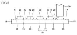
- FIG. 6 is a schematic cross-sectional view showing a step subsequent to the step shown in FIG.
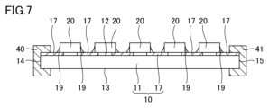
- FIG. 7 is a schematic cross-sectional view showing a step subsequent to the step shown in FIG. 6 in the manufacturing method of the chip resistor module according to the embodiment.
- FIG. 8 is a schematic cross-sectional view of a chip resistor module of a first modified example of the embodiment.
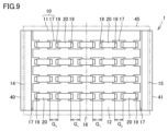
- FIG. 9 is a schematic plan view of a chip resistor module of a second modification of the embodiment.
- a chip resistor module 1 includes a wiring board 10 , a plurality of chip resistors 20 and a pair of terminal electrodes 40 and 41 .
- the chip resistor module 1 may further comprise an insulating sealing member 45 .
- the wiring board 10 is, for example, a printed circuit board.
- the wiring board 10 includes an insulating substrate 11 and electrical wiring 17 .
- the insulating substrate 11 is made of an electrically insulating material.
- the insulating substrate 11 is, for example, a glass epoxy substrate or a ceramic substrate (eg, alumina substrate).
- the insulating substrate 11 has a front surface 12 , a back surface 13 and side surfaces 14 and 15 . Each of side surfaces 14 and 15 is connected to front surface 12 and back surface 13 . Side 15 may be opposite side 14 .
- the longitudinal direction of the insulating substrate 11 may be the direction in which the side surfaces 14 and 15 are separated from each other.
- the electric wiring 17 is made of metal such as copper or aluminum, for example.
- the electric wiring 17 is provided on the insulating substrate 11 (for example, the front surface 12).
- the electric wiring 17 is formed, for example, by patterning a conductive film provided on the entire surface of the front surface 12 by etching or the like.
- a plurality of chip resistors 20 are joined to electrical wiring 17 using a conductive joining member 19 such as solder.
- a conductive joining member 19 such as solder.
- the plurality of chip resistors 20 are arranged two-dimensionally.
- the plurality of chip resistors 20 are arranged along the longitudinal direction of the insulating substrate 11 and the lateral direction of the insulating substrate 11 .
- the plurality of chip resistors 20 may be connected in series with each other, may be connected in parallel with each other, or may be connected in series and parallel with each other.
- each of the plurality of chip resistors 20 includes an insulating substrate 21, a pair of electrodes 30, and a resistor 27.
- Each of the multiple chip resistors 20 may further include an insulating protective layer 38 .
- the insulating substrate 21 is an electrical insulator and is made of an electrical insulating material such as alumina (Al 2 O 3 ).
- Insulating substrate 21 includes a first major surface 22 , a second major surface 23 opposite first major surface 22 , a side surface 24 and a side surface 25 opposite side surface 24 .
- Sides 24 and 25 are connected to first major surface 22 and second major surface 23, respectively.
- the longitudinal direction of the insulating substrate 21 is the direction in which the side surfaces 24 and 25 are separated from each other.
- the second major surface 23 may face the insulating substrate 11 (eg, the front surface 12).
- the resistor 27 has a function of limiting current or a function of detecting current.
- the resistor 27 is provided, for example, on the first major surface 22 of the insulating substrate 21 .
- the resistor 27 is formed by printing a paste of an electrically resistive material such as ruthenium oxide (RuO 2 ) or a silver-palladium alloy containing glass frit on the first main surface 22 of the insulating substrate 21 and baking the paste. formed by A trimming groove 28 is provided in the resistor 27 . By forming the trimming groove 28 in the resistor 27, the resistance value of each of the plurality of chip resistors 20 can be determined accurately.
- RuO 2 ruthenium oxide
- a trimming groove 28 is provided in the resistor 27 .
- One of the pair of electrodes 30 is provided on the side surface 24 of the insulating substrate 21 .
- One of the pair of electrodes 30 is closer to side 24 than to side 25 .
- the other of the pair of electrodes 30 is provided on the side surface 24 of the insulating substrate 21 .
- the other of the pair of electrodes 30 is closer to side 25 than to side 24 .
- Each of the pair of electrodes 30 includes, for example, a front electrode 31, a back electrode 32, a side electrode 33, and a metal plating layer .
- the front electrode 31 is provided on the first principal surface 22 .
- the front electrode 31 is in contact with the resistor 27 .
- the front electrode 31 is formed, for example, by printing a paste containing silver on the first main surface 22 of the insulating substrate 21 and firing the paste.
- the back electrode 32 is provided on the second main surface 23 .
- the back electrode 32 is formed, for example, by printing a paste containing silver on the second main surface 23 of the insulating substrate 21 and firing the paste.
- the side electrodes 33 are provided on the side surfaces 24 and 25, on the front surface electrode 31, and on the back surface electrode 32.
- the side electrode 33 is electrically connected to the front electrode 31 and the back electrode 32 .
- the side electrodes 33 are formed by applying a paste containing metal particles such as silver particles and resin such as epoxy resin to the side surfaces 24 and 25, the front electrode 31, and the back electrode 32. formed by
- the metal plating layer 34 is provided on the front electrode 31 , the back electrode 32 , and the side electrode 33 .
- the metal plating layer 34 includes, for example, an inner plating layer 35 and an outer plating layer 36 .
- the inner plating layer 35 is formed on the side electrode 33 and covers the side electrode 33 .
- the inner plating layer 35 protects the front electrode 31, the back electrode 32, and the side electrode 33 from heat and impact.
- the inner plating layer 35 is, for example, a nickel plating layer.
- the outer plating layer 36 is formed on the inner plating layer 35 and covers the inner plating layer 35 .
- the outer plated layer 36 is made of a material such as solder to which the conductive joining member 19 adheres more easily than the inner plated layer 35 .
- the outer plating layer 36 is, for example, a tin plating layer.
- the chip resistor 20 is mounted on the wiring board 10 with the conductive joining member 19 attached to the outer plating layer 36 and the electric wiring 17 of the wiring board
- the insulating protective layer 38 is provided on the resistor 27 .
- the insulating protective layer 38 electrically insulates the pair of electrodes 30 from each other.
- the insulating protective layer 38 is made of, for example, insulating resin such as epoxy resin.
- the insulating protective layer 38 is formed, for example, by printing and curing a paste containing an insulating resin.
- the insulating sealing member 45 seals the chip resistors 20 .
- the insulating sealing member 45 covers the chip resistors 20 , the front surface 12 of the insulating substrate 11 , and the electrical wiring 17 .
- the insulating sealing member 45 is made of, for example, an electrically insulating resin such as epoxy resin.
- the insulating sealing member 45 protects the plurality of chip resistors 20 from moisture and the like contained in the ambient atmosphere of the chip resistor module 1 .
- the insulating sealing member 45 may further cover the rear surface 13 of the insulating substrate 11 and part of each of the pair of terminal electrodes 40 and 41 .
- the insulating sealing member 45 may contact each of the pair of terminal electrodes 40 and 41 .
- a pair of terminal electrodes 40 and 41 are electrically connected to the electrical wiring 17 .
- the terminal electrodes 40 are provided on the electrical wiring 17 , the side surface 14 of the insulating substrate 11 , and the back surface 13 of the insulating substrate 11 .
- the terminal electrodes 41 are provided on the electrical wiring 17 , the side surface 15 of the insulating substrate 11 , and the back surface 13 of the insulating substrate 11 .
- Terminal electrodes 40 and 41 are made of a conductive material such as copper, aluminum or silver.
- the terminal electrodes 40, 41 may be lead frames made of metal such as copper or aluminum, for example.
- the terminal electrodes 40 and 41 are formed by applying a conductive paste containing metal particles such as silver particles to the electrical wiring 17, the side surfaces 14 and 15 of the insulating substrate 11, and the back surface 13 of the insulating substrate 11. may be formed. At least part of each of the terminal electrodes 40 and 41 is exposed from the insulating sealing member 45 . Each surface of the terminal electrodes 40 and 41 may be covered with a layer (for example, a tin layer) formed of a material such as solder to which a conductive joining member easily adheres.
- the chip resistor module 1 is, for example, a discharge resistor.
- a discharge resistor is connected in parallel with a capacitor (not shown).
- the discharge resistor discharges the voltage charged in the capacitor in a short period of time.
- a discharge resistor is used, for example, in a charge/discharge circuit for an electric vehicle or the like.
- the discharge resistor When the discharge resistor is continuously energized, the discharge resistor has a rated power of, for example, 5 W or more. If the discharge resistor is momentarily energized for a time of 10 seconds or less, the discharge resistor has a power rating of, for example, 20 W or more.
- the rated power means the upper limit of the power that the discharge resistor (chip resistor module 1) can consume without burning out the plurality of chip resistors 20 .
- the wiring substrate 10 is prepared by forming the electric wiring 17 on the insulating substrate 11 .
- the conductive film on the insulating substrate 11 is patterned by etching or the like to form the electric wiring 17 having a pattern suitable for the application of the chip resistor module 1 .
- a die bonder 50 is used to bond a plurality of chip resistors 20 to electrical wiring 17 .
- a plurality of chip resistors 20 are bonded to electrical wiring 17 using conductive bonding members 19 .
- a pair of terminal electrodes 40 and 41 electrically connected to the electric wiring 17 are provided.
- a lead frame as a pair of terminal electrodes 40 and 41 may be joined to the electrical wiring 17 using a conductive joining member 19 (not shown) such as solder.
- a pair of terminal electrodes 40, 41 are formed by applying a conductive paste containing metal particles, such as silver particles, over the electrical wiring 17, the side surfaces 14, 15, and the back surface 13. good too.
- an insulating sealing member 45 for sealing a plurality of chip resistors 20 is provided by compression molding, transfer molding, or the like. Thus, the chip resistor module 1 is obtained.
- the chip resistor module 1 of the first modified example of the present embodiment further includes a heat conductive sheet 43.
- the thermally conductive sheet 43 has higher thermal conductivity than the insulating sealing member 45 .
- the heat conductive sheet 43 has a heat conductivity of 0.5 W/(m ⁇ K) or more, for example. 5.
- the thermally conductive sheet 43 may have a thermal conductivity of 1.0 W/(m ⁇ K) or more, or may have a thermal conductivity of 3.0 W/(m ⁇ K) or more. It may have a thermal conductivity of 0 W/(m ⁇ K) or more.
- the heat-conducting sheet 43 is made of, for example, silicone-based resin.
- the thermally conductive sheet 43 covers the plurality of chip resistors 20 and has electrical insulation.
- the thermally conductive sheet 43 may contact the electrical wiring 17 .
- the thermally conductive sheet 43 may contact the pair of terminal electrodes 40 and 41 .
- a thermally conductive sheet 43 is arranged between the plurality of chip resistors 20 and the insulating sealing member 45 .
- the insulating sealing member 45 covers the heat conductive sheet 43 .
- the interval G 1 is the interval between a pair of first chip resistors among the plurality of chip resistors 20 that are adjacent to each other in the direction in which the pair of terminal electrodes 40 and 41 are separated from each other.
- the interval G 2 is the interval between a pair of second chip resistors among the plurality of chip resistors 20 that are adjacent to each other in the direction in which the pair of terminal electrodes 40 and 41 are separated from each other.
- the pair of first chip resistors are arranged closer to the center 16 of the insulating substrate 11 than the pair of second chip resistors in the direction in which the pair of terminal electrodes 40 and 41 are separated from each other. Spacing G 1 is greater than spacing G 2 .
- a chip resistor module 1 of this embodiment includes a wiring substrate 10 , a plurality of chip resistors 20 , and a pair of terminal electrodes 40 and 41 .
- the wiring board 10 includes an insulating substrate 11 and electrical wiring 17 provided on the insulating substrate 11 .
- a plurality of chip resistors 20 are joined to the electrical wiring 17 .
- a pair of terminal electrodes 40 and 41 are electrically connected to the electrical wiring 17 .
- the chip resistor module 1 the plurality of chip resistors 20, the wiring substrate 10, and the pair of terminal electrodes 40, 41 are modularized. Therefore, the chip resistor module 1 can be mounted on a circuit board (not shown) using a mounter (not shown). Moreover, by changing the number of the plurality of chip resistors 20 or the pattern of the electrical wiring 17, the chip resistor module 1 having specifications (for example, resistance value or rated power) suitable for the application of the chip resistor module 1 can be easily obtained. Thus, it is possible to provide the chip resistor module 1 with improved usability for the user.
- the chip resistor module 1 is obtained by a simpler process of attaching a plurality of chip resistors 20 and a pair of terminal electrodes 40 and 41 to the wiring board 10 .
- Chip resistor module 1 can be assembled using a machine such as die bonder 50 . The cost of the chip resistor module 1 can be reduced.
- the chip resistor module 1 can be miniaturized.
- the pair of chip resistors 20 adjacent to each other is increased.
- the center 16 of the insulating substrate 11 is the portion of the insulating substrate 11 that is farthest from the pair of terminal electrodes 40 and 41 . Therefore, the temperature of the chip resistor 20 tends to rise as the center 16 of the insulating substrate 11 is approached.
- the chip resistor module 1 of the present embodiment the temperature rise of the chip resistors 20 near the center 16 of the insulating substrate 11 can be suppressed. Therefore, the rated power of the chip resistor module 1 can be increased. The life of the chip resistor module 1 can be extended. It is possible to provide the chip resistor module 1 with improved usability for the user.
- the chip resistor module 1 of this embodiment further includes an insulating sealing member 45 that seals the plurality of chip resistors 20 .
- the insulating sealing member 45 protects the plurality of chip resistors 20 from moisture contained in the ambient atmosphere of the chip resistor module 1 . Therefore, the life of the chip resistor module 1 can be extended. It is possible to provide the chip resistor module 1 with improved usability for the user.
- the chip resistor module 1 of the present embodiment further includes a heat conductive sheet 43.
- the thermally conductive sheet 43 covers the plurality of chip resistors 20 and has electrical insulation.
- the heat-conducting sheet 43 quickly spreads the heat generated by the plurality of chip resistors 20 and allows the heat to escape efficiently to the outside of the chip resistor module 1 through the pair of terminal electrodes 40 and 41. do. Temperature rise of the plurality of chip resistors 20 can be suppressed. Therefore, the rated power of the chip resistor module 1 can be increased. The life of the chip resistor module 1 can be extended.
- the chip resistor module 1 can be miniaturized. It is possible to provide the chip resistor module 1 with improved usability for the user.
- the heat conductive sheet 43 is in contact with the pair of terminal electrodes 40 and 41 .
- the heat-conducting sheet 43 quickly transfers heat generated by the plurality of chip resistors 20 to the pair of terminal electrodes 40 and 41, and efficiently transfers the heat to the outside of the chip resistor module 1 through the pair of terminal electrodes 40 and 41. allow to escape. Therefore, the rated power of the chip resistor module 1 can be increased. The life of the chip resistor module 1 can be extended.
- the chip resistor module 1 can be miniaturized. It is possible to provide the chip resistor module 1 with improved usability for the user.
- the insulating substrate 11 has a front surface 12, a back surface 13, and side surfaces 14 and 15 connected to the front surface 12 and the back surface 13. ing.
- An electric wiring 17 is formed on the front surface 12 .
- a pair of terminal electrodes 40 and 41 are provided on the electrical wiring 17 , the side surfaces 14 and 15 and the rear surface 13 .
- the insulating substrate 11 has a front surface 12 .
- An electric wiring 17 is formed on the front surface 12 .
- the plurality of chip resistors 20 are arranged two-dimensionally.
- the size of the chip resistor module 1 can be reduced. It is possible to provide the chip resistor module 1 with improved usability for the user.
- the chip resistor module 1 of this embodiment is a discharge resistor. It is possible to provide a discharge resistor with improved usability for the user. The cost of discharge resistors can be reduced. A discharge resistor can be miniaturized.
- 1 chip resistor module 10 wiring substrate, 11 insulating substrate, 12 front surface, 13 back surface, 14, 15 side surface, 16 center, 17 electrical wiring, 19 conductive joining member, 20 chip resistor, 21 insulating substrate, 22 First main surface, 23 Second main surface, 24, 25 Side surface, 27 Resistor, 28 Trimming groove, 30 Electrode, 31 Front electrode, 32 Back electrode, 33 Side electrode, 34 Metal plating layer, 35 Inner plating Layer, 36 Outer plating layer, 38 Insulation protection layer, 40, 41 Terminal electrode, 43 Thermal conductive sheet, 45 Insulation sealing member, 50 Die bonder.
Landscapes
- Engineering & Computer Science (AREA)
- Microelectronics & Electronic Packaging (AREA)
- Manufacturing & Machinery (AREA)
- Physics & Mathematics (AREA)
- Electromagnetism (AREA)
- Details Of Resistors (AREA)
Priority Applications (3)
| Application Number | Priority Date | Filing Date | Title |
|---|---|---|---|
| JP2023562147A JPWO2023089899A1 (https=) | 2021-11-18 | 2022-08-29 | |
| CN202280076382.9A CN118266044A (zh) | 2021-11-18 | 2022-08-29 | 片式电阻器模块 |
| US18/598,969 US20240212888A1 (en) | 2021-11-18 | 2024-03-07 | Chip resistor module |
Applications Claiming Priority (2)
| Application Number | Priority Date | Filing Date | Title |
|---|---|---|---|
| JP2021187678 | 2021-11-18 | ||
| JP2021-187678 | 2021-11-18 |
Related Child Applications (1)
| Application Number | Title | Priority Date | Filing Date |
|---|---|---|---|
| US18/598,969 Continuation US20240212888A1 (en) | 2021-11-18 | 2024-03-07 | Chip resistor module |
Publications (1)
| Publication Number | Publication Date |
|---|---|
| WO2023089899A1 true WO2023089899A1 (ja) | 2023-05-25 |
Family
ID=86396640
Family Applications (1)
| Application Number | Title | Priority Date | Filing Date |
|---|---|---|---|
| PCT/JP2022/032394 Ceased WO2023089899A1 (ja) | 2021-11-18 | 2022-08-29 | チップ抵抗器モジュール |
Country Status (4)
| Country | Link |
|---|---|
| US (1) | US20240212888A1 (https=) |
| JP (1) | JPWO2023089899A1 (https=) |
| CN (1) | CN118266044A (https=) |
| WO (1) | WO2023089899A1 (https=) |
Cited By (1)
| Publication number | Priority date | Publication date | Assignee | Title |
|---|---|---|---|---|
| TWI876614B (zh) * | 2023-10-24 | 2025-03-11 | 天二科技股份有限公司 | 晶片電阻及其製造方法 |
Citations (4)
| Publication number | Priority date | Publication date | Assignee | Title |
|---|---|---|---|---|
| JPH0963805A (ja) * | 1995-08-28 | 1997-03-07 | Matsushita Electric Ind Co Ltd | 角形チップ抵抗器 |
| JP2002075702A (ja) * | 2000-08-25 | 2002-03-15 | K-Tech Devices Corp | 面実装型ネットワーク電子部品及びその製造法 |
| JP2011041363A (ja) * | 2009-08-07 | 2011-02-24 | Hitachi Automotive Systems Ltd | 直流電源平滑用コンデンサーの放電回路 |
| WO2019116814A1 (ja) * | 2017-12-11 | 2019-06-20 | パナソニックIpマネジメント株式会社 | チップ抵抗器 |
-
2022
- 2022-08-29 JP JP2023562147A patent/JPWO2023089899A1/ja active Pending
- 2022-08-29 WO PCT/JP2022/032394 patent/WO2023089899A1/ja not_active Ceased
- 2022-08-29 CN CN202280076382.9A patent/CN118266044A/zh active Pending
-
2024
- 2024-03-07 US US18/598,969 patent/US20240212888A1/en active Pending
Patent Citations (4)
| Publication number | Priority date | Publication date | Assignee | Title |
|---|---|---|---|---|
| JPH0963805A (ja) * | 1995-08-28 | 1997-03-07 | Matsushita Electric Ind Co Ltd | 角形チップ抵抗器 |
| JP2002075702A (ja) * | 2000-08-25 | 2002-03-15 | K-Tech Devices Corp | 面実装型ネットワーク電子部品及びその製造法 |
| JP2011041363A (ja) * | 2009-08-07 | 2011-02-24 | Hitachi Automotive Systems Ltd | 直流電源平滑用コンデンサーの放電回路 |
| WO2019116814A1 (ja) * | 2017-12-11 | 2019-06-20 | パナソニックIpマネジメント株式会社 | チップ抵抗器 |
Cited By (1)
| Publication number | Priority date | Publication date | Assignee | Title |
|---|---|---|---|---|
| TWI876614B (zh) * | 2023-10-24 | 2025-03-11 | 天二科技股份有限公司 | 晶片電阻及其製造方法 |
Also Published As
| Publication number | Publication date |
|---|---|
| US20240212888A1 (en) | 2024-06-27 |
| CN118266044A (zh) | 2024-06-28 |
| JPWO2023089899A1 (https=) | 2023-05-25 |
Similar Documents
| Publication | Publication Date | Title |
|---|---|---|
| JP3640146B2 (ja) | 保護素子 | |
| TWI500063B (zh) | 包含電阻及熔線元件之電路保護裝置 | |
| JP2004265618A (ja) | 保護素子 | |
| US20070195066A1 (en) | Temperature sensor and method for its production | |
| JPH0760761B2 (ja) | フィルム型の電力用抵抗器組立体 | |
| WO2023089899A1 (ja) | チップ抵抗器モジュール | |
| JPH09148053A (ja) | セラミックヒータ | |
| JP2003282301A (ja) | チップ抵抗器およびその製造方法 | |
| US7205878B2 (en) | Over-current protection device and manufacturing method thereof | |
| KR19980018524A (ko) | 최소한 한 금속-적층을 가진 기판의 제조방법 및 프린트기판과 그의 적용 | |
| JPH09320802A (ja) | 抵抗器 | |
| JP2008270325A (ja) | 静電気対策部品およびこれを用いた発光ダイオードモジュール | |
| EP3703139B1 (en) | Thermoelectric module | |
| KR101075664B1 (ko) | 칩 저항기 및 이의 제조 방법 | |
| EP1615239B1 (en) | power resistor having a heat generating resistive element | |
| JP2008227137A (ja) | 静電気対策部品およびこれを用いた発光ダイオードモジュール | |
| CN209929256U (zh) | 具有高导热基板的大电流熔断器 | |
| CN101800102A (zh) | 过电流保护组件及其制造方法 | |
| WO2022091644A1 (ja) | チップ抵抗器 | |
| JP3549230B2 (ja) | 回路構成体とその製造方法 | |
| JP4777764B2 (ja) | 温度補償回路基板の製造方法 | |
| CN110211852B (zh) | 具有高导热基板的大电流熔断器及其制作方法 | |
| JPS637601A (ja) | 面実装用ネツトワ−ク抵抗器 | |
| JPH07211509A (ja) | チップ抵抗器とその製造方法 | |
| JPH1196872A (ja) | 複合回路素子 |
Legal Events
| Date | Code | Title | Description |
|---|---|---|---|
| 121 | Ep: the epo has been informed by wipo that ep was designated in this application |
Ref document number: 22895187 Country of ref document: EP Kind code of ref document: A1 |
|
| WWE | Wipo information: entry into national phase |
Ref document number: 2023562147 Country of ref document: JP |
|
| WWE | Wipo information: entry into national phase |
Ref document number: 202280076382.9 Country of ref document: CN |
|
| 122 | Ep: pct application non-entry in european phase |
Ref document number: 22895187 Country of ref document: EP Kind code of ref document: A1 |