WO2023079398A1 - 半導体装置、及び電子機器 - Google Patents
半導体装置、及び電子機器 Download PDFInfo
- Publication number
- WO2023079398A1 WO2023079398A1 PCT/IB2022/060118 IB2022060118W WO2023079398A1 WO 2023079398 A1 WO2023079398 A1 WO 2023079398A1 IB 2022060118 W IB2022060118 W IB 2022060118W WO 2023079398 A1 WO2023079398 A1 WO 2023079398A1
- Authority
- WO
- WIPO (PCT)
- Prior art keywords
- transistor
- insulator
- conductor
- oxide
- metal oxide
- Prior art date
- Legal status (The legal status is an assumption and is not a legal conclusion. Google has not performed a legal analysis and makes no representation as to the accuracy of the status listed.)
- Ceased
Links
Images























Classifications
-
- H—ELECTRICITY
- H10—SEMICONDUCTOR DEVICES; ELECTRIC SOLID-STATE DEVICES NOT OTHERWISE PROVIDED FOR
- H10B—ELECTRONIC MEMORY DEVICES
- H10B12/00—Dynamic random access memory [DRAM] devices
-
- H—ELECTRICITY
- H10—SEMICONDUCTOR DEVICES; ELECTRIC SOLID-STATE DEVICES NOT OTHERWISE PROVIDED FOR
- H10D—INORGANIC ELECTRIC SEMICONDUCTOR DEVICES
- H10D84/00—Integrated devices formed in or on semiconductor substrates that comprise only semiconducting layers, e.g. on Si wafers or on GaAs-on-Si wafers
- H10D84/01—Manufacture or treatment
- H10D84/0123—Integrating together multiple components covered by H10D12/00 or H10D30/00, e.g. integrating multiple IGBTs
- H10D84/0126—Integrating together multiple components covered by H10D12/00 or H10D30/00, e.g. integrating multiple IGBTs the components including insulated gates, e.g. IGFETs
-
- H—ELECTRICITY
- H10—SEMICONDUCTOR DEVICES; ELECTRIC SOLID-STATE DEVICES NOT OTHERWISE PROVIDED FOR
- H10D—INORGANIC ELECTRIC SEMICONDUCTOR DEVICES
- H10D84/00—Integrated devices formed in or on semiconductor substrates that comprise only semiconducting layers, e.g. on Si wafers or on GaAs-on-Si wafers
- H10D84/80—Integrated devices formed in or on semiconductor substrates that comprise only semiconducting layers, e.g. on Si wafers or on GaAs-on-Si wafers characterised by the integration of at least one component covered by groups H10D12/00 or H10D30/00, e.g. integration of IGFETs
- H10D84/82—Integrated devices formed in or on semiconductor substrates that comprise only semiconducting layers, e.g. on Si wafers or on GaAs-on-Si wafers characterised by the integration of at least one component covered by groups H10D12/00 or H10D30/00, e.g. integration of IGFETs of only field-effect components
- H10D84/83—Integrated devices formed in or on semiconductor substrates that comprise only semiconducting layers, e.g. on Si wafers or on GaAs-on-Si wafers characterised by the integration of at least one component covered by groups H10D12/00 or H10D30/00, e.g. integration of IGFETs of only field-effect components of only insulated-gate FETs [IGFET]
- H10D84/85—Complementary IGFETs, e.g. CMOS
-
- H—ELECTRICITY
- H10—SEMICONDUCTOR DEVICES; ELECTRIC SOLID-STATE DEVICES NOT OTHERWISE PROVIDED FOR
- H10D—INORGANIC ELECTRIC SEMICONDUCTOR DEVICES
- H10D30/00—Field-effect transistors [FET]
- H10D30/01—Manufacture or treatment
- H10D30/021—Manufacture or treatment of FETs having insulated gates [IGFET]
-
- H—ELECTRICITY
- H10—SEMICONDUCTOR DEVICES; ELECTRIC SOLID-STATE DEVICES NOT OTHERWISE PROVIDED FOR
- H10D—INORGANIC ELECTRIC SEMICONDUCTOR DEVICES
- H10D30/00—Field-effect transistors [FET]
- H10D30/60—Insulated-gate field-effect transistors [IGFET]
- H10D30/67—Thin-film transistors [TFT]
- H10D30/674—Thin-film transistors [TFT] characterised by the active materials
- H10D30/6755—Oxide semiconductors, e.g. zinc oxide, copper aluminium oxide or cadmium stannate
-
- H—ELECTRICITY
- H10—SEMICONDUCTOR DEVICES; ELECTRIC SOLID-STATE DEVICES NOT OTHERWISE PROVIDED FOR
- H10D—INORGANIC ELECTRIC SEMICONDUCTOR DEVICES
- H10D30/00—Field-effect transistors [FET]
- H10D30/60—Insulated-gate field-effect transistors [IGFET]
- H10D30/67—Thin-film transistors [TFT]
- H10D30/6757—Thin-film transistors [TFT] characterised by the structure of the channel, e.g. transverse or longitudinal shape or doping profile
-
- H—ELECTRICITY
- H10—SEMICONDUCTOR DEVICES; ELECTRIC SOLID-STATE DEVICES NOT OTHERWISE PROVIDED FOR
- H10D—INORGANIC ELECTRIC SEMICONDUCTOR DEVICES
- H10D84/00—Integrated devices formed in or on semiconductor substrates that comprise only semiconducting layers, e.g. on Si wafers or on GaAs-on-Si wafers
-
- H—ELECTRICITY
- H10—SEMICONDUCTOR DEVICES; ELECTRIC SOLID-STATE DEVICES NOT OTHERWISE PROVIDED FOR
- H10D—INORGANIC ELECTRIC SEMICONDUCTOR DEVICES
- H10D84/00—Integrated devices formed in or on semiconductor substrates that comprise only semiconducting layers, e.g. on Si wafers or on GaAs-on-Si wafers
- H10D84/01—Manufacture or treatment
- H10D84/0123—Integrating together multiple components covered by H10D12/00 or H10D30/00, e.g. integrating multiple IGBTs
- H10D84/0126—Integrating together multiple components covered by H10D12/00 or H10D30/00, e.g. integrating multiple IGBTs the components including insulated gates, e.g. IGFETs
- H10D84/0165—Integrating together multiple components covered by H10D12/00 or H10D30/00, e.g. integrating multiple IGBTs the components including insulated gates, e.g. IGFETs the components including complementary IGFETs, e.g. CMOS devices
-
- H—ELECTRICITY
- H10—SEMICONDUCTOR DEVICES; ELECTRIC SOLID-STATE DEVICES NOT OTHERWISE PROVIDED FOR
- H10D—INORGANIC ELECTRIC SEMICONDUCTOR DEVICES
- H10D84/00—Integrated devices formed in or on semiconductor substrates that comprise only semiconducting layers, e.g. on Si wafers or on GaAs-on-Si wafers
- H10D84/01—Manufacture or treatment
- H10D84/02—Manufacture or treatment characterised by using material-based technologies
- H10D84/03—Manufacture or treatment characterised by using material-based technologies using Group IV technology, e.g. silicon technology or silicon-carbide [SiC] technology
- H10D84/038—Manufacture or treatment characterised by using material-based technologies using Group IV technology, e.g. silicon technology or silicon-carbide [SiC] technology using silicon technology, e.g. SiGe
-
- H—ELECTRICITY
- H10—SEMICONDUCTOR DEVICES; ELECTRIC SOLID-STATE DEVICES NOT OTHERWISE PROVIDED FOR
- H10D—INORGANIC ELECTRIC SEMICONDUCTOR DEVICES
- H10D84/00—Integrated devices formed in or on semiconductor substrates that comprise only semiconducting layers, e.g. on Si wafers or on GaAs-on-Si wafers
- H10D84/01—Manufacture or treatment
- H10D84/02—Manufacture or treatment characterised by using material-based technologies
- H10D84/08—Manufacture or treatment characterised by using material-based technologies using combinations of technologies, e.g. using both Si and SiC technologies or using both Si and Group III-V technologies
-
- H—ELECTRICITY
- H10—SEMICONDUCTOR DEVICES; ELECTRIC SOLID-STATE DEVICES NOT OTHERWISE PROVIDED FOR
- H10D—INORGANIC ELECTRIC SEMICONDUCTOR DEVICES
- H10D84/00—Integrated devices formed in or on semiconductor substrates that comprise only semiconducting layers, e.g. on Si wafers or on GaAs-on-Si wafers
- H10D84/80—Integrated devices formed in or on semiconductor substrates that comprise only semiconducting layers, e.g. on Si wafers or on GaAs-on-Si wafers characterised by the integration of at least one component covered by groups H10D12/00 or H10D30/00, e.g. integration of IGFETs
- H10D84/82—Integrated devices formed in or on semiconductor substrates that comprise only semiconducting layers, e.g. on Si wafers or on GaAs-on-Si wafers characterised by the integration of at least one component covered by groups H10D12/00 or H10D30/00, e.g. integration of IGFETs of only field-effect components
- H10D84/83—Integrated devices formed in or on semiconductor substrates that comprise only semiconducting layers, e.g. on Si wafers or on GaAs-on-Si wafers characterised by the integration of at least one component covered by groups H10D12/00 or H10D30/00, e.g. integration of IGFETs of only field-effect components of only insulated-gate FETs [IGFET]
-
- H—ELECTRICITY
- H10—SEMICONDUCTOR DEVICES; ELECTRIC SOLID-STATE DEVICES NOT OTHERWISE PROVIDED FOR
- H10B—ELECTRONIC MEMORY DEVICES
- H10B41/00—Electrically erasable-and-programmable ROM [EEPROM] devices comprising floating gates
- H10B41/70—Electrically erasable-and-programmable ROM [EEPROM] devices comprising floating gates the floating gate being an electrode shared by two or more components
-
- H—ELECTRICITY
- H10—SEMICONDUCTOR DEVICES; ELECTRIC SOLID-STATE DEVICES NOT OTHERWISE PROVIDED FOR
- H10D—INORGANIC ELECTRIC SEMICONDUCTOR DEVICES
- H10D30/00—Field-effect transistors [FET]
- H10D30/60—Insulated-gate field-effect transistors [IGFET]
- H10D30/67—Thin-film transistors [TFT]
- H10D30/6729—Thin-film transistors [TFT] characterised by the electrodes
- H10D30/673—Thin-film transistors [TFT] characterised by the electrodes characterised by the shapes, relative sizes or dispositions of the gate electrodes
- H10D30/6733—Multi-gate TFTs
- H10D30/6734—Multi-gate TFTs having gate electrodes arranged on both top and bottom sides of the channel, e.g. dual-gate TFTs
Definitions
- One embodiment of the present invention relates to semiconductor devices and electronic devices.
- one embodiment of the present invention is not limited to the above technical field.
- Technical fields of one embodiment of the present invention disclosed in this specification and the like include semiconductor devices, display devices, light-emitting devices, power storage devices, memory devices, electronic devices, lighting devices, input devices, input/output devices, and driving methods thereof. , or methods for producing them, can be mentioned as an example.
- a CPU Central Processing Units
- a CPU is an aggregate of semiconductor elements having integrated circuits (at least transistors and memories) chipped by processing a semiconductor wafer and having electrodes as connection terminals.
- Integrated circuits such as LSIs, CPUs, and memories are mounted on circuit boards, such as printed wiring boards, and used as one of the components of various electronic devices.
- a technique for forming a transistor using a semiconductor thin film formed on a substrate having an insulating surface is attracting attention.
- the transistor is widely applied to electronic devices such as integrated circuits and image display devices (also simply referred to as display devices).
- Silicon-based semiconductor materials are widely known as semiconductor thin films applicable to transistors, but oxide semiconductors are attracting attention as other materials.
- Patent Document 1 discloses a low power consumption CPU that utilizes a characteristic of a transistor including an oxide semiconductor that leakage current is small.
- Patent Document 2 discloses a memory device that can retain stored data for a long period of time by taking advantage of the low leakage current characteristic of a transistor including an oxide semiconductor.
- An object of one embodiment of the present invention is to provide a miniaturized semiconductor device. Alternatively, an object of one embodiment of the present invention is to provide a highly reliable semiconductor device. Alternatively, an object of one embodiment of the present invention is to provide a novel semiconductor device.
- One aspect of the present invention has a first layer and a second layer on the first layer, the first layer having silicon in a first channel forming region of a p-channel type a first transistor, the second layer having an n-channel second transistor having a metal oxide in the second channel-forming region, the first transistor and the second transistor; , and the channel length of the first transistor is longer than the channel length of the second transistor.
- the channel length of the first transistor may be 15 nm or more, and the channel length of the second transistor may be less than 15 nm.
- the first transistor may have a channel length of 15 nm or more and 40 nm or less
- the second transistor may have a channel length of 3 nm or more and less than 15 nm.
- the first layer may have a single crystal silicon substrate, and the first transistor may have a first channel formation region in the single crystal silicon substrate.
- the second layer may comprise memory circuitry.
- the memory circuit includes a third transistor, a fourth transistor, and a capacitor, and one of the source and drain of the third transistor is electrically connected to the gate of the fourth transistor. , and the gate of the fourth transistor may be electrically connected to one electrode of the capacitor.
- the third transistor and the fourth transistor may have metal oxide in the second channel formation region.
- An electronic device including a semiconductor device of one embodiment of the present invention and a display portion is also one embodiment of the present invention.
- a miniaturized semiconductor device can be provided.
- a highly reliable semiconductor device can be provided.
- one embodiment of the present invention can provide a novel semiconductor device.
- FIG. 1 is a block diagram showing a configuration example of a semiconductor device.
- FIG. 2 is a perspective view showing a configuration example of a semiconductor device.
- FIG. 3 is a circuit diagram showing a configuration example of a CMOS circuit.
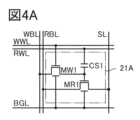
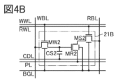
- 4A to 4H are circuit diagrams showing configuration examples of memory circuits.
- FIG. 5 is a perspective view showing a configuration example of a semiconductor device.
- FIG. 6 is a circuit diagram showing a configuration example of a memory circuit.
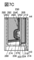
- FIG. 7A is a top view showing a configuration example of a transistor.
- 7B to 7D are cross-sectional views showing configuration examples of transistors.
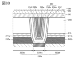
- 8A and 8B are cross-sectional views showing configuration examples of transistors.
- FIG. 9 is a cross-sectional view showing a configuration example of a transistor.
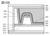
- FIG. 10A and 10B are cross-sectional views showing configuration examples of transistors.
- 11A and 11B are cross-sectional views showing configuration examples of transistors.
- 12A and 12B are cross-sectional views showing configuration examples of transistors.
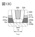
- 13A to 13F are cross-sectional views showing configuration examples of transistors.
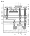
- FIG. 14 is a cross-sectional view showing a configuration example of a semiconductor device.
- FIG. 15 is a cross-sectional view showing a configuration example of a semiconductor device.
- FIG. 16 is a cross-sectional view showing a configuration example of a semiconductor device.
- FIG. 17 is a cross-sectional view showing a configuration example of a semiconductor device.
- FIG. 18 is a cross-sectional view showing a configuration example of a semiconductor device.
- FIG. 15 is a cross-sectional view showing a configuration example of a semiconductor device.
- FIG. 16 is a cross-sectional view showing a configuration example of a semiconductor device.
- FIG. 17 is
- FIG. 19 is a cross-sectional view showing a configuration example of a semiconductor device.
- FIG. 20 is a cross-sectional view showing a configuration example of a semiconductor device.
- 21A and 21B are block diagrams showing configuration examples of semiconductor devices.
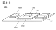
- 22A and 22B are diagrams showing examples of electronic components.
- 23A to 23E are diagrams showing examples of storage devices.
- 24A to 24H are diagrams illustrating examples of electronic devices.
- 25A and 25B are diagrams showing changes in power consumption of a normally-off processor.
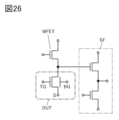
- FIG. 26 is a diagram showing a measurement circuit.
- FIG. 27 is a diagram showing the temperature dependence of off current.
- ordinal numbers such as “first” and “second” in this specification etc. are attached to avoid confusion of constituent elements, and do not indicate any order or ranking such as the order of steps or the order of stacking. do not have.
- ordinal numbers such as “first” and “second” in this specification etc. are attached to avoid confusion of constituent elements, and do not indicate any order or ranking such as the order of steps or the order of stacking. do not have.
- in order to avoid confusion between constituent elements even a term that is not given an ordinal number in this specification etc. may be given an ordinal number in the scope of claims.
- even a term is given an ordinal number in this specification etc., it may be given a different ordinal number in the scope of claims.
- the ordinal number may be omitted in the scope of claims even for a term that is attached with an ordinal number in this specification.
- off-state current refers to drain current when a transistor is in an off state (also referred to as a non-conducting state or a cutoff state).
- an off state means a state in which the voltage Vgs between the gate and the source is lower than the threshold voltage Vth in an n-channel transistor (higher than Vth in a p-channel transistor).
- a metal oxide is a metal oxide in a broad sense.
- Metal oxides are classified into oxide insulators, oxide conductors (including transparent oxide conductors), oxide semiconductors (also referred to as oxide semiconductors or simply OSs), and the like.
- oxide semiconductors also referred to as oxide semiconductors or simply OSs
- an OS transistor can be referred to as a transistor including a metal oxide or an oxide semiconductor.
- OSLSI oxide semiconductors
- An oxide semiconductor used for OSLSI contains at least indium (In) and oxygen (O). Typical examples include indium gallium zinc oxide (IGZO), indium zinc oxide (IZO (registered trademark)), and indium oxide (IO). Further, the oxide semiconductor may contain hydrogen as an impurity.
- IGZO indium gallium zinc oxide
- IZO indium zinc oxide
- IO indium oxide
- the oxide semiconductor may contain hydrogen as an impurity.
- One aspect of the present invention relates to a semiconductor device having a first layer and a second layer over the first layer.
- a transistor including silicon in a channel formation region (hereinafter also referred to as a Si transistor or SiFET) is provided in the first layer.
- the first layer can have a single crystal silicon substrate, and the Si transistor can have a channel forming region in the single crystal silicon substrate.
- the second layer is provided with a transistor including a metal oxide in a channel formation region (hereinafter also referred to as an OS transistor or an OSFET).
- a transistor including single crystal silicon in a channel formation region is referred to as a single crystal Si transistor.
- a transistor having a channel formation region in a single crystal silicon substrate is a single crystal Si transistor.
- the first transistor which is a p-channel Si transistor provided in the first layer and the second transistor which is an n-channel OS transistor provided in the second layer are provided. and a CMOS (Complementary Metal Oxide Semiconductor) circuit.
- CMOS Complementary Metal Oxide Semiconductor
- the mobility of a Si transistor such as a single-crystal Si transistor is higher than that of an OS transistor.
- the CMOS circuit may not operate normally.
- the channel length of the first transistor which is a Si transistor is made longer than the channel length of the second transistor which is an OS transistor.
- the longer the channel length the higher the electrical resistance between the source and the drain and the lower the mobility.
- the difference in mobility between the first transistor and the second transistor can be made smaller than when the second transistor has the same channel length. Therefore, since the difference between the ON currents of the first transistor and the second transistor can be reduced, even if the CMOS circuit is configured with the first transistor that is a Si transistor and the second transistor that is an OS transistor, The CMOS circuit can be driven normally.
- the channel length of the first transistor is 15 nm or more and the channel length of the second transistor is less than 15 nm.
- the channel length of the first transistor be 15 nm or more and 40 nm or less, and the channel length of the second transistor be 3 nm or more and less than 15 nm.
- the channel length of the second transistor can be typically 5 nm or more and 8 nm or less.
- the off-state current (Ioff) of the second transistor is 4% lower than that of the first transistor (SiFET). It can be designed to be ⁇ 5 orders of magnitude lower. With this design, it is possible to reduce the on-current (Ion).
- a semiconductor device of one embodiment of the present invention includes a memory portion, and memory circuits are arranged in a matrix in the memory portion.
- the memory circuit has a write transistor, a read transistor, and a select transistor.
- one of the source and drain of the write transistor is electrically connected to the gate of the read transistor
- one of the source and drain of the read transistor is electrically connected to one of the source and drain of the select transistor.
- the write transistor functions as a switch that controls writing and holding of data in the memory circuit. Data is written in the memory circuit by turning on the writing transistor, and data is held in the memory circuit by turning off the writing transistor.
- the reading transistor has a function of amplifying and reading data held in the memory circuit.
- the selection transistor functions as a switch that selects a memory circuit from which data is read. By turning on the selection transistor, data held in the memory circuit is read. Specifically, by turning on the selection transistor, a current corresponding to the data held in the memory circuit flows between the drain and source of the read transistor and the selection transistor, thereby amplifying and reading the data.
- a transistor with a low off-state current As the writing transistor because data can be held in the memory circuit for a long time.
- An OS transistor can be given as such a transistor.
- a transistor with a large on-state current as the reading transistor and the selection transistor because data can be read from the memory circuit at high speed.
- An example of such a transistor is a Si transistor.
- the read transistor and the selection transistor are provided in the first layer provided with the Si transistor, and the write transistor is provided in the second layer provided with the OS transistor. Data can be read out from the memory circuit at high speed.
- the writing transistor, the reading transistor, and the selection transistor can all be n-channel transistors.
- the potential supplied to the gate of the transistor functioning as a switch is the same as that of the transistor. It should be different for each type. For example, when a write transistor that is an OS transistor functioning as a switch is turned on, the potential supplied to the gate of the write transistor is changed to the potential supplied to the gate of the write transistor when turning on a selection transistor that is a Si transistor that functions as a switch. must be higher than the potential supplied to the gate of
- the channel length of the Si transistor provided in the first layer is longer than the channel length of the OS transistor provided in the second layer. Accordingly, the potential supplied to the gate of the Si transistor functioning as a switch when turning on the Si transistor and the potential supplied to the gate of the OS transistor functioning as a switch when turning on the OS transistor are obtained. , can be made equal. a potential supplied to the gate of the Si transistor functioning as a switch when the Si transistor is turned off; a potential supplied to the gate of the OS transistor functioning as a switch when the OS transistor is turned off; can be made equal. Therefore, the gate potential of the Si transistor functioning as a switch and the gate potential of the OS transistor functioning as a switch can be supplied from the same power supply.
- the degree of integration of the transistors in the second layer is equal to the degree of integration of the transistors in the first layer.
- the degree of integration of transistors in the second layer can be made smaller than the degree of integration of transistors in the first layer.
- FIG. 1 is a block diagram showing a configuration example of a semiconductor device 10 according to one aspect of the present invention.
- the semiconductor device 10 has a storage section 20 , a word line drive circuit 31 , a bit line drive circuit 32 , a control circuit 33 , a communication circuit 34 and an input/output circuit 35 .
- Memory circuits 21 are arranged in a matrix in the storage unit 20 .
- the memory circuit 21 functions as a memory element.
- a semiconductor device including a memory portion may be referred to as a memory device.
- the semiconductor device 10 can also be called a memory device.
- DRAM Dynamic Random Access Memory
- SRAM Static Random Access Memory
- phase change memory PCM: Phase-Change Memory
- Resistance change memory Resistive Random Access Memory
- MRAM Magnetoresistive Random Access Memory
- FeRAM Ferroelectric Random Access Memory
- Antiferroelectric Memory or the like may be used.
- NOSRAM Nonvolite Oxide Semiconductor Random Access Memory
- DOSRAM Dynamic Oxide Semiconductor Random Access Memory
- NOSRAM Nonvolatile Oxide Semiconductor Random Access Memory
- RAM Nonvolatile Oxide Semiconductor Random Access Memory
- NOSRAM refers to a memory in which the memory circuit is a two-transistor (2T) or three-transistor (3T) gain cell and the access transistor is an OS transistor. The current flowing between the source and the drain of the OS transistor in the off state, that is, the leak current is extremely small. The NOSRAM can read data without destroying it (non-destructive reading).
- DOSRAM (registered trademark) is an abbreviation for “Dynamic Oxide Semiconductor RAM” and refers to a RAM having a 1T (transistor) 1C (capacitor) type memory circuit.
- DOSRAM like NOSRAM, is a memory that utilizes the fact that the off-state current of an OS transistor is low.
- the word line driving circuit 31 is electrically connected to the memory circuit 21 via word lines.
- memory circuits 21 in the same row can be electrically connected to the same word line.
- the word line driving circuit 31 has a function of supplying signals to the memory circuit 21 for writing data and the memory circuit 21 for reading data. That is, the word line driving circuit 31 has a function of generating a selection signal, which is a signal for selecting the memory circuit 21 for writing data and the memory circuit 21 for reading data.
- the bit line driving circuit 32 is electrically connected to the memory circuit 21 via bit lines.
- memory circuits 21 in the same column can be electrically connected to the same bit line.
- the bit line drive circuit 32 has a function of generating data to be written in the memory circuit 21 . Specifically, the data generated by the bit line driving circuit 32 is written into the memory circuit 21 selected by the selection signal generated by the word line driving circuit 31 .
- the bit line driving circuit 32 also has a function of amplifying and reading data held in the memory circuit 21 . Specifically, the data held in the memory circuit 21 selected by the selection signal generated by the word line driving circuit 31 is amplified by the bit line driving circuit 32 and read out.
- the control circuit 33 has a function of controlling driving of the word line driving circuit 31 and the bit line driving circuit 32 . Specifically, the control circuit 33 processes a signal such as an enable signal supplied to the control circuit 33 from the outside of the semiconductor device 10 , and sends control signals to the word line driving circuit 31 and the bit line driving circuit 32 . can supply. Note that the control circuit 33 may have a function of controlling the driving of the communication circuit 34 and the input/output circuit 35 .
- the control circuit 33 can have a CPU, for example.
- the communication circuit 34 has a function of communicating wirelessly or by wire.
- having a function of wireless communication is preferable because the number of components such as cables for connection can be omitted.
- the communication circuit 34 can communicate via an antenna.
- LTE Long Term Evolution
- GSM Global System for Mobile Communication: registered trademark
- EDGE Enhanced Data Rates for GSM Evolution
- CDMA2000 Code Division Mu ltiple Access 2000
- W-CDMA registered trademark
- IEEE specifications standardized by IEEE such as Wi-Fi (registered trademark), Bluetooth (registered trademark), or ZigBee (registered trademark).
- the communication circuit 34 includes the Internet, intranet, extranet, PAN (Personal Area Network), LAN (Local Area Network), CAN (Campus Area Network), MAN (Metropolitan Area Network), Information can be input/output by connecting the semiconductor device 10 to other devices via a computer network such as WAN (Wide Area Network) or GAN (Global Area Network).
- PAN Personal Area Network
- LAN Local Area Network
- CAN Campus Area Network
- MAN Metropolitan Area Network
- Information can be input/output by connecting the semiconductor device 10 to other devices via a computer network such as WAN (Wide Area Network) or GAN (Global Area Network).
- WAN Wide Area Network
- GAN Global Area Network
- the input/output circuit 35 has a function of supplying a signal supplied to the semiconductor device 10 from the outside of the semiconductor device 10 to a circuit included in the semiconductor device 10 .
- the input/output circuit 35 has a function of receiving a signal from outside the semiconductor device 10 and supplying the signal to the control circuit 33 .
- the input/output circuit 35 may have a function of supplying a signal supplied to the communication circuit 34 to a circuit included in the semiconductor device 10 such as the control circuit 33 .
- the input/output circuit 35 also has a function of outputting a signal generated by a circuit included in the semiconductor device 10 to the outside of the semiconductor device 10 .
- the input/output circuit 35 has a function of outputting a data signal representing data read from the memory circuit 21 by the bit line driving circuit 32 to the outside of the semiconductor device 10 .
- the input/output circuit 35 may have a function of supplying a signal generated by a circuit included in the semiconductor device 10 to the communication circuit 34 .
- a signal supplied to the communication circuit 34 can be output to the outside of the semiconductor device 10 .
- FIG. 2 is a perspective view showing a configuration example of a semiconductor device 10A, which is a type of semiconductor device 10. As shown in FIG. As shown in FIG. 2, semiconductor device 10A has layer 11 and layer 12 on layer 11 .
- Layer 11 is provided with a Si transistor.
- layer 11 has a silicon substrate, and a Si transistor is provided such that a channel forming region is formed in the silicon substrate.
- the Si transistor can be, for example, a monocrystalline Si transistor.
- a single crystal Si transistor can be provided in the layer 11 by providing a single crystal silicon substrate in the layer 11 and providing a transistor so that a channel formation region is formed in the single crystal silicon substrate.
- a transistor having polycrystalline silicon in a channel formation region hereinafter also referred to as a polycrystalline Si transistor may be provided in the layer 11 .
- the layer 12 is provided with an n-channel transistor, for example an OS transistor.
- an interlayer insulating film can be provided over the layer 11, and an OS transistor can be provided over the interlayer insulating film.
- FIG. 2 shows an example in which a storage section 20 having a memory circuit 21 is provided in the layer 12 .
- Metal oxides that can be used for OS transistors include In oxide, Zn oxide, Zn—Sn oxide, Ga—Sn oxide, In—Ga oxide, In—Zn oxide, and In—M—Zn oxide.
- M is Ti, Ga, Y, Zr, La, Ce, Nd, Sn, or Hf.
- the transistor can have excellent electrical characteristics such as field-effect mobility by adjusting the ratio of the elements, which is preferable.
- oxides containing indium and zinc include aluminum, gallium, yttrium, copper, vanadium, beryllium, boron, silicon, titanium, iron, nickel, germanium, zirconium, molybdenum, lanthanum, cerium, neodymium, hafnium, tantalum, and tungsten. , and magnesium or the like may be contained.
- the word line drive circuit 31, bit line drive circuit 32, control circuit 33, communication circuit 34, and input/output circuit 35 shown in FIG. circuit is used. These circuits comprise CMOS circuits.
- the OS transistors provided in layer 12 may be n-channel transistors. Therefore, in the semiconductor device 10A, of the transistors forming the CMOS circuit, the n-channel type transistors are provided in the layer 12, and the p-channel type transistors are provided in the layer 11.
- FIG. 10A a word line driver circuit 31p, a bit line driver circuit 32p, a control circuit 33p, a communication circuit 34p, and an input/output circuit 35p, which are provided with p-channel transistors, are provided in the layer 11, and n-channel transistors are provided.
- a word line drive circuit 31n, a bit line drive circuit 32n, a control circuit 33n, a communication circuit 34n, and an input/output circuit 35n are provided in the layer 12.
- a word line driving circuit 31 is composed of the word line driving circuit 31p and the word line driving circuit 31n.
- a bit line driving circuit 32 is constituted by a bit line driving circuit 32p and a bit line driving circuit 32n.
- a control circuit 33 is configured by the control circuit 33p and the control circuit 33n.
- a communication circuit 34 is configured by the communication circuit 34p and the communication circuit 34n.
- the input/output circuit 35 is configured by the input/output circuit 35p and the input/output circuit 35n.
- Layer 11 has a plurality of Si transistors and layer 12 has a plurality of OS transistors.
- layer 11 has Si transistors and layer 12 has OS transistors.
- all Si transistors included in the layer 11 may be collectively referred to as one Si transistor group, and all OS transistors included in the layer 12 may be collectively referred to as one OS transistor group.
- layer 11 has a plurality of Si transistor groups and layer 12 has a plurality of OS transistor groups.
- each circuit has a different transistor group.
- the word line drive circuit 31p and the bit line drive circuit 32p can be said to have different Si transistor groups
- the word line drive circuit 31n and the bit line drive circuit 32n can be said to have different OS transistor groups.
- FIG. 3 is a circuit diagram showing an example of a CMOS circuit included in the semiconductor device 10A.
- FIG. 3 shows an inverter as an example of a CMOS circuit.
- the transistor 41p provided in the layer 11 and the transistor 41n provided in the layer 12 can form an inverter.
- the transistor 41p is a p-channel Si transistor
- the transistor 41n is an n-channel OS transistor.
- a gate of the transistor 41p and a gate of the transistor 41n are electrically connected to the terminal IN.
- One of the source and drain of the transistor 41p and one of the source and drain of the transistor 41n are electrically connected to the terminal OUT.
- the potential VDD is supplied to the other of the source and the drain of the transistor 41p.
- the potential VSS is supplied to the other of the source and the drain of the transistor 41n.
- the potential VDD and the potential VSS can be power supply potentials.
- the potential VDD is also referred to as a high potential or a high power supply potential
- the potential VSS is also referred to as a low potential or a low power supply potential.
- the inverter shown in FIG. 3 has a function of inverting the logic value represented by the digital signal input to the terminal IN and outputting the result from the terminal OUT. Specifically, when a digital signal with a logical value of "0" is input to the terminal IN, a digital signal with a logical value of "1” is output from the terminal OUT. When a digital signal with a logic value of "1” is input to the terminal IN, a digital signal with a logic value of "0” is output from the terminal OUT. Specifically, for example, when a low-potential signal is input to the terminal IN as a digital signal whose logic value is "0", the transistor 41p is turned on, the transistor 41n is turned off, and the logic value is "1".
- a high-potential signal is output from the terminal OUT as a digital signal.
- the transistor 41p is turned off, the transistor 41n is turned on, and a low-potential signal is output from the terminal OUT as a digital signal with a logical value of "0". .
- a p-channel transistor is provided in layer 11 and an n-channel transistor is provided in layer 12 . That is, by stacking p-channel transistors and n-channel transistors, the number of transistors provided in the layer 11 can be reduced. Therefore, the area occupied by the semiconductor device can be reduced. Therefore, the semiconductor device 10A can be a miniaturized semiconductor device. Note that not all the n-channel transistors included in the semiconductor device 10A need to be provided in the layer 12. FIG. For example, n-channel transistors that do not form a CMOS circuit may be provided in layer 11 .
- the mobility of the Si transistor is higher than that of the OS transistor.
- the mobility is higher than that of the OS transistor.
- the CMOS circuit may not operate normally. For example, if the difference between the mobility of the transistor 41p and the mobility of the transistor 41n shown in FIG. may not drive to For example, a digital signal with a logical value of "0" may not be output from the terminal OUT.
- the channel length of the Si transistor provided in the layer 11 among the transistors forming the CMOS circuit is made longer than the channel length of the OS transistor provided in the layer 12 .
- the channel length of the transistor 41p is made longer than the channel length of the transistor 41n.
- the mobility of the transistor 41p can be 300 times or less, or 100 times or less, or 50 times or less, or 30 times or less the mobility of the transistor 41n. or less than 10 times.
- the difference between the ON currents of the transistors 41p and 41n can be reduced, so that the inverter, which is a CMOS circuit, can be normally driven. Specifically, both a digital signal with a logic value of "0" and a digital signal with a logic value of "1" can be output from the terminal OUT. Even a CMOS circuit other than an inverter can be driven normally by making the channel length of the Si transistor provided in the layer 11 longer than the channel length of the OS transistor provided in the layer 12 .
- channel length of the transistor 41p which is the Si transistor provided in the layer 11
- channel length of the transistor 41n which is the OS transistor provided in the layer 12
- the channel length of the transistor 41p is 15 nm or more and the channel length of the transistor 41n is less than 15 nm.
- the channel length of the transistor 41p be 15 nm or more and 40 nm or less, and the channel length of the transistor 41n be 3 nm or more and less than 15 nm.
- the channel length of the transistor 41n can be typically 5 nm or more and 8 nm or less.
- the density of transistors in layer 12 can be lower than the density of transistors in layer 11 .
- the integration degree of transistors in the layer 11 having Si transistors can be 50/ ⁇ m 2 or more, preferably 100/ ⁇ m 2 or more.
- the density of transistors in layer 12 with OS transistors can be less than 50/ ⁇ m 2 .
- the degree of integration of the transistors in the layer 12 can be 0.01 or more and less than 1 of the degree of integration of the transistors in the layer 11 .
- the density of the transistors in the layer 12 can be made lower than the density of the transistors in the layer 11 .
- the degree of integration of transistors indicates the number of transistors per unit area.
- the degree of integration of transistors can also be referred to as the density of transistors.
- the degree of integration of a transistor may be referred to as the degree of integration of a transistor group.
- V 0 oxygen vacancies
- an OS transistor which is a transistor including a metal oxide in the channel formation region
- the electrical characteristics of the OS transistor tend to fluctuate, and reliability may be degraded.
- hydrogen in the vicinity of oxygen vacancies may form defects in which hydrogen enters oxygen vacancies (hereinafter sometimes referred to as V OH ) to generate electrons serving as carriers.
- VOH oxygen vacancies
- the formation of VOH in the metal oxide may result in a low resistance or n-type region.
- indium (In) and V OH may combine to form InV OH .
- the InVOH functions as part of an n-type region (also referred to as an n-type conductive region).
- the metal oxide has a region where a channel is formed and an n-type region, and the region where the channel is formed preferably has less oxygen vacancies (V O ) than the n-type region. .
- oxygen vacancies are contained in the region where the channel is formed in the metal oxide, the transistor exhibits normally-on characteristics (the channel exists even if no voltage is applied to the gate electrode, and the transistor characteristic that current flows through). Therefore, oxygen vacancies and VOH are preferably reduced as much as possible in the channel formation region in the metal oxide.
- the region in the metal oxide where the channel is formed preferably has a reduced carrier concentration and is i-type (intrinsic) or substantially i-type.
- oxygen vacancies and VoH can be reduced by supplying oxygen to a channel formation region of a metal oxide in a manufacturing process of an OS transistor.
- an insulator containing oxygen released by heating hereinafter sometimes referred to as excess oxygen
- heat treatment is performed, whereby oxygen can be supplied from the insulator to the metal oxide.
- the semiconductor device of one embodiment of the present invention can have a structure in which the channel length of the OS transistor is short and the degree of integration is low. This increases the amount of oxygen supplied per unit area to the metal oxide, particularly when oxygen is supplied to the metal oxide from an insulator containing excess oxygen. Specifically, by making the channel length of the OS transistor shorter than the channel length of the Si transistor and by making the integration degree of the OS transistor lower than that of the Si transistor, the amount of oxygen supplied to the metal oxide per unit area is can be suitably increased. As described above, oxygen vacancies and VoH in the metal oxide can be suitably reduced, and the semiconductor device of one embodiment of the present invention can be a highly reliable semiconductor device.
- FIGS. 4A to 4H a configuration example of the memory circuit 21 will be described with reference to FIGS. 4A to 4H.
- the memory circuits 21A to 21H shown in FIGS. 4A to 4H are memory circuits using OS transistors, and can be roughly classified into NOSRAM in FIGS. 4A to 4F and DOSRAM in FIGS. 4G and 4H.
- FIG. 4A shows a circuit configuration example applicable to the memory circuit 21.
- the memory circuit 21A is a two-transistor (2T) gain cell.
- the memory circuit 21A has a transistor MW1, a transistor MR1, and a capacitor CS1.
- One of the source and drain of the transistor MW1 is electrically connected to the gate of the transistor MR1, and the gate of the transistor MR1 is electrically connected to one electrode of the capacitor CS1.
- the transistor MW1 and the transistor MR1 can be OS transistors.
- Transistor MW1 is a write transistor and transistor MR1 is a read transistor.
- the other of the source and drain of transistor MW1 is electrically connected to bit line WBL.
- the gate of transistor MW1 is electrically connected to word line WWL.
- One of the source and drain of transistor MR1 is electrically connected to bit line RBL.
- the other of the source and the drain of transistor MR1 is electrically connected to source line SL.
- a backgate of the transistor MW1 and a backgate of the transistor MR1 are electrically connected to the wiring BGL.
- the write transistor functions as a switch that controls writing and holding of data in the memory circuit 21 .
- Data is written in the memory circuit 21 by turning on the write transistor, and data is held in the memory circuit 21 by turning off the write transistor.
- the read transistor has a function of amplifying and reading data held in the memory circuit 21 .
- the memory circuit 21A Since the OS transistor constitutes the write transistor, the memory circuit 21A does not consume power for data retention. Therefore, the memory circuit 21A is a low power consumption memory circuit capable of holding data for a long period of time, and the storage section 20 can be used as a nonvolatile storage device.
- the memory circuit 21B shown in FIG. 4B is a 3T gain cell and has a transistor MW2, a transistor MR2, a transistor MS2, and a capacitor CS2.
- Transistor MW2, transistor MR2, and transistor MS2 are a write transistor, a read transistor, and a select transistor, respectively.
- a backgate of the transistor MW2, a backgate of the transistor MR2, and a backgate of the transistor MS2 are electrically connected to the wiring BGL.
- the memory circuit 21B is electrically connected to word lines RWL, word lines WWL, bit lines RBL, bit lines WBL, capacitance lines CDL, and power lines PL.
- the potential GND low-level side power supply potential
- the capacity line CDL and the power supply line PL is input to the capacity line CDL and the power supply line PL.
- the selection transistor functions as a switch that selects the memory circuit 21 from which data is read. By turning on the selection transistor, the data held in the memory circuit 21 is read. Specifically, by turning on the select transistor, a current corresponding to the data held in the memory circuit 21 flows between the drain and source of the read transistor and the select transistor, thereby amplifying the data. read out.
- the read transistor is composed of an n-channel Si transistor.
- the read transistor is composed of a p-channel Si transistor.
- FIGS. 4C and 4D a configuration in which an OS transistor and a Si transistor are combined as transistors in the memory circuit may be employed.
- the memory circuit 21E shown in FIG. 4E has a transistor MW3, a transistor MR3, a transistor MS3, and a capacitor CS3.
- Transistor MW3, transistor MR3, and transistor MS3 are a write transistor, a read transistor, and a select transistor, respectively.
- the read transistor and the select transistor are composed of n-channel Si transistors.
- the potential VSS is input to the power line PL.
- the read transistor and the select transistor are composed of p-channel Si transistors.
- the potential VDD is input to the power line PL.
- the memory circuit 21 comprises Si transistors
- the transistors may be provided in layer 11 . Therefore, the memory circuit 21 can have a structure including a Si transistor provided in the layer 11 and an OS transistor provided in the layer 12 .
- a bit line serving as both the read bit line RBL and the write bit line WBL may be provided.
- FIGS. 4G and 4H An example of a 1T1C (capacitance) type memory circuit is shown in FIGS. 4G and 4H.
- a memory circuit 21G illustrated in FIG. 4G is electrically connected to word lines WL, bit lines BL, capacitor lines CDL, and wirings BGL.
- the memory circuit 21G has a transistor MW4 and a capacitor CS4.
- a back gate of the transistor MW4 is electrically connected to the wiring BGL.
- a memory circuit 21H shown in FIG. 4H illustrates the configuration of a ferroelectric memory using a capacitor CS4 having a ferroelectric material.
- HfZrOx can be used as the ferroelectric material.
- FIG. 5 is a perspective view showing a configuration example of a semiconductor device 10B, which is a type of semiconductor device 10. As shown in FIG. In the following, the configuration of the semiconductor device 10B that is different from that of the semiconductor device 10A will be mainly described.
- a memory portion 20r is provided in the layer 11, and circuits 21r are arranged in a matrix in the memory portion 20r.
- a storage section 20w is provided in the layer 12, and circuits 21w are arranged in a matrix in the storage section 20w.
- the storage unit 20 is configured by the storage unit 20r and the storage unit 20w
- the memory circuit 21 is configured by the circuit 21r and the circuit 21w.
- the configuration shown in FIGS. 4C to 4F can be applied as the memory circuit 21 in the semiconductor device 10B.
- the memory circuit 21 has a write transistor and a read transistor
- the read transistor is provided in the circuit 21r and the write transistor is provided in the circuit 21w.
- the selection transistor is provided in the circuit 21r.
- the storage section 20 can be formed more easily than the case where all the components of the storage section 20 are formed in the layer 11 or the layer 12, for example. occupied area can be reduced. Therefore, the area occupied by the semiconductor device can be reduced. Therefore, the semiconductor device 10B can be a miniaturized semiconductor device.
- the word line driving circuit 31, the bit line driving circuit 32, the control circuit 33, the communication circuit 34, and the input/output circuit 35 are not formed across both the layers 11 and 12. good.
- the components of the word line drive circuit 31, the bit line drive circuit 32, the control circuit 33, the communication circuit 34, and the input/output circuit 35 may be formed only in the layer 11 and not formed in the layer 12.
- the transistors included in the word line drive circuit 31, the bit line drive circuit 32, the control circuit 33, the communication circuit 34, and the input/output circuit 35 can all be Si transistors.
- FIG. 6 is a circuit diagram showing an example of the memory circuit 21 included in the semiconductor device 10B.
- FIG. 6 shows an example in which the memory circuit 21 has the configuration shown in FIG. 4E.
- the memory circuit 21 included in the semiconductor device 10B has a layer 11 and a layer 12 on the layer 11.
- Layer 11 is provided with transistor MR3 and transistor MS3.
- Layer 12 is provided with a transistor MW3 and a capacitor CS3.
- Transistor MR3, transistor MS3, and transistor MW3 can all be n-channel transistors.
- the capacitor CS3 may be provided in a layer other than the layer 12 .
- capacitor CS3 can be provided in a layer above layer 12 .
- One of the source and drain of the transistor MR3 is electrically connected to one of the source and drain of the transistor MS3.
- a gate of the transistor MR3 is electrically connected to one of the source and drain of the transistor MW3.
- One of the source and drain of the transistor MW3 is electrically connected to one electrode of the capacitor CS3.
- the other of the source and the drain of transistor MR3 is electrically connected to power supply line PL.
- the other of the source and drain of transistor MS3 is electrically connected to bit line RBL.
- the gate of transistor MS3 is electrically connected to word line RWL.
- the other of the source and drain of transistor MW3 is electrically connected to bit line WBL.
- the gate of transistor MW3 is electrically connected to word line WWL.
- a back gate of the transistor MW3 is electrically connected to the wiring BGL.
- the other electrode of capacitor CS3 is electrically connected to the capacitor line CDL.
- the transistor MR3 and the transistor MS3 are provided in the layer 11, they can be Si transistors. Further, since the transistor MW3 is provided in the layer 12, it can be an OS transistor. As described above, Si transistors, particularly single-crystal Si transistors, polycrystalline Si transistors, and the like have higher mobility than OS transistors, provided that channel lengths, channel widths, and the like are equal to those of OS transistors. becomes larger. Therefore, when Si transistors are used as the transistors MR3 and MS3, data can be read from the memory circuit 21 at a higher speed than when OS transistors are used as the transistors MR3 and MS3. On the other hand, an OS transistor has a smaller off current than a Si transistor. Therefore, when an OS transistor is used as the transistor MW3, data can be held in the memory circuit 21 for a longer period of time than when a Si transistor is used as the transistor MW3.
- the potential supplied to the gate of the transistor functioning as a switch must be different for each type of transistor. need to let For example, the potential supplied to the word line WWL when turning on the transistor MW3 which is an OS transistor functioning as a switch is supplied to the word line RWL when turning on the transistor MS3 which is a Si transistor functioning as a switch. must be higher than the potential
- the channel length of the Si transistor provided in the layer 11 among the transistors included in the memory circuit 21 is set longer than the channel length of the OS transistor provided in the layer 12 .
- the channel lengths of the transistor MR3 and the transistor MS3 are made longer than the channel length of the transistor MW3.
- the potential supplied to the word line RWL when turning on the transistor MS3 can be made equal to the potential supplied to the word line WWL when turning on the transistor MW3.
- the potential supplied to the word line RWL when the transistor MS3 is turned off can be equal to the potential supplied to the word line WWL when the transistor MW3 is turned off.
- the potential supplied to the word line RWL and the potential supplied to the word line WWL can be supplied from the same power supply.
- the semiconductor device 10B even in a transistor functioning as a switch provided in a circuit other than the memory portion 20, by making the channel length of the Si transistor longer than the channel length of the OS transistor, the gate of the n-channel Si transistor and the potential supplied to the gate of the OS transistor can be supplied from the same power supply.
- the potential supplied to the word line WWL when the transistor MW3 is turned on for example, is referred to as a first potential, and the potential supplied to the word line WWL when the transistor MW3 is turned off is referred to as a second potential.
- a potential supplied to the word line RWL when the transistor MS3 is turned on is called a third potential, and a potential supplied to the word line RWL when the transistor MS3 is turned off is called a fourth potential.
- the ordinal numbers "first" to "fourth" may be used interchangeably.
- the channel lengths of the transistor MR3 and the transistor MS3 be 15 nm or more, and the channel length of the transistor MW3 be less than 15 nm.
- the channel lengths of the transistor MR3 and the transistor MS3 be 15 nm or more and 40 nm or less, and the channel length of the transistor MW3 be 3 nm or more and less than 15 nm.
- the channel length of the transistor MW3 can be typically 5 nm or more and 8 nm or less.
- the degree of integration of transistors in the storage section 20w can be made smaller than the degree of integration of transistors in the storage section 20r.
- the degree of integration of transistors in the storage unit 20r can be 50/ ⁇ m 2 or more, preferably 100/ ⁇ m 2 or more.
- the degree of integration of transistors in the storage unit 20w can be less than 50/ ⁇ m 2 .
- the channel length of the transistor MW3 is shorter than the channel length of the transistor MR2, even if the memory circuit 21 does not have the transistor MS3, the degree of integration of the transistors in the storage unit 20w can be stored. It can be made smaller than the density of transistors in the portion 20r.
- the semiconductor device of one embodiment of the present invention can have a structure in which the channel length of the OS transistor is short and the degree of integration is low. This increases the amount of oxygen supplied per unit area to the metal oxide, particularly when oxygen is supplied to the metal oxide from an insulator containing excess oxygen. Specifically, by making the channel length of the OS transistor shorter than the channel length of the Si transistor and by making the integration degree of the OS transistor lower than that of the Si transistor, the amount of oxygen supplied to the metal oxide per unit area is can be suitably increased. As described above, oxygen vacancies and VoH in the metal oxide can be suitably reduced, and the semiconductor device of one embodiment of the present invention can be a highly reliable semiconductor device.
- FIG. 7A is a top view illustrating a configuration example of a transistor 200 which is an OS transistor included in a semiconductor device of one embodiment of the present invention and its periphery.
- 7B, 7C, and 7D are cross-sectional views showing configuration examples of the transistor 200 and its periphery.
- FIG. 7B is a cross-sectional view of the portion indicated by the dashed-dotted line A1-A2 in FIG. 7A, and is also a cross-sectional view of the transistor 200 in the channel length direction.
- 7C is a cross-sectional view of the portion indicated by the dashed-dotted line A3-A4 in FIG.
- FIG. 7A is also a cross-sectional view of the transistor 200 in the channel width direction.
- FIG. 7D is a cross-sectional view of the portion indicated by the dashed-dotted line A5-A6 in FIG. 7A. Note that some elements are omitted in the top view of FIG. 7A for clarity of illustration.
- Transistor 200 may be provided in layer 12 shown in FIGS.
- the transistor 200 can be applied to the transistor 41n illustrated in FIG. 3 and the transistor MW3 illustrated in FIG.
- a semiconductor device of one embodiment of the present invention includes an insulator 212 over a substrate (not shown), an insulator 214 over the insulator 212, a transistor 200 over the insulator 214, and an insulator 280 over the transistor 200. , insulator 282 on insulator 280 , insulator 283 on insulator 282 , insulator 274 on insulator 283 , insulator 285 on insulator 283 and insulator 274 .
- the insulator 212, the insulator 214, the insulator 280, the insulator 282, the insulator 283, the insulator 285, the insulator 274, and the insulator 285 function as interlayer films.
- It also includes a conductor 240a and a conductor 240b that are electrically connected to the transistor 200 and function as plugs. Note that an insulator 241a is provided in contact with a side surface of the conductor 240a, and an insulator 241b is provided in contact with a side surface of the conductor 240b.
- conductors functioning as plugs or wirings may be denoted by the same reference numerals for a plurality of structures. Further, in this specification and the like, the wiring and the plug connected to the wiring may be integrated. That is, part of the conductor may function as wiring, and part of the conductor may function as a plug.
- a conductor 246a that is electrically connected to the conductor 240a and functions as a wiring is provided over the insulator 285 and the conductor 240a, and the conductor 240b is provided over the insulator 285 and the conductor 240b.
- a conductor 246b is provided which is electrically connected to and functions as a wiring.
- the insulator 283 is in contact with part of the top surface of the insulator 214 , the side surfaces of the insulator 280 , and the side surfaces and top surface of the insulator 282 .
- An insulator 241a is provided in contact with the inner wall of the opening of the insulator 280, the insulator 282, the insulator 283, and the insulator 285, and the conductor 240a is provided in contact with the side surface of the insulator 241a.
- An insulator 241b is provided in contact with the inner wall of the opening of the insulator 280, the insulator 282, the insulator 283, and the insulator 285, and the conductor 240b is provided in contact with the side surface of the insulator 241b.
- Each of the insulators 241a and 241b has a structure in which a first insulator is provided in contact with the inner wall of the opening, and a second insulator is provided inside.
- the conductor 240a has a structure in which a first conductor is provided in contact with the side surface of the insulator 241a and a second conductor is provided inside.
- the conductor 240b has a structure in which a first conductor is provided in contact with the side surface of the insulator 241b and a second conductor is provided inside.
- the height of the top surface of the conductor 240a and the height of the top surface of the insulator 285 in the region overlapping with the conductor 246a can be made approximately the same.
- the top surface of the conductor 240b and the top surface of the insulator 285 in the region overlapping with the conductor 246b can be approximately the same height.
- the insulator 241a and the insulator 241b each have a structure in which a first insulator and a second insulator are stacked; however, the present invention is not limited to this.
- each of the insulators 241a and 241b may be a single layer or a stacked structure of three or more layers.
- the conductor 240a and the conductor 240b each have a structure in which a first conductor and a second conductor are stacked; however, the present invention is not limited to this.
- each of the conductors 240a and 240b may be provided as a single layer or a laminated structure of three or more layers. When the structure has a laminated structure, an ordinal number may be assigned in order of formation for distinction.
- the transistor 200 includes an insulator 216 over the insulator 214 , conductors 205 (a conductor 205 a and a conductor 205 b ) embedded in the insulator 216 , the insulator 216 and the conductor 205 .
- a conductor 260 a conductor 260a and a conductor 260b
- the insulator 252 includes a top surface of the insulator 222, a side surface of the insulator 224, a side surface of the metal oxide 230a, a side surface and top surface of the metal oxide 230b, a conductor 242a and a top surface of the metal oxide 230b. It is in contact with at least part of each of the side surface of the conductor 242b, the side surfaces of the insulators 271a and 271b, the side surface of the insulator 275, the side surface of the insulator 280, and the lower surface of the insulator 250.
- the top surface of the conductor 260 is arranged so that the top surface of the insulator 254 , the top surface of the insulator 250 , the top surface of the insulator 252 , and the top surface of the insulator 280 are substantially flush with each other.
- the insulator 282 is in contact with at least part of the top surface of each of the conductor 260 , the insulator 252 , the insulator 250 , the insulator 254 , and the insulator 280 .
- the metal oxide 230a and the metal oxide 230b may be collectively referred to as the metal oxide 230 below.
- the conductor 242a and the conductor 242b may be collectively referred to as a conductor 242 in some cases.
- the insulator 271a and the insulator 271b may be collectively referred to as an insulator 271 in some cases.
- the insulator 280 and the insulator 275 are provided with openings that reach the metal oxide 230b. That is, it can be said that the opening has a region overlapping with the metal oxide 230b. In addition, it can be said that the insulator 275 has an opening that overlaps with the opening of the insulator 280 .
- the insulator 252, the insulator 250, the insulator 254, and the conductor 260 are arranged in openings provided in the insulator 280 and the insulator 275 and reaching the metal oxide 230b. That is, the conductor 260 has a region overlapping with the metal oxide 230b with the insulators 252, 250, and 254 interposed therebetween.
- a conductor 260, an insulator 252, an insulator 250, and an insulator 254 are provided between the insulator 271a and the conductor 242a and the insulator 271b and the conductor 242b. is provided.
- the insulator 254 has a region in contact with the side surface of the conductor 260 and a region in contact with the bottom surface of the conductor 260 .
- Metal oxide 230 preferably comprises metal oxide 230a disposed over insulator 224 and metal oxide 230b disposed over metal oxide 230a. Having the metal oxide 230a under the metal oxide 230b can suppress the diffusion of impurities from the structure formed below the metal oxide 230a to the metal oxide 230b.
- the transistor 200 shows a structure in which the metal oxide 230 has two layers of the metal oxide 230a and the metal oxide 230b
- the present invention is not limited to this.
- a single layer of the metal oxide 230b or a laminated structure of three or more layers may be provided, or each of the metal oxide 230a and the metal oxide 230b may have a laminated structure.
- the conductor 260 functions as a first gate (also referred to as a top gate) electrode, and the conductor 205 functions as a second gate (also referred to as a back gate) electrode.
- insulators 252, 250, and 254 function as a first gate insulator
- insulators 222 and 224 function as a second gate insulator.
- the gate insulator may also be referred to as a gate insulating layer or a gate insulating film.
- the conductor 242a functions as one of the source and the drain, and the conductor 242b functions as the other of the source and the drain. At least part of the region of the metal oxide 230 overlapping with the conductor 260 functions as a channel formation region.
- FIG. 8A shows an enlarged view of the vicinity of the channel formation region in FIG. 7B.
- the metal oxide 230b By supplying oxygen to the metal oxide 230b, a channel formation region is formed in a region between the conductors 242a and 242b. Therefore, as shown in FIG. 8A, the metal oxide 230b has a region 230bc functioning as a channel formation region of the transistor 200 and regions 230ba and 230bb functioning as source and drain regions. Further, as shown in FIG. 8A, the region 230ba and the region 230bb are provided so as to sandwich the region 230bc. At least a portion of the region 230bc overlaps the conductor 260 .
- the region 230bc is provided in a region between the conductors 242a and 242b.
- the region 230ba is provided so as to overlap with the conductor 242a
- the region 230bb is provided so as to overlap with the conductor 242b.
- region 230bc functioning as a channel formation region has less oxygen vacancies or a lower impurity concentration than the regions 230ba and 230bb, and thus is a high-resistance region with a low carrier concentration.
- region 230bc can be said to be i-type (intrinsic) or substantially i-type.
- the region 230ba and the region 230bb functioning as a source region or a drain region have many oxygen vacancies or have a high impurity concentration such as hydrogen, nitrogen, or a metal element, so that the carrier concentration is increased and the resistance is lowered.
- the regions 230ba and 230bb are n-type regions having a higher carrier concentration and a lower resistance than the region 230bc.
- the carrier concentration of the region 230bc functioning as a channel formation region is preferably 1 ⁇ 10 18 cm ⁇ 3 or less, more preferably less than 1 ⁇ 10 17 cm ⁇ 3 , and 1 ⁇ 10 16 cm It is more preferably less than ⁇ 3 , more preferably less than 1 ⁇ 10 13 cm ⁇ 3 , even more preferably less than 1 ⁇ 10 12 cm ⁇ 3 .
- the lower limit of the carrier concentration of the region 230bc functioning as a channel forming region is not particularly limited, but can be, for example, 1 ⁇ 10 ⁇ 9 cm ⁇ 3 .
- the carrier concentration is equal to or lower than the carrier concentration of the region 230ba and the region 230bb, and equal to or higher than the carrier concentration of the region 230bc.
- a region may be formed. That is, the region functions as a junction region between the region 230bc and the region 230ba or the region 230bb.
- the bonding region may have a hydrogen concentration equal to or lower than that of the regions 230ba and 230bb and equal to or higher than that of the region 230bc.
- the bonding region may have oxygen vacancies equal to or less than those of the regions 230ba and 230bb and equal to or greater than those of the region 230bc.
- FIG. 8A shows an example in which the regions 230ba, 230bb, and 230bc are formed in the metal oxide 230b
- the present invention is not limited to this.
- each of the above regions may be formed up to the metal oxide 230a as well as the metal oxide 230b.
- concentrations of metal elements and impurity elements such as hydrogen and nitrogen detected in each region are not limited to stepwise changes for each region, and may change continuously within each region. In other words, the closer to the channel formation region, the lower the concentrations of the metal elements and the impurity elements such as hydrogen and nitrogen.
- a metal oxide functioning as a semiconductor (hereinafter also referred to as an oxide semiconductor) is preferably used for the metal oxide 230 (the metal oxide 230a and the metal oxide 230b) including a channel formation region.
- the bandgap of the metal oxide functioning as a semiconductor is preferably 2 eV or more, more preferably 2.5 eV or more.
- the off-state current of the transistor can be reduced by using a metal oxide with a large bandgap.
- an In-M-Zn oxide containing indium, element M and zinc (element M is aluminum, gallium, yttrium, tin, copper, vanadium, beryllium, boron, titanium, iron, nickel, One or more selected from germanium, zirconium, molybdenum, lanthanum, cerium, neodymium, hafnium, tantalum, tungsten, magnesium, and the like) may be used.
- an In--Ga oxide, an In--Zn oxide, or an indium oxide may be used.
- the metal oxide 230 preferably has a laminated structure of multiple oxide layers with different chemical compositions.
- the atomic ratio of the element M to the metal element as the main component in the metal oxide used for the metal oxide 230b is the number of atoms of the element M to the metal element as the main component. It is preferable to be larger than the numerical ratio.
- the atomic ratio of the element M to In is preferably higher than the atomic ratio of the element M to In in the metal oxide used for the metal oxide 230b. With this structure, diffusion of impurities and oxygen from the structure formed below the metal oxide 230a to the metal oxide 230b can be suppressed.
- the atomic ratio of In to the element M is preferably higher than the atomic ratio of In to the element M in the metal oxide used for the metal oxide 230a.
- the transistor 200 can have high on-state current and high frequency characteristics.
- the metal oxide 230a and the metal oxide 230b have a common element other than oxygen as a main component, the defect level density at the interface between the metal oxide 230a and the metal oxide 230b can be reduced. Therefore, the influence of interface scattering on carrier conduction is reduced, and the transistor 200 can obtain high on-current and high frequency characteristics.
- An oxide may be used.
- the neighboring composition includes a range of ⁇ 30% of the desired atomic number ratio.
- the element M it is preferable to use gallium.
- a metal oxide that can be used for the metal oxide 230a may be used as the metal oxide 230b.
- the above atomic ratio is not limited to the atomic ratio of the deposited metal oxide, and the atomic ratio of the sputtering target used for the deposition of the metal oxide. may be
- the metal oxide 230b preferably has crystallinity.
- CAAC-OS c-axis aligned crystal oxide semiconductor
- CAAC-OS is a metal oxide that has a dense structure with high crystallinity and few impurities and defects (eg, oxygen vacancies).
- heat treatment is performed at a temperature at which the metal oxide does not become polycrystalline (for example, 400° C. or higher and 600° C. or lower), so that the CAAC-OS has a dense structure with higher crystallinity.
- a temperature at which the metal oxide does not become polycrystalline for example, 400° C. or higher and 600° C. or lower
- CAAC-OS since it is difficult to confirm a clear crystal grain boundary in CAAC-OS, it can be said that a decrease in electron mobility due to a crystal grain boundary is unlikely to occur. Therefore, metal oxides with CAAC-OS have stable physical properties. Therefore, a metal oxide including CAAC-OS is heat resistant and highly reliable.
- the metal oxide 230b by using a crystalline oxide such as CAAC-OS as the metal oxide 230b, extraction of oxygen from the metal oxide 230b by the source electrode or the drain electrode can be suppressed. As a result, extraction of oxygen from the metal oxide 230b can be reduced even when heat treatment is performed, so that the transistor 200 is stable against high temperatures (so-called thermal budget) in the manufacturing process.
- a crystalline oxide such as CAAC-OS
- a transistor including an oxide semiconductor if impurities and oxygen vacancies are present in a region where a channel is formed in the oxide semiconductor, electrical characteristics are likely to vary, and reliability may be degraded.
- hydrogen in the vicinity of oxygen vacancies may form defects in which hydrogen enters oxygen vacancies (hereinafter sometimes referred to as V OH ) to generate electrons serving as carriers. Therefore, if oxygen vacancies are included in the region where the channel is formed in the oxide semiconductor, the transistor has normally-on characteristics (the channel exists even if no voltage is applied to the gate electrode, and current flows through the transistor). flow characteristics). Therefore, impurities, oxygen vacancies, and VOH are preferably reduced as much as possible in a region where a channel is formed in the oxide semiconductor. In other words, the region in which the channel is formed in the oxide semiconductor preferably has a reduced carrier concentration and is i-type (intrinsic) or substantially i-type.
- an insulator containing oxygen released by heating (hereinafter sometimes referred to as excess oxygen) is provided in the vicinity of the oxide semiconductor, and heat treatment is performed so that oxygen is transferred from the insulator to the oxide semiconductor. can be supplied to reduce oxygen vacancies and VOH .
- excess oxygen oxygen released by heating
- the on-state current or the field-effect mobility of the transistor 200 might decrease.
- variations in the amount of oxygen supplied to the source region or the drain region within the substrate surface cause variations in the characteristics of the semiconductor device having transistors.
- the conductor when oxygen supplied from the insulator to the oxide semiconductor diffuses into a conductor such as a gate electrode, a source electrode, or a drain electrode, the conductor is oxidized and the conductivity is impaired.
- the electrical characteristics and reliability of the transistor may be adversely affected.
- the region 230bc functioning as a channel formation region preferably has a reduced carrier concentration and is i-type or substantially i-type.
- Region 230bb has a high carrier concentration and is preferably n-type.
- the semiconductor device is configured to efficiently supply oxygen to the region 230bc and suppress oxidation of the conductors 242a, 242b, and 260.
- An insulator that easily transmits oxygen is preferably used as the insulator 250 in order to supply oxygen to the region 230bc.
- An insulator containing excess oxygen is preferably used as the insulator 280 . With this structure, oxygen contained in the insulator 280 can be supplied to the region 230bc through the insulator 250 .
- an insulator having a function of suppressing diffusion of oxygen is provided near each of the conductors 242a, 242b, and 260. It is preferable to provide In the semiconductor device described in this embodiment, the insulators are the insulators 252, 254, and 275, for example.
- the insulator 252 preferably has a barrier property against oxygen.
- the insulator 252 is provided between the insulator 250 and the conductor 242a and between the insulator 250 and the conductor 242b. Therefore, oxygen contained in the insulator 250 can be prevented from diffusing into the conductors 242a and 242b, and oxidation of the conductors 242a and 242b can be suppressed.
- layers formed on side surfaces of the conductors 242a and 242b (corresponding to layers 244a and 244b described later) in which the amount of oxygen contained in the insulator 250 that diffuses into the conductors 242a and 242b is reduced. can be thinned.
- the insulator 252 is provided between the insulator 250 and the metal oxide 230b. Therefore, for example, when heat treatment is performed, desorption of oxygen from the region 230bc of the metal oxide 230b can be suppressed.
- the thickness of the insulator 252 is preferably thin.
- the insulator 252 preferably has a region with a thickness smaller than that of the insulator 250 .
- Insulator 250 has a region that contacts the top surface of metal oxide 230b.
- oxygen contained in the insulator 250 is supplied to the region 230bc of the metal oxide 230b, and excessive supply of oxygen contained in the insulator 250 is suppressed. can be done.
- the insulator 252 is provided between the insulators 280 and 250 and has a region in contact with the sidewall of the opening of the insulator 280 .
- oxygen contained in the insulator 280 can be supplied to the insulator 250, and excessive supply of oxygen contained in the insulator 280 can be suppressed.
- the insulator 254 preferably has a barrier property against oxygen. Insulator 254 is provided between insulator 250 and conductor 260 . Therefore, oxygen contained in the insulator 250 can be prevented from diffusing into the conductor 260, and oxidation of the conductor 260 can be suppressed. Note that the insulator 254 should be at least less permeable to oxygen than the insulator 250 .
- an insulator having a function of suppressing permeation of oxygen is preferably used as the insulator 275.
- the insulator 275 is provided between the insulator 280 and the conductors 242a and 242b. With this structure, diffusion of oxygen contained in the insulator 280 to the conductors 242a and 242b can be suppressed. Therefore, the oxygen contained in the insulator 280 can prevent the conductors 242a and 242b from being oxidized to increase the resistivity and reduce the on-state current.
- the insulator 275 should be at least less permeable to oxygen than the insulator 250 .
- the region 230bc functioning as a channel formation region can be i-type or substantially i-type, and the regions 230ba and 230bb functioning as a source region or a drain region can be n-type.
- a semiconductor device having electrical characteristics can be provided. Further, with the above structure, even if the semiconductor device is miniaturized or highly integrated, it can have good electrical characteristics. For example, even if the gate length is 20 nm or less, 15 nm or less, 10 nm or less, or 7 nm or less, and is 2 nm or more, 3 nm or more, or 5 nm or more, good electrical characteristics can be obtained. Note that the gate length will be described later.
- the cutoff frequency can be improved.
- the cutoff frequency of the transistor can be, for example, 50 GHz or higher, or 100 GHz or higher in a room temperature environment.
- the conductors 242a, 242b, and 260 a conductive material that is difficult to oxidize, a conductive material that has a function of suppressing diffusion of oxygen, or the like is preferably used.
- the conductive material include a conductive material containing nitrogen, a conductive material containing oxygen, and the like. Accordingly, a decrease in the conductivity of the conductors 242a, 242b, and 260 can be suppressed.
- the conductors 242a, 242b, and 260 are conductive materials containing at least metal and nitrogen. become a body.
- One or more of the conductors 242a, 242b, and 260 may have a layered structure.
- a conductive material that is difficult to oxidize a conductive material that has a function of suppressing diffusion of oxygen, or the like is used as a layer in contact with the metal oxide 230b.
- the conductor 260 has a laminated structure of a conductor 260a and a conductor 260b
- the conductor 260a is made of a conductive material that is difficult to oxidize or has a function of suppressing the diffusion of oxygen. It is preferable to use a conductive material or the like having
- a crystalline oxide such as CAAC-OS is preferably used as the metal oxide 230b.
- the oxide it is preferable to use a metal oxide that can be applied to the metal oxide 230 described above.
- CAAC-OS is an oxide having crystals, and the c-axis of the crystals is substantially perpendicular to the surface of the oxide or the formation surface of the oxide. Accordingly, extraction of oxygen from the metal oxide 230b by the conductor 242a or the conductor 242b can be suppressed. In addition, it is possible to suppress a decrease in the conductivity of the conductors 242a and 242b.
- the insulator 282 provided over the insulator 280 is preferably formed by a method by which oxygen can be added to the insulator 280 .
- the insulator 280 can contain excess oxygen.
- the semiconductor device has a structure in which entry of hydrogen into the transistor 200 is suppressed.
- an insulator having a function of suppressing diffusion of hydrogen is provided so as to cover the transistor 200 .
- the insulators are the insulators 212 and 283, for example.
- An insulator having a function of suppressing diffusion of hydrogen is preferably used as the insulator 212 . Accordingly, diffusion of hydrogen into the transistor 200 from below the insulator 212 can be suppressed.
- An insulator having a function of suppressing diffusion of hydrogen is preferably used as the insulator 283 . Accordingly, diffusion of hydrogen from above the insulator 283 into the transistor 200 can be suppressed. In addition, diffusion of hydrogen contained in the insulator 274 to the transistor 200 can be suppressed.
- FIG. 9 shows an enlarged view of the vicinity of the channel formation region in FIG. 7B.
- the solid-line arrows shown in FIG. 9 visualize how oxygen diffuses.
- the dotted arrows shown in FIG. 9 visualize how hydrogen diffuses.
- microwave treatment is performed in an atmosphere containing oxygen in a state where the conductors 242a and 242b are provided over the metal oxide 230b, so that oxygen vacancies in the region 230bc and VOH are reduced. plan.
- the microwave treatment refers to treatment using an apparatus having a power supply for generating high-density plasma using microwaves, for example.
- oxygen gas By performing microwave treatment in an atmosphere containing oxygen, oxygen gas can be converted into plasma using microwaves or high frequencies such as RF, and the oxygen plasma can act. At this time, the region 230bc can also be irradiated with microwaves or high frequencies such as RF.
- V OH in the region 230bc can be divided into oxygen vacancies and hydrogen, the hydrogen can be removed from the region 230bc, and the oxygen vacancies can be compensated with oxygen. Therefore, the hydrogen concentration, oxygen vacancies, and VOH in the region 230bc can be reduced, and the carrier concentration can be lowered.
- the effects of microwaves, high frequencies such as RF, oxygen plasma, etc. are shielded by the conductors 242a and 242b and do not reach the regions 230ba and 230bb.
- the effect of oxygen plasma can be reduced by insulators 271 and 280 provided over metal oxide 230b and conductor 242 .
- V OH is reduced and an excessive amount of oxygen is not supplied in the regions 230ba and 230bb during microwave treatment, so that a decrease in carrier concentration can be prevented.
- microwave treatment is preferably performed in an oxygen-containing atmosphere.
- an atmosphere containing oxygen By performing microwave treatment in an atmosphere containing oxygen through the insulator 252 or the insulator 250 in this manner, oxygen can be efficiently injected into the region 230bc.
- the insulator 252 so as to be in contact with the side surface of the conductor 242 and the surface of the region 230bc, injection of more than a necessary amount of oxygen into the region 230bc is suppressed, and oxidation of the side surface of the conductor 242 is suppressed. be able to.
- oxidation of the side surface of the conductor 242 can be suppressed when the insulating film to be the insulator 250 is formed.
- the oxygen injected into the region 230bc has various forms such as oxygen atoms, oxygen molecules, and oxygen radicals (also called O radicals, atoms or molecules having unpaired electrons, or ions).
- the oxygen injected into the region 230bc may be one or more of the forms described above, and oxygen radicals are particularly preferable.
- oxygen radicals are particularly preferable.
- the film quality of the insulator 252 and the insulator 250 can be improved, the reliability of the transistor 200 is improved.
- oxygen vacancies and V OH can be selectively removed from the oxide semiconductor region 230bc to make the region 230bc i-type or substantially i-type. Furthermore, excessive supply of oxygen to the regions 230ba and 230bb functioning as a source region or a drain region can be suppressed, and the state of the n-type region before microwave treatment can be maintained. As a result, variations in the electrical characteristics of the transistor 200 can be suppressed, and variation in the electrical characteristics of the transistor 200 within the substrate surface can be suppressed.
- a semiconductor device with little variation in transistor characteristics can be provided. Further, a highly reliable semiconductor device can be provided. Further, a semiconductor device having favorable electrical characteristics can be provided. Further, a semiconductor device that can be miniaturized or highly integrated can be provided.
- a curved surface may be provided between the side surface of the metal oxide 230b and the top surface of the metal oxide 230b. That is, the end of the side surface and the end of the upper surface may be curved (hereinafter also referred to as round shape).
- the radius of curvature of the curved surface is preferably larger than 0 nm and smaller than the film thickness of the metal oxide 230b in the region overlapping with the conductor 242, or smaller than half the length of the region without the curved surface. .
- the radius of curvature of the curved surface is greater than 0 nm and less than or equal to 20 nm, preferably greater than or equal to 1 nm and less than or equal to 15 nm, and more preferably greater than or equal to 2 nm and less than or equal to 10 nm.
- the interface between the metal oxide 230 and the insulator 252 and the vicinity thereof indium contained in the metal oxide 230 may be unevenly distributed.
- the vicinity of the surface of the metal oxide 230 has an atomic ratio close to that of indium oxide or an atomic ratio close to that of In—Zn oxide.
- At least one of the insulator 212 , the insulator 214 , the insulator 271 , the insulator 275 , the insulator 282 , the insulator 283 , and the insulator 285 is exposed to impurities such as water and hydrogen from the substrate side or the transistor 200 . It preferably functions as a barrier insulating film that suppresses diffusion from above into the transistor 200 .
- At least one of the insulators 212, 214, 271, 275, 282, 283, and 285 is a hydrogen atom, a hydrogen molecule, a water molecule, a nitrogen atom, a nitrogen molecule, It is preferable to use an insulating material that has a function of suppressing the diffusion of impurities such as nitrogen oxide molecules (N 2 O, NO, NO 2 , etc.) and copper atoms (thus, the above impurities are difficult to permeate). Alternatively, it is preferable to use an insulating material that has a function of suppressing diffusion of oxygen (eg, at least one of oxygen atoms, oxygen molecules, and the like) (the above-described oxygen hardly permeates).
- an insulating material that has a function of suppressing diffusion of oxygen eg, at least one of oxygen atoms, oxygen molecules, and the like
- a barrier insulating film refers to an insulating film having barrier properties.
- barrier property refers to the function of suppressing the diffusion of the corresponding substance (also referred to as “low permeability”).
- the corresponding substance has the function of capturing and fixing (also called gettering).
- the insulators 212, 214, 271, 275, 282, 283, and 285 are insulators having a function of suppressing diffusion of water, impurities such as hydrogen, and oxygen. is preferably used, and for example, aluminum oxide, magnesium oxide, hafnium oxide, gallium oxide, indium gallium zinc oxide, silicon nitride, silicon nitride oxide, or the like can be used.
- the insulators 212, 275, and 283 are preferably made of silicon nitride or the like, which has a higher hydrogen barrier property.
- the insulator 214, the insulator 271, the insulator 282, and the insulator 285 are preferably made of aluminum oxide, magnesium oxide, or the like, which has high functions of capturing and fixing hydrogen. Accordingly, diffusion of water and impurities such as hydrogen from the substrate side to the transistor 200 side through the insulators 212 and 214 can be suppressed. Alternatively, impurities such as water and hydrogen can be prevented from diffusing toward the transistor 200 from an interlayer insulating film or the like provided outside the insulator 285 . Alternatively, diffusion of oxygen contained in the insulator 224 or the like to the substrate side through the insulators 212 and 214 can be suppressed.
- oxygen contained in the insulator 280 or the like can be prevented from diffusing above the transistor 200 through the insulator 282 or the like.
- the transistor 200 is formed of the insulators 212, 214, 271, 275, 282, 283, 283, 283, 283, 283, 283, 283, 283, 283, 283, 283, 283, 283, 283, 283, 288, 280, 280, 280, and 280 which have a function of suppressing diffusion of water, impurities such as hydrogen, and oxygen. and an insulator 285 surrounding it.
- the insulators 212, 214, 271, 275, 282, 283, and 285 are preferably oxides having an amorphous structure.
- a metal oxide such as AlO x (x is any number greater than 0) or MgO y (y is any number greater than 0).
- metal oxides having such an amorphous structure oxygen atoms have dangling bonds, and the dangling bonds sometimes have the property of capturing or fixing hydrogen.
- hydrogen contained in the transistor 200 or hydrogen existing around the transistor 200 is captured or fixed. be able to.
- the transistor 200 and the semiconductor device with favorable characteristics and high reliability can be manufactured.
- the insulator 212, the insulator 214, the insulator 271, the insulator 275, the insulator 282, the insulator 283, and the insulator 285 preferably have an amorphous structure, but some regions have a polycrystalline structure. may be formed.
- the insulator 212, the insulator 214, the insulator 271, the insulator 275, the insulator 282, the insulator 283, and the insulator 285 are multilayers in which a layer having an amorphous structure and a layer having a polycrystalline structure are stacked. It may be a structure. For example, a laminated structure in which a layer of polycrystalline structure is formed on a layer of amorphous structure may be used.
- the insulators 212, 214, 271, 275, 282, 283, and 285 may be formed by a sputtering method, for example.
- a sputtering method molecules containing hydrogen do not need to be used in the deposition gas; can be reduced.
- the film formation method is not limited to the sputtering method, chemical vapor deposition (CVD) method, molecular beam epitaxy (MBE) method, pulsed laser deposition (PLD) method. ) method, Atomic Layer Deposition (ALD) method, or the like may be used as appropriate.
- insulators 212, 275, and 283 it may be preferable to reduce the resistivity of insulators 212, 275, and 283.
- the resistivity of the insulator 212, the insulator 275, and the insulator 283 can be approximately 1 ⁇ 10 13 ⁇ cm, the insulator 212, the insulator 275, and the insulator 283 can be used in the treatment using plasma or the like in the manufacturing process of the semiconductor device.
- Insulator 283 can mitigate charge-up in conductor 205, conductor 242, conductor 260, or conductor 246 in some cases.
- Each of the insulator 212, the insulator 275, and the insulator 283 preferably has a resistivity of 1 ⁇ 10 10 ⁇ cm to 1 ⁇ 10 15 ⁇ cm.
- the insulators 216 , 274 , 280 , and 285 preferably have lower dielectric constants than the insulator 214 .
- the parasitic capacitance generated between wirings can be reduced.
- silicon oxide, silicon oxynitride, silicon oxide to which fluorine is added, silicon oxide to which carbon is added, silicon oxide to which carbon and nitrogen are added, Silicon oxide having vacancies or the like may be used as appropriate.
- silicon oxynitride refers to a material whose composition contains more oxygen than nitrogen
- silicon oxynitride refers to a material whose composition contains more nitrogen than oxygen
- aluminum oxynitride refers to a material whose composition contains more oxygen than nitrogen
- aluminum oxynitride refers to a material whose composition contains more nitrogen than oxygen.
- the conductor 205 is arranged so as to overlap with the metal oxide 230 and the conductor 260 .
- the conductor 205 is preferably embedded in an opening formed in the insulator 216 . Also, part of the conductor 205 is embedded in the insulator 214 in some cases.
- the conductor 205 has a conductor 205a and a conductor 205b.
- the conductor 205a is provided in contact with the bottom and side walls of the opening.
- the conductor 205b is provided so as to be embedded in a recess formed in the conductor 205a.
- the height of the top surface of the conductor 205b approximately matches the height of the top surface of the conductor 205a and the height of the top surface of the insulator 216 .
- the conductor 205a suppresses diffusion of impurities such as hydrogen atoms, hydrogen molecules, water molecules, nitrogen atoms, nitrogen molecules, nitrogen oxide molecules (such as N 2 O, NO, or NO 2 ), or copper atoms. It is preferable to use a conductive material having a function. Alternatively, a conductive material having a function of suppressing diffusion of oxygen (eg, at least one of oxygen atoms and oxygen molecules) is preferably used.
- a conductive material having a function of reducing diffusion of hydrogen is used for the conductor 205a
- impurities such as hydrogen contained in the conductor 205b are removed from the metal oxide 230 through the insulators 216, 224, and the like. can be prevented from spreading to
- a conductive material having a function of suppressing diffusion of oxygen for the conductor 205a
- the conductive material having a function of suppressing diffusion of oxygen titanium, titanium nitride, tantalum, tantalum nitride, ruthenium, ruthenium oxide, or the like is preferably used, for example. Therefore, as the conductor 205a, a single layer or a laminated layer of the above conductive material may be used.
- the conductor 205a may be titanium nitride.
- a conductive material containing tungsten, copper, or aluminum as its main component is preferably used for the conductor 205b.
- tungsten may be used for the conductor 205b.
- Conductor 205 may function as a second gate electrode.
- the threshold voltage (Vth) of the transistor 200 can be controlled by changing the potential applied to the conductor 205 independently of the potential applied to the conductor 260 .
- Vth of the transistor 200 can be increased and off-state current can be reduced. Therefore, applying a negative potential to the conductor 205 can make the drain current smaller when the potential applied to the conductor 260 is 0 V than when no potential is applied.
- the electric resistivity of the conductor 205 is designed in consideration of the potential applied to the conductor 205, and the film thickness of the conductor 205 is set according to the electric resistivity. Also, the thickness of the insulator 216 is almost the same as that of the conductor 205 . Here, it is preferable to reduce the film thickness of the conductor 205 and the insulator 216 within the range allowed by the design of the conductor 205 . By reducing the thickness of the insulator 216, the absolute amount of impurities such as hydrogen contained in the insulator 216 can be reduced; can.
- the conductor 205 is preferably provided larger than a region of the metal oxide 230 that does not overlap with the conductors 242a and 242b, as shown in FIG. 7A.
- the conductor 205 preferably extends even in regions outside the ends of the metal oxides 230a and 230b in the channel width direction.
- the conductor 205 and the conductor 260 preferably overlap with each other with an insulator interposed therebetween on the outside of the side surface of the metal oxide 230 in the channel width direction.
- the electric field of the conductor 260 functioning as the first gate electrode and the electric field of the conductor 205 functioning as the second gate electrode electrically surround the channel formation region of the metal oxide 230. be able to.
- a transistor structure in which a channel formation region is electrically surrounded by electric fields of a first gate electrode and a second gate electrode is referred to as a surrounded channel (S-channel) structure.
- a transistor with an S-channel structure refers to a transistor structure in which a channel formation region is electrically surrounded by electric fields of one and the other of a pair of gate electrodes.
- the S-channel structure disclosed in this specification and the like has a structure different from the Fin type structure and the planar type structure.
- the S-channel structure disclosed in this specification etc. can also be regarded as a type of Fin structure.
- a Fin structure indicates a structure in which a gate electrode is arranged so as to cover at least two sides (specifically, two sides, three sides, four sides, etc.) of a channel.
- the transistor 200 When the transistor 200 is normally off and has the above S-channel structure, the channel formation region can be electrically surrounded. Therefore, the transistor 200 can also be regarded as having a GAA (Gate All Around) structure or an LGAA (Lateral Gate All Around) structure.
- GAA Gate All Around
- LGAA Layer Advanced Gate All Around
- the channel formation region formed at or near the interface between the metal oxide 230 and the gate insulator is formed between the entire bulk of the metal oxide 230 and the gate insulator. can do. Therefore, since the density of the current flowing through the transistor can be increased, an increase in the on-state current of the transistor or an increase in the field-effect mobility of the transistor can be expected.
- transistor 200 illustrated in FIGS. 7A to 7D has an S-channel structure
- the semiconductor device of one embodiment of the present invention is not limited thereto.
- a transistor structure that can be used in one embodiment of the present invention may be one or more selected from a planar structure, a Fin structure, and a GAA structure.
- the conductor 205 is extended to function as wiring.
- a structure in which a conductor functioning as a wiring is provided under the conductor 205 may be employed.
- one conductor 205 does not necessarily have to be provided for each transistor.
- the conductor 205 may be shared by a plurality of transistors.
- the conductor 205 has a structure in which the conductor 205a and the conductor 205b are stacked; however, the present invention is not limited to this.
- the conductor 205 may be provided as a single layer or a laminated structure of three or more layers.
- Insulator 222 and insulator 224 function as gate insulators.
- the insulator 222 preferably has a function of suppressing diffusion of hydrogen (eg, at least one of hydrogen atoms and hydrogen molecules). Further, the insulator 222 preferably has a function of suppressing diffusion of oxygen (eg, at least one of oxygen atoms and oxygen molecules). For example, the insulator 222 preferably has a function of suppressing diffusion of one or both of hydrogen and oxygen more than the insulator 224 does.
- hydrogen eg, at least one of hydrogen atoms and hydrogen molecules
- oxygen eg, at least one of oxygen atoms and oxygen molecules
- the insulator 222 preferably has a function of suppressing diffusion of one or both of hydrogen and oxygen more than the insulator 224 does.
- an insulator containing oxides of one or both of aluminum and hafnium, which are insulating materials, is preferably used.
- aluminum oxide, hafnium oxide, an oxide containing aluminum and hafnium (hafnium aluminate), or the like is preferably used.
- provision of the insulator 222 can suppress diffusion of impurities such as hydrogen into the transistor 200 and generation of oxygen vacancies in the metal oxide 230 . Further, the conductor 205 can be prevented from reacting with oxygen contained in the insulator 224 and the metal oxide 230 .
- aluminum oxide, bismuth oxide, germanium oxide, niobium oxide, silicon oxide, titanium oxide, tungsten oxide, yttrium oxide, or zirconium oxide may be added to the insulator.
- these insulators may be nitrided.
- these insulators may be stacked with silicon oxide, silicon oxynitride, or silicon nitride.
- the insulator 222 may be a single layer or a stack of insulators containing a so-called high-k material such as aluminum oxide, hafnium oxide, tantalum oxide, zirconium oxide, or hafnium zirconium oxide.
- a so-called high-k material such as aluminum oxide, hafnium oxide, tantalum oxide, zirconium oxide, or hafnium zirconium oxide.
- the insulator 222 can be made of a material with a high dielectric constant, such as lead zirconate titanate (PZT), strontium titanate (SrTiO 3 ), or (Ba, Sr)TiO 3 (BST). .
- PZT lead zirconate titanate
- SrTiO 3 strontium titanate
- BST Ba, SrTiO 3
- silicon oxide, silicon oxynitride, or the like may be used as appropriate.
- heat treatment is preferably performed with the surface of the metal oxide 230 exposed during the manufacturing process of the transistor 200 .
- the heat treatment may be performed at, for example, 100° C. to 600° C., more preferably 350° C. to 550° C.
- the heat treatment is performed in a nitrogen gas atmosphere, an inert gas atmosphere, or an atmosphere containing 10 ppm or more, 1% or more, or 10% or more of an oxidizing gas.
- heat treatment is preferably performed in an oxygen atmosphere. Thereby, oxygen can be supplied to the metal oxide 230 to reduce oxygen vacancies.
- the heat treatment may be performed in an atmosphere containing 10 ppm or more, 1% or more, or 10% or more of an oxidizing gas in order to compensate for desorbed oxygen after heat treatment in a nitrogen gas or inert gas atmosphere. good.
- heat treatment may be continuously performed in a nitrogen gas or inert gas atmosphere.
- oxygen vacancies in the metal oxide 230 can be repaired by supplying oxygen to the metal oxide 230 . Further, the supplied oxygen reacts with the hydrogen remaining in the metal oxide 230, whereby the hydrogen can be removed as H 2 O (dehydrated). As a result, hydrogen remaining in the metal oxide 230 can be prevented from recombining with oxygen vacancies to form VOH .
- the insulator 222 and the insulator 224 may have a stacked structure of two or more layers. In that case, it is not limited to a laminated structure made of the same material, and a laminated structure made of different materials may be used.
- the insulator 224 may be formed in an island shape so as to overlap with the metal oxide 230a. In this case, the insulator 275 is in contact with the side surface of the insulator 224 and the top surface of the insulator 222 .
- an island shape indicates a state in which two or more layers using the same material formed in the same step are physically separated.
- the conductors 242a and 242b are provided in contact with the top surface of the metal oxide 230b.
- the conductors 242a and 242b function as a source electrode and a drain electrode of the transistor 200, respectively.
- Examples of the conductor 242 include nitride containing tantalum, nitride containing titanium, nitride containing molybdenum, nitride containing tungsten, nitride containing tantalum and aluminum, It is preferable to use a nitride or the like containing titanium and aluminum. In one aspect of the present invention, nitrides containing tantalum are particularly preferred. Alternatively, for example, ruthenium oxide, ruthenium nitride, an oxide containing strontium and ruthenium, an oxide containing lanthanum and nickel, or the like may be used. These materials are preferable because they are conductive materials that are difficult to oxidize or materials that maintain conductivity even after absorbing oxygen.
- hydrogen contained in the metal oxide 230b or the like might diffuse into the conductor 242a or the conductor 242b.
- hydrogen contained in the metal oxide 230b or the like easily diffuses into the conductor 242a or the conductor 242b, and the diffused hydrogen becomes conductive. It may bond with nitrogen contained in the body 242a or the conductor 242b. That is, hydrogen contained in the metal oxide 230b or the like might be absorbed by the conductor 242a or the conductor 242b.
- the conductor 242 without the curved surface, the cross-sectional area of the conductor 242 in the cross section in the channel width direction as shown in FIG. 7D can be increased. Accordingly, the conductivity of the conductor 242 can be increased, and the on current of the transistor 200 can be increased.
- the metal oxide 230b in the region overlapping with the conductor 242a (the conductor 242b) has a sheet resistance. may decrease. Also, the carrier concentration may increase. Therefore, the resistance of the metal oxide 230b in the region overlapping with the conductor 242a (the conductor 242b) can be reduced in a self-aligning manner.
- the insulator 271a is provided in contact with the top surface of the conductor 242a, and the insulator 271b is provided in contact with the top surface of the conductor 242b.
- the insulator 271 preferably functions as a barrier insulating film against at least oxygen. Therefore, the insulator 271 preferably has a function of suppressing diffusion of oxygen. For example, the insulator 271 preferably has a function of suppressing diffusion of oxygen more than the insulator 280 does.
- an insulator such as silicon nitride, aluminum oxide, or magnesium oxide may be used.
- the insulator 275 is provided to cover the insulator 224 , the metal oxides 230 a and 230 b , the conductor 242 , and the insulator 271 . Specifically, the insulator 275 has regions in contact with the side surfaces of the metal oxide 230b, the conductor 242a, and the conductor 242b.
- the insulator 275 preferably has a function of trapping hydrogen and fixing hydrogen.
- the insulator 275 preferably contains an insulator such as silicon nitride or a metal oxide having an amorphous structure, such as aluminum oxide or magnesium oxide. Alternatively, for example, the insulator 275 may be a stacked film of aluminum oxide and silicon nitride over the aluminum oxide.
- the conductor 242 can be wrapped with an insulator having a barrier property against oxygen.
- oxygen contained in the insulators 224 and 280 can be prevented from diffusing into the conductor 242 .
- oxygen contained in the insulator 224 and the insulator 280 can prevent the conductor 242 from being directly oxidized to increase the resistivity and reduce the on-state current.
- Insulator 252 functions as part of the gate insulator.
- a barrier insulating film against oxygen is preferably used.
- any of the insulators that can be used for the insulator 282 may be used.
- an insulator containing an oxide of one or both of aluminum and hafnium is preferably used.
- aluminum oxide, hafnium oxide, an oxide containing aluminum and hafnium (hafnium aluminate), an oxide containing hafnium and silicon (hafnium silicate), or the like can be used.
- aluminum oxide is used as the insulator 252 .
- the insulator 252 is an insulator containing at least oxygen and aluminum.
- the insulator 252 is provided in contact with the top and side surfaces of the metal oxide 230b, the side surfaces of the metal oxide 230a, the side surfaces of the insulator 224, and the top surface of the insulator 222, as shown in FIG. 7C. That is, regions of the metal oxides 230a and 230b, and the insulator 224 overlapping with the conductor 260 are covered with the insulator 252 in the cross section in the channel width direction. Accordingly, the insulator 252 having a barrier property against oxygen can block oxygen from being released from the metal oxides 230a and 230b when heat treatment is performed, for example. Therefore, formation of oxygen vacancies in the metal oxide 230a and the metal oxide 230b can be reduced. Accordingly, oxygen vacancies and VOH formed in the region 230bc can be reduced. Therefore, the electrical characteristics of the transistor 200 can be improved and the reliability can be improved.
- the insulator 280, the insulator 250, or the like contains an excessive amount of oxygen, excessive supply of the oxygen to the metal oxides 230a and 230b can be suppressed. can. Therefore, excessive oxidation of the regions 230ba and 230bb through the region 230bc can be suppressed from causing a decrease in on-state current or a decrease in field-effect mobility of the transistor 200 .
- the insulator 252 is provided in contact with the side surfaces of the conductor 242, the insulator 271, the insulator 275, and the insulator 280, respectively. Therefore, the side surfaces of the conductor 242 are oxidized and formation of an oxide film on the side surfaces can be reduced. Accordingly, a decrease in on-state current or a decrease in field-effect mobility of the transistor 200 can be suppressed.
- the insulator 252 along with the insulator 254, the insulator 250, and the conductor 260, must be provided in openings formed in the insulator 280 and the like.
- the thickness of the insulator 252 is preferably thin.
- the insulator 252 has a thickness of 0.1 nm to 5.0 nm, preferably 0.5 nm to 3.0 nm, more preferably 1.0 nm to less than 3.0 nm. In this case, at least part of the insulator 252 may have a region with the thickness as described above. Further, the thickness of the insulator 252 is preferably thinner than the thickness of the insulator 250 . In this case, at least part of the insulator 252 may have a region thinner than the insulator 250 .
- the ALD method includes a thermal ALD (thermal ALD) method in which reaction of a precursor and a reactant is performed only with thermal energy, a PEALD (plasma enhanced ALD) method using a plasma-excited reactant, and the like.
- thermal ALD thermal ALD
- PEALD plasma enhanced ALD
- film formation can be performed at a lower temperature by using plasma, which is preferable in some cases.
- the ALD method can deposit atoms one layer at a time, it is possible to deposit ultra-thin films, to form structures with a high aspect ratio, to form films with few defects such as pinholes, and to improve coverage. It has effects such as enabling excellent film formation and enabling film formation at a low temperature. Therefore, the insulator 252 can be formed with a thin film thickness as described above with good coverage on the side surface of the opening formed in the insulator 280, for example.
- a film formed by the ALD method may contain more impurities such as carbon than films formed by other film forming methods.
- quantification of impurities can be performed using secondary ion mass spectrometry (SIMS: Secondary Ion Mass Spectrometry), X-ray photoelectron spectroscopy (XPS: X-ray Photoelectron Spectroscopy), or Auger electron spectroscopy (AES: Auger Electron Spectroscopy) can be performed using
- the region 230bc can be reduced by appropriately adjusting conditions for forming an insulating film to be the insulator 250, conditions for microwave treatment in an atmosphere containing oxygen, addition of oxygen to the insulator 280 by forming the insulator 282, and the like. Oxygen vacancies and V OH formed in the region 230ba and the region 230bb can be suppressed from being excessively oxidized in some cases. In such a case, the structure without the insulator 252 can simplify the manufacturing process of the semiconductor device and improve productivity.
- Insulator 250 functions as part of the gate insulator. Insulator 250 is preferably placed in contact with the top surface of insulator 252 .
- the insulator 250 is formed using silicon oxide, silicon oxynitride, silicon nitride oxide, silicon nitride, silicon oxide to which fluorine is added, silicon oxide to which carbon is added, silicon oxide to which carbon and nitrogen are added, silicon oxide having vacancies, or the like. can be used. In particular, silicon oxide and silicon oxynitride are preferable because they are stable against heat.
- the insulator 250 is an insulator containing at least oxygen and silicon.
- the insulator 250 preferably has a reduced concentration of impurities such as water and hydrogen.
- the thickness of the insulator 250 is preferably 1 nm or more and 20 nm or less, more preferably 0.5 nm or more and 15 nm or less.
- the thickness of the insulator 250 is preferably 0.5 nm or more and 10 nm or less, more preferably 0.5 nm or more and 5 nm or less. is more preferred.
- the insulator 250 may have at least a portion of the region with the film thickness as described above.
- FIGS. 7A to 7D and 8A show a structure in which the insulator 250 is a single layer; however, the present invention is not limited to this, and a laminated structure of two or more layers may be employed.
- the insulator 250 may have a two-layer laminated structure of an insulator 250a and an insulator 250b on the insulator 250a.
- the insulator 252, the insulator 250, and the insulator 254 function as a gate insulating film (also referred to as a top gate insulating film or TGI) in the transistor.
- the thickness of the gate insulating film is preferably 1.3 nm or more and 10 nm or less, more preferably 1.5 nm or more and 5 nm or less.
- the film thickness of the gate insulating film in the above transistor is equivalent oxide thickness (EOT).
- EOT equivalent oxide thickness
- the equivalent oxide film thickness is a value obtained by converting a physical film thickness into an electrical film thickness equivalent to that of silicon oxide.
- the total thickness of the insulators 252, 250, and 254 is equivalent to oxidized oxide. It can be converted into a film thickness.
- the subthreshold swing value which is one of the characteristics of the transistor, can be lowered.
- the S value of the OSFET can be reduced to 60 mV/dec. 200 mV/dec. Below, preferably 60 mV/dec. 100 mV/dec. Below, more preferably 60 mV/dec. 80 mV/dec.
- the frequency characteristic (f characteristic) of the transistor may be improved. Further, in the above-described OSFET, it is possible to operate the transistor with a drain voltage (Vd) and a gate voltage (Vg) in the range of 0.5 V or more and 3 V or less.
- the lower insulator 250a is formed using an insulator that easily permeates oxygen
- the upper insulator 250b is formed using an insulator through which oxygen diffuses.
- diffusion of oxygen contained in the insulator 250a to the conductor 260 can be suppressed.
- reduction in the amount of oxygen supplied to the metal oxide 230 can be suppressed.
- oxidation of the conductor 260 due to oxygen contained in the insulator 250a can be suppressed.
- the insulator 250a is preferably formed using the material that can be used for the insulator 250
- the insulator 250b is preferably an insulator containing an oxide of one or both of aluminum and hafnium.
- the insulator aluminum oxide, hafnium oxide, an oxide containing aluminum and hafnium (hafnium aluminate), an oxide containing hafnium and silicon (hafnium silicate), or the like can be used.
- hafnium oxide is used for the insulator 250b.
- the insulator 250b is an insulator containing at least oxygen and hafnium.
- the thickness of the insulator 250b is 0.5 nm to 5.0 nm, preferably 1.0 nm to 5.0 nm, more preferably 1.0 nm to 3.0 nm. In this case, at least a part of the insulator 250b may have a region with the thickness as described above.
- an insulating material that is a high-k material with a high dielectric constant may be used for the insulator 250b.
- the gate insulator has a stacked structure of the insulators 250a and 250b, the stacked structure can be stable against heat and have a high relative dielectric constant. Therefore, the gate potential applied during transistor operation can be reduced while maintaining the physical film thickness of the gate insulator. Also, the equivalent oxide thickness (EOT) of the insulator that functions as the gate insulator can be reduced. Therefore, the withstand voltage of the insulator 250 can be increased.
- EOT equivalent oxide thickness
- Insulator 254 functions as part of the gate insulator.
- a barrier insulating film against hydrogen is preferably used as the insulator 254 . Accordingly, impurities such as hydrogen contained in the conductor 260 can be prevented from diffusing into the insulator 250 and the metal oxide 230b.
- an insulator that can be used for the insulator 283 described above may be used.
- silicon nitride deposited by a PEALD method may be used as the insulator 254 .
- the insulator 254 is an insulator containing at least nitrogen and silicon.
- the insulator 254 may further have a barrier property against oxygen. Accordingly, diffusion of oxygen contained in the insulator 250 to the conductor 260 can be suppressed.
- the thickness of the insulator 254 is preferably thin.
- the insulator 254 has a thickness of 0.1 nm to 5.0 nm, preferably 0.5 nm to 3.0 nm, more preferably 1.0 nm to 3.0 nm. In this case, at least part of the insulator 254 may have a region with the thickness as described above. Further, the thickness of the insulator 254 is preferably thinner than the thickness of the insulator 250 . In this case, at least part of the insulator 254 may have a region thinner than the insulator 250 .
- the insulator 250 has a two-layer structure as illustrated in FIG. 8B
- an insulator such as hafnium oxide which has a function of suppressing permeation of impurities such as hydrogen and oxygen is used as the insulator 250b.
- the insulator 250b can also have the function of the insulator 254 .
- the structure without the insulator 254 can simplify the manufacturing process of the semiconductor device and improve productivity.
- Conductor 260 functions as a first gate electrode of transistor 200 .
- the conductor 260 preferably has a conductor 260a and a conductor 260b disposed over the conductor 260a.
- the conductor 260a is preferably arranged to wrap the bottom and side surfaces of the conductor 260b.
- the top surface of the conductor 260 is substantially aligned with the top surface of the insulator 250 .
- the conductor 260 has a two-layer structure of conductors 260a and 260b, but may have a single-layer structure or a laminated structure of three or more layers.
- a conductive material having a function of suppressing diffusion of impurities such as hydrogen atoms, hydrogen molecules, water molecules, nitrogen atoms, nitrogen molecules, nitrogen oxide molecules, or copper atoms is preferably used.
- a conductive material having a function of suppressing diffusion of oxygen eg, at least one of oxygen atoms and oxygen molecules is preferably used.
- the conductor 260a has a function of suppressing the diffusion of oxygen, it is possible to suppress oxidation of the conductor 260b due to oxygen contained in the insulator 250 and a decrease in conductivity.
- the conductive material having a function of suppressing diffusion of oxygen titanium, titanium nitride, tantalum, tantalum nitride, ruthenium, ruthenium oxide, or the like is preferably used, for example.
- the conductor 260 since the conductor 260 also functions as a wiring, a conductor with high conductivity is preferably used.
- the conductor 260b can use a conductive material whose main component is tungsten, copper, or aluminum. Further, the conductor 260b may have a layered structure, for example, a layered structure of titanium or titanium nitride and any of the above conductive materials.
- the conductor 260 is formed in a self-aligned manner so as to fill an opening formed in the insulator 280, for example.
- the conductor 260 can be reliably placed in the region between the conductors 242a and 242b without being aligned.
- the height is preferably lower than the height of the bottom surface of metal oxide 230b.
- the conductor 260 functioning as a gate electrode covers the side surface and the top surface of the channel formation region of the metal oxide 230b with the insulator 250 interposed therebetween, so that the electric field of the conductor 260 is applied to the channel of the metal oxide 230b. It becomes easier to act on the entire formation area. Therefore, the on current of the transistor 200 can be increased and the frequency characteristics can be improved.
- the difference between the two is 0 nm or more and 100 nm or less, preferably 3 nm or more and 50 nm or less, more preferably 5 nm or more and 20 nm or less.
- the insulator 280 is provided over the insulator 275, and openings are formed in regions where the insulator 250 and the conductor 260 are provided. Also, the upper surface of the insulator 280 may be flattened.
- the insulator 280 functioning as an interlayer film preferably has a low dielectric constant. By using a material with a low dielectric constant as the interlayer film, the parasitic capacitance generated between wirings can be reduced.
- the insulator 280 is preferably provided using a material similar to that of the insulator 216, for example.
- silicon oxide and silicon oxynitride are preferable because they are thermally stable.
- materials such as silicon oxide, silicon oxynitride, and silicon oxide having vacancies are preferable because a region containing oxygen released by heating can be easily formed.
- the insulator 280 preferably has a reduced concentration of impurities such as water and hydrogen.
- impurities such as water and hydrogen.
- silicon oxide or an oxide containing silicon such as silicon oxynitride may be used as appropriate.
- the insulator 282 preferably functions as a barrier insulating film that prevents water and impurities such as hydrogen from diffusing into the insulator 280 from above, and preferably has a function of capturing impurities such as hydrogen. Further, the insulator 282 preferably functions as a barrier insulating film that suppresses permeation of oxygen.
- an insulator such as a metal oxide having an amorphous structure such as aluminum oxide may be used. In this case, the insulator 282 is an insulator containing at least oxygen and aluminum.
- the insulator 282 which has a function of trapping impurities such as hydrogen in contact with the insulator 280 in a region sandwiched between the insulator 212 and the insulator 283, for example, hydrogen contained in the insulator 280 can be removed. of impurities can be captured, and the amount of hydrogen in the region can be made constant.
- aluminum oxide is preferably deposited by a sputtering method, and more preferably by a pulse DC sputtering method using an aluminum target in an atmosphere containing oxygen gas.
- the pulse DC sputtering method By using the pulse DC sputtering method, the film thickness distribution can be made more uniform, and the sputtering rate and film quality can be improved.
- RF (Radio Frequency) power may be applied to the substrate.
- the amount of oxygen injected into layers below the insulator 282 can be controlled by the amount of RF power applied to the substrate. For example, the smaller the RF power, the smaller the amount of oxygen injected into a layer below the insulator 282, and the oxygen amount is likely to be saturated even if the thickness of the insulator 282 is thin. Also, the amount of oxygen injected into the layer below the insulator 282 increases as the RF power increases.
- RF power is, for example, 0 W/cm 2 or more and 1.86 W/cm 2 or less.
- the amount of oxygen suitable for the characteristics of the transistor can be changed and implanted depending on the RF power when the insulator 282 is formed. Therefore, the amount of oxygen suitable for improving the reliability of the transistor can be implanted.
- the RF frequency is preferably 10 MHz or higher. It is typically 13.56 MHz. The higher the RF frequency, the smaller the damage to the substrate.
- the insulator 283 is in contact with part of the top surface of the insulator 214, the side surface of the insulator 216, the side surface of the insulator 222, the side surface of the insulator 275, the side surface of the insulator 280, and the side surface and top surface of the insulator 282, respectively. .
- the insulator 283 functions as a barrier insulating film that prevents impurities such as water and hydrogen from diffusing into the insulator 280 from above. Insulator 283 is placed over insulator 282 .
- a nitride containing silicon such as silicon nitride or silicon nitride oxide is preferably used.
- silicon nitride deposited by a sputtering method may be used as the insulator 283 .
- a silicon nitride film with high density can be formed.
- silicon nitride deposited by a PEALD method or a CVD method may be stacked over silicon nitride deposited by a sputtering method.
- a conductive material containing tungsten, copper, or aluminum as its main component is preferably used for the conductors 240a and 240b. Further, the conductor 240a and the conductor 240b may have a laminated structure.
- the first conductor provided near the insulator 285, the insulator 283, the insulator 282, the insulator 280, the insulator 275, and the insulator 271 includes: It is preferable to use a conductive material having a function of suppressing permeation of impurities such as water and hydrogen.
- a conductive material having a function of suppressing permeation of impurities such as water and hydrogen.
- tantalum, tantalum nitride, titanium, titanium nitride, ruthenium, ruthenium oxide, or the like is preferably used.
- the conductive material having a function of suppressing permeation of impurities such as water and hydrogen may be used in a single layer or a stacked layer.
- impurities such as water and hydrogen contained in a layer above the insulator 283 can be prevented from entering the metal oxide 230 through the conductors 240a and 240b.
- a barrier insulating film that can be used for the insulator 275 or the like may be used.
- an insulator such as silicon nitride, aluminum oxide, or silicon nitride oxide may be used as the insulators 241a and 241b. Since the insulators 241 a and 241 b are provided in contact with the insulators 283 , 282 , and 271 , impurities such as water and hydrogen contained in the insulator 280 and the like are absorbed by the conductors 240 a and 240 b. can be suppressed from being mixed into the metal oxide 230 through the In particular, silicon nitride is suitable because it has a high blocking property against hydrogen. In addition, oxygen contained in the insulator 280 can be prevented from being absorbed by the conductors 240a and 240b.
- the insulator 241a and the insulator 241b have a laminated structure as shown in FIG. It is preferable to use a combination of a barrier insulating film and a barrier insulating film against hydrogen.
- silicon oxide deposited by an ALD method may be used as the first insulator
- silicon nitride deposited by a PEALD method may be used as the second insulator.
- the conductors 246 (the conductors 246a and 246b) functioning as wirings may be arranged in contact with the top surface of the conductor 240a and the top surface of the conductor 240b.
- a conductive material containing tungsten, copper, or aluminum as its main component is preferably used for the conductor 246 .
- the conductor may have a layered structure, for example, a layered structure of titanium or titanium nitride and the above conductive material. Note that the conductor may be formed so as to be embedded in an opening provided in the insulator.
- FIGS. 10A and 10B are cross-sectional views showing configuration examples of the transistor 200 and its periphery, which are modifications of the configuration shown in FIGS. 7B and 7C.
- 10A shows a configuration example of the transistor 200 in the channel length direction
- FIG. 10B shows a configuration example of the transistor 200 in the channel width direction.
- the structures shown in FIGS. 10A and 10B are different from the structures shown in FIGS. 7B and 7C in that the conductor 205 functioning as the second gate electrode of the transistor 200 is not provided.
- the insulators 222 and 224 do not function as gate insulators because the conductor 205 is not provided.
- the metal oxide 230 in which the channel formation region of the transistor 200 is formed is provided over the insulator 224 , it can be said that the transistor 200 is provided over the insulator 224 . Therefore, the insulator 224 can be called a base insulator.
- the insulator 224 can be isolated for each transistor. Therefore, a semiconductor device including a plurality of transistors 200 is provided with a plurality of insulators 224 .
- the plurality of insulators 224 may be collectively referred to as a base insulator group.
- the conductor 260 functioning as the gate electrode of the transistor 200 insulates the top surfaces of the metal oxide 230 and the insulator 224 and the side surfaces in the channel width direction. It covers through the body 252, the insulator 250, and the insulator 254.
- the conductor 260 is formed on the top surfaces of the metal oxide 230 and the insulator 224, the entire side surfaces of the metal oxide 230 in the channel width direction of the transistor 200, and the insulator 224 on the side surfaces of the transistor 200 in the channel width direction. At least a part of it is covered with insulators 252 , 250 , and 254 . That is, the transistor 200 illustrated in FIG. 10B can be said to be a Fin transistor.
- the effective channel width is increased and the on characteristics of the transistor 200 can be improved.
- the contribution of the electric field of the gate electrode can be increased, the off-state characteristics of the transistor 200 can be improved.
- FIG. 11A and 11B are cross-sectional views illustrating configuration examples of a transistor 300 which is a Si transistor included in a semiconductor device of one embodiment of the present invention and its periphery.
- FIG. 11A is a cross-sectional view of the transistor 300 in the channel length direction
- FIG. 11B is a cross-sectional view of the transistor 300 in the channel width direction.
- Transistor 300 may be provided in layer 11 shown in FIGS.
- the transistor 300 can be applied to the transistor 41p illustrated in FIG. 3 and the transistor MR3 and the transistor MS3 illustrated in FIG.
- the transistor 300 is provided over a substrate 310 and includes an element isolation layer 312, a conductor 316, an insulator 315, a semiconductor region 313 consisting of part of the substrate 310, a low resistance region 314a functioning as a source region or a drain region, and a low resistance region 314a. It has a resistive region 314b.
- the semiconductor region 313 can be used as a channel formation region of the transistor 300 .
- Insulator 315 functions as a gate insulator for transistor 300 and conductor 316 functions as a gate electrode for transistor 300 .
- a silicon substrate is used, for example, a single crystal silicon substrate.
- the substrate 310 may also include Ge (germanium), SiGe (silicon germanium), GaAs (gallium arsenide), GaAlAs (gallium aluminum arsenide), GaN (gallium nitride), or the like.
- the substrate 310 may be configured using silicon whose effective mass is controlled by applying stress to the crystal lattice and changing the lattice spacing.
- the transistor 300 may be a HEMT (High Electron Mobility Transistor).
- a semiconductor region 313 that is part of the substrate 310 has a convex portion.
- a top surface and side surfaces in the channel width direction of a semiconductor region 313 are covered with a conductor 316 with an insulator 315 interposed therebetween.
- an element imparting n-type conductivity such as arsenic or phosphorus, or an element imparting p-type conductivity, such as boron, is used. contains elements that
- the conductor 316 functioning as a gate electrode is a semiconductor material such as silicon containing an element imparting n-type conductivity such as arsenic or phosphorus, or an element imparting p-type conductivity such as boron, a metal material, or the like. Conductive materials such as alloy materials or metal oxide materials can be used.
- the threshold voltage of the transistor can be adjusted by selecting the material of the conductor. Specifically, a material such as titanium nitride or tantalum nitride is preferably used for the conductor. Furthermore, in order to achieve both conductivity and embeddability, it is preferable to use a metal material such as tungsten or aluminum as a laminate for the conductor, and it is particularly preferable to use tungsten from the viewpoint of heat resistance.
- the element isolation layer 312 is provided to isolate a plurality of transistors formed on the substrate 310 from each other.
- the element isolation layer can be formed using, for example, a LOCOS (LOCal Oxidation of Silicon) method, an STI (Shallow Trench Isolation) method, or a mesa isolation method.
- LOCOS LOCal Oxidation of Silicon
- STI Shallow Trench Isolation
- an insulator 320, an insulator 322, an insulator 324, and an insulator 326 are stacked in this order from the substrate 310 side.
- the insulator 320, the insulator 322, the insulator 324, and the insulator 326 for example, silicon oxide, silicon oxynitride, silicon nitride oxide, silicon nitride, aluminum oxide, aluminum oxynitride, aluminum nitride oxide, aluminum nitride, or the like is used. You can use it.
- the insulator 322 may function as a planarization film that planarizes steps caused by the insulator 320 and the transistors 300 and the like covered with the insulator 322 .
- the top surface of the insulator 322 may be planarized by planarization treatment using a chemical mechanical polishing (CMP) method to improve planarity.
- CMP chemical mechanical polishing
- a film having barrier properties such that hydrogen, impurities, and the like do not diffuse from the substrate 310, the transistor 300, or the like to a region where the transistor 200 which can be an OS transistor is provided is used. is preferred.
- transistor 300 is provided in layer 11 shown in FIGS.
- silicon nitride formed by a CVD method can be used as an example of a film having a barrier property against hydrogen.
- diffusion of hydrogen into an OS transistor such as the transistor 200 may degrade the characteristics of the transistor. Therefore, it is preferable to use a film that suppresses diffusion of hydrogen between the transistor 200 and the transistor 300 .
- the film that suppresses diffusion of hydrogen is a film from which the amount of desorption of hydrogen is small.
- the desorption amount of hydrogen can be analyzed using, for example, thermal desorption spectroscopy (TDS).
- TDS thermal desorption spectroscopy
- the amount of hydrogen released from the insulator 324 is the amount of hydrogen atoms released per area of the insulator 324 when the surface temperature of the film is in the range of 50° C. to 500° C. in TDS analysis. , 10 ⁇ 10 15 atoms/cm 2 or less, preferably 5 ⁇ 10 15 atoms/cm 2 or less.
- the insulator 326 preferably has a lower dielectric constant than the insulator 324 .
- the dielectric constant of insulator 326 is preferably less than 4, more preferably less than 3.
- the dielectric constant of the insulator 326 is preferably 0.7 times or less, more preferably 0.6 times or less, that of the insulator 324 .
- a conductor 328 , a conductor 330 , and the like are embedded in the insulators 320 , 322 , 324 , and 326 . Note that the conductors 328 and 330 function as plugs or wirings.
- a single layer or stacked layers of a conductive material such as a metal material, an alloy material, a metal nitride material, or a metal oxide material can be used. It is preferable to use tungsten having both heat resistance and conductivity, or a high melting point material such as molybdenum, and it is preferable to use tungsten. Alternatively, it is preferably made of a low resistance conductive material such as aluminum or copper. Wiring resistance can be reduced by using a low-resistance conductive material.
- FIG. 12A is a cross-sectional view in the channel length direction showing a configuration example of the gate electrode of the transistor 200, which is an OS transistor, and its periphery.
- FIG. 12B is a cross-sectional view in the channel length direction showing a configuration example of the gate electrode of the transistor 300, which is a Si transistor, and its periphery.
- the channel length of transistor 200 is indicated by distance L OS .
- the distance LOS can be, for example, the distance between the lower end of the conductor 242a and the lower end of the conductor 242b.
- the channel length of the transistor 300 is indicated by the distance L Si .
- the distance L Si can be, for example, the distance between the upper end of the low resistance region 314a and the upper end of the low resistance region 314b.
- the relationship between the semiconductor process node (eg, 5 nm node) and the channel length of the actual product often do not correspond.
- the channel length may be 14 nm or more and 16 nm or less
- the line (L) may be 5 nm or more and 7 nm or less
- the space (S) may be 30 nm or more and 35 nm or less.
- Line (L) represents the minimum line width of the transistor
- space (S) represents the minimum pitch width of the transistor. Therefore, the numerical value of the semiconductor process node is only one index indicating the degree of miniaturization. Therefore, in the semiconductor device of one embodiment of the present invention, it is important to compare the channel length distance L OS of the transistor 200 and the channel length distance L Si of the transistor 300 as illustrated in FIGS. 12A and 12B. element.
- the channel width (W) of a transistor depends on the required on-current (Ion) of the transistor in circuit design. Therefore, the channel width (W) of the transistor may be appropriately selected by the practitioner.
- CMOS circuit When a CMOS circuit is configured by the transistor 200 shown in FIG. 12A and the transistor 300 shown in FIG . can reduce the difference between Therefore, even if a CMOS circuit is configured with the transistor 200, which is an OS transistor, and the transistor 300, which is an Si transistor, the CMOS circuit can be driven normally.
- the distance L OS it is preferable to set the distance L OS to less than 15 nm and the distance L Si to 15 nm or more.
- the distance L OS is 3 nm or more and less than 15 nm
- the distance L Si is 15 nm or more and 40 nm or less.
- the distance L OS can typically be 5 nm or more and 8 nm or less.
- the gate length of the transistor 200 which is an OS transistor, is described below.
- FIG. 13A shows an enlarged view of the vicinity of the channel forming region in FIG. 7B.
- FIG. 13A is a cross-sectional view of the transistor 200 in the channel length direction.
- insulator 252, insulator 250, and insulator 254 function as the first gate insulator.
- the insulator 252 , the insulator 250 , and the insulator 254 may be collectively referred to as an insulator 256 .
- insulator 256 has insulator 252 , insulator 250 over insulator 252 , and insulator 254 over insulator 250 .
- Insulator 256 also functions as a first gate insulator.
- FIG. 13B shows a cross-sectional view in which insulator 256 replaces insulator 252, insulator 250, and insulator 254 included in FIG. 13A.
- the conductor 260 is shown as a single layer for simplification of the drawing.
- the conductor 260 may have a laminated structure of the conductors 260a and 260b, or may have a laminated structure of three or more layers.
- a width Lg shown in FIGS. 13A and 13B is the width of the bottom surface of the conductor 260 in the region overlapping with the metal oxide 230b in a cross-sectional view in the channel length direction.
- the bottom surface of the conductor 260 in the region overlapping with the metal oxide 230b in a cross-sectional view in the channel length direction may simply be referred to as the bottom surface of the conductor 260 in the region overlapping with the metal oxide 230b. That is, the bottom surface of the conductor 260 in the region overlapping with the metal oxide 230b described below can be read as the bottom surface of the conductor 260 in the region overlapping with the metal oxide 230b in a cross-sectional view in the channel length direction.
- the gate length is the length of the gate electrode in the direction in which carriers move inside the channel formation region during transistor operation, and refers to the width of the bottom surface of the gate electrode in the top view of the transistor.
- the gate length is the width of the bottom surface of the conductor 260 in the region overlapping with the metal oxide 230b in a cross-sectional view in the channel length direction. That is, the gate length becomes the width Lg shown in FIGS. 13A and 13B.
- the conductor 260 is provided inside the openings of the insulators 275 and 280 .
- the sidewall of the opening is perpendicular to the substrate surface or inclined with respect to the substrate surface.
- the minimum width of the conductor 260 in the region overlapping with the metal oxide 230b is the width Lg. Therefore, it can be said that the conductor 260 has a region with a width Lg in a cross-sectional view in the channel length direction.
- the bottom surface of the conductor 260 in the region overlapping with the metal oxide 230b preferably has a flat region. As shown in FIGS. 13A and 13B, when the bottom surface of the conductor 260 in the region overlapping the metal oxide 230b has a flat region, the width Lg is the width of the flat region. Since the bottom surface of the conductor 260 in the region overlapping with the metal oxide 230 b has a flat region, an electric field can be uniformly generated in the channel formation region of the metal oxide 230 .
- FIGS. 13A and 13B show a structure in which the bottom surface of the conductor 260 in the region overlapping with the metal oxide 230b has a flat region; however, the present invention is not limited to this.
- the bottom surface of the conductor 260 in the region overlapping with the metal oxide 230b may have a curved line when viewed in cross section in the channel length direction.
- FIG. 13C is a cross-sectional view of the transistor 200 in the channel length direction.
- the bottom surface of conductor 260 in the region overlapping metal oxide 230b may have flat regions and curved regions. Note that the curved regions are located at both ends of the bottom surface.
- the point where the curve of the bottom surface on the side of the conductor 242a contacts the side surface of the conductor 260 on the side of the conductor 242a is defined as a point Qa.
- a point Qb is a point where the curve of the bottom surface on the side of the conductor 242b contacts the side surface of the conductor 260 on the side of the conductor 242b.
- the width Lg is the length of the line segment connecting the points Qa and Qb.
- FIG. 13D shows a modification of the transistor 200 shown in FIG. 13B.
- FIG. 13D is a cross-sectional view of the transistor 200 in the channel length direction.
- conductor 260 may have an arcuate bottom surface, as shown in FIG. 13D.
- the arc has a center of curvature P located within the conductor 260 and a radius r.
- the width Lg is the width of a region where a straight line including the center of curvature P and parallel to the bottom surface of the metal oxide 230b overlaps with the conductor 260 in a cross-sectional view in the channel length direction. In other words, the width Lg is twice the radius r.
- 13D is a straight line including the center of curvature P and parallel to the bottom surface of the metal oxide 230b.
- the width Lg shown in FIG. 13C may be applied as the gate length of the shape. That is, the width Lg may be calculated by determining the points Qa and Qb for the shape of the bottom surface of the conductor 260 shown in FIG. 13D.
- the width Lg shown in FIG. 13D may be applied as the gate length of the shape. That is, the width Lg may be calculated by determining the center of curvature P for the shape of the bottom surface of the conductor 260 shown in FIG. 13C.
- the channel length of transistor 200 is indicated by the distance LOS .
- the distance LOS can be, for example, the distance between the lower end of the conductor 242a and the lower end of the conductor 242b.
- the channel length is set according to the material used for the conductor 260, the gate length, the material and film thickness used for the first gate insulator, and the like.
- the channel length may be, for example, 60 nm or less, 50 nm or less, 40 nm or less, or 30 nm or less, and may be 10 nm or more, 15 nm or more, or 20 nm or more.
- the thickness of the region of the metal oxide 230b overlapping the conductor 260 is smaller than the thickness of the region of the metal oxide 230b overlapping the conductor 242a.
- the transistor 200 shown in FIG. 13E is a modification of the transistor 200 shown in FIG. 13B.
- FIG. 13E is a cross-sectional view of the transistor 200 in the channel length direction.
- the difference between the thickness of the metal oxide 230b in the region overlapping the conductor 260 and the thickness of the metal oxide 230b in the region overlapping the conductor 242a is defined as a difference Lt (see FIG. 13E). If the difference Lt is small, for example, the distance between the lower end of the conductor 242a and the lower end of the conductor 242b may be regarded as the channel length.
- a layer 244a may be formed between the conductor 242a and the insulator 256 as shown in FIG. 13F.
- layer 244b may be formed between conductor 242b and insulator 256 .
- the transistor 200 may have a layer 244a located between the conductor 242a and the insulator 256 and a layer 244b located between the conductor 242b and the insulator 256.
- FIG. 13F is a modification of the transistor 200 shown in FIG. 13E.
- FIG. 13F is a cross-sectional view of the transistor 200 in the channel length direction.
- Layers 244a and 244b are formed by oxidizing the sides of conductors 242a and 242b, respectively. Therefore, the layer 244a contains an element included in the conductor 242a and oxygen. In addition, the layer 244b contains an element included in the conductor 242b and oxygen. For example, if conductors 242a and 242b each contain a metal and nitrogen, then layers 244a and 244b each contain that metal and oxygen.
- Layer 244a is less conductive than conductor 242a.
- Layer 244b is also less conductive than conductor 242b. Therefore, even when the transistor 200 has the layers 244a and 244b, the distance L between the lower ends of the conductors 242a and 242b may be regarded as the channel length. That is, the channel length can be increased by forming the layers 244a and 244b. Therefore, the source-drain breakdown voltage of the transistor 200 can be improved, and a highly reliable transistor can be realized.
- the length of the layer 244a in the channel length direction in the cross-sectional view in the channel length direction is defined as length Lo (see FIG. 13F).
- the length of the layer 244b in the channel length direction is the same as or substantially the same as the length Lo.
- the length Lo is small.
- length Lo is preferably smaller than width Lg.
- the length Lo is preferably 1 nm or more and less than 8 nm, and more preferably 2 nm or more and less than 5 nm.
- FIG. 14 is a cross-sectional view showing a configuration example of a semiconductor device including the transistors 200 and 300 described above.
- FIG. 14 shows an example in which an inverter is configured with an n-channel transistor 200 and a p-channel transistor 300 .
- the transistor 200 corresponds to the transistor 41n shown in FIG. 3
- the transistor 300 corresponds to the transistor 41p shown in FIG.
- FIG. 14 shows an example in which the transistor 200 has the configuration shown in FIG. 7B and the transistor 300 has the configuration shown in FIG. 11A.
- a wiring layer provided with an interlayer film, a wiring, a plug, and the like may be provided between each structure.
- the wiring layer can be provided in a plurality of layers depending on the design.
- conductors that function as plugs or wiring a plurality of structures may be grouped together and given the same reference numerals.
- the wiring and the plug electrically connected to the wiring may be integrated. That is, part of the conductor may function as wiring, and part of the conductor may function as a plug.
- an insulator 320 , an insulator 322 , an insulator 324 , and an insulator 326 are stacked in this order over the transistor 300 as interlayer films.
- a conductor 328 , a conductor 330 , and the like are embedded in the insulators 320 , 322 , 324 , and 326 . Note that the conductors 328 and 330 function as plugs or wirings.
- the insulator functioning as an interlayer film may function as a planarization film covering the uneven shape thereunder.
- the top surface of insulator 322 may be planarized using a chemical mechanical polishing (CMP) process to improve planarity.
- CMP chemical mechanical polishing
- a wiring layer may be provided over the insulator 326 and the conductor 330 .
- an insulator 350, an insulator 352, and an insulator 354 are stacked in this order.
- a conductor 356 is formed over the insulators 350 , 352 , and 354 .
- Conductor 356 functions as a plug or wiring.
- the insulator 210 , the insulator 212 , the insulator 214 , and the insulator 216 are embedded with a conductor 218 , a conductor forming the transistor 200 (the conductor 205 ), and the like. Note that the conductor 218 functions as a plug or wiring. Furthermore, an insulator 150 is provided over the conductor 112 .
- an insulator 217 is provided in contact with the side surface of the conductor 218 functioning as a plug.
- the insulator 217 is provided in contact with inner walls of openings formed in the insulators 210 , 212 , 214 , and 216 . That is, the insulator 217 is provided between the conductor 218 and the insulators 210 , 212 , 214 , and 216 .
- the conductor 205 can be formed in parallel with the conductor 218;
- an insulator such as silicon nitride, aluminum oxide, or silicon nitride oxide may be used, for example. Since the insulator 217 is provided in contact with the insulator 210 , the insulator 212 , the insulator 214 , and the insulator 222 , impurities such as water or hydrogen from the insulator 210 , the insulator 216 , or the like pass through the conductor 218 to the metal. Mixing into the oxide 230 can be suppressed.
- silicon nitride is suitable because it has a high blocking property against hydrogen.
- oxygen contained in the insulator 210 or the insulator 216 can be prevented from being absorbed by the conductor 218 .
- the insulator 217 can be formed by a method similar to that of the insulator 241 .
- a PEALD method may be used to form a silicon nitride film, and anisotropic etching may be used to form an opening reaching the conductor 356 .
- Insulators that can be used as the interlayer film include insulating oxides, nitrides, oxynitrides, nitride oxides, metal oxides, metal oxynitrides, metal nitride oxides, and the like.
- the material should be selected according to the function of the insulator.
- the insulator 150, the insulator 210, the insulator 352, the insulator 354, and the like preferably have an insulator with a low relative dielectric constant.
- the insulator preferably contains silicon oxide to which fluorine is added, silicon oxide to which carbon is added, silicon oxide to which carbon and nitrogen are added, silicon oxide having holes, and resin.
- the insulator is silicon oxide, silicon oxynitride, silicon nitride oxide, silicon nitride, silicon oxide to which fluorine is added, silicon oxide to which carbon is added, silicon oxide to which carbon and nitrogen are added, or silicon oxide having vacancies. and resin.
- silicon oxide and silicon oxynitride are thermally stable, by combining them with a resin, a laminated structure that is thermally stable and has a low dielectric constant can be obtained.
- resin include polyester, polyolefin, polyamide (nylon, aramid, etc.), polyimide, polycarbonate, acrylic, and the like.
- an insulator having a function of suppressing permeation of impurities such as hydrogen and oxygen may be used for the insulators 214, 212, 350, and the like.
- Examples of insulators having a function of suppressing permeation of impurities such as hydrogen and oxygen include boron, carbon, nitrogen, oxygen, fluorine, magnesium, aluminum, silicon, phosphorus, chlorine, argon, gallium, germanium, yttrium, and zirconium. Insulators containing lanthanum, neodymium, hafnium, or tantalum may be used in single layers or in stacks.
- an insulator having a function of suppressing permeation of impurities such as hydrogen and oxygen
- a metal oxide such as tantalum oxide, silicon nitride oxide, silicon nitride, or the like can be used.
- Conductors that can be used for wiring and plugs include aluminum, chromium, copper, silver, gold, platinum, tantalum, nickel, titanium, molybdenum, tungsten, hafnium, vanadium, niobium, manganese, magnesium, zirconium, beryllium, and indium. , and ruthenium can be used.
- a semiconductor with high electrical conductivity typified by polycrystalline silicon containing an impurity element such as phosphorus, may be used.
- silicide such as nickel silicide may be used.
- the conductor 328, the conductor 330, the conductor 356, the conductor 218, the conductor 112, and the like are metal materials, alloy materials, metal nitride materials, metal oxide materials, or the like formed of any of the above materials. can be used as a single layer or as a laminate. It is preferable to use tungsten having both heat resistance and conductivity, or a high melting point material such as molybdenum, and it is preferable to use tungsten. Alternatively, it is preferably made of a low resistance conductive material such as aluminum or copper. Wiring resistance can be reduced by using a low-resistance conductive material.
- an insulator having an excess oxygen region is provided near the oxide semiconductor in some cases.
- an insulator having a barrier property is preferably provided between the insulator having the excess oxygen region and the conductor provided in the insulator having the excess oxygen region.
- the insulator 241 may be provided between the insulator 280 containing excess oxygen and the conductor 240 .
- the insulator 241 is in contact with the insulator 222, the insulator 282, and the insulator 283, so that the insulator 224 and the transistor 200 are sealed with an insulator having a barrier property. can be done.
- the provision of the insulator 241 can prevent excess oxygen in the insulators 224 and 280 from being absorbed by the conductor 240 .
- hydrogen which is an impurity, can be prevented from diffusing into the transistor 200 through the conductor 240 .
- an insulating material having a function of suppressing diffusion of impurities such as water or hydrogen and oxygen is preferably used as the insulator 241 .
- silicon nitride, silicon nitride oxide, aluminum oxide, hafnium oxide, or the like is preferably used.
- silicon nitride is preferable because it has a high blocking property against hydrogen.
- metal oxides such as magnesium oxide, gallium oxide, germanium oxide, yttrium oxide, zirconium oxide, lanthanum oxide, neodymium oxide, and tantalum oxide can also be used.
- the transistor 200 may be sealed with the insulator 212, the insulator 214, the insulator 282, and the insulator 283 as described in the above embodiment. With such a structure, entry of hydrogen contained in the insulator 274, the insulator 150, or the like into the insulator 280, for example, can be reduced.
- the conductor 240 penetrates through the insulators 283 and 282, and the conductor 218 penetrates through the insulators 214 and 212.
- the insulator 241 is in contact with the conductor 240.
- An insulator 217 is provided in contact with the conductor 218 . Accordingly, hydrogen entering inside the insulators 212 , 214 , 282 , and 283 through the conductors 240 and 218 can be reduced.
- the transistor 200 is sealed with the insulator 212, the insulator 214, the insulator 282, the insulator 283, the insulator 241, and the insulator 217, and impurities such as hydrogen contained in the insulator 274 and the like are removed from the outside. It is possible to reduce contamination from
- a dicing line (sometimes referred to as a scribe line, a dividing line, or a cutting line) provided when taking out a plurality of semiconductor devices in the form of chips by dividing a large-sized substrate into individual semiconductor elements will be described below.
- a dividing method for example, grooves (dicing lines) for dividing the semiconductor elements are first formed in the substrate, and then cut along the dicing lines to divide (divide) into a plurality of semiconductor devices.
- the region where the insulator 283 and the insulator 214 are in contact overlaps with the dicing line. That is, openings are formed in the insulators 282 , 280 , 275 , 224 , 222 , and 216 in the vicinity of the dicing line region provided on the outer edge of the memory circuit having the plurality of transistors 200 . prepare.
- the insulator 214 and the insulator 283 are in contact with each other through openings provided in the insulators 282 , 280 , 275 , 224 , 222 , and 216 .
- the insulator 282, the insulator 280, the insulator 275, the insulator 224, the insulator 222, the insulator 216, and the insulator 214 may have openings.
- the insulators 282, 280, 275, 224, 222, 216, and 214 are separated from each other in the openings provided in the insulators 282, 280, 275, 224, and 214. 283 are in contact with each other.
- the same material may be used for the insulators 212 and 283 and the insulators 212 and 283 may be formed by the same method.
- adhesion can be improved. For example, it is preferable to use silicon nitride.
- the insulator 212 , the insulator 214 , the insulator 282 , and the insulator 283 can surround the transistor 200 .
- At least one of the insulators 212, 214, 282, and 283 has a function of suppressing diffusion of oxygen, hydrogen, and water; therefore, the semiconductor element described in this embodiment is formed.
- the oxide in which the channel of the transistor 200 is formed can be an oxide semiconductor with low defect state density and stable characteristics. That is, it is possible to suppress variations in the electrical characteristics of the transistor 200 and improve its reliability.
- FIG. 15 is a cross-sectional view showing a configuration example of a semiconductor device, which is a modification of the configuration shown in FIG.
- the semiconductor device shown in FIG. 15 has a transistor 200 configured as shown in FIG. 10A.
- FIG. 16 is a cross-sectional view of the transistor 200 and the transistor 300 in the channel width direction of the semiconductor device shown in FIG. As shown in FIG. 16, it is preferable to use Fin transistors for both the transistor 200 and the transistor 300 because both the transistor 200 and the transistor 300 can have high on and off characteristics.
- the transistor 300 does not have to be a Fin transistor.
- FIG. 17 shows a modification of the semiconductor device shown in FIG. 15, in which the transistor 300 is of planar type.
- a manufacturing process of the transistor 300 can be simplified by using a planar transistor 300 .
- FIG. 18 is a cross-sectional view showing a configuration example of a semiconductor device including the transistors 200 and 300 described above.
- the transistor 200 corresponds to, for example, the transistor MW3 shown in FIG. 6, and the transistor 300 corresponds to, for example, the transistor MR3 shown in FIG. 18 shows an example in which the capacitor 100 is provided above the transistor 200.
- Capacitor 100 corresponds to, for example, capacitor CS3 shown in FIG.
- FIG. 18 shows an example in which the transistor 200 has the configuration shown in FIG. 7B and the transistor 300 has the configuration shown in FIG. 11A.
- a capacitor 100 is provided above the transistor 200 .
- the capacitor 100 has a conductor 110 functioning as one of a pair of electrodes, a conductor 120 functioning as the other of the pair of electrodes, and an insulator 130 functioning as a dielectric.
- the insulator 130 is preferably an insulator that can be used as the insulator 283 described above.
- the conductor 112 provided over the conductor 240 and the conductor 110 can be formed in parallel.
- the conductor 112 functions as a plug or a wiring that is electrically connected to the capacitor 100, the transistor 200, or the transistor 300.
- FIG. 18 illustrates an example in which the conductors 112 and 110 have a single-layer structure; however, the present invention is not limited to this structure, and a stacked structure of two or more layers may be employed. For example, between a conductor with barrier properties and a conductor with high conductivity, a conductor with barrier properties and a conductor with high adhesion to the conductor with high conductivity may be formed.
- the insulator 130 includes, for example, silicon oxide, silicon oxynitride, silicon nitride oxide, silicon nitride, aluminum oxide, aluminum oxynitride, aluminum nitride oxide, aluminum nitride, hafnium oxide, hafnium oxynitride, hafnium nitride oxide, or Hafnium nitride or the like may be used.
- the insulator 130 can be provided with a stacked layer or a single layer containing these materials.
- the insulator 130 preferably has a layered structure of a material with high dielectric strength such as silicon oxynitride and a high dielectric constant (high-k) material. With this structure, the capacitor 100 can suppress electrostatic breakdown while ensuring a sufficient capacity.
- a material with high dielectric strength such as silicon oxynitride and a high dielectric constant (high-k) material.
- high dielectric constant materials materials with a high dielectric constant
- examples of high dielectric constant materials include gallium oxide, hafnium oxide, zirconium oxide, oxides containing aluminum and hafnium, oxynitrides containing aluminum and hafnium, and oxides containing silicon and hafnium. , oxynitrides containing silicon and hafnium, and nitrides containing silicon and hafnium.
- the insulator 130 may be formed by stacking the above high dielectric constant materials.
- the lamination includes, for example, a three-layer structure of zirconium oxide, aluminum oxide on the zirconium oxide, and zirconium oxide on the aluminum oxide.
- materials with high dielectric strength include silicon oxide, silicon oxynitride, silicon nitride oxide, silicon nitride, fluorine-added silicon oxide, carbon-added silicon oxide, carbon, and nitrogen. Added silicon oxide, silicon oxide having vacancies, resin, and the like can be mentioned.
- FIG. 19 is a cross-sectional view showing a configuration example of a semiconductor device, which is a modification of the configuration shown in FIG.
- the semiconductor device shown in FIG. 19 has a transistor 200 configured as shown in FIG. 10A.
- a cross section in the channel width direction of the transistor 200 and the transistor 300 can have a structure illustrated in FIG.
- a transistor 200 and a transistor 300 illustrated in FIG. 19 are Fin transistors.
- both the transistor 200 and the transistor 300 are Fin transistors, both the transistor 200 and the transistor 300 can have high on- and off-characteristics, which is preferable.
- FIG. 20 is a modification of the semiconductor device shown in FIG. 19, showing an example in which the transistor 300 is of planar type. As described above, when the transistor 300 is planar, the manufacturing process of the transistor 300 can be simplified.
- FIGS. 21A and 21B An example of a chip 1200 on which the semiconductor device of the present invention is mounted is shown with reference to FIGS. 21A and 21B.
- a plurality of circuits (systems) are mounted on the chip 1200 .
- SoC System on Chip
- the chip 1200 has a CPU 1211, a GPU 1212, one or more analog operation units 1213, one or more memory controllers 1214, one or more interfaces 1215, one or more network circuits 1216, and the like.
- the chip 1200 is provided with bumps (not shown) to connect with the first surface of the package substrate 1201 as shown in FIG. 21B.
- a plurality of bumps 1202 are provided on the rear surface of the first surface of the package substrate 1201 and connected to the motherboard 1203 .
- the mother board 1203 may be provided with storage devices such as a DRAM 1221 and a flash memory 1222 .
- storage devices such as a DRAM 1221 and a flash memory 1222 .
- the DOSRAM shown in the previous embodiment can be used for the DRAM 1221 .
- the NOSRAM described in the above embodiment can be used for the flash memory 1222 .
- the CPU 1211 preferably has multiple CPU cores.
- the GPU 1212 preferably has multiple GPU cores.
- the CPU 1211 and GPU 1212 may each have a memory for temporarily storing data.
- a memory common to the CPU 1211 and the GPU 1212 may be provided in the chip 1200 .
- the above-mentioned NOSRAM or DOSRAM can be used for the memory.
- the GPU 1212 is suitable for parallel computation of a large amount of data, and can be used for image processing or sum-of-products operations. By providing the image processing circuit or the product-sum operation circuit using the oxide semiconductor of the present invention in the GPU 1212, image processing and product-sum operation can be performed with low power consumption.
- the CPU 1211 and the GPU 1212 are provided on the same chip, the wiring between the CPU 1211 and the GPU 1212 can be shortened. Also, after the computation by the GPU 1212, the computation result can be transferred from the GPU 1212 to the CPU 1211 at high speed.
- the analog computation unit 1213 has one or both of an A/D (analog/digital) conversion circuit and a D/A (digital/analog) conversion circuit. Further, the analog calculation unit 1213 may be provided with the sum-of-products calculation circuit.
- the memory controller 1214 has a circuit functioning as a controller for the DRAM 1221 and a circuit functioning as an interface for the flash memory 1222 .
- the interface 1215 has an interface circuit with an externally connected device such as a display device, speaker, microphone, camera, or controller. Controllers include mice, keyboards, game controllers, and the like. As such an interface, for example, USB (Universal Serial Bus) and HDMI (registered trademark) (High-Definition Multimedia Interface) can be used.
- USB Universal Serial Bus
- HDMI registered trademark
- the network circuit 1216 has a network circuit such as a LAN (Local Area Network). It may also have circuitry for network security.
- LAN Local Area Network
- the circuit (system) can be formed in the chip 1200 by the same manufacturing process. Therefore, even if the number of circuits required for the chip 1200 increases, there is no need to increase the number of manufacturing processes, and the chip 1200 can be manufactured at low cost.
- a package substrate 1201 provided with a chip 1200 having a GPU 1212 , a motherboard 1203 provided with a DRAM 1221 and a flash memory 1222 can be called a GPU module 1204 .
- the GPU module 1204 Since the GPU module 1204 has the chip 1200 using SoC technology, its size can be reduced. Moreover, since it excels in image processing, it is suitable for use in portable electronic devices such as smart phones, tablet terminals, laptop PCs, or portable (portable) game machines.
- a product sum operation circuit using the GPU 1212 can be used to create a deep neural network (DNN), a convolutional neural network (CNN), a recurrent neural network (RNN), an autoencoder, a deep Boltzmann machine (DBM), or a deep belief network. (DBN), etc.
- the chip 1200 can be used as an AI chip
- the GPU module 1204 can be used as an AI system module.
- This embodiment mode shows an example of an electronic component and an electronic device in which the storage device described in the above embodiment mode is incorporated.
- FIG. 22A shows a perspective view of an electronic component 700 and a substrate (mounting substrate 704) on which the electronic component 700 is mounted.
- Electronic component 700 shown in FIG. 22A has storage device 720 in mold 711 .
- FIG. 22A is partially omitted to show the inside of electronic component 700 .
- Electronic component 700 has lands 712 outside mold 711 . Land 712 is electrically connected to electrode pad 713 , and electrode pad 713 is electrically connected to storage device 720 by wire 714 .
- the electronic component 700 is mounted on a printed circuit board 702, for example.
- a mounting board 704 is completed by combining a plurality of such electronic components and electrically connecting them on the printed board 702 .
- the memory device 720 has a driver circuit layer 721 and a memory circuit layer 722 .
- FIG. 22B A perspective view of the electronic component 730 is shown in FIG. 22B.
- Electronic component 730 is an example of SiP (System in Package) or MCM (Multi Chip Module).
- An electronic component 730 has an interposer 731 provided on a package substrate 732 (printed circuit board), and a semiconductor device 735 and a plurality of storage devices 720 provided on the interposer 731 .
- the electronic component 730 shows an example in which the storage device 720 is used as a high bandwidth memory (HBM).
- HBM high bandwidth memory
- an integrated circuit semiconductor device
- a CPU, GPU, or FPGA can be used for the semiconductor device 735.
- a ceramic substrate, a plastic substrate, a glass epoxy substrate, or the like can be used for the package substrate 732 .
- a silicon interposer, a resin interposer, or the like can be used as the interposer 731 .
- the interposer 731 has a plurality of wirings and has a function of electrically connecting a plurality of integrated circuits with different terminal pitches. A plurality of wirings are provided in a single layer or multiple layers.
- the interposer 731 also has a function of electrically connecting the integrated circuit provided over the interposer 731 to electrodes provided over the package substrate 732 . For these reasons, the interposer is sometimes called a "rewiring board" or an "intermediate board".
- through electrodes are provided in the interposer 731 and the integrated circuit and the package substrate 732 are electrically connected using the through electrodes.
- a TSV Through Silicon Via
- a silicon interposer is preferably used as the interposer 731 . Since silicon interposers do not require active elements, they can be manufactured at a lower cost than integrated circuits. On the other hand, since the wiring of the silicon interposer can be formed by a semiconductor process, it is easy to form fine wiring, which is difficult with the resin interposer.
- HBM requires many interconnects to achieve a wide memory bandwidth. Therefore, an interposer for mounting an HBM is required to form fine and high-density wiring. Therefore, it is preferable to use a silicon interposer for the interposer that mounts the HBM.
- SiP using a silicon interposer, MCM, and the like are unlikely to deteriorate in reliability due to the difference in coefficient of expansion between the integrated circuit and the interposer.
- the silicon interposer has a highly flat surface, poor connection between the integrated circuit provided on the silicon interposer and the silicon interposer is less likely to occur.
- a 2.5D package 2.5-dimensional packaging in which a plurality of integrated circuits are arranged side by side on an interposer, it is preferable to use a silicon interposer.
- a heat sink may be provided overlapping with the electronic component 730 .
- a heat sink it is preferable that the heights of the integrated circuits provided over the interposer 731 be uniform.
- the memory device 720 and the semiconductor device 735 have the same height.
- Electrodes 733 may be provided on the bottom of the package substrate 732 in order to mount the electronic component 730 on another substrate.
- FIG. 22B shows an example of forming the electrodes 733 with solder balls.
- BGA All Grid Array
- the electrodes 733 may be formed of conductive pins.
- PGA Peripheral Component Interconnect
- the electronic component 730 can be mounted on other substrates using various mounting methods, not limited to BGA and PGA.
- SPGA Sttaggered Pin Grid Array
- LGA Land Grid Array
- QFP Quad Flat Package
- QFJ Quad Flat J-leaded package
- QFN Quad Flat Non-leaded package
- the semiconductor devices described in the above embodiments can be used, for example, for storage of various electronic devices (for example, information terminals, computers, smartphones, electronic book terminals, digital cameras (including video cameras), recording/playback devices, navigation systems, etc.). applicable to equipment.
- the computer includes a tablet computer, a notebook computer, a desktop computer, and a large computer such as a server system.
- the semiconductor devices described in the above embodiments are applied to various removable storage devices such as memory cards (eg, SD cards), USB memories, and SSDs (solid state drives).
- 23A to 23E schematically show some configuration examples of the removable storage device.
- the semiconductor devices described in the previous embodiments are processed into packaged memory chips and used for various storage devices and removable memories.
- FIG. 23A is a schematic diagram of a USB memory.
- a USB memory 1100 has a housing 1101 , a cap 1102 , a USB connector 1103 and a substrate 1104 .
- a substrate 1104 is housed in a housing 1101 .
- a memory chip 1105 and a controller chip 1106 are attached to the substrate 1104 .
- the memory chip 1105 can incorporate the semiconductor device described in any of the above embodiments.
- FIG. 23B is a schematic diagram of the appearance of the SD card
- FIG. 23C is a schematic diagram of the internal structure of the SD card.
- the SD card 1110 has a housing 1111 , a connector 1112 and a substrate 1113 .
- a substrate 1113 is housed in a housing 1111 .
- a memory chip 1114 and a controller chip 1115 are attached to the substrate 1113 .
- a wireless chip having a wireless communication function may be provided on the substrate 1113 .
- data can be read from and written to the memory chip 1114 by wireless communication between the host device and the SD card 1110 .
- the memory chip 1114 can incorporate the semiconductor device described in any of the above embodiments.
- FIG. 23D is a schematic diagram of the appearance of the SSD
- FIG. 23E is a schematic diagram of the internal structure of the SSD.
- the SSD 1150 has a housing 1151 , a connector 1152 and a substrate 1153 .
- a substrate 1153 is housed in a housing 1151 .
- substrate 1153 has memory chip 1154 , memory chip 1155 and controller chip 1156 attached thereto.
- a memory chip 1155 is a work memory for the controller chip 1156, and may be a DOSRAM chip, for example.
- the memory chip 1154 can incorporate the semiconductor device described in any of the above embodiments.
- a semiconductor device can be used for a processor such as a CPU or a GPU, or a chip.
- 24A to 24H illustrate specific examples of electronic devices including a processor such as a CPU or GPU or a chip according to one embodiment of the present invention.
- a GPU or chip according to one aspect of the present invention can be mounted on various electronic devices.
- electronic devices include, for example, television devices, monitors for desktop or notebook information terminals, digital signage (digital signage), large game machines such as pachinko machines, and the like, which have relatively large screens.
- the electronic device can be equipped with artificial intelligence.
- An electronic device of one embodiment of the present invention may have an antenna.
- An image, information, or the like can be displayed on the display portion by receiving a signal with the antenna.
- the antenna may be used for contactless power transmission.
- the electronic device of one embodiment of the present invention includes sensors (force, displacement, position, speed, acceleration, angular velocity, number of rotations, distance, light, liquid, magnetism, temperature, chemical substances, sound, time, hardness, electric field, current, voltage, power, radiation, flow rate, humidity, gradient, vibration, odor or infrared).
- An electronic device of one embodiment of the present invention can have various functions. For example, a function to display various information (still images, moving images, text images, etc.) on the display unit, a touch panel function, a calendar, a function to display the date or time, a function to execute various software (programs), a wireless It can have a communication function, a function of reading a program or data recorded on a recording medium, and the like.
- 24A to 24H show examples of electronic devices.
- FIG. 24A shows a mobile phone (smartphone), which is a type of information terminal.
- the information terminal 5100 has a housing 5101 and a display unit 5102.
- the display unit 5102 is provided with a touch panel
- the housing 5101 is provided with buttons.
- the information terminal 5100 can execute an application using artificial intelligence.
- Applications using artificial intelligence include, for example, an application that recognizes a conversation and displays the content of the conversation on the display unit 5102, and an application that recognizes and displays characters or graphics input by the user on the touch panel provided in the display unit 5102. Examples include an application displayed in the area 5102 and an application that performs biometric authentication such as a fingerprint or voiceprint.
- a notebook information terminal 5200 is illustrated in FIG. 24B.
- the notebook information terminal 5200 has an information terminal main body 5201 , a display section 5202 , and a keyboard 5203 .
- the notebook information terminal 5200 can execute an application using artificial intelligence by applying the chip of one embodiment of the present invention.
- Applications using artificial intelligence include, for example, design support software, text correction software, and automatic menu generation software. Also, by using the notebook information terminal 5200, it is possible to develop new artificial intelligence.
- a smartphone and a notebook information terminal are shown as examples of electronic devices in FIGS. 24A and 24B, respectively, but information terminals other than smartphones and notebook information terminals can be applied.
- Examples of information terminals other than smartphones and notebook information terminals include PDAs (Personal Digital Assistants), desktop information terminals, and workstations.
- FIG. 24C shows a portable game machine 5300, which is an example of a game machine.
- a portable game machine 5300 includes a housing 5301, a housing 5302, a housing 5303, a display portion 5304, a connection portion 5305, operation keys 5306, and the like.
- the housing 5302 and the housing 5303 can be removed from the housing 5301 .
- the connection portion 5305 provided in the housing 5301 to another housing (not shown)
- the video output to the display portion 5304 can be output to another video device (not shown). can.
- the housing 5302 and the housing 5303 can each function as an operation unit. This allows multiple players to play the game at the same time.
- the chips described in the above embodiments can be incorporated into the chips or the like provided on the substrates of the housings 5301, 5302, and 5303.
- FIG. 24D shows a stationary game machine 5400, which is an example of a game machine.
- a controller 5402 is wirelessly or wiredly connected to the stationary game machine 5400 .
- a low power consumption game machine By applying the GPU or chip of one embodiment of the present invention to a game machine such as the portable game machine 5300 or the stationary game machine 5400, a low power consumption game machine can be realized.
- the low power consumption can reduce the heat generated from the circuit, so that the influence of the heat on the circuit itself, the peripheral circuits, and the module can be reduced.
- the portable game machine 5300 having artificial intelligence can be realized.
- the progress of the game, the speech and behavior of creatures appearing in the game, and the expressions of the phenomena that occur in the game are determined by the program of the game, but applying artificial intelligence to the portable game machine 5300 This enables expressions that are not limited to game programs. For example, it is possible to express changes in the content of questions asked by the player, the progress of the game, the time, and the speech and behavior of characters appearing in the game.
- the game players can be anthropomorphically configured by artificial intelligence. can play games.
- FIGS. 24C and 24D illustrate a portable game machine and a stationary game machine as examples of game machines
- game machines to which the GPU or chip of one embodiment of the present invention is applied are not limited to these.
- Game machines to which the GPU or chip of one aspect of the present invention is applied include, for example, arcade game machines installed in amusement facilities (game arcades, amusement parks, etc.), pitching machines for batting practice installed in sports facilities, and the like. is mentioned.
- a GPU or chip of one aspect of the present invention can be applied to a large-scale computer.
- FIG. 24E is a diagram showing a supercomputer 5500, which is an example of a large computer.
- FIG. 24F is a diagram showing a rack-mounted computer 5502 that the supercomputer 5500 has.
- a supercomputer 5500 has a rack 5501 and a plurality of rack-mount computers 5502 .
- a plurality of computers 5502 are stored in the rack 5501 .
- the computer 5502 is provided with a plurality of substrates 5504, and the GPUs or chips described in the above embodiments can be mounted over the substrates.
- the supercomputer 5500 is a large computer mainly used for scientific and technical calculations. Scientific and technical calculations require high-speed processing of enormous amounts of computation, resulting in high power consumption and high chip heat generation.
- a low power consumption supercomputer can be realized.
- the low power consumption can reduce the heat generated from the circuit, so that the influence of the heat on the circuit itself, the peripheral circuits, and the module can be reduced.
- FIGS. 24E and 24F illustrate a supercomputer as an example of a large computer
- the large computer to which the GPU or chip of one aspect of the present invention is applied is not limited to this.
- Examples of large computers to which the GPU or chip of one embodiment of the present invention is applied include computers that provide services (servers), large general-purpose computers (mainframes), and the like.
- a GPU or chip of one embodiment of the present invention can be applied to automobiles, which are mobile objects, and to the vicinity of the driver's seat of automobiles.
- FIG. 24G is a diagram showing the vicinity of the windshield in the interior of an automobile, which is an example of a mobile object.
- FIG. 24G illustrates display panel 5701, display panel 5702, and display panel 5703 attached to the dashboard, as well as display panel 5704 attached to the pillar.
- the display panels 5701 to 5703 can provide various information by displaying speedometer, tachometer, mileage, fuel gauge, gear status, air conditioner settings, and the like. In addition, the display items displayed on the display panel, the layout, and the like can be appropriately changed according to the user's preference, and the design can be improved.
- the display panels 5701 to 5703 can also be used as lighting devices.
- the display panel 5704 can complement the field of view (blind spot) blocked by the pillars by displaying an image from an imaging device (not shown) provided in the automobile. That is, by displaying an image from an imaging device provided outside the automobile, blind spots can be compensated for and safety can be enhanced. In addition, by projecting an image that supplements the invisible part, safety confirmation can be performed more naturally and without discomfort.
- the display panel 5704 can also be used as a lighting device.
- the GPU or chip of one embodiment of the present invention can be applied as a component of artificial intelligence
- the chip can be used in an automatic driving system for automobiles, for example.
- the chip can be used in a system for road guidance, danger prediction, or the like.
- the display panels 5701 to 5704 may be configured to display information such as road guidance or danger prediction.
- moving objects include trains, monorails, ships, flying objects (helicopters, unmanned aerial vehicles (drones), airplanes, rockets), and the like, and the chip of one embodiment of the present invention is applied to these moving objects.
- moving objects include trains, monorails, ships, flying objects (helicopters, unmanned aerial vehicles (drones), airplanes, rockets), and the like, and the chip of one embodiment of the present invention is applied to these moving objects.
- a system using artificial intelligence can be provided.
- FIG. 24H shows an electric refrigerator-freezer 5800, which is an example of an appliance.
- the electric refrigerator-freezer 5800 includes a housing 5801, a refrigerator compartment door 5802, a freezer compartment door 5803, and the like.
- the electric refrigerator-freezer 5800 having artificial intelligence can be realized.
- the electric freezer-refrigerator 5800 has, for example, a function to automatically generate a menu based on the expiration date of the ingredients stored in the electric freezer-refrigerator 5800, or a function to match the ingredients stored in the electric freezer-refrigerator 5800. It can have a function of automatically adjusting the temperature.
- Electric refrigerators and freezers have been described as an example of electrical appliances, but other electrical appliances include, for example, vacuum cleaners, microwave ovens, electric ovens, rice cookers, water heaters, IH cookers, water servers, and air conditioners. Examples include washing machines, dryers, and audiovisual equipment.
- the electronic devices, the functions of the electronic devices, the application examples of artificial intelligence, the effects thereof, and the like described in this embodiment can be appropriately combined with the description of other electronic devices.
- a semiconductor device according to one embodiment of the present invention can be suitably used for a processor using power gating for reducing unnecessary power consumption, for example. Further, the semiconductor device according to one embodiment of the present invention can be suitably used for a memory using an OSFET (also referred to as an OS memory). A more specific configuration will be described with reference to FIGS. 25A and 25B.
- OSFET also referred to as an OS memory
- Power gating is known for reducing unnecessary power consumption by temporarily stopping power supply to non-operating arithmetic circuits.
- a processor using power gating is sometimes referred to as a "normally-off processor" or a "Noff processor.”
- a normally-off processor it is necessary to save data necessary for recovery to a non-volatile memory before power supply is stopped, and to read the data at recovery.
- a flash memory, a ferroelectric memory (FeRAM), and the like are known as nonvolatile memories. These are not suitable for non-volatile memory used in normally-off processors because of their slow access speed and limited number of rewrites.
- Nonvolatile memories used in normally-off processors include magnetoresistive memories (MRAM) using MTJ elements, resistance change memories (ReRAM), phase change memories (PCM), and the like.
- an OS memory is a memory element using an OS transistor.
- DOSRAM registered trademark
- NOSRAM registered trademark
- the OS memory can retain written data for a period of one year or more, or ten years or more, even if power supply is stopped.
- the OS memory is not limited to binary (1-bit) data, and can hold multi-value (multi-bit) or analog value data.
- the OS memory employs a method of writing electric charge to a node via an OS transistor, a high voltage required for a conventional flash memory, for example, is not required, and a high-speed write operation can be realized.
- charge injection into the charge trapping layer and extraction of charges from the charge trapping layer, which are performed in flash memories, are not performed, and structural changes at the atomic level unlike MRAM or ReRAM are not involved. Therefore, the OS memory allows data to be written and read substantially unlimited times, and has less deterioration and high reliability compared to these memories.
- 25A and 25B are diagrams showing changes in power consumption of a normally-off processor.
- 25A and 25B the horizontal axis indicates time, and the vertical axis indicates power consumption.
- 25A and 25B the operating period of the arithmetic circuit is indicated as a period Tact, and the stop period (sleep period) is indicated as a period Tslp.
- the power consumed when reading the saved data after the power supply is resumed is indicated as recovery power 910, and the power consumed by the arithmetic circuit during normal operation is indicated as active power 920.
- the power consumed by the leakage current during normal operation is indicated as leakage power 930, and the power consumed during data saving immediately before period Tslp is indicated as save power 940.
- FIG. Active power 920 and leakage power 930 are consumed during normal operation. It should be noted that the return power 910 may be referred to as start-up power.
- FIG. 25A shows transition of power consumption when an MTJ element is used as a nonvolatile memory used in a normally-off processor. Also, FIG. 25B shows transition of power consumption when an OS memory is used as a non-volatile memory used in the normally-off processor.
- the MTJ element cannot hold multi-level data and analog data, it takes longer to return than a normally-off processor using an OS memory capable of holding multi-level data and analog data (in other words, the rise time is long. ), more return power 910 is required.
- a normally-off processor using an OS memory can recover data in a short period of time (in other words, because the rising time is short) and does not require a high voltage when reading and writing data. By using the OS memory, a normally-off processor with reduced power consumption can be realized.
- CAAC-OS FET field-effect OS transistor
- a CAAC-OS FET can be manufactured in the BEOL (Back End Of Line) process of a semiconductor manufacturing process such as CMOS. Therefore, it is possible to stack a Si transistor (in this embodiment, among Si transistors, a field-effect Si transistor is also referred to as "Si FET"). For example, a circuit that requires high-speed operation can be produced by a Si FET process, and a circuit that requires a low leakage current can be produced by a CAAC-OS FET process.
- the circuit shown in FIG. 26 has an FET serving as a DUT (Device Under Test), a write transistor WFET, and a read circuit SF.
- the write transistor WFET is a CAAC-OS FET.
- the readout circuit SF has CAAC-OS FETs connected in series.
- a terminal S of the FET serving as the DUT functions as a terminal for inputting a source voltage.
- FIG. 26 one CAAC-OS FET having a top gate TG and a back gate BG is illustrated. Actually, 20,000 CAAC-OS FETs were connected in parallel as the DUT. However, this is not the case when the DUT is a Si FET.
- FIG. 27 shows the measurement results.
- the horizontal axis is 1000/absolute temperature (Temp.)
- the vertical axis is off current (offleak current).
- the dashed line attached to 1.0 ⁇ 10 ⁇ 13 A/ ⁇ m is the lower limit of measurement in a normal measuring device.
- the off current of the Si FET was about 3.1 ⁇ 10 ⁇ 11 A/ ⁇ m.
- the off current of the CAAC-OS FET was approximately 2.5 ⁇ 10 ⁇ 18 A/ ⁇ m.
- a CAAC-OS FET can maintain a low off current even in a high temperature environment.
- the off current can be further reduced by adjusting the back gate voltage.
Landscapes
- Thin Film Transistor (AREA)
- Metal-Oxide And Bipolar Metal-Oxide Semiconductor Integrated Circuits (AREA)
- Semiconductor Memories (AREA)
Priority Applications (5)
| Application Number | Priority Date | Filing Date | Title |
|---|---|---|---|
| JP2023557847A JPWO2023079398A1 (https=) | 2021-11-05 | 2022-10-21 | |
| DE112022005317.8T DE112022005317T5 (de) | 2021-11-05 | 2022-10-21 | Halbleitervorrichtung und elektronisches Gerät |
| CN202280071806.2A CN118160094A (zh) | 2021-11-05 | 2022-10-21 | 半导体装置及电子设备 |
| KR1020247017627A KR20240091053A (ko) | 2021-11-05 | 2022-10-21 | 반도체 장치 및 전자 기기 |
| US18/706,096 US20250008721A1 (en) | 2021-11-05 | 2022-10-21 | Semiconductor device and electronic device |
Applications Claiming Priority (6)
| Application Number | Priority Date | Filing Date | Title |
|---|---|---|---|
| JP2021181425 | 2021-11-05 | ||
| JP2021-181418 | 2021-11-05 | ||
| JP2021181418 | 2021-11-05 | ||
| JP2021-181425 | 2021-11-05 | ||
| JP2021-188519 | 2021-11-19 | ||
| JP2021188519 | 2021-11-19 |
Publications (1)
| Publication Number | Publication Date |
|---|---|
| WO2023079398A1 true WO2023079398A1 (ja) | 2023-05-11 |
Family
ID=86240864
Family Applications (1)
| Application Number | Title | Priority Date | Filing Date |
|---|---|---|---|
| PCT/IB2022/060118 Ceased WO2023079398A1 (ja) | 2021-11-05 | 2022-10-21 | 半導体装置、及び電子機器 |
Country Status (6)
| Country | Link |
|---|---|
| US (1) | US20250008721A1 (https=) |
| JP (1) | JPWO2023079398A1 (https=) |
| KR (1) | KR20240091053A (https=) |
| DE (1) | DE112022005317T5 (https=) |
| TW (1) | TW202320342A (https=) |
| WO (1) | WO2023079398A1 (https=) |
Citations (5)
| Publication number | Priority date | Publication date | Assignee | Title |
|---|---|---|---|---|
| JP2011061181A (ja) * | 2009-08-11 | 2011-03-24 | Unisantis Electronics Japan Ltd | 半導体装置及びその製造方法 |
| JP2013141212A (ja) * | 2011-12-06 | 2013-07-18 | Semiconductor Energy Lab Co Ltd | 信号処理回路および信号処理回路の駆動方法 |
| JP2020025103A (ja) * | 2010-02-05 | 2020-02-13 | 株式会社半導体エネルギー研究所 | 半導体装置 |
| JP2021036669A (ja) * | 2015-05-04 | 2021-03-04 | 株式会社半導体エネルギー研究所 | 半導体装置 |
| JP2021158366A (ja) * | 2016-02-18 | 2021-10-07 | 株式会社半導体エネルギー研究所 | 半導体装置 |
Family Cites Families (2)
| Publication number | Priority date | Publication date | Assignee | Title |
|---|---|---|---|---|
| KR101870119B1 (ko) | 2009-12-25 | 2018-06-25 | 가부시키가이샤 한도오따이 에네루기 켄큐쇼 | 반도체 장치 |
| CN107947763B (zh) | 2010-08-06 | 2021-12-28 | 株式会社半导体能源研究所 | 半导体集成电路 |
-
2022
- 2022-10-21 DE DE112022005317.8T patent/DE112022005317T5/de active Pending
- 2022-10-21 WO PCT/IB2022/060118 patent/WO2023079398A1/ja not_active Ceased
- 2022-10-21 JP JP2023557847A patent/JPWO2023079398A1/ja active Pending
- 2022-10-21 US US18/706,096 patent/US20250008721A1/en active Pending
- 2022-10-21 KR KR1020247017627A patent/KR20240091053A/ko active Pending
- 2022-11-01 TW TW111141672A patent/TW202320342A/zh unknown
Patent Citations (5)
| Publication number | Priority date | Publication date | Assignee | Title |
|---|---|---|---|---|
| JP2011061181A (ja) * | 2009-08-11 | 2011-03-24 | Unisantis Electronics Japan Ltd | 半導体装置及びその製造方法 |
| JP2020025103A (ja) * | 2010-02-05 | 2020-02-13 | 株式会社半導体エネルギー研究所 | 半導体装置 |
| JP2013141212A (ja) * | 2011-12-06 | 2013-07-18 | Semiconductor Energy Lab Co Ltd | 信号処理回路および信号処理回路の駆動方法 |
| JP2021036669A (ja) * | 2015-05-04 | 2021-03-04 | 株式会社半導体エネルギー研究所 | 半導体装置 |
| JP2021158366A (ja) * | 2016-02-18 | 2021-10-07 | 株式会社半導体エネルギー研究所 | 半導体装置 |
Also Published As
| Publication number | Publication date |
|---|---|
| KR20240091053A (ko) | 2024-06-21 |
| TW202320342A (zh) | 2023-05-16 |
| US20250008721A1 (en) | 2025-01-02 |
| DE112022005317T5 (de) | 2024-08-29 |
| JPWO2023079398A1 (https=) | 2023-05-11 |
Similar Documents
| Publication | Publication Date | Title |
|---|---|---|
| JP7264894B2 (ja) | 半導体装置 | |
| CN111788696B (zh) | 半导体装置及半导体装置的制造方法 | |
| JP7555906B2 (ja) | 半導体装置の作製方法 | |
| WO2020074999A1 (ja) | 半導体装置、および半導体装置の作製方法 | |
| JP2022183244A (ja) | 半導体装置 | |
| JP2025133834A (ja) | 記憶装置 | |
| JP2023086851A (ja) | 半導体装置 | |
| JP2023101620A (ja) | 半導体装置 | |
| JP7235418B2 (ja) | 半導体装置の作製方法 | |
| WO2020115595A1 (ja) | 半導体装置、および半導体装置の作製方法 | |
| JP7322008B2 (ja) | 半導体装置 | |
| WO2020075022A1 (ja) | トランジスタ、半導体装置、および電子機器 | |
| KR20230069128A (ko) | 반도체 장치의 구동 방법 | |
| JP7721699B2 (ja) | 半導体装置 | |
| CN115997276A (zh) | 半导体装置 | |
| CN116018644A (zh) | 半导体装置及电子设备 | |
| US20250218503A1 (en) | Semiconductor device | |
| WO2023079398A1 (ja) | 半導体装置、及び電子機器 | |
| KR102744478B1 (ko) | 반도체 장치 및 반도체 장치의 제작 방법 | |
| CN118160094A (zh) | 半导体装置及电子设备 | |
| JP7591496B2 (ja) | 半導体装置 | |
| JP7756646B2 (ja) | 半導体装置の作製方法 | |
| JPWO2020109923A1 (ja) | 半導体装置、および半導体装置の作製方法 | |
| JP7637619B2 (ja) | 金属酸化物および半導体装置 | |
| WO2023156875A1 (ja) | 記憶装置 |
Legal Events
| Date | Code | Title | Description |
|---|---|---|---|
| 121 | Ep: the epo has been informed by wipo that ep was designated in this application |
Ref document number: 22889526 Country of ref document: EP Kind code of ref document: A1 |
|
| ENP | Entry into the national phase |
Ref document number: 2023557847 Country of ref document: JP Kind code of ref document: A |
|
| WWE | Wipo information: entry into national phase |
Ref document number: 202280071806.2 Country of ref document: CN |
|
| WWE | Wipo information: entry into national phase |
Ref document number: 18706096 Country of ref document: US |
|
| ENP | Entry into the national phase |
Ref document number: 20247017627 Country of ref document: KR Kind code of ref document: A |
|
| WWE | Wipo information: entry into national phase |
Ref document number: 112022005317 Country of ref document: DE |
|
| 122 | Ep: pct application non-entry in european phase |
Ref document number: 22889526 Country of ref document: EP Kind code of ref document: A1 |