WO2023063064A1 - 半導体装置 - Google Patents
半導体装置 Download PDFInfo
- Publication number
- WO2023063064A1 WO2023063064A1 PCT/JP2022/035719 JP2022035719W WO2023063064A1 WO 2023063064 A1 WO2023063064 A1 WO 2023063064A1 JP 2022035719 W JP2022035719 W JP 2022035719W WO 2023063064 A1 WO2023063064 A1 WO 2023063064A1
- Authority
- WO
- WIPO (PCT)
- Prior art keywords
- sealing resin
- die pad
- semiconductor device
- bonding layer
- semiconductor
- Prior art date
- Legal status (The legal status is an assumption and is not a legal conclusion. Google has not performed a legal analysis and makes no representation as to the accuracy of the status listed.)
- Ceased
Links
Images





Classifications
-
- H—ELECTRICITY
- H10—SEMICONDUCTOR DEVICES; ELECTRIC SOLID-STATE DEVICES NOT OTHERWISE PROVIDED FOR
- H10W—GENERIC PACKAGES, INTERCONNECTIONS, CONNECTORS OR OTHER CONSTRUCTIONAL DETAILS OF DEVICES COVERED BY CLASS H10
- H10W74/00—Encapsulations, e.g. protective coatings
- H10W74/10—Encapsulations, e.g. protective coatings characterised by their shape or disposition
- H10W74/111—Encapsulations, e.g. protective coatings characterised by their shape or disposition the semiconductor body being completely enclosed
- H10W74/121—Encapsulations, e.g. protective coatings characterised by their shape or disposition the semiconductor body being completely enclosed by multiple encapsulations, e.g. by a thin protective coating and a thick encapsulation
-
- H—ELECTRICITY
- H10—SEMICONDUCTOR DEVICES; ELECTRIC SOLID-STATE DEVICES NOT OTHERWISE PROVIDED FOR
- H10W—GENERIC PACKAGES, INTERCONNECTIONS, CONNECTORS OR OTHER CONSTRUCTIONAL DETAILS OF DEVICES COVERED BY CLASS H10
- H10W40/00—Arrangements for thermal protection or thermal control
- H10W40/60—Securing means for detachable heating or cooling arrangements, e.g. clamps
-
- H—ELECTRICITY
- H10—SEMICONDUCTOR DEVICES; ELECTRIC SOLID-STATE DEVICES NOT OTHERWISE PROVIDED FOR
- H10W—GENERIC PACKAGES, INTERCONNECTIONS, CONNECTORS OR OTHER CONSTRUCTIONAL DETAILS OF DEVICES COVERED BY CLASS H10
- H10W70/00—Package substrates; Interposers; Redistribution layers [RDL]
- H10W70/40—Leadframes
- H10W70/411—Chip-supporting parts, e.g. die pads
- H10W70/417—Bonding materials between chips and die pads
-
- H—ELECTRICITY
- H10—SEMICONDUCTOR DEVICES; ELECTRIC SOLID-STATE DEVICES NOT OTHERWISE PROVIDED FOR
- H10W—GENERIC PACKAGES, INTERCONNECTIONS, CONNECTORS OR OTHER CONSTRUCTIONAL DETAILS OF DEVICES COVERED BY CLASS H10
- H10W70/00—Package substrates; Interposers; Redistribution layers [RDL]
- H10W70/40—Leadframes
- H10W70/421—Shapes or dispositions
-
- H—ELECTRICITY
- H10—SEMICONDUCTOR DEVICES; ELECTRIC SOLID-STATE DEVICES NOT OTHERWISE PROVIDED FOR
- H10W—GENERIC PACKAGES, INTERCONNECTIONS, CONNECTORS OR OTHER CONSTRUCTIONAL DETAILS OF DEVICES COVERED BY CLASS H10
- H10W70/00—Package substrates; Interposers; Redistribution layers [RDL]
- H10W70/40—Leadframes
- H10W70/464—Additional interconnections in combination with leadframes
- H10W70/465—Bumps or wires
-
- H—ELECTRICITY
- H10—SEMICONDUCTOR DEVICES; ELECTRIC SOLID-STATE DEVICES NOT OTHERWISE PROVIDED FOR
- H10W—GENERIC PACKAGES, INTERCONNECTIONS, CONNECTORS OR OTHER CONSTRUCTIONAL DETAILS OF DEVICES COVERED BY CLASS H10
- H10W70/00—Package substrates; Interposers; Redistribution layers [RDL]
- H10W70/40—Leadframes
- H10W70/481—Leadframes for devices being provided for in groups H10D8/00 - H10D48/00
-
- H—ELECTRICITY
- H10—SEMICONDUCTOR DEVICES; ELECTRIC SOLID-STATE DEVICES NOT OTHERWISE PROVIDED FOR
- H10W—GENERIC PACKAGES, INTERCONNECTIONS, CONNECTORS OR OTHER CONSTRUCTIONAL DETAILS OF DEVICES COVERED BY CLASS H10
- H10W72/00—Interconnections or connectors in packages
- H10W72/50—Bond wires
-
- H—ELECTRICITY
- H10—SEMICONDUCTOR DEVICES; ELECTRIC SOLID-STATE DEVICES NOT OTHERWISE PROVIDED FOR
- H10W—GENERIC PACKAGES, INTERCONNECTIONS, CONNECTORS OR OTHER CONSTRUCTIONAL DETAILS OF DEVICES COVERED BY CLASS H10
- H10W72/00—Interconnections or connectors in packages
- H10W72/851—Dispositions of multiple connectors or interconnections
-
- H—ELECTRICITY
- H10—SEMICONDUCTOR DEVICES; ELECTRIC SOLID-STATE DEVICES NOT OTHERWISE PROVIDED FOR
- H10W—GENERIC PACKAGES, INTERCONNECTIONS, CONNECTORS OR OTHER CONSTRUCTIONAL DETAILS OF DEVICES COVERED BY CLASS H10
- H10W74/00—Encapsulations, e.g. protective coatings
- H10W74/10—Encapsulations, e.g. protective coatings characterised by their shape or disposition
- H10W74/111—Encapsulations, e.g. protective coatings characterised by their shape or disposition the semiconductor body being completely enclosed
- H10W74/127—Encapsulations, e.g. protective coatings characterised by their shape or disposition the semiconductor body being completely enclosed characterised by arrangements for sealing or adhesion
-
- H—ELECTRICITY
- H10—SEMICONDUCTOR DEVICES; ELECTRIC SOLID-STATE DEVICES NOT OTHERWISE PROVIDED FOR
- H10W—GENERIC PACKAGES, INTERCONNECTIONS, CONNECTORS OR OTHER CONSTRUCTIONAL DETAILS OF DEVICES COVERED BY CLASS H10
- H10W72/00—Interconnections or connectors in packages
- H10W72/30—Die-attach connectors
- H10W72/351—Materials of die-attach connectors
- H10W72/352—Materials of die-attach connectors comprising metals or metalloids, e.g. solders
-
- H—ELECTRICITY
- H10—SEMICONDUCTOR DEVICES; ELECTRIC SOLID-STATE DEVICES NOT OTHERWISE PROVIDED FOR
- H10W—GENERIC PACKAGES, INTERCONNECTIONS, CONNECTORS OR OTHER CONSTRUCTIONAL DETAILS OF DEVICES COVERED BY CLASS H10
- H10W72/00—Interconnections or connectors in packages
- H10W72/851—Dispositions of multiple connectors or interconnections
- H10W72/874—On different surfaces
- H10W72/884—Die-attach connectors and bond wires
-
- H—ELECTRICITY
- H10—SEMICONDUCTOR DEVICES; ELECTRIC SOLID-STATE DEVICES NOT OTHERWISE PROVIDED FOR
- H10W—GENERIC PACKAGES, INTERCONNECTIONS, CONNECTORS OR OTHER CONSTRUCTIONAL DETAILS OF DEVICES COVERED BY CLASS H10
- H10W72/00—Interconnections or connectors in packages
- H10W72/90—Bond pads, in general
- H10W72/951—Materials of bond pads
- H10W72/952—Materials of bond pads comprising metals or metalloids, e.g. PbSn, Ag or Cu
-
- H—ELECTRICITY
- H10—SEMICONDUCTOR DEVICES; ELECTRIC SOLID-STATE DEVICES NOT OTHERWISE PROVIDED FOR
- H10W—GENERIC PACKAGES, INTERCONNECTIONS, CONNECTORS OR OTHER CONSTRUCTIONAL DETAILS OF DEVICES COVERED BY CLASS H10
- H10W74/00—Encapsulations, e.g. protective coatings
- H10W74/10—Encapsulations, e.g. protective coatings characterised by their shape or disposition
- H10W74/111—Encapsulations, e.g. protective coatings characterised by their shape or disposition the semiconductor body being completely enclosed
-
- H—ELECTRICITY
- H10—SEMICONDUCTOR DEVICES; ELECTRIC SOLID-STATE DEVICES NOT OTHERWISE PROVIDED FOR
- H10W—GENERIC PACKAGES, INTERCONNECTIONS, CONNECTORS OR OTHER CONSTRUCTIONAL DETAILS OF DEVICES COVERED BY CLASS H10
- H10W90/00—Package configurations
- H10W90/701—Package configurations characterised by the relative positions of pads or connectors relative to package parts
- H10W90/731—Package configurations characterised by the relative positions of pads or connectors relative to package parts of die-attach connectors
- H10W90/736—Package configurations characterised by the relative positions of pads or connectors relative to package parts of die-attach connectors between a chip and a stacked lead frame, conducting package substrate or heat sink
-
- H—ELECTRICITY
- H10—SEMICONDUCTOR DEVICES; ELECTRIC SOLID-STATE DEVICES NOT OTHERWISE PROVIDED FOR
- H10W—GENERIC PACKAGES, INTERCONNECTIONS, CONNECTORS OR OTHER CONSTRUCTIONAL DETAILS OF DEVICES COVERED BY CLASS H10
- H10W90/00—Package configurations
- H10W90/701—Package configurations characterised by the relative positions of pads or connectors relative to package parts
- H10W90/751—Package configurations characterised by the relative positions of pads or connectors relative to package parts of bond wires
- H10W90/756—Package configurations characterised by the relative positions of pads or connectors relative to package parts of bond wires between a chip and a stacked lead frame, conducting package substrate or heat sink
Definitions
- the present disclosure relates to semiconductor devices.
- Patent Document 1 discloses a semiconductor element having an electrode pad formed on the main surface of the element, an intermediate terminal on which the semiconductor element is mounted and which is electrically connected to the back surface of the element, and an intermediate terminal arranged adjacent to the intermediate terminal and connected to the electrode pad.
- a metal plate comprising: a conductive side terminal; a metal plate connecting the electrode pad and the side terminal; a bonding layer interposed between the electrode pad and the metal plate; and a sealing resin covering a semiconductor element; has an element connection portion connected to the electrode pad, a terminal connection portion connected to the side terminal, and an intermediate portion located between the element connection portion and the terminal connection portion, and the element connection portion Disclosed is a semiconductor device in which a protrusion is formed.
- An embodiment of the present disclosure provides a semiconductor device capable of suppressing deterioration in heat dissipation by suppressing cracks in the element bonding layer.
- a semiconductor device includes a die pad, a semiconductor element arranged on the die pad, and an element bonding device formed between the die pad and the semiconductor element for bonding the semiconductor element to the die pad. a layer, a sealing resin that covers the die pad, the semiconductor element and the element bonding layer, and a boundary portion between the sealing resin and the element bonding layer to block corrosive ions derived from the sealing resin. and a barrier layer.
- the semiconductor device it is possible to suppress the occurrence of cracks in the element bonding layer, so it is possible to suppress deterioration in heat dissipation through the element bonding layer.
- FIG. 1 is a schematic perspective view of a semiconductor device according to one embodiment of the present disclosure.
- FIG. 2 is a schematic front view of the semiconductor device.
- FIG. 3 is a schematic side view of the semiconductor device.
- FIG. 4 is a schematic rear view of the semiconductor device.
- FIG. 5 is a schematic bottom view of the semiconductor device.
- FIG. 6 is a diagram showing a cross section taken along line VI-VI of FIG.
- FIG. 7 is an enlarged view of a portion surrounded by a two-dot chain line VII in FIG.
- FIG. 8 is an enlarged view of a portion surrounded by a two-dot chain line VIII in FIG.
- FIG. 9 is a flowchart of the manufacturing process of the semiconductor device.
- FIG. 9 is a flowchart of the manufacturing process of the semiconductor device.
- FIG. 10 is a diagram for explaining the generation of corrosive ions.
- 11A is an SEM image showing a main part of the semiconductor device according to Sample 1.
- FIG. 11B is an enlarged view of a portion surrounded by a two-dot chain line XIB in FIG. 11A.
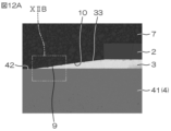
- 12A is an SEM image showing a main part of a semiconductor device according to Sample 2.
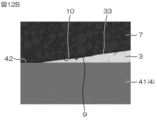
- FIG. 12B is an enlarged view of a portion surrounded by a two-dot chain line XIIB in FIG. 12A.
- FIG. 13 is an SEM image for explaining the barrier layer of the semiconductor device according to Sample 2.
- FIG. FIG. 14 is an SEM image for explaining the barrier layer of the semiconductor device according to Sample 2.
- FIG. FIG. 15 is a graph showing the relationship between the number of cycles in the temperature cycle test and the thermal resistance change rate.
- FIG. 1 is a schematic perspective view of a semiconductor device 1 according to an embodiment of the present disclosure.
- a sealing resin 7, which will be described later, is indicated by a dashed line, and the internal structure of the semiconductor device 1 is seen through.
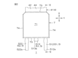
- FIG. 2 is a schematic front view of the semiconductor device 1.
- FIG. 3 is a schematic side view of the semiconductor device 1.
- FIG. 4 is a schematic rear view of the semiconductor device 1.
- FIG. 5 is a schematic bottom view of the semiconductor device 1.
- FIG. FIG. 6 is a diagram showing a cross section taken along line VI-VI of FIG.
- FIG. 7 is an enlarged view of a portion surrounded by a two-dot chain line VII in FIG.
- FIG. 8 is an enlarged view of a portion surrounded by a two-dot chain line VIII in FIG.
- the up-down direction in the plan view (FIG. 2) is defined as a first direction X
- the left-right direction in the plan view (FIG. 2) perpendicular to the first direction X is defined as a second direction Y.
- Both the first direction X and the second direction Y are perpendicular to the thickness direction (third direction Z) of the semiconductor device 1, a semiconductor element 2 described later, or the like.
- the semiconductor device 1 is, for example, of a type that is surface-mounted on a circuit board such as automotive electrical equipment.
- Semiconductor device 1 includes semiconductor element 2 , element bonding layer 3 , pad terminal 4 , lead terminal 5 , bonding wire 6 , sealing resin 7 and barrier layer 8 .
- the semiconductor element 2 is an element (semiconductor chip) that serves as the core of the functions of the semiconductor device 1 .
- the semiconductor element 2 is a power MOSFET discrete element (single-function semiconductor).
- the semiconductor element 2 is formed, for example, in a square shape with a side of 3.0 mm or more and 8.0 mm or less.
- the semiconductor element 2 has an element main surface 21 (first main surface), an element back surface 22 (second main surface), an electrode pad 23 , a passivation film 24 and a back surface electrode 25 .
- the element main surface 21 is the top surface of the semiconductor element 2 shown in FIGS. Referring to FIG. 1, electrode pads 23 are formed on element main surface 21 .
- the element back surface 22 is the bottom surface of the semiconductor element 2 shown in FIGS. 7 and 8, a rear surface electrode 25 is formed on the rear surface 22 of the element. In this embodiment, the back electrode 25 serves as the drain electrode of the semiconductor element 2 .
- the element main surface 21 and the element back surface 22 are both orthogonal to the thickness direction Z of the semiconductor element 2 and face opposite sides.
- the electrode pads 23 include first electrode pads 23a and second electrode pads 23b.
- Electrode pad 23 may be made of a metal containing Al, for example.
- the electrode pad 23 may be made of metal including, for example, Al--Cu alloy, Al--Si alloy, Al--Si--Cu alloy, or the like.
- the electrode pad 23 may be a pad having a laminated structure of Al--Cu/Ti.
- the first electrode pad 23 a is the source electrode of the semiconductor element 2 .
- the second electrode pad 23b is the gate electrode of the semiconductor element 2.
- a first electrode pad 23 a is formed in a substantially rectangular shape covering substantially the entire element main surface 21 .
- the second electrode pad 23b is formed in a recess 26 formed on one side of the first electrode pad 23a. Therefore, the area of the first electrode pad 23a is made larger than the area of the second electrode pad 23b.
- a bonding wire 6 is connected to the first electrode pad 23a and the second electrode pad 23b.
- passivation film 24 is a protective film for semiconductor element 2 formed to cover main surface 21 of the element.
- the passivation film 24 may be, for example, a laminate of a Si 3 N 4 layer formed by plasma CVD and a polyimide resin layer formed by coating. Both the first electrode pad 23 a and the second electrode pad 23 b are exposed from the passivation film 24 .
- element bonding layer 3 is a conductive member interposed between semiconductor element 2 and pad terminal 4 .
- the element bonding layer 3 allows the semiconductor element 2 to be mounted on the pad terminal 4 by die bonding, and ensures electrical connection between the semiconductor element 2 and the pad terminal 4 .
- the element bonding layer 3 is made of, for example, a solder alloy material, Ag sintered material, or the like.
- Solder alloy materials include, for example, high-temperature solder (for example, high-temperature solder having a solidus temperature of about 268°C or higher and 305°C or lower).
- the high-temperature solder may use, for example, Pb or Sn as a base material, and Ag, Sb, In, or the like may be blended in the base material.
- Pb or Sn may be used as a base material, and Ag, Sb, In, or the like may be blended in the base material.
- it may contain 85 wt % or more of Pb and 10 wt % or less of Sn, specifically Pb-5Sn, Pb-2Sn-2.5Ag.
- a SAC solder of Sn--Ag--Cu may be used as a high-temperature Pb-free solder.
- solder materials it is preferred to use a high temperature solder in this embodiment in which the semiconductor element 2 is a power MOSFET (power semiconductor). If the element bonding layer 3 is made of high-temperature solder, it can withstand relatively high heat generated from the power MOSFET. Further, when the surface-mounted semiconductor device 1 is mounted on an external circuit board, it is necessary to perform reflow processing (for example, reflow processing at about 260° C. using SAC solder) again. If the element bonding layer 3 is made of high-temperature solder, it can be prevented from melting during this reflow treatment.
- reflow processing for example, reflow processing at about 260° C. using SAC solder
- the pad terminal 4 is a conductive member that forms a conductive path between the semiconductor device 1 and the circuit board by being joined to the circuit board.
- Pad terminals 4 include die pads 41 in this embodiment. In the following description, the pad terminals 4 are assumed to be the die pads 41 unless otherwise required.
- the die pad 41 is made of an alloy containing Cu.
- the die pad 41 has a thickness of, for example, 1.0 mm or more and 2.0 mm or less. If the die pad 41 has a thickness of 1.0 mm or more and 2.0 mm or less, the thermal resistance of the die pad 41 can be made relatively low. Thereby, the heat dissipation of the semiconductor device 1 can be improved.
- die pad 41 is a portion on which semiconductor element 2 is mounted.
- Die pad 41 has mounting surface 42 and mounting surface 43 .
- the mounting surface 42 is the surface on which the semiconductor element 2 is mounted, and the mounting surface 43 is the surface facing away from the mounting surface 42 .
- the mounting surface 42 is the top surface of the die pad 41 shown in FIGS.
- the mounting surface 43 is the lower surface of the die pad 41 shown in FIGS. 6-8. Both the mounting surface 42 and the mounting surface 43 are flat. Both the mounting surface 42 and the mounting surface 43 may be covered with an exterior plating layer.
- the exterior plating layer provides good solder adhesion to the portions of the pad terminals 4 exposed from the sealing resin 7 when the semiconductor device 1 is surface-mounted on the circuit board by soldering by reflow, and soldering is performed. It functions to prevent erosion of the portion due to bonding.
- the element bonding layer 3 is interposed between the element back surface 22 (back surface electrode 25) and the mounting surface 42, and the die pad 41 is connected to the back surface electrode 25 via the element bonding layer 3.
- the die pad 41 (pad terminal 4 ) functions as a drain terminal of the semiconductor device 1 .
- both the mounting surface 42 and the mounting surface 43 are partially exposed from the sealing resin 7 .
- a portion of the die pad 41 that protrudes from the end surface of the sealing resin 7 (resin first side surface 73 described later) may be referred to as a protruding portion 44 of the die pad 41 .
- the element bonding layer 3 includes a body portion 31 sandwiched between the die pad 41 and the semiconductor element 2 and a peripheral portion formed around the semiconductor element 2. 32 integrally.
- the body portion 31 forms a main path of a conductive path and a heat dissipation path between the die pad 41 and the back electrode 25 in the element bonding layer 3 .
- the peripheral portion 32 may be a surplus portion of solder material protruding outside the semiconductor element 2 when the semiconductor element 2 is mounted on the die pad 41 by reflow soldering.
- the peripheral portion 32 surrounds the semiconductor element 2 .
- the peripheral portion 32 forms a sub-path of the conductive path and the heat dissipation path.
- the element bonding layer 3 may be composed only of the body part 31 without the peripheral part 32 , or part of the peripheral part 32 may be wetted to the end surface of the semiconductor element 2 .
- peripheral portion 32 of element bonding layer 3 has an inclined surface 33 inclined with respect to mounting surface 42 of die pad 41 .
- the inclined surface 33 is inclined downward from the vicinity of the lower edge corner portion 27 of the semiconductor element 2 toward the mounting surface 42 .
- the inclined surface 33 is flat and inclined at an angle ⁇ 1 of, for example, 5° or more and 45° or less with respect to the mounting surface 42 .
- the peripheral portion 32 may have a curved side surface 34 reaching the mounting surface 42 from the vicinity of the lower edge corner portion 27 of the semiconductor chip 2 instead of the flat inclined surface 33 .
- the peripheral portion 32 may have a length L of 0.1 mm or more and 2 mm or less with respect to the thickness T of the element bonding layer 3 (for example, 50 ⁇ m or more and 200 ⁇ m or less).
- the lead terminal 5 is a conductive member that forms a conductive path between the semiconductor device 1 and the circuit board by being joined to the circuit board. Referring to FIG. 1 , lead terminal 5 is arranged adjacent to pad terminal 4 in first direction X and electrically connected to electrode pad 23 . 1, 2, 4 and 5, lead terminal 5 includes a first lead terminal 51 and a second lead terminal 52 adjacent to each other in second direction Y in plan view. In this embodiment, the lead terminals 5 are made of an alloy containing Cu, like the pad terminals 4 . Moreover, in this embodiment, the lead terminal 5 has a thickness of, for example, 1.0 mm or more and 2.0 mm or less.
- a bonding wire 6 is connected to the first lead terminal 51 .
- the first lead terminal 51 is electrically connected through the bonding wire 6 to the first electrode pad 23a. Therefore, the first lead terminal 51 is the source terminal of the semiconductor device 1 .
- the first lead terminal 51 has a first pad portion 511 , a first lead portion 512 and a dummy lead portion 513 .
- the first pad portion 511 is a substantially quadrangular portion in plan view to which the bonding wire 6 is connected.
- the first pad portion 511 is flat and entirely covered with the sealing resin 7 .
- the first lead portion 512 is a substantially rectangular portion connected to the first pad portion 511 and arranged parallel to the first direction X in a plan view.
- the first lead portion 512 has a portion exposed from the sealing resin 7 . 1, 3 and 6, the exposed portion of first lead portion 512 is bent into a gull-wing shape.
- a tip portion 512a of the first lead portion 512 is a portion of the first lead terminal 51 that is joined to the circuit board. Referring to FIG.
- the dummy lead portion 513 is a substantially rectangular portion connected to the first pad portion 511 and arranged parallel to the first direction X in plan view.
- the dummy lead portion 513 extends parallel to the first lead portion 512 in the first direction X from the first pad portion 511 . Therefore, the first lead portion 512 and the dummy lead portion 513 are adjacent to each other in the second direction Y.
- Dummy lead portion 513 has a portion exposed from sealing resin 7 .
- the exposed portion of the dummy lead portion 513 is flat. Therefore, the distal end portion 513 a of the dummy lead portion 513 is located above the distal end portion 512 a of the first lead portion 512 in the third direction Z.
- the dummy lead portions 513 are not in contact with the circuit board and are cantilevered by the sealing resin 7 .
- the bonding wire 6 is connected to the second lead terminal 52 .
- the second lead terminal 52 is electrically connected through the bonding wire 6 to the second electrode pad 23b. Therefore, the second lead terminal 52 is the gate terminal of the semiconductor device 1 .
- the second lead terminal 52 has a second pad portion 521 and a second lead portion 522 .
- the second pad portion 521 is a portion having a substantially square shape in plan view to which the bonding wire 6 is connected.
- the second pad portion 521 is flat and entirely covered with the sealing resin 7 .
- the second lead portion 522 is a substantially quadrangular portion connected to the second pad portion 521 and arranged parallel to the first direction X in plan view.
- the second lead portion 522 has a portion exposed from the sealing resin 7 .
- the exposed portion of second lead portion 522 is bent into a gull-wing shape.
- the shape of the second lead portion 522 is the same as the shape of the first lead portion 512 .
- a distal end portion 522a of the second lead portion 522 is a portion of the second lead terminal 52 that is joined to the circuit board.
- the bonding wires 6 include first bonding wires 61 and second bonding wires 62 .
- first bonding wire 61 is a conductive member that connects first electrode pad 23 a and first pad portion 511 of first lead terminal 51 . Therefore, first bonding wire 61 is the source wire of semiconductor device 1 .
- the first bonding wire 61 is made of Al or an Al alloy, for example.
- the first bonding wire 61 has a diameter of, for example, 250 ⁇ m or more and 500 ⁇ m or less.
- the second bonding wire 62 is a conductive member that connects the second electrode pad 23 b and the second pad portion 521 of the second lead terminal 52 .
- the second bonding wire 62 is the gate wire of the semiconductor device 1 .
- the second bonding wire 62 is made of Al or an Al alloy, for example.
- the second bonding wire 62 is thinner than the first bonding wire 61 and has a diameter of 100 ⁇ m or more and 200 ⁇ m or less, for example.
- the sealing resin 7 is made of black resin having electrical insulation.
- the sealing resin 7 includes, for example, a thermosetting resin such as an epoxy resin as a matrix resin (base resin), a filler, a silane coupling agent as an additive, a curing agent, a curing accelerator, and the like.
- fillers include silica filler, talc, clay, glass beads, glass fiber and the like.
- the silane coupling agent has, for example, a function of improving adhesion between the organic surface of the sealing resin 7 and the inorganic surface such as glass or metal.
- Examples of curing agents include amine-based curing agents, acid anhydride-based curing agents, phenol resins, amino resins, and the like.
- curing accelerators include phosphorus-based curing accelerators, tertiary amine-based curing accelerators, and imidazole-based curing accelerators. In this embodiment, a phosphorus accelerator is used.
- the sealing resin 7 partially covers the pad terminals 4 and the lead terminals 5 as well as the semiconductor element 2 and the bonding wires 6 .
- the sealing resin 7 is formed by transfer molding using a mold.
- the sealing resin 7 has a resin main surface 71 , a resin back surface 72 , a resin first side surface 73 , a resin second side surface 74 and a resin inner surface 75 .
- the resin main surface 71 is the top surface of the sealing resin 7 shown in FIGS.
- the resin back surface 72 is the bottom surface of the sealing resin 7 shown in FIGS.
- the resin main surface 71 and the resin back surface 72 are both orthogonal to the thickness direction Z of the semiconductor device 1 and face opposite sides. In this embodiment, the mounting surface 43 is exposed from the resin back surface 72 .
- the first resin side surfaces 73 are a pair of surfaces that are spaced apart in the first direction X.
- the pair of resin first side surfaces 73 face opposite sides.
- the upper end of the resin first side surface 73 is connected to the resin main surface 71
- the lower end of the resin first side surface 73 is connected to the resin back surface 72 .
- a part of each of the first lead terminal 51 and the second lead terminal 52 is exposed from one resin first side surface 73 . 2 to 4, the projecting portion 44 of the die pad 41 is exposed from the resin first side surface 73 on the other side.
- the resin second side surfaces 74 are a pair of surfaces spaced apart in the second direction Y.
- the pair of resin second side surfaces 74 face opposite sides.
- the upper end of the resin second side surface 74 is connected to the resin main surface 71
- the lower end of the resin second side surface 74 is connected to the resin back surface 72 .
- the pad terminal 4 or the lead terminal 5 is not exposed from the resin second side surface 74 .
- the resin inner surface 75 is either a surface where the sealing resin 7 contacts the internal structure covered with the sealing resin 7 or a surface facing the internal structure through a space such as a gap 9 to be described later.
- the surface in contact with the internal structure broadly includes the case where a space such as a gap is not formed between the internal structure, the surface in direct contact with the internal structure, and the intermediate layer such as the barrier layer 8. may also include surfaces that are in indirect contact with each other.
- the resin inner surface 75 is a first inner surface 751 which is a contact surface between the sealing resin 7 and the semiconductor element 2, and a contact surface between the sealing resin 7 and the element bonding layer 3.
- a second inner surface 752 a third inner surface 753 that is a contact surface between the sealing resin 7 and the pad terminal 4 (die pad 41 ), and a fourth inner surface 754 that is a contact surface between the sealing resin 7 and the lead terminal 5 .
- a fifth inner surface 755 that is a contact surface between the sealing resin 7 and the bonding wire 6 .
- gap 9 extending from the end surface of sealing resin 7 (in this embodiment, first resin side surface 73 having projecting portion 44 formed thereon) toward semiconductor element 2 is provided.
- the gap 9 extends upward along the mounting surface 42 of the die pad 41 and the inclined surface 33 of the element bonding layer 3 from the resin first side surface 73 of the sealing resin 7 in a cross-sectional view.
- the tip portion 91 corresponds to the dead end of the gap 9 when the resin first side surface 73 of the sealing resin 7 is used as the entrance of the gap 9 .
- the resin inner surface 75 facing the die pad 41 and the element bonding layer 3 through the gap 9 may be the sixth inner surface 756 .
- the sixth inner surface 756 is separated from the die pad 41 and the element bonding layer 3 across the gap 9 . Therefore, on the inclined surface 33 of the element bonding layer 3 , the area from the lower edge corner 27 of the semiconductor element 2 to the middle of the inclined surface 33 is the second inner surface 752 . 42 is the sixth inner surface 756 .
- the surfaces (first to fifth inner surfaces 751 to 755 in this embodiment) in contact with the internal structure such as the semiconductor element 2 and the die pad 41 in the sealing resin 7 are collectively referred to as It may be defined as an internal resin contact surface, and a surface separated from the internal structure via a space such as the gap 9 (the sixth internal surface 756 in this embodiment) may be generically defined as an internal resin separation surface.
- the barrier layer 8 is made of a material having a function of blocking corrosive ions derived from the sealing resin 7 from contacting the element bonding layer 3 .
- the corrosive ions are ions that can attack and corrode the device bonding layer 3 .
- ions that are inherently contained in the sealing resin 7 and ions that are generated due to chemical changes or alterations in the constituent substances of the sealing resin 7 can be used.
- SiO 3 H ions derived from silane coupling agents, PO 3 ions derived from phosphorus curing accelerators, COOH ions generated by oxidation of epoxy resins, and the like can be mentioned.
- constituent substances of the element bonding layer 3 are easily ionized (for example, Pb is ionized into Pb ions), the element bonding layer 3 is electrochemically corroded, and voids are formed in the element bonding layer 3. or cracks may occur.
- the barrier layer 8 that prevent such voids and cracks include aluminum oxide (Al 2 O 3 ), silicon oxide (SiO 2 ), zirconium oxide (ZrO 2 ), tantalum pentoxide (Ta 2 O 5 ), hafnium dioxide (HfO 2 ), yttrium oxide (Y 2 O 3 ) and multilayer structures thereof.
- Al 2 O 3 is used in this embodiment.
- the barrier layer 8 may have a thickness of 50 nm or more and 10 ⁇ m or less.
- barrier layer 8 protects the internal structure of semiconductor element 2, element bonding layer 3, pad terminal 4 (die pad 41), lead terminal 5, bonding wire 6, etc. in sealing resin 7. It is formed so as to cover the whole. 6 to 8 of the semiconductor element 2, the pad terminal 4 (die pad 41), the element bonding layer 3, and the lead terminal 5 inside the sealing resin 7 are covered with the barrier layer 8. .
- the barrier layer 8 does not cover the protruding portion 44 of the die pad 41 and the exposed portions of the lead terminals 5 outside the sealing resin 7 .
- a conductive terminal surface for ensuring conduction with the circuit board is ensured in the pad terminal 4 (die pad 41) and the lead terminal 5 in the outer portion of the sealing resin 7. As shown in FIG.
- barrier layer 8 forms boundary portion 10 between element bonding layer 3 (peripheral portion 32 ) and sealing resin 7 .
- a part of the barrier layer 8 is held in close contact with the resin inner surface 75 of the sealing resin 7 while floating from the die pad 41 via the gap 9 .
- the barrier layer 8 seals between the separation portion 81 floating from the die pad 41 and the element bonding layer 3 through the gap 9 and between the lower edge corner portion 27 of the semiconductor element 2 and the tip portion 91 of the gap 9 .
- a sandwiching portion 82 sandwiched between the sealing resin 7 and the element bonding layer 3 may be included.
- FIG. 9 is a flowchart showing an example of the manufacturing process of the semiconductor device 1. As shown in FIG.
- the method of manufacturing semiconductor device 1 mainly includes component preparation step S1, die bonding step S2, wire bonding step S3, barrier layer forming step S4, resin sealing step S5 and final step S6. You can stay.
- the method for manufacturing the semiconductor device 1 may include steps not shown in FIG.
- the component preparation step S1 is a step of preparing each component of the semiconductor device 1 described above. For example, from a wafer of semiconductor elements 2, semiconductor elements 2 of a predetermined size are produced by dicing the wafer. Also, a lead frame in which the pad terminal 4 (die pad 41) and the lead terminal 5 are integrally connected is molded by molding.
- the die-bonding step S2 is a step of die-bonding the semiconductor element 2 .
- the die bonding step S2 is performed using, for example, a well-known die bonder, and may be called a mounting step.
- the die bonding step S2 is a step of conductively bonding the semiconductor element 2 to the die pad 41 by the element bonding layer 3 .
- a paste bonding material for example, solder paste, Ag paste, etc.
- the atmosphere temperature in the furnace is raised to the melting point of the bonding material (for example, 300° C. or more and 390° C.
- the ambient temperature in the furnace is lowered to normal temperature (below the melting point of the bonding material), and the bonding material is cured to form the element bonding layer 3 .
- the semiconductor element 2 and the die pad 41 are electrically connected.
- the wire bonding step S3 is a step of bonding the first bonding wire 61 and the second bonding wire 62.
- the wire bonding step S3 is performed using, for example, a known wire bonder.
- the wire bonding step S3 uses the wire bonder to perform wire bonding between one end of the first bonding wire 61 and the first electrode pad 23a and wire bonding between the other end of the first bonding wire 61 and the first pad portion 511. including the step of performing Specifically, first, the tip of the wire is protruded from the capillary of the wire bonder and melted to form the tip of the wire into a ball shape. Then, the tip portion is pressed against the first electrode pad 23a.
- the wire bonding step S3 uses the wire bonder to perform wire bonding between one end of the second bonding wire 62 and the second electrode pad 23b, and wire bonding of the other end of the second bonding wire 62 and the second pad portion. 521 is included.
- all wire joints may be wedge bonds.
- a wedge bond is formed by pressing a wire into place and cutting the wire.
- each wire bonding portion may be distinguished from the first bonding and the second bonding according to the order in which the wires are bonded.
- the first electrode pad 23a and the second electrode pad 23b are first-bonded, and the first pad portion 511 and the second pad portion 521 are second-bonded.
- the first bonding may be performed on the first pad portion 511 and the second pad portion 521, and the second bonding may be performed on the first electrode pad 23a and the second electrode pad 23b.
- the barrier layer forming step S4 is a step of covering the semiconductor element 2, the element bonding layer 3, the pad terminal 4 (die pad 41), the lead terminal 5 and the bonding wire 6 with the barrier layer 8.
- FIG. The barrier layer forming step S4 is performed by, for example, a well-known film forming method.
- an Al 2 O 3 film is formed by an ion plating method, a sputtering method, or the like.
- the film forming temperature of the barrier layer 8 may be, for example, room temperature or higher and 300° C. or lower.
- the resin sealing step S5 is a step of forming the sealing resin 7 and packaging the semiconductor device 1 . That is, the resin sealing step S5 is a step of forming the sealing resin 7 having the shape described above.
- the resin sealing step S5 is performed, for example, by well-known transfer molding using a mold. Specifically, after the barrier layer 8 is formed, the lead frame to which the semiconductor element 2 is bonded is set in a mold molding machine, and the fluidized epoxy resin is poured into the mold for molding. Then, the epoxy resin is cured, and the molded lead frame is taken out. Then, it is shaped into the shape of the above-described sealing resin 7 by removing excess resin, burrs, or the like.
- the final step S6 is a step of forming the semiconductor device 1 into the shape shown in FIG. 1 and finishing the semiconductor device 1 into a product that can be shipped.
- the final step S6 includes, for example, a step of removing burrs from the sealing resin 7, a cutting step of cutting unnecessary portions of the lead frame exposed to the outside of the sealing resin 7, and a step of bending the lead frame exposed to the outside of the sealing resin 7.
- An exterior treatment process for improving strength, improving solder wettability at the time of mounting on a circuit board or the like, preventing rust, etc., a cleaning process before the exterior treatment process, and removing the lead frame exposed to the outside of the sealing resin 7 in a predetermined manner.
- a lead processing process that bends the product into a shape, a stamping process that stamps the company name, product name, lot number, etc. on the package, and an inspection and sorting process that determines whether the product is good or not is performed. Note that these steps may be appropriately performed according to the final specifications of the semiconductor device 1 .
- the barrier layer 8 formed on the lead terminals 5 exposed to the outside of the sealing resin 7 is removed, and the exterior surfaces of the lead terminals 5 are exposed.
- the semiconductor device 1 shown in FIG. 1 is completed. [Verification of generation of corrosive ions] FIG.
- FIG. 10 is a diagram for verifying that corrosive ions are generated at the boundary 10 between the sealing resin 7 and the element bonding layer 3.
- FIG. 10 shows an optical microscope image of the boundary 10 between the sealing resin 7 and the element bonding layer 3 in the sample 1, and time-of-flight secondary ion mass spectrometry (TOF-SIMS). ) is a graphical representation of the analysis result image.
- the sealing resin 7 is an epoxy resin containing at least a silane coupling agent and a phosphorus-based curing accelerator as additives and a silica filler as filler 11 .
- the element bonding layer 3 is a high temperature solder made of Pb-2Sn-2.5Ag.
- the leftmost mass corresponds to the optical microscope image
- the other masses are the results of TOF-SIMS analysis of Si ions, Pb ions, SiO 3 H ions, PO 3 ions and COOH ions.
- Each detected fragment containing The diagrams of the detected fragments all show the analysis results of the boundary portion 10 in the same way as the optical microscope image, but for the sake of clarity, the reference numerals of the sealing resin 7 and the element bonding layer 3 are omitted. ing.
- each figure in the upper row shows the state after assembly (immediately after manufacture) of the semiconductor device of Sample 1 and before the temperature cycle test (TC) is performed.
- the lower figures show the state after the temperature cycle test (TC) was performed on the semiconductor device of Sample 1.
- FIG. In the temperature cycle test, the semiconductor device after assembly is exposed to an environment of MSL1 (Moisture Sensitivity Level 1) in accordance with IPC/JEDEC J-STD-020. It was carried out by repeating 1000 cycles of heating and cooling between.
- MSL1 Microisture Sensitivity Level 1
- the element bonding layer 3 was corroded, and that the gap 14 and the crack 12 were generated on the element bonding layer 3 side with respect to the boundary portion 10 .
- the causes of the voids 14 and the cracks 12 are the thermal stress (tensile stress) generated in the boundary portion 10 during the temperature cycle test, and the corrosive ions (corrosive stress) in the boundary portion 10 . chemical species) are generated, and it was found that the corrosive action by the corrosive ions is related.
- SiO 3 H ions, PO 3 ions and COOH ions are widely distributed in the regions where voids 14 and cracks 12 are generated, thereby ionizing Pb in the high-temperature solder and causing corrosion to progress.
- SiO 3 H ions are the source of the silane coupling agent in the sealing resin 7
- PO 3 ions are the source of the phosphorus-based curing accelerator in the sealing resin 7
- COOH ions are the source of the sealing resin 7 .
- the epoxy resin of is produced by oxidation.
- the generation of corrosive ions in the boundary portion 10 under the conditions that the voids 14 and the cracks 12 are likely to occur due to the thermal stress during the temperature cycle test causes the alloy of the element bonding layer 3 (solder alloy) to It is considered that the compositional balance of is disturbed, and the generation of voids 14 and cracks 12 is accelerated.
- FIG. 11A is an SEM image showing a main part of the semiconductor device according to Sample 1.
- FIG. 11B is an SEM image showing a main part of the semiconductor device according to Sample 1.
- FIG. 11B is an enlarged view of a portion surrounded by a two-dot chain line XIB in FIG. 11A.
- 12A is an SEM image showing a main part of a semiconductor device according to Sample 2.
- FIG. 12B is an enlarged view of a portion surrounded by a two-dot chain line XIIB in FIG. 12A.
- FIG. 13 is an SEM image for explaining the barrier layer 8 of the semiconductor device according to Sample 2.
- FIG. FIG. 14 is an SEM image for explaining the barrier layer 8 of the semiconductor device according to Sample 2.
- FIG. FIG. 15 is a graph showing the relationship between the number of cycles in the temperature cycle test and the thermal resistance change rate.
- Sample 2 which is to be compared with Sample 1, has a barrier layer 8 (Al 2 O 3 layer) between the sealing resin 7, the die pad 41 (pad terminal 4) and the element bonding layer 3, except that: It has the same structure as sample 1. As shown in FIG. 13, in sample 2, barrier layer 8 sandwiched between sealing resin 7 and element bonding layer 3 can be confirmed. That is, the overall structure of Sample 2 is the same as the structure shown in FIGS. 1-8.
- FIGS. 11A and 11B are SEM images after 750 cycles of the temperature cycle test described above.
- FIGS. 11A and 11B since the barrier layer 8 is not formed in the sample 1, a large gap 14 is formed in the boundary portion 10 between the sealing resin 7 and the element bonding layer 3, and the element bonding is performed from the gap 14. Cracks 12 extending into the interior of layer 3 were confirmed. The gaps 14 and the cracks 12 are distributed over the entire inclined surface 33 of the element bonding layer 3 , and the cracks 12 form the conductive paths and the heat dissipation paths between the semiconductor element 2 and the element bonding layer 3 immediately below the semiconductor element 2 .
- FIGS. 12A and 12B no conspicuous voids 14 or cracks 12 were observed even after 750 cycles of the temperature cycle test.
- a gap 9 is formed between the sealing resin 7 and the element bonding layer 3 due to interfacial peeling, but the peeling stops halfway along the inclined surface 33 of the element bonding layer 3 .
- the barrier layer 8 was held in close contact with the internal resin surface of the sealing resin 7 while floating from the die pad 41 in the gap 9 (see also FIG. 8). See also).
- the sealing resin 7 of sample 2 did not show discoloration like that seen in sample 1 even after the temperature cycle test.
- the barrier layer 8 is formed between the sealing resin 7 and the element bonding layer 3, contact between the corrosive ions and the element bonding layer 3 is suppressed. can be prevented. Accordingly, corrosion of the element bonding layer 3 can be suppressed, and weakening of the strength of the element bonding layer 3 can be suppressed. As a result, cracks in the element bonding layer 3 can be suppressed even if stress is applied to the element bonding layer 3 , so that deterioration of heat dissipation through the element bonding layer 3 can be suppressed.
- the electrical resistance is as low as possible.
- various members for example, pad terminals 4, lead terminals 5, bonding wires 6, etc.
- the barrier layer 8 can suppress the corrosion of the element bonding layer 3 , and can suppress the weakening of the strength of the element bonding layer 3 . Therefore, even if a large stress is applied to the element bonding layer 3, it is possible to suppress the occurrence of cracks over a wide area.
- the semiconductor device 1 is surface-mounted on a circuit board or the like via a pad terminal 4 (die pad 41) that is a drain terminal.
- the surface mount type semiconductor device 1 is mounted by reflowing a bonding material for attachment to a circuit board (for example, paste for attachment such as Pb-free solder). Thermal stress is more likely to be applied to the element bonding layer 3 from the attachment bonding material via the die pad 41 in the surface-mounted semiconductor device 1 than in the flow-mounted semiconductor device having pin terminals.
- the barrier layer 8 can prevent the strength of the element bonding layer 3 from weakening, as described above. Therefore, it is possible to suppress the occurrence of cracks due to the thermal stress applied to the element bonding layer 3, so that it is possible to provide a power semiconductor having high heat dissipation reliability.
- a gap 9 is formed at the base end of the protruding portion 44 so as to extend from the first resin side surface 73 of the sealing resin 7 to the inside of the sealing resin 7 . That is, the space 9 is formed between the resin inner surface 75 of the sealing resin 7 and the die pad 41 , and the environment is such that oxygen and moisture easily enter the inside of the sealing resin 7 . Therefore, oxygen enters between the sealing resin 7 and the element bonding layer 3, and an environment may be created in which a part of the sealing resin 7 (epoxy resin) is oxidized to generate corrosive ions. However, the barrier layer 8 is in close contact with the resin inner surface 75 of the sealing resin 7 . As a result, even if oxygen or moisture enters the gap 9, contact between the sealing resin 7 and oxygen or moisture can be effectively prevented, and generation of corrosive ions derived from the sealing resin 7 can be suppressed. .
- this type of crack is formed by a crack 12 extending in the lateral direction directly under the semiconductor element 2 so as to divide the conductive path and the heat radiation path between the semiconductor element 2 and the element bonding layer 3. Applicable.
- the gap 9 extending from the resin first side surface 73 of the sealing resin 7 does not reach the lower edge corner portion 27 of the semiconductor element 2 .
- FIG. 15 is a graph showing the relationship between the number of cycles in the temperature cycle test and the rate of change in thermal resistance for samples 1 and 2. As shown in FIG. With reference to FIG. 15, it will be verified to what extent the formation of the barrier layer 8 suppresses heat dissipation.
- FIG. 15 shows the rate of thermal resistance change at 300, 500, 750 and 1000 cycles with respect to the thermal resistance (0%) of the semiconductor device before the temperature cycle test for Samples 1 and 2 described above. ing.
- the rate of change in thermal resistance of the semiconductor device starts to increase after about 200 cycles, and increases sharply after about 500 cycles.
- the thermal resistance change rate increases after 500 cycles, but the thermal resistance change rate at 1000 cycles is about 10%, which is about 30% for sample 1.
- a much lower thermal resistivity could be maintained. From this verification result, it can be seen that the formation of the barrier layer 8 can suppress the occurrence of cracks in the element bonding layer 3 and suppress the deterioration of heat dissipation.
- the barrier layer (8) is formed between the sealing resin (7) and the element bonding layer (3), contact between corrosive ions and the element bonding layer (3) is prevented. can do. Thereby, corrosion of the element bonding layer (3) can be suppressed, and weakening of the strength of the element bonding layer (3) can be suppressed. As a result, even if stress is applied to the element bonding layer (3), cracks (12) can be prevented from occurring in the element bonding layer (3). be able to.
- the sealing resin (7) has end surfaces (73, 74) forming the peripheral contour of the sealing resin (7), According to Appendix 1-1, the die pad (41) includes a projecting portion (44) projecting outward from the sealing resin (7) starting from the end surfaces (73, 74) of the sealing resin (7)
- the sealing resin (7) has an inner surface (75) facing the semiconductor element (2), the element bonding layer (3) and the die pad (41), At least between the inner surface (75) of the sealing resin (7) and the die pad (41), there extends from end surfaces (73, 74) of the sealing resin (7) toward the semiconductor element (2) A gap (9) is formed, A part of the barrier layer (8) is held in close contact with the inner surface (75) of the sealing resin (7) while floating from the die pad (41) through the gap (9).
- the semiconductor device (1) according to Appendix 1-2, wherein:
- the gap (9) is formed between the inner surface (75) of the sealing resin (7) and the die pad (41), and oxygen and moisture are prevented from entering the sealing resin (7).
- the barrier layer (8) is in intimate contact with the inner surface (75) of the encapsulating resin (7), although it is an intrusive environment. As a result, even if oxygen or moisture enters the gap (9), contact between the sealing resin (7) and oxygen or moisture is effectively prevented, and corrosive ions derived from the sealing resin (7) are generated. can be suppressed.
- the gap (9) extends from the end surfaces (73, 74) of the sealing resin (7) along the die pad (41) and the element bonding layer (3), and extends on the element bonding layer (3). having an end (91),
- the barrier layer (8) includes a separation portion (81) floating from the die pad (41) and the element bonding layer (3) through the gap (9), and a lower edge of the semiconductor element (2). a holding portion (82) sandwiched between the sealing resin (7) and the element bonding layer (3) between the corner (27) and the end (91) of the gap (9);
- the semiconductor device (1) according to appendix 1-3, comprising:
- the crack (12) when a crack (12) occurs in the element bonding layer (3) in a region inside the semiconductor element (2) from the lower edge corner (27) of the semiconductor element (2), the crack (12) is It can be a heat dissipation resistor that transfers heat from (2) to the die pad (41) immediately below.
- the gap (9) extending from the end surfaces (73, 74) of the sealing resin (7) does not reach the lower edge corner (27) of the semiconductor element (2). Therefore, for example, even if corrosive ions originating from the outside enter the gap (9), a crack (12) occurs in the element bonding layer (3) at least in the vicinity of the lower edge corner (27) of the semiconductor element (2). can be prevented. As a result, it is possible to suppress deterioration in heat dissipation through the element bonding layer (3).
- the element bonding layer (3) is in close contact with the sealing resin (7) via the barrier layer (8) (sandwiching portion (82)), the stress applied to the element bonding layer (3) is reduced. be able to.
- the close contact between the sealing resin (7) and the element bonding layer (3) via the barrier layer (8) can also prevent cracks (12) from occurring in the element bonding layer (3).
- the element bonding layer (3) includes a body portion (31) sandwiched between the die pad (41) and the semiconductor element (2) and a peripheral portion (31) formed around the semiconductor element (2). 32), integrally including a peripheral portion (32) having an inclined surface (33) inclined with respect to the die pad (41), The gap (9) is formed so as to warp upward along the surface (42) of the die pad (41) and the inclined surface (33) of the element bonding layer (3) in a cross-sectional view.
- the semiconductor device (1) according to 1-4.
- the semiconductor element (2) has a first main surface (21) and an element rear surface (22) on the opposite side, and a gate electrode (23b) and a source electrode (23a) are provided on the first main surface (21). and a power semiconductor in which a drain electrode (25) electrically connected to the die pad (41) through the element bonding layer (3) is formed on the element back surface (22). 1.
- the semiconductor device (1) according to any one of Appendices 1-6.
- a temperature cycle test is one of the various reliability tests for semiconductor devices (1). Since a power semiconductor needs to pass a large current, it is preferable that the resistance value is as low as possible. In order to reduce the resistance, for example, various members (for example, external terminals, internal wires, etc.) that constitute the semiconductor device (1) tend to be large, and as a result, the transfer from these members to the element bonding layer (3) stress tends to increase. Therefore, cracks (12) are likely to occur in the element bonding layer (3) due to the stress. On the other hand, according to this configuration, the barrier layer (8) can suppress corrosion of the element bonding layer (3), and can suppress weakening of the element bonding layer (3). Therefore, even if a large stress is applied to the element bonding layer (3), cracks (12) can be prevented from occurring over a wide area.
- various members for example, external terminals, internal wires, etc.
- the die pad (41) is exposed from the sealing resin (7) as a drain terminal (4) on a mounting surface (42) on which the semiconductor element (2) is mounted and on the side opposite to the mounting surface (42). a mounting surface (43); a source lead terminal (51) electrically connected to the source electrode (23a) in the sealing resin (7) and exposed from the sealing resin (7); and a gate lead terminal (52) electrically connected to the gate electrode (23b) within the sealing resin (7) and exposed from the sealing resin (7).
- a semiconductor device (1) is exposed from the sealing resin (7) as a drain terminal (4) on a mounting surface (42) on which the semiconductor element (2) is mounted and on the side opposite to the mounting surface (42). a mounting surface (43); a source lead terminal (51) electrically connected to the source electrode (23a) in the sealing resin (7) and exposed from the sealing resin (7); and a gate lead terminal (52) electrically connected to the gate electrode (23b) within the sealing resin (7) and exposed from the sealing resin (7).
- the semiconductor device (1) can be surface-mounted on a circuit board or the like through the die pad (41) which is the drain terminal (4).
- a surface mount type semiconductor device (1) is mounted by reflowing a bonding material for attachment (for example, paste for attachment) to a circuit board.
- stress is applied to the element bonding layer (3) from the attachment bonding material through the die pad (41), compared to the semiconductor device having pin terminals mounted by the flow method.
- the barrier layer (8) can suppress the occurrence of cracks (12) due to the stress applied to the element bonding layer (3).
- a semiconductor can be provided.
- the die pad (41) has a thickness of 1.0 mm or more and 2.0 mm or less, so the thermal resistance of the die pad (41) can be relatively low. Thereby, the heat dissipation of the semiconductor device (1) can be improved.
- Appendix 1-12 The semiconductor device (1) according to any one of Appendixes 1-1 to 1-11, wherein the device bonding layer (3) includes a device bonding layer (3) containing a solder alloy.
- the barrier layer (8) can block the contact between the corrosive ions and the element bonding layer (3), so that it is possible to suppress the breakdown of the compositional balance of the alloy. As a result, it is possible to prevent the element bonding layer (3) from weakening in terms of strength.
- thermosetting base resin comprises an epoxy resin
- Appendix 1-16 The semiconductor device according to any one of Appendixes 1-1 to 1-15, wherein the element bonding layer (3) has a thickness of 50 ⁇ m or more and 200 ⁇ m or less.
- Appendix 1-17 The semiconductor device according to any one of Appendixes 1-1 to 1-16, wherein the barrier layer (8) has a thickness of 50 nm or more and 10 ⁇ m or less.
- Reference Signs List 1 Semiconductor device 2 : Semiconductor element 3 : Element bonding layer 4 : Pad terminal 5 : Lead terminal 6 : Bonding wire 7 : Sealing resin 8 : Barrier layer 9 : Gap 10 : Boundary 11 : Filler 12 : Crack 13 : Distribution area 14 : Gap 21 : Element main surface 22 : Element back surface 23 : Electrode pad 23a : First electrode pad 23b : Second electrode pad 24 : Passivation film 25 : Back surface electrode 26 : Concave portion 27 : Lower edge corner 31 : Main body Part 32 : Peripheral part 33 : Inclined surface 34 : Side surface 41 : Die pad 42 : Mounting surface 43 : Mounting surface 44 : Projecting portion 51 : First lead terminal 52 : Second lead terminal 61 : First bonding wire 62 : Second bonding Wire 71 : Resin main surface 72 : Resin back surface 73 : Resin first side surface 74 : Resin second side
Landscapes
- Structures Or Materials For Encapsulating Or Coating Semiconductor Devices Or Solid State Devices (AREA)
Priority Applications (4)
| Application Number | Priority Date | Filing Date | Title |
|---|---|---|---|
| CN202280058306.5A CN117897807A (zh) | 2021-10-13 | 2022-09-26 | 半导体装置 |
| JP2023555075A JPWO2023063064A1 (https=) | 2021-10-13 | 2022-09-26 | |
| DE112022004390.3T DE112022004390T5 (de) | 2021-10-13 | 2022-09-26 | Halbleiterbauelement |
| US18/414,969 US20240153836A1 (en) | 2021-10-13 | 2024-01-17 | Semiconductor device |
Applications Claiming Priority (2)
| Application Number | Priority Date | Filing Date | Title |
|---|---|---|---|
| JP2021168410 | 2021-10-13 | ||
| JP2021-168410 | 2021-10-13 |
Related Child Applications (1)
| Application Number | Title | Priority Date | Filing Date |
|---|---|---|---|
| US18/414,969 Continuation US20240153836A1 (en) | 2021-10-13 | 2024-01-17 | Semiconductor device |
Publications (1)
| Publication Number | Publication Date |
|---|---|
| WO2023063064A1 true WO2023063064A1 (ja) | 2023-04-20 |
Family
ID=85988495
Family Applications (1)
| Application Number | Title | Priority Date | Filing Date |
|---|---|---|---|
| PCT/JP2022/035719 Ceased WO2023063064A1 (ja) | 2021-10-13 | 2022-09-26 | 半導体装置 |
Country Status (5)
| Country | Link |
|---|---|
| US (1) | US20240153836A1 (https=) |
| JP (1) | JPWO2023063064A1 (https=) |
| CN (1) | CN117897807A (https=) |
| DE (1) | DE112022004390T5 (https=) |
| WO (1) | WO2023063064A1 (https=) |
Citations (4)
| Publication number | Priority date | Publication date | Assignee | Title |
|---|---|---|---|---|
| JP2002009218A (ja) * | 2000-06-20 | 2002-01-11 | Hitachi Ltd | 半導体パッケージ及びそのリード端子部材 |
| JP2015137344A (ja) * | 2014-01-24 | 2015-07-30 | 住友ベークライト株式会社 | 封止用エポキシ樹脂組成物、及び半導体装置 |
| JP2016004877A (ja) * | 2014-06-16 | 2016-01-12 | ルネサスエレクトロニクス株式会社 | 半導体装置および電子装置 |
| JP2016216606A (ja) * | 2015-05-20 | 2016-12-22 | 株式会社ダイセル | 硬化性樹脂組成物及びその硬化物、並びに半導体装置 |
Family Cites Families (2)
| Publication number | Priority date | Publication date | Assignee | Title |
|---|---|---|---|---|
| US10410857B2 (en) | 2015-08-24 | 2019-09-10 | Asm Ip Holding B.V. | Formation of SiN thin films |
| JP2017050441A (ja) | 2015-09-03 | 2017-03-09 | ローム株式会社 | 半導体装置 |
-
2022
- 2022-09-26 JP JP2023555075A patent/JPWO2023063064A1/ja active Pending
- 2022-09-26 CN CN202280058306.5A patent/CN117897807A/zh active Pending
- 2022-09-26 WO PCT/JP2022/035719 patent/WO2023063064A1/ja not_active Ceased
- 2022-09-26 DE DE112022004390.3T patent/DE112022004390T5/de active Pending
-
2024
- 2024-01-17 US US18/414,969 patent/US20240153836A1/en active Pending
Patent Citations (4)
| Publication number | Priority date | Publication date | Assignee | Title |
|---|---|---|---|---|
| JP2002009218A (ja) * | 2000-06-20 | 2002-01-11 | Hitachi Ltd | 半導体パッケージ及びそのリード端子部材 |
| JP2015137344A (ja) * | 2014-01-24 | 2015-07-30 | 住友ベークライト株式会社 | 封止用エポキシ樹脂組成物、及び半導体装置 |
| JP2016004877A (ja) * | 2014-06-16 | 2016-01-12 | ルネサスエレクトロニクス株式会社 | 半導体装置および電子装置 |
| JP2016216606A (ja) * | 2015-05-20 | 2016-12-22 | 株式会社ダイセル | 硬化性樹脂組成物及びその硬化物、並びに半導体装置 |
Also Published As
| Publication number | Publication date |
|---|---|
| JPWO2023063064A1 (https=) | 2023-04-20 |
| DE112022004390T5 (de) | 2024-06-27 |
| CN117897807A (zh) | 2024-04-16 |
| US20240153836A1 (en) | 2024-05-09 |
Similar Documents
| Publication | Publication Date | Title |
|---|---|---|
| US7468318B2 (en) | Method for manufacturing mold type semiconductor device | |
| TWI390686B (zh) | Resin package type semiconductor device and manufacturing method thereof | |
| US7397114B2 (en) | Semiconductor integrated circuit device and method of manufacturing the same | |
| JP5602077B2 (ja) | 半導体装置 | |
| TWI532104B (zh) | Manufacturing method of semiconductor device and manufacturing method of electronic device | |
| JP5214936B2 (ja) | 半導体装置 | |
| US11037865B2 (en) | Semiconductor with external electrode | |
| TW200845351A (en) | Semiconductor device, leadframe and manufacturing method of semiconductor device | |
| JP7089388B2 (ja) | 半導体装置および半導体装置の製造方法 | |
| JP7649171B2 (ja) | 半導体装置 | |
| US11545446B2 (en) | Semiconductor device and method for manufacturing semiconductor device | |
| US20050006778A1 (en) | Semiconductor device having aluminum and metal electrodes and method for manufacturing the same | |
| CN205194694U (zh) | 表面贴装电子器件 | |
| TWI405274B (zh) | 無夾且無線之半導體晶粒封裝及其製造方法 | |
| JP5362719B2 (ja) | 接合構造および電子部品の製造方法 | |
| JP6973730B2 (ja) | 半導体装置の製造方法および半導体装置 | |
| CN111433910B (zh) | 半导体装置以及半导体装置的制造方法 | |
| WO2023063064A1 (ja) | 半導体装置 | |
| JP2007227783A (ja) | 半導体装置の製造方法 | |
| JP2003133329A (ja) | 半導体装置 | |
| KR102196385B1 (ko) | 반도체 패키지 | |
| JP4861200B2 (ja) | パワーモジュール | |
| JP7147173B2 (ja) | 半導体装置 | |
| JP7678773B2 (ja) | 半導体装置およびその製造方法 | |
| EP4156247A2 (en) | Semiconductor device with a semiconductor chip bonded between a first, plate-shaped electrode with a groove and a second electrode |
Legal Events
| Date | Code | Title | Description |
|---|---|---|---|
| 121 | Ep: the epo has been informed by wipo that ep was designated in this application |
Ref document number: 22880760 Country of ref document: EP Kind code of ref document: A1 |
|
| WWE | Wipo information: entry into national phase |
Ref document number: 2023555075 Country of ref document: JP |
|
| WWE | Wipo information: entry into national phase |
Ref document number: 202280058306.5 Country of ref document: CN |
|
| 122 | Ep: pct application non-entry in european phase |
Ref document number: 22880760 Country of ref document: EP Kind code of ref document: A1 |