WO2023063064A1 - Semiconductor device - Google Patents
Semiconductor device Download PDFInfo
- Publication number
- WO2023063064A1 WO2023063064A1 PCT/JP2022/035719 JP2022035719W WO2023063064A1 WO 2023063064 A1 WO2023063064 A1 WO 2023063064A1 JP 2022035719 W JP2022035719 W JP 2022035719W WO 2023063064 A1 WO2023063064 A1 WO 2023063064A1
- Authority
- WO
- WIPO (PCT)
- Prior art keywords
- sealing resin
- die pad
- semiconductor device
- bonding layer
- semiconductor
- Prior art date
Links
- 239000004065 semiconductor Substances 0.000 title claims abstract description 222
- 229920005989 resin Polymers 0.000 claims abstract description 202
- 239000011347 resin Substances 0.000 claims abstract description 202
- 238000007789 sealing Methods 0.000 claims abstract description 143
- 230000004888 barrier function Effects 0.000 claims abstract description 62
- 150000002500 ions Chemical class 0.000 claims abstract description 43
- 229910000679 solder Inorganic materials 0.000 claims description 28
- 230000002093 peripheral effect Effects 0.000 claims description 18
- 239000000956 alloy Substances 0.000 claims description 14
- 229910045601 alloy Inorganic materials 0.000 claims description 12
- 239000003822 epoxy resin Substances 0.000 claims description 9
- 229920000647 polyepoxide Polymers 0.000 claims description 9
- OAICVXFJPJFONN-UHFFFAOYSA-N Phosphorus Chemical compound [P] OAICVXFJPJFONN-UHFFFAOYSA-N 0.000 claims description 7
- 239000006087 Silane Coupling Agent Substances 0.000 claims description 7
- 238000007667 floating Methods 0.000 claims description 7
- 229910052698 phosphorus Inorganic materials 0.000 claims description 7
- 239000011574 phosphorus Substances 0.000 claims description 7
- 229920001187 thermosetting polymer Polymers 0.000 claims description 5
- 238000000926 separation method Methods 0.000 claims description 4
- 230000000903 blocking effect Effects 0.000 claims description 3
- TWNQGVIAIRXVLR-UHFFFAOYSA-N oxo(oxoalumanyloxy)alumane Chemical compound O=[Al]O[Al]=O TWNQGVIAIRXVLR-UHFFFAOYSA-N 0.000 claims description 3
- 230000017525 heat dissipation Effects 0.000 description 17
- 239000000463 material Substances 0.000 description 16
- 230000035882 stress Effects 0.000 description 14
- 238000012360 testing method Methods 0.000 description 14
- 238000000034 method Methods 0.000 description 13
- 238000001878 scanning electron micrograph Methods 0.000 description 10
- QVGXLLKOCUKJST-UHFFFAOYSA-N atomic oxygen Chemical compound [O] QVGXLLKOCUKJST-UHFFFAOYSA-N 0.000 description 9
- 229910052760 oxygen Inorganic materials 0.000 description 9
- 239000001301 oxygen Substances 0.000 description 9
- 230000008859 change Effects 0.000 description 8
- 230000008569 process Effects 0.000 description 8
- 238000004519 manufacturing process Methods 0.000 description 7
- 229910052751 metal Inorganic materials 0.000 description 7
- 239000002184 metal Substances 0.000 description 7
- 230000007797 corrosion Effects 0.000 description 6
- 238000005260 corrosion Methods 0.000 description 6
- 230000006866 deterioration Effects 0.000 description 6
- 238000010586 diagram Methods 0.000 description 6
- 239000000945 filler Substances 0.000 description 6
- 230000003313 weakening effect Effects 0.000 description 6
- -1 COOH ions Chemical class 0.000 description 5
- VYPSYNLAJGMNEJ-UHFFFAOYSA-N Silicium dioxide Chemical compound O=[Si]=O VYPSYNLAJGMNEJ-UHFFFAOYSA-N 0.000 description 5
- 230000006870 function Effects 0.000 description 5
- 238000002161 passivation Methods 0.000 description 5
- LIVNPJMFVYWSIS-UHFFFAOYSA-N silicon monoxide Chemical compound [Si-]#[O+] LIVNPJMFVYWSIS-UHFFFAOYSA-N 0.000 description 5
- 238000012795 verification Methods 0.000 description 5
- 229910018072 Al 2 O 3 Inorganic materials 0.000 description 4
- 239000003795 chemical substances by application Substances 0.000 description 4
- 239000000470 constituent Substances 0.000 description 4
- 230000008646 thermal stress Effects 0.000 description 4
- 238000004458 analytical method Methods 0.000 description 3
- 238000005520 cutting process Methods 0.000 description 3
- RAXXELZNTBOGNW-UHFFFAOYSA-N imidazole Natural products C1=CNC=N1 RAXXELZNTBOGNW-UHFFFAOYSA-N 0.000 description 3
- 238000002844 melting Methods 0.000 description 3
- 230000008018 melting Effects 0.000 description 3
- 238000000465 moulding Methods 0.000 description 3
- 238000000879 optical micrograph Methods 0.000 description 3
- 238000002360 preparation method Methods 0.000 description 3
- 238000012545 processing Methods 0.000 description 3
- 238000005476 soldering Methods 0.000 description 3
- 239000000126 substance Substances 0.000 description 3
- 238000005011 time of flight secondary ion mass spectroscopy Methods 0.000 description 3
- 238000002042 time-of-flight secondary ion mass spectrometry Methods 0.000 description 3
- 238000012546 transfer Methods 0.000 description 3
- 229910000838 Al alloy Inorganic materials 0.000 description 2
- 229910000881 Cu alloy Inorganic materials 0.000 description 2
- 239000000654 additive Substances 0.000 description 2
- 230000015572 biosynthetic process Effects 0.000 description 2
- 238000004140 cleaning Methods 0.000 description 2
- 230000000694 effects Effects 0.000 description 2
- 239000012634 fragment Substances 0.000 description 2
- 239000011521 glass Substances 0.000 description 2
- 230000003647 oxidation Effects 0.000 description 2
- 238000007254 oxidation reaction Methods 0.000 description 2
- 238000007747 plating Methods 0.000 description 2
- 239000000377 silicon dioxide Substances 0.000 description 2
- 229910052709 silver Inorganic materials 0.000 description 2
- 229910052718 tin Inorganic materials 0.000 description 2
- 238000001721 transfer moulding Methods 0.000 description 2
- 229910021364 Al-Si alloy Inorganic materials 0.000 description 1
- 229910004298 SiO 2 Inorganic materials 0.000 description 1
- 150000008065 acid anhydrides Chemical class 0.000 description 1
- 230000009471 action Effects 0.000 description 1
- 230000000996 additive effect Effects 0.000 description 1
- 230000004075 alteration Effects 0.000 description 1
- 150000001412 amines Chemical class 0.000 description 1
- 229920003180 amino resin Polymers 0.000 description 1
- 229910052787 antimony Inorganic materials 0.000 description 1
- 239000011324 bead Substances 0.000 description 1
- 238000005452 bending Methods 0.000 description 1
- 230000015556 catabolic process Effects 0.000 description 1
- 239000013626 chemical specie Substances 0.000 description 1
- 239000004927 clay Substances 0.000 description 1
- 239000011248 coating agent Substances 0.000 description 1
- 238000000576 coating method Methods 0.000 description 1
- 238000001816 cooling Methods 0.000 description 1
- 238000002845 discoloration Methods 0.000 description 1
- 238000009826 distribution Methods 0.000 description 1
- 238000010292 electrical insulation Methods 0.000 description 1
- 230000003628 erosive effect Effects 0.000 description 1
- 239000003365 glass fiber Substances 0.000 description 1
- CJNBYAVZURUTKZ-UHFFFAOYSA-N hafnium(iv) oxide Chemical compound O=[Hf]=O CJNBYAVZURUTKZ-UHFFFAOYSA-N 0.000 description 1
- LNEPOXFFQSENCJ-UHFFFAOYSA-N haloperidol Chemical compound C1CC(O)(C=2C=CC(Cl)=CC=2)CCN1CCCC(=O)C1=CC=C(F)C=C1 LNEPOXFFQSENCJ-UHFFFAOYSA-N 0.000 description 1
- 238000010438 heat treatment Methods 0.000 description 1
- 229910052738 indium Inorganic materials 0.000 description 1
- 238000007689 inspection Methods 0.000 description 1
- 238000007733 ion plating Methods 0.000 description 1
- JEIPFZHSYJVQDO-UHFFFAOYSA-N iron(III) oxide Inorganic materials O=[Fe]O[Fe]=O JEIPFZHSYJVQDO-UHFFFAOYSA-N 0.000 description 1
- 229910052745 lead Inorganic materials 0.000 description 1
- 239000011159 matrix material Substances 0.000 description 1
- 230000007246 mechanism Effects 0.000 description 1
- 150000002739 metals Chemical class 0.000 description 1
- 239000000203 mixture Substances 0.000 description 1
- 238000012986 modification Methods 0.000 description 1
- 230000004048 modification Effects 0.000 description 1
- 230000003287 optical effect Effects 0.000 description 1
- 230000001590 oxidative effect Effects 0.000 description 1
- SIWVEOZUMHYXCS-UHFFFAOYSA-N oxo(oxoyttriooxy)yttrium Chemical compound O=[Y]O[Y]=O SIWVEOZUMHYXCS-UHFFFAOYSA-N 0.000 description 1
- BPUBBGLMJRNUCC-UHFFFAOYSA-N oxygen(2-);tantalum(5+) Chemical compound [O-2].[O-2].[O-2].[O-2].[O-2].[Ta+5].[Ta+5] BPUBBGLMJRNUCC-UHFFFAOYSA-N 0.000 description 1
- RVTZCBVAJQQJTK-UHFFFAOYSA-N oxygen(2-);zirconium(4+) Chemical compound [O-2].[O-2].[Zr+4] RVTZCBVAJQQJTK-UHFFFAOYSA-N 0.000 description 1
- 238000004806 packaging method and process Methods 0.000 description 1
- 239000005011 phenolic resin Substances 0.000 description 1
- 238000005268 plasma chemical vapour deposition Methods 0.000 description 1
- 229920001721 polyimide Polymers 0.000 description 1
- 239000009719 polyimide resin Substances 0.000 description 1
- 238000003825 pressing Methods 0.000 description 1
- 230000001681 protective effect Effects 0.000 description 1
- 230000005855 radiation Effects 0.000 description 1
- 230000009467 reduction Effects 0.000 description 1
- 230000035945 sensitivity Effects 0.000 description 1
- 229910052814 silicon oxide Inorganic materials 0.000 description 1
- 238000004544 sputter deposition Methods 0.000 description 1
- 230000001629 suppression Effects 0.000 description 1
- 239000000454 talc Substances 0.000 description 1
- 229910052623 talc Inorganic materials 0.000 description 1
- PBCFLUZVCVVTBY-UHFFFAOYSA-N tantalum pentoxide Inorganic materials O=[Ta](=O)O[Ta](=O)=O PBCFLUZVCVVTBY-UHFFFAOYSA-N 0.000 description 1
- 150000003512 tertiary amines Chemical class 0.000 description 1
- 229910001928 zirconium oxide Inorganic materials 0.000 description 1
Images


Classifications
-
- H—ELECTRICITY
- H01—ELECTRIC ELEMENTS
- H01L—SEMICONDUCTOR DEVICES NOT COVERED BY CLASS H10
- H01L21/00—Processes or apparatus adapted for the manufacture or treatment of semiconductor or solid state devices or of parts thereof
- H01L21/02—Manufacture or treatment of semiconductor devices or of parts thereof
- H01L21/04—Manufacture or treatment of semiconductor devices or of parts thereof the devices having at least one potential-jump barrier or surface barrier, e.g. PN junction, depletion layer or carrier concentration layer
- H01L21/50—Assembly of semiconductor devices using processes or apparatus not provided for in a single one of the subgroups H01L21/06 - H01L21/326, e.g. sealing of a cap to a base of a container
- H01L21/52—Mounting semiconductor bodies in containers
-
- H—ELECTRICITY
- H01—ELECTRIC ELEMENTS
- H01L—SEMICONDUCTOR DEVICES NOT COVERED BY CLASS H10
- H01L23/00—Details of semiconductor or other solid state devices
- H01L23/28—Encapsulations, e.g. encapsulating layers, coatings, e.g. for protection
- H01L23/29—Encapsulations, e.g. encapsulating layers, coatings, e.g. for protection characterised by the material, e.g. carbon
-
- H—ELECTRICITY
- H01—ELECTRIC ELEMENTS
- H01L—SEMICONDUCTOR DEVICES NOT COVERED BY CLASS H10
- H01L23/00—Details of semiconductor or other solid state devices
- H01L23/28—Encapsulations, e.g. encapsulating layers, coatings, e.g. for protection
- H01L23/31—Encapsulations, e.g. encapsulating layers, coatings, e.g. for protection characterised by the arrangement or shape
-
- H—ELECTRICITY
- H01—ELECTRIC ELEMENTS
- H01L—SEMICONDUCTOR DEVICES NOT COVERED BY CLASS H10
- H01L23/00—Details of semiconductor or other solid state devices
- H01L23/34—Arrangements for cooling, heating, ventilating or temperature compensation ; Temperature sensing arrangements
- H01L23/40—Mountings or securing means for detachable cooling or heating arrangements ; fixed by friction, plugs or springs
Definitions
- the present disclosure relates to semiconductor devices.
- Patent Document 1 discloses a semiconductor element having an electrode pad formed on the main surface of the element, an intermediate terminal on which the semiconductor element is mounted and which is electrically connected to the back surface of the element, and an intermediate terminal arranged adjacent to the intermediate terminal and connected to the electrode pad.
- a metal plate comprising: a conductive side terminal; a metal plate connecting the electrode pad and the side terminal; a bonding layer interposed between the electrode pad and the metal plate; and a sealing resin covering a semiconductor element; has an element connection portion connected to the electrode pad, a terminal connection portion connected to the side terminal, and an intermediate portion located between the element connection portion and the terminal connection portion, and the element connection portion Disclosed is a semiconductor device in which a protrusion is formed.
- An embodiment of the present disclosure provides a semiconductor device capable of suppressing deterioration in heat dissipation by suppressing cracks in the element bonding layer.
- a semiconductor device includes a die pad, a semiconductor element arranged on the die pad, and an element bonding device formed between the die pad and the semiconductor element for bonding the semiconductor element to the die pad. a layer, a sealing resin that covers the die pad, the semiconductor element and the element bonding layer, and a boundary portion between the sealing resin and the element bonding layer to block corrosive ions derived from the sealing resin. and a barrier layer.
- the semiconductor device it is possible to suppress the occurrence of cracks in the element bonding layer, so it is possible to suppress deterioration in heat dissipation through the element bonding layer.
- FIG. 1 is a schematic perspective view of a semiconductor device according to one embodiment of the present disclosure.
- FIG. 2 is a schematic front view of the semiconductor device.
- FIG. 3 is a schematic side view of the semiconductor device.
- FIG. 4 is a schematic rear view of the semiconductor device.
- FIG. 5 is a schematic bottom view of the semiconductor device.
- FIG. 6 is a diagram showing a cross section taken along line VI-VI of FIG.
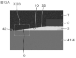
- FIG. 7 is an enlarged view of a portion surrounded by a two-dot chain line VII in FIG.
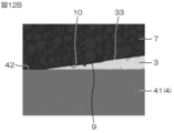
- FIG. 8 is an enlarged view of a portion surrounded by a two-dot chain line VIII in FIG.
- FIG. 9 is a flowchart of the manufacturing process of the semiconductor device.
- FIG. 9 is a flowchart of the manufacturing process of the semiconductor device.
- FIG. 10 is a diagram for explaining the generation of corrosive ions.
- 11A is an SEM image showing a main part of the semiconductor device according to Sample 1.
- FIG. 11B is an enlarged view of a portion surrounded by a two-dot chain line XIB in FIG. 11A.
- 12A is an SEM image showing a main part of a semiconductor device according to Sample 2.
- FIG. 12B is an enlarged view of a portion surrounded by a two-dot chain line XIIB in FIG. 12A.
- FIG. 13 is an SEM image for explaining the barrier layer of the semiconductor device according to Sample 2.
- FIG. FIG. 14 is an SEM image for explaining the barrier layer of the semiconductor device according to Sample 2.
- FIG. FIG. 15 is a graph showing the relationship between the number of cycles in the temperature cycle test and the thermal resistance change rate.
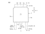
- FIG. 1 is a schematic perspective view of a semiconductor device 1 according to an embodiment of the present disclosure.
- a sealing resin 7, which will be described later, is indicated by a dashed line, and the internal structure of the semiconductor device 1 is seen through.
- FIG. 2 is a schematic front view of the semiconductor device 1.
- FIG. 3 is a schematic side view of the semiconductor device 1.
- FIG. 4 is a schematic rear view of the semiconductor device 1.
- FIG. 5 is a schematic bottom view of the semiconductor device 1.
- FIG. FIG. 6 is a diagram showing a cross section taken along line VI-VI of FIG.
- FIG. 7 is an enlarged view of a portion surrounded by a two-dot chain line VII in FIG.
- FIG. 8 is an enlarged view of a portion surrounded by a two-dot chain line VIII in FIG.
- the up-down direction in the plan view (FIG. 2) is defined as a first direction X
- the left-right direction in the plan view (FIG. 2) perpendicular to the first direction X is defined as a second direction Y.
- Both the first direction X and the second direction Y are perpendicular to the thickness direction (third direction Z) of the semiconductor device 1, a semiconductor element 2 described later, or the like.
- the semiconductor device 1 is, for example, of a type that is surface-mounted on a circuit board such as automotive electrical equipment.
- Semiconductor device 1 includes semiconductor element 2 , element bonding layer 3 , pad terminal 4 , lead terminal 5 , bonding wire 6 , sealing resin 7 and barrier layer 8 .
- the semiconductor element 2 is an element (semiconductor chip) that serves as the core of the functions of the semiconductor device 1 .
- the semiconductor element 2 is a power MOSFET discrete element (single-function semiconductor).
- the semiconductor element 2 is formed, for example, in a square shape with a side of 3.0 mm or more and 8.0 mm or less.
- the semiconductor element 2 has an element main surface 21 (first main surface), an element back surface 22 (second main surface), an electrode pad 23 , a passivation film 24 and a back surface electrode 25 .
- the element main surface 21 is the top surface of the semiconductor element 2 shown in FIGS. Referring to FIG. 1, electrode pads 23 are formed on element main surface 21 .
- the element back surface 22 is the bottom surface of the semiconductor element 2 shown in FIGS. 7 and 8, a rear surface electrode 25 is formed on the rear surface 22 of the element. In this embodiment, the back electrode 25 serves as the drain electrode of the semiconductor element 2 .
- the element main surface 21 and the element back surface 22 are both orthogonal to the thickness direction Z of the semiconductor element 2 and face opposite sides.
- the electrode pads 23 include first electrode pads 23a and second electrode pads 23b.
- Electrode pad 23 may be made of a metal containing Al, for example.
- the electrode pad 23 may be made of metal including, for example, Al--Cu alloy, Al--Si alloy, Al--Si--Cu alloy, or the like.
- the electrode pad 23 may be a pad having a laminated structure of Al--Cu/Ti.
- the first electrode pad 23 a is the source electrode of the semiconductor element 2 .
- the second electrode pad 23b is the gate electrode of the semiconductor element 2.
- a first electrode pad 23 a is formed in a substantially rectangular shape covering substantially the entire element main surface 21 .
- the second electrode pad 23b is formed in a recess 26 formed on one side of the first electrode pad 23a. Therefore, the area of the first electrode pad 23a is made larger than the area of the second electrode pad 23b.
- a bonding wire 6 is connected to the first electrode pad 23a and the second electrode pad 23b.
- passivation film 24 is a protective film for semiconductor element 2 formed to cover main surface 21 of the element.
- the passivation film 24 may be, for example, a laminate of a Si 3 N 4 layer formed by plasma CVD and a polyimide resin layer formed by coating. Both the first electrode pad 23 a and the second electrode pad 23 b are exposed from the passivation film 24 .
- element bonding layer 3 is a conductive member interposed between semiconductor element 2 and pad terminal 4 .
- the element bonding layer 3 allows the semiconductor element 2 to be mounted on the pad terminal 4 by die bonding, and ensures electrical connection between the semiconductor element 2 and the pad terminal 4 .
- the element bonding layer 3 is made of, for example, a solder alloy material, Ag sintered material, or the like.
- Solder alloy materials include, for example, high-temperature solder (for example, high-temperature solder having a solidus temperature of about 268°C or higher and 305°C or lower).
- the high-temperature solder may use, for example, Pb or Sn as a base material, and Ag, Sb, In, or the like may be blended in the base material.
- Pb or Sn may be used as a base material, and Ag, Sb, In, or the like may be blended in the base material.
- it may contain 85 wt % or more of Pb and 10 wt % or less of Sn, specifically Pb-5Sn, Pb-2Sn-2.5Ag.
- a SAC solder of Sn--Ag--Cu may be used as a high-temperature Pb-free solder.
- solder materials it is preferred to use a high temperature solder in this embodiment in which the semiconductor element 2 is a power MOSFET (power semiconductor). If the element bonding layer 3 is made of high-temperature solder, it can withstand relatively high heat generated from the power MOSFET. Further, when the surface-mounted semiconductor device 1 is mounted on an external circuit board, it is necessary to perform reflow processing (for example, reflow processing at about 260° C. using SAC solder) again. If the element bonding layer 3 is made of high-temperature solder, it can be prevented from melting during this reflow treatment.
- reflow processing for example, reflow processing at about 260° C. using SAC solder
- the pad terminal 4 is a conductive member that forms a conductive path between the semiconductor device 1 and the circuit board by being joined to the circuit board.
- Pad terminals 4 include die pads 41 in this embodiment. In the following description, the pad terminals 4 are assumed to be the die pads 41 unless otherwise required.
- the die pad 41 is made of an alloy containing Cu.
- the die pad 41 has a thickness of, for example, 1.0 mm or more and 2.0 mm or less. If the die pad 41 has a thickness of 1.0 mm or more and 2.0 mm or less, the thermal resistance of the die pad 41 can be made relatively low. Thereby, the heat dissipation of the semiconductor device 1 can be improved.
- die pad 41 is a portion on which semiconductor element 2 is mounted.
- Die pad 41 has mounting surface 42 and mounting surface 43 .
- the mounting surface 42 is the surface on which the semiconductor element 2 is mounted, and the mounting surface 43 is the surface facing away from the mounting surface 42 .
- the mounting surface 42 is the top surface of the die pad 41 shown in FIGS.
- the mounting surface 43 is the lower surface of the die pad 41 shown in FIGS. 6-8. Both the mounting surface 42 and the mounting surface 43 are flat. Both the mounting surface 42 and the mounting surface 43 may be covered with an exterior plating layer.
- the exterior plating layer provides good solder adhesion to the portions of the pad terminals 4 exposed from the sealing resin 7 when the semiconductor device 1 is surface-mounted on the circuit board by soldering by reflow, and soldering is performed. It functions to prevent erosion of the portion due to bonding.
- the element bonding layer 3 is interposed between the element back surface 22 (back surface electrode 25) and the mounting surface 42, and the die pad 41 is connected to the back surface electrode 25 via the element bonding layer 3.
- the die pad 41 (pad terminal 4 ) functions as a drain terminal of the semiconductor device 1 .
- both the mounting surface 42 and the mounting surface 43 are partially exposed from the sealing resin 7 .
- a portion of the die pad 41 that protrudes from the end surface of the sealing resin 7 (resin first side surface 73 described later) may be referred to as a protruding portion 44 of the die pad 41 .
- the element bonding layer 3 includes a body portion 31 sandwiched between the die pad 41 and the semiconductor element 2 and a peripheral portion formed around the semiconductor element 2. 32 integrally.
- the body portion 31 forms a main path of a conductive path and a heat dissipation path between the die pad 41 and the back electrode 25 in the element bonding layer 3 .
- the peripheral portion 32 may be a surplus portion of solder material protruding outside the semiconductor element 2 when the semiconductor element 2 is mounted on the die pad 41 by reflow soldering.
- the peripheral portion 32 surrounds the semiconductor element 2 .
- the peripheral portion 32 forms a sub-path of the conductive path and the heat dissipation path.
- the element bonding layer 3 may be composed only of the body part 31 without the peripheral part 32 , or part of the peripheral part 32 may be wetted to the end surface of the semiconductor element 2 .
- peripheral portion 32 of element bonding layer 3 has an inclined surface 33 inclined with respect to mounting surface 42 of die pad 41 .
- the inclined surface 33 is inclined downward from the vicinity of the lower edge corner portion 27 of the semiconductor element 2 toward the mounting surface 42 .
- the inclined surface 33 is flat and inclined at an angle ⁇ 1 of, for example, 5° or more and 45° or less with respect to the mounting surface 42 .
- the peripheral portion 32 may have a curved side surface 34 reaching the mounting surface 42 from the vicinity of the lower edge corner portion 27 of the semiconductor chip 2 instead of the flat inclined surface 33 .
- the peripheral portion 32 may have a length L of 0.1 mm or more and 2 mm or less with respect to the thickness T of the element bonding layer 3 (for example, 50 ⁇ m or more and 200 ⁇ m or less).
- the lead terminal 5 is a conductive member that forms a conductive path between the semiconductor device 1 and the circuit board by being joined to the circuit board. Referring to FIG. 1 , lead terminal 5 is arranged adjacent to pad terminal 4 in first direction X and electrically connected to electrode pad 23 . 1, 2, 4 and 5, lead terminal 5 includes a first lead terminal 51 and a second lead terminal 52 adjacent to each other in second direction Y in plan view. In this embodiment, the lead terminals 5 are made of an alloy containing Cu, like the pad terminals 4 . Moreover, in this embodiment, the lead terminal 5 has a thickness of, for example, 1.0 mm or more and 2.0 mm or less.
- a bonding wire 6 is connected to the first lead terminal 51 .
- the first lead terminal 51 is electrically connected through the bonding wire 6 to the first electrode pad 23a. Therefore, the first lead terminal 51 is the source terminal of the semiconductor device 1 .
- the first lead terminal 51 has a first pad portion 511 , a first lead portion 512 and a dummy lead portion 513 .
- the first pad portion 511 is a substantially quadrangular portion in plan view to which the bonding wire 6 is connected.
- the first pad portion 511 is flat and entirely covered with the sealing resin 7 .
- the first lead portion 512 is a substantially rectangular portion connected to the first pad portion 511 and arranged parallel to the first direction X in a plan view.
- the first lead portion 512 has a portion exposed from the sealing resin 7 . 1, 3 and 6, the exposed portion of first lead portion 512 is bent into a gull-wing shape.
- a tip portion 512a of the first lead portion 512 is a portion of the first lead terminal 51 that is joined to the circuit board. Referring to FIG.
- the dummy lead portion 513 is a substantially rectangular portion connected to the first pad portion 511 and arranged parallel to the first direction X in plan view.
- the dummy lead portion 513 extends parallel to the first lead portion 512 in the first direction X from the first pad portion 511 . Therefore, the first lead portion 512 and the dummy lead portion 513 are adjacent to each other in the second direction Y.
- Dummy lead portion 513 has a portion exposed from sealing resin 7 .
- the exposed portion of the dummy lead portion 513 is flat. Therefore, the distal end portion 513 a of the dummy lead portion 513 is located above the distal end portion 512 a of the first lead portion 512 in the third direction Z.
- the dummy lead portions 513 are not in contact with the circuit board and are cantilevered by the sealing resin 7 .
- the bonding wire 6 is connected to the second lead terminal 52 .
- the second lead terminal 52 is electrically connected through the bonding wire 6 to the second electrode pad 23b. Therefore, the second lead terminal 52 is the gate terminal of the semiconductor device 1 .
- the second lead terminal 52 has a second pad portion 521 and a second lead portion 522 .
- the second pad portion 521 is a portion having a substantially square shape in plan view to which the bonding wire 6 is connected.
- the second pad portion 521 is flat and entirely covered with the sealing resin 7 .
- the second lead portion 522 is a substantially quadrangular portion connected to the second pad portion 521 and arranged parallel to the first direction X in plan view.
- the second lead portion 522 has a portion exposed from the sealing resin 7 .
- the exposed portion of second lead portion 522 is bent into a gull-wing shape.
- the shape of the second lead portion 522 is the same as the shape of the first lead portion 512 .
- a distal end portion 522a of the second lead portion 522 is a portion of the second lead terminal 52 that is joined to the circuit board.
- the bonding wires 6 include first bonding wires 61 and second bonding wires 62 .
- first bonding wire 61 is a conductive member that connects first electrode pad 23 a and first pad portion 511 of first lead terminal 51 . Therefore, first bonding wire 61 is the source wire of semiconductor device 1 .
- the first bonding wire 61 is made of Al or an Al alloy, for example.
- the first bonding wire 61 has a diameter of, for example, 250 ⁇ m or more and 500 ⁇ m or less.
- the second bonding wire 62 is a conductive member that connects the second electrode pad 23 b and the second pad portion 521 of the second lead terminal 52 .
- the second bonding wire 62 is the gate wire of the semiconductor device 1 .
- the second bonding wire 62 is made of Al or an Al alloy, for example.
- the second bonding wire 62 is thinner than the first bonding wire 61 and has a diameter of 100 ⁇ m or more and 200 ⁇ m or less, for example.
- the sealing resin 7 is made of black resin having electrical insulation.
- the sealing resin 7 includes, for example, a thermosetting resin such as an epoxy resin as a matrix resin (base resin), a filler, a silane coupling agent as an additive, a curing agent, a curing accelerator, and the like.
- fillers include silica filler, talc, clay, glass beads, glass fiber and the like.
- the silane coupling agent has, for example, a function of improving adhesion between the organic surface of the sealing resin 7 and the inorganic surface such as glass or metal.
- Examples of curing agents include amine-based curing agents, acid anhydride-based curing agents, phenol resins, amino resins, and the like.
- curing accelerators include phosphorus-based curing accelerators, tertiary amine-based curing accelerators, and imidazole-based curing accelerators. In this embodiment, a phosphorus accelerator is used.
- the sealing resin 7 partially covers the pad terminals 4 and the lead terminals 5 as well as the semiconductor element 2 and the bonding wires 6 .
- the sealing resin 7 is formed by transfer molding using a mold.
- the sealing resin 7 has a resin main surface 71 , a resin back surface 72 , a resin first side surface 73 , a resin second side surface 74 and a resin inner surface 75 .
- the resin main surface 71 is the top surface of the sealing resin 7 shown in FIGS.
- the resin back surface 72 is the bottom surface of the sealing resin 7 shown in FIGS.
- the resin main surface 71 and the resin back surface 72 are both orthogonal to the thickness direction Z of the semiconductor device 1 and face opposite sides. In this embodiment, the mounting surface 43 is exposed from the resin back surface 72 .
- the first resin side surfaces 73 are a pair of surfaces that are spaced apart in the first direction X.
- the pair of resin first side surfaces 73 face opposite sides.
- the upper end of the resin first side surface 73 is connected to the resin main surface 71
- the lower end of the resin first side surface 73 is connected to the resin back surface 72 .
- a part of each of the first lead terminal 51 and the second lead terminal 52 is exposed from one resin first side surface 73 . 2 to 4, the projecting portion 44 of the die pad 41 is exposed from the resin first side surface 73 on the other side.
- the resin second side surfaces 74 are a pair of surfaces spaced apart in the second direction Y.
- the pair of resin second side surfaces 74 face opposite sides.
- the upper end of the resin second side surface 74 is connected to the resin main surface 71
- the lower end of the resin second side surface 74 is connected to the resin back surface 72 .
- the pad terminal 4 or the lead terminal 5 is not exposed from the resin second side surface 74 .
- the resin inner surface 75 is either a surface where the sealing resin 7 contacts the internal structure covered with the sealing resin 7 or a surface facing the internal structure through a space such as a gap 9 to be described later.
- the surface in contact with the internal structure broadly includes the case where a space such as a gap is not formed between the internal structure, the surface in direct contact with the internal structure, and the intermediate layer such as the barrier layer 8. may also include surfaces that are in indirect contact with each other.
- the resin inner surface 75 is a first inner surface 751 which is a contact surface between the sealing resin 7 and the semiconductor element 2, and a contact surface between the sealing resin 7 and the element bonding layer 3.
- a second inner surface 752 a third inner surface 753 that is a contact surface between the sealing resin 7 and the pad terminal 4 (die pad 41 ), and a fourth inner surface 754 that is a contact surface between the sealing resin 7 and the lead terminal 5 .
- a fifth inner surface 755 that is a contact surface between the sealing resin 7 and the bonding wire 6 .
- gap 9 extending from the end surface of sealing resin 7 (in this embodiment, first resin side surface 73 having projecting portion 44 formed thereon) toward semiconductor element 2 is provided.
- the gap 9 extends upward along the mounting surface 42 of the die pad 41 and the inclined surface 33 of the element bonding layer 3 from the resin first side surface 73 of the sealing resin 7 in a cross-sectional view.
- the tip portion 91 corresponds to the dead end of the gap 9 when the resin first side surface 73 of the sealing resin 7 is used as the entrance of the gap 9 .
- the resin inner surface 75 facing the die pad 41 and the element bonding layer 3 through the gap 9 may be the sixth inner surface 756 .
- the sixth inner surface 756 is separated from the die pad 41 and the element bonding layer 3 across the gap 9 . Therefore, on the inclined surface 33 of the element bonding layer 3 , the area from the lower edge corner 27 of the semiconductor element 2 to the middle of the inclined surface 33 is the second inner surface 752 . 42 is the sixth inner surface 756 .
- the surfaces (first to fifth inner surfaces 751 to 755 in this embodiment) in contact with the internal structure such as the semiconductor element 2 and the die pad 41 in the sealing resin 7 are collectively referred to as It may be defined as an internal resin contact surface, and a surface separated from the internal structure via a space such as the gap 9 (the sixth internal surface 756 in this embodiment) may be generically defined as an internal resin separation surface.
- the barrier layer 8 is made of a material having a function of blocking corrosive ions derived from the sealing resin 7 from contacting the element bonding layer 3 .
- the corrosive ions are ions that can attack and corrode the device bonding layer 3 .
- ions that are inherently contained in the sealing resin 7 and ions that are generated due to chemical changes or alterations in the constituent substances of the sealing resin 7 can be used.
- SiO 3 H ions derived from silane coupling agents, PO 3 ions derived from phosphorus curing accelerators, COOH ions generated by oxidation of epoxy resins, and the like can be mentioned.
- constituent substances of the element bonding layer 3 are easily ionized (for example, Pb is ionized into Pb ions), the element bonding layer 3 is electrochemically corroded, and voids are formed in the element bonding layer 3. or cracks may occur.
- the barrier layer 8 that prevent such voids and cracks include aluminum oxide (Al 2 O 3 ), silicon oxide (SiO 2 ), zirconium oxide (ZrO 2 ), tantalum pentoxide (Ta 2 O 5 ), hafnium dioxide (HfO 2 ), yttrium oxide (Y 2 O 3 ) and multilayer structures thereof.
- Al 2 O 3 is used in this embodiment.
- the barrier layer 8 may have a thickness of 50 nm or more and 10 ⁇ m or less.
- barrier layer 8 protects the internal structure of semiconductor element 2, element bonding layer 3, pad terminal 4 (die pad 41), lead terminal 5, bonding wire 6, etc. in sealing resin 7. It is formed so as to cover the whole. 6 to 8 of the semiconductor element 2, the pad terminal 4 (die pad 41), the element bonding layer 3, and the lead terminal 5 inside the sealing resin 7 are covered with the barrier layer 8. .
- the barrier layer 8 does not cover the protruding portion 44 of the die pad 41 and the exposed portions of the lead terminals 5 outside the sealing resin 7 .
- a conductive terminal surface for ensuring conduction with the circuit board is ensured in the pad terminal 4 (die pad 41) and the lead terminal 5 in the outer portion of the sealing resin 7. As shown in FIG.
- barrier layer 8 forms boundary portion 10 between element bonding layer 3 (peripheral portion 32 ) and sealing resin 7 .
- a part of the barrier layer 8 is held in close contact with the resin inner surface 75 of the sealing resin 7 while floating from the die pad 41 via the gap 9 .
- the barrier layer 8 seals between the separation portion 81 floating from the die pad 41 and the element bonding layer 3 through the gap 9 and between the lower edge corner portion 27 of the semiconductor element 2 and the tip portion 91 of the gap 9 .
- a sandwiching portion 82 sandwiched between the sealing resin 7 and the element bonding layer 3 may be included.
- FIG. 9 is a flowchart showing an example of the manufacturing process of the semiconductor device 1. As shown in FIG.
- the method of manufacturing semiconductor device 1 mainly includes component preparation step S1, die bonding step S2, wire bonding step S3, barrier layer forming step S4, resin sealing step S5 and final step S6. You can stay.
- the method for manufacturing the semiconductor device 1 may include steps not shown in FIG.
- the component preparation step S1 is a step of preparing each component of the semiconductor device 1 described above. For example, from a wafer of semiconductor elements 2, semiconductor elements 2 of a predetermined size are produced by dicing the wafer. Also, a lead frame in which the pad terminal 4 (die pad 41) and the lead terminal 5 are integrally connected is molded by molding.
- the die-bonding step S2 is a step of die-bonding the semiconductor element 2 .
- the die bonding step S2 is performed using, for example, a well-known die bonder, and may be called a mounting step.
- the die bonding step S2 is a step of conductively bonding the semiconductor element 2 to the die pad 41 by the element bonding layer 3 .
- a paste bonding material for example, solder paste, Ag paste, etc.
- the atmosphere temperature in the furnace is raised to the melting point of the bonding material (for example, 300° C. or more and 390° C.
- the ambient temperature in the furnace is lowered to normal temperature (below the melting point of the bonding material), and the bonding material is cured to form the element bonding layer 3 .
- the semiconductor element 2 and the die pad 41 are electrically connected.
- the wire bonding step S3 is a step of bonding the first bonding wire 61 and the second bonding wire 62.
- the wire bonding step S3 is performed using, for example, a known wire bonder.
- the wire bonding step S3 uses the wire bonder to perform wire bonding between one end of the first bonding wire 61 and the first electrode pad 23a and wire bonding between the other end of the first bonding wire 61 and the first pad portion 511. including the step of performing Specifically, first, the tip of the wire is protruded from the capillary of the wire bonder and melted to form the tip of the wire into a ball shape. Then, the tip portion is pressed against the first electrode pad 23a.
- the wire bonding step S3 uses the wire bonder to perform wire bonding between one end of the second bonding wire 62 and the second electrode pad 23b, and wire bonding of the other end of the second bonding wire 62 and the second pad portion. 521 is included.
- all wire joints may be wedge bonds.
- a wedge bond is formed by pressing a wire into place and cutting the wire.
- each wire bonding portion may be distinguished from the first bonding and the second bonding according to the order in which the wires are bonded.
- the first electrode pad 23a and the second electrode pad 23b are first-bonded, and the first pad portion 511 and the second pad portion 521 are second-bonded.
- the first bonding may be performed on the first pad portion 511 and the second pad portion 521, and the second bonding may be performed on the first electrode pad 23a and the second electrode pad 23b.
- the barrier layer forming step S4 is a step of covering the semiconductor element 2, the element bonding layer 3, the pad terminal 4 (die pad 41), the lead terminal 5 and the bonding wire 6 with the barrier layer 8.
- FIG. The barrier layer forming step S4 is performed by, for example, a well-known film forming method.
- an Al 2 O 3 film is formed by an ion plating method, a sputtering method, or the like.
- the film forming temperature of the barrier layer 8 may be, for example, room temperature or higher and 300° C. or lower.
- the resin sealing step S5 is a step of forming the sealing resin 7 and packaging the semiconductor device 1 . That is, the resin sealing step S5 is a step of forming the sealing resin 7 having the shape described above.
- the resin sealing step S5 is performed, for example, by well-known transfer molding using a mold. Specifically, after the barrier layer 8 is formed, the lead frame to which the semiconductor element 2 is bonded is set in a mold molding machine, and the fluidized epoxy resin is poured into the mold for molding. Then, the epoxy resin is cured, and the molded lead frame is taken out. Then, it is shaped into the shape of the above-described sealing resin 7 by removing excess resin, burrs, or the like.
- the final step S6 is a step of forming the semiconductor device 1 into the shape shown in FIG. 1 and finishing the semiconductor device 1 into a product that can be shipped.
- the final step S6 includes, for example, a step of removing burrs from the sealing resin 7, a cutting step of cutting unnecessary portions of the lead frame exposed to the outside of the sealing resin 7, and a step of bending the lead frame exposed to the outside of the sealing resin 7.
- An exterior treatment process for improving strength, improving solder wettability at the time of mounting on a circuit board or the like, preventing rust, etc., a cleaning process before the exterior treatment process, and removing the lead frame exposed to the outside of the sealing resin 7 in a predetermined manner.
- a lead processing process that bends the product into a shape, a stamping process that stamps the company name, product name, lot number, etc. on the package, and an inspection and sorting process that determines whether the product is good or not is performed. Note that these steps may be appropriately performed according to the final specifications of the semiconductor device 1 .
- the barrier layer 8 formed on the lead terminals 5 exposed to the outside of the sealing resin 7 is removed, and the exterior surfaces of the lead terminals 5 are exposed.
- the semiconductor device 1 shown in FIG. 1 is completed. [Verification of generation of corrosive ions] FIG.
- FIG. 10 is a diagram for verifying that corrosive ions are generated at the boundary 10 between the sealing resin 7 and the element bonding layer 3.
- FIG. 10 shows an optical microscope image of the boundary 10 between the sealing resin 7 and the element bonding layer 3 in the sample 1, and time-of-flight secondary ion mass spectrometry (TOF-SIMS). ) is a graphical representation of the analysis result image.
- the sealing resin 7 is an epoxy resin containing at least a silane coupling agent and a phosphorus-based curing accelerator as additives and a silica filler as filler 11 .
- the element bonding layer 3 is a high temperature solder made of Pb-2Sn-2.5Ag.
- the leftmost mass corresponds to the optical microscope image
- the other masses are the results of TOF-SIMS analysis of Si ions, Pb ions, SiO 3 H ions, PO 3 ions and COOH ions.
- Each detected fragment containing The diagrams of the detected fragments all show the analysis results of the boundary portion 10 in the same way as the optical microscope image, but for the sake of clarity, the reference numerals of the sealing resin 7 and the element bonding layer 3 are omitted. ing.
- each figure in the upper row shows the state after assembly (immediately after manufacture) of the semiconductor device of Sample 1 and before the temperature cycle test (TC) is performed.
- the lower figures show the state after the temperature cycle test (TC) was performed on the semiconductor device of Sample 1.
- FIG. In the temperature cycle test, the semiconductor device after assembly is exposed to an environment of MSL1 (Moisture Sensitivity Level 1) in accordance with IPC/JEDEC J-STD-020. It was carried out by repeating 1000 cycles of heating and cooling between.
- MSL1 Microisture Sensitivity Level 1
- the element bonding layer 3 was corroded, and that the gap 14 and the crack 12 were generated on the element bonding layer 3 side with respect to the boundary portion 10 .
- the causes of the voids 14 and the cracks 12 are the thermal stress (tensile stress) generated in the boundary portion 10 during the temperature cycle test, and the corrosive ions (corrosive stress) in the boundary portion 10 . chemical species) are generated, and it was found that the corrosive action by the corrosive ions is related.
- SiO 3 H ions, PO 3 ions and COOH ions are widely distributed in the regions where voids 14 and cracks 12 are generated, thereby ionizing Pb in the high-temperature solder and causing corrosion to progress.
- SiO 3 H ions are the source of the silane coupling agent in the sealing resin 7
- PO 3 ions are the source of the phosphorus-based curing accelerator in the sealing resin 7
- COOH ions are the source of the sealing resin 7 .
- the epoxy resin of is produced by oxidation.
- the generation of corrosive ions in the boundary portion 10 under the conditions that the voids 14 and the cracks 12 are likely to occur due to the thermal stress during the temperature cycle test causes the alloy of the element bonding layer 3 (solder alloy) to It is considered that the compositional balance of is disturbed, and the generation of voids 14 and cracks 12 is accelerated.
- FIG. 11A is an SEM image showing a main part of the semiconductor device according to Sample 1.
- FIG. 11B is an SEM image showing a main part of the semiconductor device according to Sample 1.
- FIG. 11B is an enlarged view of a portion surrounded by a two-dot chain line XIB in FIG. 11A.
- 12A is an SEM image showing a main part of a semiconductor device according to Sample 2.
- FIG. 12B is an enlarged view of a portion surrounded by a two-dot chain line XIIB in FIG. 12A.
- FIG. 13 is an SEM image for explaining the barrier layer 8 of the semiconductor device according to Sample 2.
- FIG. FIG. 14 is an SEM image for explaining the barrier layer 8 of the semiconductor device according to Sample 2.
- FIG. FIG. 15 is a graph showing the relationship between the number of cycles in the temperature cycle test and the thermal resistance change rate.
- Sample 2 which is to be compared with Sample 1, has a barrier layer 8 (Al 2 O 3 layer) between the sealing resin 7, the die pad 41 (pad terminal 4) and the element bonding layer 3, except that: It has the same structure as sample 1. As shown in FIG. 13, in sample 2, barrier layer 8 sandwiched between sealing resin 7 and element bonding layer 3 can be confirmed. That is, the overall structure of Sample 2 is the same as the structure shown in FIGS. 1-8.
- FIGS. 11A and 11B are SEM images after 750 cycles of the temperature cycle test described above.
- FIGS. 11A and 11B since the barrier layer 8 is not formed in the sample 1, a large gap 14 is formed in the boundary portion 10 between the sealing resin 7 and the element bonding layer 3, and the element bonding is performed from the gap 14. Cracks 12 extending into the interior of layer 3 were confirmed. The gaps 14 and the cracks 12 are distributed over the entire inclined surface 33 of the element bonding layer 3 , and the cracks 12 form the conductive paths and the heat dissipation paths between the semiconductor element 2 and the element bonding layer 3 immediately below the semiconductor element 2 .
- FIGS. 12A and 12B no conspicuous voids 14 or cracks 12 were observed even after 750 cycles of the temperature cycle test.
- a gap 9 is formed between the sealing resin 7 and the element bonding layer 3 due to interfacial peeling, but the peeling stops halfway along the inclined surface 33 of the element bonding layer 3 .
- the barrier layer 8 was held in close contact with the internal resin surface of the sealing resin 7 while floating from the die pad 41 in the gap 9 (see also FIG. 8). See also).
- the sealing resin 7 of sample 2 did not show discoloration like that seen in sample 1 even after the temperature cycle test.
- the barrier layer 8 is formed between the sealing resin 7 and the element bonding layer 3, contact between the corrosive ions and the element bonding layer 3 is suppressed. can be prevented. Accordingly, corrosion of the element bonding layer 3 can be suppressed, and weakening of the strength of the element bonding layer 3 can be suppressed. As a result, cracks in the element bonding layer 3 can be suppressed even if stress is applied to the element bonding layer 3 , so that deterioration of heat dissipation through the element bonding layer 3 can be suppressed.
- the electrical resistance is as low as possible.
- various members for example, pad terminals 4, lead terminals 5, bonding wires 6, etc.
- the barrier layer 8 can suppress the corrosion of the element bonding layer 3 , and can suppress the weakening of the strength of the element bonding layer 3 . Therefore, even if a large stress is applied to the element bonding layer 3, it is possible to suppress the occurrence of cracks over a wide area.
- the semiconductor device 1 is surface-mounted on a circuit board or the like via a pad terminal 4 (die pad 41) that is a drain terminal.
- the surface mount type semiconductor device 1 is mounted by reflowing a bonding material for attachment to a circuit board (for example, paste for attachment such as Pb-free solder). Thermal stress is more likely to be applied to the element bonding layer 3 from the attachment bonding material via the die pad 41 in the surface-mounted semiconductor device 1 than in the flow-mounted semiconductor device having pin terminals.
- the barrier layer 8 can prevent the strength of the element bonding layer 3 from weakening, as described above. Therefore, it is possible to suppress the occurrence of cracks due to the thermal stress applied to the element bonding layer 3, so that it is possible to provide a power semiconductor having high heat dissipation reliability.
- a gap 9 is formed at the base end of the protruding portion 44 so as to extend from the first resin side surface 73 of the sealing resin 7 to the inside of the sealing resin 7 . That is, the space 9 is formed between the resin inner surface 75 of the sealing resin 7 and the die pad 41 , and the environment is such that oxygen and moisture easily enter the inside of the sealing resin 7 . Therefore, oxygen enters between the sealing resin 7 and the element bonding layer 3, and an environment may be created in which a part of the sealing resin 7 (epoxy resin) is oxidized to generate corrosive ions. However, the barrier layer 8 is in close contact with the resin inner surface 75 of the sealing resin 7 . As a result, even if oxygen or moisture enters the gap 9, contact between the sealing resin 7 and oxygen or moisture can be effectively prevented, and generation of corrosive ions derived from the sealing resin 7 can be suppressed. .
- this type of crack is formed by a crack 12 extending in the lateral direction directly under the semiconductor element 2 so as to divide the conductive path and the heat radiation path between the semiconductor element 2 and the element bonding layer 3. Applicable.
- the gap 9 extending from the resin first side surface 73 of the sealing resin 7 does not reach the lower edge corner portion 27 of the semiconductor element 2 .
- FIG. 15 is a graph showing the relationship between the number of cycles in the temperature cycle test and the rate of change in thermal resistance for samples 1 and 2. As shown in FIG. With reference to FIG. 15, it will be verified to what extent the formation of the barrier layer 8 suppresses heat dissipation.
- FIG. 15 shows the rate of thermal resistance change at 300, 500, 750 and 1000 cycles with respect to the thermal resistance (0%) of the semiconductor device before the temperature cycle test for Samples 1 and 2 described above. ing.
- the rate of change in thermal resistance of the semiconductor device starts to increase after about 200 cycles, and increases sharply after about 500 cycles.
- the thermal resistance change rate increases after 500 cycles, but the thermal resistance change rate at 1000 cycles is about 10%, which is about 30% for sample 1.
- a much lower thermal resistivity could be maintained. From this verification result, it can be seen that the formation of the barrier layer 8 can suppress the occurrence of cracks in the element bonding layer 3 and suppress the deterioration of heat dissipation.
- the barrier layer (8) is formed between the sealing resin (7) and the element bonding layer (3), contact between corrosive ions and the element bonding layer (3) is prevented. can do. Thereby, corrosion of the element bonding layer (3) can be suppressed, and weakening of the strength of the element bonding layer (3) can be suppressed. As a result, even if stress is applied to the element bonding layer (3), cracks (12) can be prevented from occurring in the element bonding layer (3). be able to.
- the sealing resin (7) has end surfaces (73, 74) forming the peripheral contour of the sealing resin (7), According to Appendix 1-1, the die pad (41) includes a projecting portion (44) projecting outward from the sealing resin (7) starting from the end surfaces (73, 74) of the sealing resin (7)
- the sealing resin (7) has an inner surface (75) facing the semiconductor element (2), the element bonding layer (3) and the die pad (41), At least between the inner surface (75) of the sealing resin (7) and the die pad (41), there extends from end surfaces (73, 74) of the sealing resin (7) toward the semiconductor element (2) A gap (9) is formed, A part of the barrier layer (8) is held in close contact with the inner surface (75) of the sealing resin (7) while floating from the die pad (41) through the gap (9).
- the semiconductor device (1) according to Appendix 1-2, wherein:
- the gap (9) is formed between the inner surface (75) of the sealing resin (7) and the die pad (41), and oxygen and moisture are prevented from entering the sealing resin (7).
- the barrier layer (8) is in intimate contact with the inner surface (75) of the encapsulating resin (7), although it is an intrusive environment. As a result, even if oxygen or moisture enters the gap (9), contact between the sealing resin (7) and oxygen or moisture is effectively prevented, and corrosive ions derived from the sealing resin (7) are generated. can be suppressed.
- the gap (9) extends from the end surfaces (73, 74) of the sealing resin (7) along the die pad (41) and the element bonding layer (3), and extends on the element bonding layer (3). having an end (91),
- the barrier layer (8) includes a separation portion (81) floating from the die pad (41) and the element bonding layer (3) through the gap (9), and a lower edge of the semiconductor element (2). a holding portion (82) sandwiched between the sealing resin (7) and the element bonding layer (3) between the corner (27) and the end (91) of the gap (9);
- the semiconductor device (1) according to appendix 1-3, comprising:
- the crack (12) when a crack (12) occurs in the element bonding layer (3) in a region inside the semiconductor element (2) from the lower edge corner (27) of the semiconductor element (2), the crack (12) is It can be a heat dissipation resistor that transfers heat from (2) to the die pad (41) immediately below.
- the gap (9) extending from the end surfaces (73, 74) of the sealing resin (7) does not reach the lower edge corner (27) of the semiconductor element (2). Therefore, for example, even if corrosive ions originating from the outside enter the gap (9), a crack (12) occurs in the element bonding layer (3) at least in the vicinity of the lower edge corner (27) of the semiconductor element (2). can be prevented. As a result, it is possible to suppress deterioration in heat dissipation through the element bonding layer (3).
- the element bonding layer (3) is in close contact with the sealing resin (7) via the barrier layer (8) (sandwiching portion (82)), the stress applied to the element bonding layer (3) is reduced. be able to.
- the close contact between the sealing resin (7) and the element bonding layer (3) via the barrier layer (8) can also prevent cracks (12) from occurring in the element bonding layer (3).
- the element bonding layer (3) includes a body portion (31) sandwiched between the die pad (41) and the semiconductor element (2) and a peripheral portion (31) formed around the semiconductor element (2). 32), integrally including a peripheral portion (32) having an inclined surface (33) inclined with respect to the die pad (41), The gap (9) is formed so as to warp upward along the surface (42) of the die pad (41) and the inclined surface (33) of the element bonding layer (3) in a cross-sectional view.
- the semiconductor device (1) according to 1-4.
- the semiconductor element (2) has a first main surface (21) and an element rear surface (22) on the opposite side, and a gate electrode (23b) and a source electrode (23a) are provided on the first main surface (21). and a power semiconductor in which a drain electrode (25) electrically connected to the die pad (41) through the element bonding layer (3) is formed on the element back surface (22). 1.
- the semiconductor device (1) according to any one of Appendices 1-6.
- a temperature cycle test is one of the various reliability tests for semiconductor devices (1). Since a power semiconductor needs to pass a large current, it is preferable that the resistance value is as low as possible. In order to reduce the resistance, for example, various members (for example, external terminals, internal wires, etc.) that constitute the semiconductor device (1) tend to be large, and as a result, the transfer from these members to the element bonding layer (3) stress tends to increase. Therefore, cracks (12) are likely to occur in the element bonding layer (3) due to the stress. On the other hand, according to this configuration, the barrier layer (8) can suppress corrosion of the element bonding layer (3), and can suppress weakening of the element bonding layer (3). Therefore, even if a large stress is applied to the element bonding layer (3), cracks (12) can be prevented from occurring over a wide area.
- various members for example, external terminals, internal wires, etc.
- the die pad (41) is exposed from the sealing resin (7) as a drain terminal (4) on a mounting surface (42) on which the semiconductor element (2) is mounted and on the side opposite to the mounting surface (42). a mounting surface (43); a source lead terminal (51) electrically connected to the source electrode (23a) in the sealing resin (7) and exposed from the sealing resin (7); and a gate lead terminal (52) electrically connected to the gate electrode (23b) within the sealing resin (7) and exposed from the sealing resin (7).
- a semiconductor device (1) is exposed from the sealing resin (7) as a drain terminal (4) on a mounting surface (42) on which the semiconductor element (2) is mounted and on the side opposite to the mounting surface (42). a mounting surface (43); a source lead terminal (51) electrically connected to the source electrode (23a) in the sealing resin (7) and exposed from the sealing resin (7); and a gate lead terminal (52) electrically connected to the gate electrode (23b) within the sealing resin (7) and exposed from the sealing resin (7).
- the semiconductor device (1) can be surface-mounted on a circuit board or the like through the die pad (41) which is the drain terminal (4).
- a surface mount type semiconductor device (1) is mounted by reflowing a bonding material for attachment (for example, paste for attachment) to a circuit board.
- stress is applied to the element bonding layer (3) from the attachment bonding material through the die pad (41), compared to the semiconductor device having pin terminals mounted by the flow method.
- the barrier layer (8) can suppress the occurrence of cracks (12) due to the stress applied to the element bonding layer (3).
- a semiconductor can be provided.
- the die pad (41) has a thickness of 1.0 mm or more and 2.0 mm or less, so the thermal resistance of the die pad (41) can be relatively low. Thereby, the heat dissipation of the semiconductor device (1) can be improved.
- Appendix 1-12 The semiconductor device (1) according to any one of Appendixes 1-1 to 1-11, wherein the device bonding layer (3) includes a device bonding layer (3) containing a solder alloy.
- the barrier layer (8) can block the contact between the corrosive ions and the element bonding layer (3), so that it is possible to suppress the breakdown of the compositional balance of the alloy. As a result, it is possible to prevent the element bonding layer (3) from weakening in terms of strength.
- thermosetting base resin comprises an epoxy resin
- Appendix 1-16 The semiconductor device according to any one of Appendixes 1-1 to 1-15, wherein the element bonding layer (3) has a thickness of 50 ⁇ m or more and 200 ⁇ m or less.
- Appendix 1-17 The semiconductor device according to any one of Appendixes 1-1 to 1-16, wherein the barrier layer (8) has a thickness of 50 nm or more and 10 ⁇ m or less.
- Reference Signs List 1 Semiconductor device 2 : Semiconductor element 3 : Element bonding layer 4 : Pad terminal 5 : Lead terminal 6 : Bonding wire 7 : Sealing resin 8 : Barrier layer 9 : Gap 10 : Boundary 11 : Filler 12 : Crack 13 : Distribution area 14 : Gap 21 : Element main surface 22 : Element back surface 23 : Electrode pad 23a : First electrode pad 23b : Second electrode pad 24 : Passivation film 25 : Back surface electrode 26 : Concave portion 27 : Lower edge corner 31 : Main body Part 32 : Peripheral part 33 : Inclined surface 34 : Side surface 41 : Die pad 42 : Mounting surface 43 : Mounting surface 44 : Projecting portion 51 : First lead terminal 52 : Second lead terminal 61 : First bonding wire 62 : Second bonding Wire 71 : Resin main surface 72 : Resin back surface 73 : Resin first side surface 74 : Resin second side
Abstract
A semiconductor device that includes: a die pad; a semiconductor element disposed upon the die pad; an element-joining layer that is formed between the die pad and the semiconductor element and joins the die pad and the semiconductor element; a sealing resin that covers the die pad, the semiconductor element, and the element-joining layer; and a barrier layer that is formed at the boundary of the sealing resin and the element-joining layer and blocks corrosive ions derived from the sealing resin. The sealing resin has an end surface that forms a circumferential outer shape for sealing resin and the die pad may include a protruding section on the outside of the sealing resin, starting from the end surface of the sealing resin.
Description
本開示は、半導体装置に関する。
The present disclosure relates to semiconductor devices.
たとえば、特許文献1は、素子主面に電極パッドが形成された半導体素子と、半導体素子を搭載し、かつ素子裏面に導通する中間端子と、中間端子に隣接して配置され、かつ電極パッドに導通する側方端子と、電極パッドと側方端子とを接続する金属板と、電極パッドと金属板との間に介在する接合層と、半導体素子を覆う封止樹脂と、を備え、金属板は、電極パッドに接続される素子接続部と、側方端子に接続される端子接続部と、素子接続部と端子接続部との間に位置する中間部と、を有し、素子接続部に突起が形成されている、半導体装置を開示している。
For example, Patent Document 1 discloses a semiconductor element having an electrode pad formed on the main surface of the element, an intermediate terminal on which the semiconductor element is mounted and which is electrically connected to the back surface of the element, and an intermediate terminal arranged adjacent to the intermediate terminal and connected to the electrode pad. A metal plate comprising: a conductive side terminal; a metal plate connecting the electrode pad and the side terminal; a bonding layer interposed between the electrode pad and the metal plate; and a sealing resin covering a semiconductor element; has an element connection portion connected to the electrode pad, a terminal connection portion connected to the side terminal, and an intermediate portion located between the element connection portion and the terminal connection portion, and the element connection portion Disclosed is a semiconductor device in which a protrusion is formed.
本開示の一実施形態は、素子接合層にクラックが発生することを抑制することによって放熱性の低下を抑制することができる半導体装置を提供する。
An embodiment of the present disclosure provides a semiconductor device capable of suppressing deterioration in heat dissipation by suppressing cracks in the element bonding layer.
本開示の一実施形態に係る半導体装置は、ダイパッドと、前記ダイパッド上に配置された半導体素子と、前記ダイパッドと前記半導体素子との間に形成され、前記ダイパッドに前記半導体素子を接合する素子接合層と、前記ダイパッド、前記半導体素子および前記素子接合層を覆う封止樹脂と、前記封止樹脂と前記素子接合層との境界部に形成され、前記封止樹脂由来の腐食性イオンをブロックするバリア層とを含む。
A semiconductor device according to an embodiment of the present disclosure includes a die pad, a semiconductor element arranged on the die pad, and an element bonding device formed between the die pad and the semiconductor element for bonding the semiconductor element to the die pad. a layer, a sealing resin that covers the die pad, the semiconductor element and the element bonding layer, and a boundary portion between the sealing resin and the element bonding layer to block corrosive ions derived from the sealing resin. and a barrier layer.
本開示の一実施形態に係る半導体装置によれば、素子接合層にクラックが発生することを抑制できるので、素子接合層を介する放熱性の低下を抑制することができる。
According to the semiconductor device according to the embodiment of the present disclosure, it is possible to suppress the occurrence of cracks in the element bonding layer, so it is possible to suppress deterioration in heat dissipation through the element bonding layer.
次に、本開示の実施形態を、添付図面を参照して詳細に説明する。
[半導体装置1の構成]
まず、図1~図8を参照して、本開示の一実施形態に係る半導体装置1の構造について説明する。図1は、本開示の一実施形態に係る半導体装置1の模式的な斜視図である。図1では、明瞭化のため、後述する封止樹脂7を破線で示し、半導体装置1の内部構造を透視して示している。図2は、半導体装置1の模式的な正面図である。図3は、半導体装置1の模式的な側面図である。図4は、半導体装置1の模式的な背面図である。図5は、半導体装置1の模式的な底面図である。図6は、図2のVI-VI線における断面を示す図である。図7は、図6の二点鎖線VIIで囲まれた部分の拡大図である。図8は、図7の二点鎖線VIIIで囲まれた部分の拡大図である。 Embodiments of the present disclosure will now be described in detail with reference to the accompanying drawings.
[Structure of semiconductor device 1]
First, the structure of asemiconductor device 1 according to an embodiment of the present disclosure will be described with reference to FIGS. 1 to 8. FIG. FIG. 1 is a schematic perspective view of a semiconductor device 1 according to an embodiment of the present disclosure. In FIG. 1, for clarity, a sealing resin 7, which will be described later, is indicated by a dashed line, and the internal structure of the semiconductor device 1 is seen through. FIG. 2 is a schematic front view of the semiconductor device 1. FIG. FIG. 3 is a schematic side view of the semiconductor device 1. FIG. FIG. 4 is a schematic rear view of the semiconductor device 1. FIG. FIG. 5 is a schematic bottom view of the semiconductor device 1. FIG. FIG. 6 is a diagram showing a cross section taken along line VI-VI of FIG. FIG. 7 is an enlarged view of a portion surrounded by a two-dot chain line VII in FIG. FIG. 8 is an enlarged view of a portion surrounded by a two-dot chain line VIII in FIG.
[半導体装置1の構成]
まず、図1~図8を参照して、本開示の一実施形態に係る半導体装置1の構造について説明する。図1は、本開示の一実施形態に係る半導体装置1の模式的な斜視図である。図1では、明瞭化のため、後述する封止樹脂7を破線で示し、半導体装置1の内部構造を透視して示している。図2は、半導体装置1の模式的な正面図である。図3は、半導体装置1の模式的な側面図である。図4は、半導体装置1の模式的な背面図である。図5は、半導体装置1の模式的な底面図である。図6は、図2のVI-VI線における断面を示す図である。図7は、図6の二点鎖線VIIで囲まれた部分の拡大図である。図8は、図7の二点鎖線VIIIで囲まれた部分の拡大図である。 Embodiments of the present disclosure will now be described in detail with reference to the accompanying drawings.
[Structure of semiconductor device 1]
First, the structure of a
以下の説明では、平面図(図2)の上下方向を第1方向Xと定義し、第1方向Xに対して直角である平面図(図2)の左右方向を第2方向Yと定義する。第1方向Xおよび第2方向Yは、いずれも半導体装置1や後述する半導体素子2等の厚さ方向(第3方向Z)に対して直角である。
In the following description, the up-down direction in the plan view (FIG. 2) is defined as a first direction X, and the left-right direction in the plan view (FIG. 2) perpendicular to the first direction X is defined as a second direction Y. . Both the first direction X and the second direction Y are perpendicular to the thickness direction (third direction Z) of the semiconductor device 1, a semiconductor element 2 described later, or the like.
半導体装置1は、たとえば、自動車電装等の回路基板に表面実装される形式のものである。半導体装置1は、半導体素子2、素子接合層3、パッド端子4、リード端子5、ボンディングワイヤ6、封止樹脂7およびバリア層8を含む。
The semiconductor device 1 is, for example, of a type that is surface-mounted on a circuit board such as automotive electrical equipment. Semiconductor device 1 includes semiconductor element 2 , element bonding layer 3 , pad terminal 4 , lead terminal 5 , bonding wire 6 , sealing resin 7 and barrier layer 8 .
半導体素子2は、半導体装置1の機能の中枢となる素子(半導体チップ)である。この実施形態では、半導体素子2は、パワーMOSFETのディスクリート素子(単機能半導体)である。半導体素子2は、たとえば、一辺が3.0mm以上8.0mm以下の四角形状に形成されている。半導体素子2は、素子主面21(第1主面)、素子裏面22(第2主面)、電極パッド23、パッシベーション膜24および裏面電極25を有する。
The semiconductor element 2 is an element (semiconductor chip) that serves as the core of the functions of the semiconductor device 1 . In this embodiment, the semiconductor element 2 is a power MOSFET discrete element (single-function semiconductor). The semiconductor element 2 is formed, for example, in a square shape with a side of 3.0 mm or more and 8.0 mm or less. The semiconductor element 2 has an element main surface 21 (first main surface), an element back surface 22 (second main surface), an electrode pad 23 , a passivation film 24 and a back surface electrode 25 .
素子主面21は、図6~図8に示す半導体素子2の上面である。図1を参照して、素子主面21に電極パッド23が形成されている。素子裏面22は、図6~図8に示す半導体素子2の下面である。図7および図8を参照して、素子裏面22に裏面電極25が形成されている。この実施形態では、裏面電極25は半導体素子2のドレイン電極となっている。素子主面21および素子裏面22は、ともに半導体素子2の厚さ方向Zに対して直交し、かつ互いに反対側を向いている。
The element main surface 21 is the top surface of the semiconductor element 2 shown in FIGS. Referring to FIG. 1, electrode pads 23 are formed on element main surface 21 . The element back surface 22 is the bottom surface of the semiconductor element 2 shown in FIGS. 7 and 8, a rear surface electrode 25 is formed on the rear surface 22 of the element. In this embodiment, the back electrode 25 serves as the drain electrode of the semiconductor element 2 . The element main surface 21 and the element back surface 22 are both orthogonal to the thickness direction Z of the semiconductor element 2 and face opposite sides.
図1を参照して、電極パッド23は、第1電極パッド23aおよび第2電極パッド23bを含む。電極パッド23は、たとえば、Alを含む金属で形成されていてもよい。電極パッド23は、たとえば、Al-Cu合金、Al-Si合金、Al-Si-Cu合金等を含む金属で形成されていてもよい。具体的な一例としては、電極パッド23は、Al-Cu/Tiの積層構造からなるパッドであってもよい。この実施形態では、第1電極パッド23aは、半導体素子2のソース電極である。この実施形態では、第2電極パッド23bは、半導体素子2のゲート電極である。第1電極パッド23aが素子主面21のほぼ全体を覆う略四角形状に形成されている。第2電極パッド23bは、第1電極パッド23aの一辺に形成された凹部26に形成されている。したがって、第1電極パッド23aの面積は、第2電極パッド23bの面積よりも大とされている。第1電極パッド23aおよび第2電極パッド23bには、ボンディングワイヤ6が接続されている。
Referring to FIG. 1, the electrode pads 23 include first electrode pads 23a and second electrode pads 23b. Electrode pad 23 may be made of a metal containing Al, for example. The electrode pad 23 may be made of metal including, for example, Al--Cu alloy, Al--Si alloy, Al--Si--Cu alloy, or the like. As a specific example, the electrode pad 23 may be a pad having a laminated structure of Al--Cu/Ti. In this embodiment, the first electrode pad 23 a is the source electrode of the semiconductor element 2 . In this embodiment, the second electrode pad 23b is the gate electrode of the semiconductor element 2. As shown in FIG. A first electrode pad 23 a is formed in a substantially rectangular shape covering substantially the entire element main surface 21 . The second electrode pad 23b is formed in a recess 26 formed on one side of the first electrode pad 23a. Therefore, the area of the first electrode pad 23a is made larger than the area of the second electrode pad 23b. A bonding wire 6 is connected to the first electrode pad 23a and the second electrode pad 23b.
図1を参照して、パッシベーション膜24は、素子主面21を覆うように形成された半導体素子2の保護膜である。パッシベーション膜24は、たとえばプラズマCVD法によって形成されたSi3N4層と、塗布によって形成されたポリイミド樹脂層とが互いに積層されたものであってもよい。パッシベーション膜24から、第1電極パッド23aおよび第2電極パッド23bがともに露出している。
Referring to FIG. 1, passivation film 24 is a protective film for semiconductor element 2 formed to cover main surface 21 of the element. The passivation film 24 may be, for example, a laminate of a Si 3 N 4 layer formed by plasma CVD and a polyimide resin layer formed by coating. Both the first electrode pad 23 a and the second electrode pad 23 b are exposed from the passivation film 24 .
図1、図7および図8を参照して、素子接合層3は、半導体素子2とパッド端子4との間に介在する、導電性を有した部材である。素子接合層3によって、半導体素子2はパッド端子4にダイボンディングによって搭載され、かつ半導体素子2とパッド端子4との導通が確保される。素子接合層3は、たとえば、はんだ合金材、Ag焼結材等からなる。
1, 7 and 8, element bonding layer 3 is a conductive member interposed between semiconductor element 2 and pad terminal 4 . The element bonding layer 3 allows the semiconductor element 2 to be mounted on the pad terminal 4 by die bonding, and ensures electrical connection between the semiconductor element 2 and the pad terminal 4 . The element bonding layer 3 is made of, for example, a solder alloy material, Ag sintered material, or the like.
はんだ合金材としては、たとえば、高温はんだ(たとえば、268℃以上305℃以下程度の固相線温度を有する高温はんだ)が挙げられる。高温はんだは、たとえば、PbまたはSnをベース材料とし、当該ベース材料にAg、Sb、In等が配合されていてもよい。たとえば、85wt%以上のPb、および10wt%以下のSnを含んでいてもよく、具体的には、Pb-5Sn、Pb-2Sn-2.5Agであってもよい。また、高温のPbフリーはんだとして、Sn-Ag-CuであるSAC系はんだを使用してもよい。これらのはんだ材料のうち、半導体素子2がパワーMOSFET(パワー半導体)であるこの実施形態では、高温はんだを使用することが好ましい。素子接合層3が高温はんだであれば、パワーMOSFETから発生する比較的高い熱に耐えることができる。また、表面実装型の半導体装置1を外部の回路基板に実装する際、再度リフロー処理(たとえば、SAC系はんだを使用して260℃程度のリフロー処理)を実施する必要がある。素子接合層3が高温はんだであれば、このリフロー処理の際に溶融することを防止することができる。
Solder alloy materials include, for example, high-temperature solder (for example, high-temperature solder having a solidus temperature of about 268°C or higher and 305°C or lower). The high-temperature solder may use, for example, Pb or Sn as a base material, and Ag, Sb, In, or the like may be blended in the base material. For example, it may contain 85 wt % or more of Pb and 10 wt % or less of Sn, specifically Pb-5Sn, Pb-2Sn-2.5Ag. Also, as a high-temperature Pb-free solder, a SAC solder of Sn--Ag--Cu may be used. Of these solder materials, it is preferred to use a high temperature solder in this embodiment in which the semiconductor element 2 is a power MOSFET (power semiconductor). If the element bonding layer 3 is made of high-temperature solder, it can withstand relatively high heat generated from the power MOSFET. Further, when the surface-mounted semiconductor device 1 is mounted on an external circuit board, it is necessary to perform reflow processing (for example, reflow processing at about 260° C. using SAC solder) again. If the element bonding layer 3 is made of high-temperature solder, it can be prevented from melting during this reflow treatment.
パッド端子4は、回路基板に接合されることによって半導体装置1と前記回路基板との導電経路を構成する、導電性を有した部材である。パッド端子4は、この実施形態では、ダイパッド41を含む。以下では、特に必要な場合を除いて、パッド端子4をダイパッド41として説明する。この実施形態では、ダイパッド41は、Cuを含む合金からなる。また、この実施形態では、ダイパッド41は、たとえば、1.0mm以上2.0mm以下の厚さを有している。ダイパッド41が1.0mm以上2.0mm以下の厚さを有していれば、ダイパッド41の熱抵抗を比較的に低くすることができる。これにより、半導体装置1の放熱性を向上させることができる。
The pad terminal 4 is a conductive member that forms a conductive path between the semiconductor device 1 and the circuit board by being joined to the circuit board. Pad terminals 4 include die pads 41 in this embodiment. In the following description, the pad terminals 4 are assumed to be the die pads 41 unless otherwise required. In this embodiment, the die pad 41 is made of an alloy containing Cu. Also, in this embodiment, the die pad 41 has a thickness of, for example, 1.0 mm or more and 2.0 mm or less. If the die pad 41 has a thickness of 1.0 mm or more and 2.0 mm or less, the thermal resistance of the die pad 41 can be made relatively low. Thereby, the heat dissipation of the semiconductor device 1 can be improved.
図1および図6~図8を参照して、ダイパッド41は、半導体素子2を搭載する部位である。ダイパッド41は、搭載面42および実装面43を有する。搭載面42は、半導体素子2が搭載された面であり、実装面43は、搭載面42に対して反対側を向く面である。搭載面42は、図6~図8に示すダイパッド41の上面である。実装面43は、図6~図8に示すダイパッド41の下面である。搭載面42および実装面43は、ともに平坦である。搭載面42および実装面43は、ともに外装めっき層によって覆われていてもよい。前記外装めっき層は、リフローによるはんだ接合によって半導体装置1を回路基板に表面実装させる際に、封止樹脂7から露出したパッド端子4の部分への、はんだの付着を良好なものにしつつ、はんだ接合に起因した該部分の侵食を防止する機能を果たす。
1 and 6 to 8, die pad 41 is a portion on which semiconductor element 2 is mounted. Die pad 41 has mounting surface 42 and mounting surface 43 . The mounting surface 42 is the surface on which the semiconductor element 2 is mounted, and the mounting surface 43 is the surface facing away from the mounting surface 42 . The mounting surface 42 is the top surface of the die pad 41 shown in FIGS. The mounting surface 43 is the lower surface of the die pad 41 shown in FIGS. 6-8. Both the mounting surface 42 and the mounting surface 43 are flat. Both the mounting surface 42 and the mounting surface 43 may be covered with an exterior plating layer. The exterior plating layer provides good solder adhesion to the portions of the pad terminals 4 exposed from the sealing resin 7 when the semiconductor device 1 is surface-mounted on the circuit board by soldering by reflow, and soldering is performed. It functions to prevent erosion of the portion due to bonding.
図7および図8を参照して、素子裏面22(裏面電極25)と搭載面42との間に前述の素子接合層3が介在し、ダイパッド41は素子接合層3を介して裏面電極25に導通している。したがって、ダイパッド41(パッド端子4)は、半導体装置1のドレイン端子として機能する。また、図1~図4に示すように、搭載面42の一部および実装面43が封止樹脂7からともに露出している。ダイパッド41において、封止樹脂7の端面(後述する樹脂第1側面73)から突出する部分は、ダイパッド41の突出部44と称してもよい。
7 and 8, the element bonding layer 3 is interposed between the element back surface 22 (back surface electrode 25) and the mounting surface 42, and the die pad 41 is connected to the back surface electrode 25 via the element bonding layer 3. Conducting. Therefore, the die pad 41 (pad terminal 4 ) functions as a drain terminal of the semiconductor device 1 . Also, as shown in FIGS. 1 to 4, both the mounting surface 42 and the mounting surface 43 are partially exposed from the sealing resin 7 . A portion of the die pad 41 that protrudes from the end surface of the sealing resin 7 (resin first side surface 73 described later) may be referred to as a protruding portion 44 of the die pad 41 .
ここで図1、図7および図8を参照して、素子接合層3は、ダイパッド41と半導体素子2との間に挟まれた本体部31と、半導体素子2の周囲に形成された周辺部32とを一体的に含む。本体部31は、素子接合層3において、ダイパッド41と裏面電極25との間の導電経路かつ放熱経路のメイン経路を形成している。周辺部32は、リフローによるはんだ接合によって半導体素子2をダイパッド41に搭載する際に、半導体素子2の外側に食み出した、はんだ材料の余剰部分であってもよい。周辺部32は、半導体素子2を取り囲んでいる。周辺部32は、前記導電経路かつ前記放熱経路のサブ経路を形成している。周辺部32が形成されているので、半導体素子2で発生した熱が半導体素子2の直下に籠ることを防止し、半導体素子2の周囲に広く拡散させることができる。これにより、半導体装置1の放熱性を向上することができる。なお、素子接合層3は、周辺部32を有さずに本体部31のみでもあってもよいし、周辺部32の一部が半導体素子2の端面に濡れ上がっていてもよい。
Here, referring to FIGS. 1, 7 and 8, the element bonding layer 3 includes a body portion 31 sandwiched between the die pad 41 and the semiconductor element 2 and a peripheral portion formed around the semiconductor element 2. 32 integrally. The body portion 31 forms a main path of a conductive path and a heat dissipation path between the die pad 41 and the back electrode 25 in the element bonding layer 3 . The peripheral portion 32 may be a surplus portion of solder material protruding outside the semiconductor element 2 when the semiconductor element 2 is mounted on the die pad 41 by reflow soldering. The peripheral portion 32 surrounds the semiconductor element 2 . The peripheral portion 32 forms a sub-path of the conductive path and the heat dissipation path. Since the peripheral portion 32 is formed, the heat generated in the semiconductor element 2 can be prevented from remaining directly under the semiconductor element 2 and diffused widely around the semiconductor element 2 . Thereby, the heat dissipation of the semiconductor device 1 can be improved. The element bonding layer 3 may be composed only of the body part 31 without the peripheral part 32 , or part of the peripheral part 32 may be wetted to the end surface of the semiconductor element 2 .
図7および図8を参照して、素子接合層3の周辺部32は、ダイパッド41の搭載面42に対して傾斜する傾斜面33を有している。傾斜面33は、半導体素子2の下縁角部27の近傍から搭載面42に向かう下り傾斜となっている。傾斜面33は、平坦であり、搭載面42に対して、たとえば5°以上45°以下の角度θ1で傾斜している。なお、周辺部32は、平坦な傾斜面33に代えて、半導体素子2の下縁角部27の近傍から搭載面42に達する曲面状の側面34を有していてもよい。また、周辺部32は、素子接合層3の厚さT(たとえば、50μm以上200μm以下)に対して、0.1mm以上2mm以下の長さLを有していてもよい。
7 and 8 , peripheral portion 32 of element bonding layer 3 has an inclined surface 33 inclined with respect to mounting surface 42 of die pad 41 . The inclined surface 33 is inclined downward from the vicinity of the lower edge corner portion 27 of the semiconductor element 2 toward the mounting surface 42 . The inclined surface 33 is flat and inclined at an angle θ 1 of, for example, 5° or more and 45° or less with respect to the mounting surface 42 . The peripheral portion 32 may have a curved side surface 34 reaching the mounting surface 42 from the vicinity of the lower edge corner portion 27 of the semiconductor chip 2 instead of the flat inclined surface 33 . Further, the peripheral portion 32 may have a length L of 0.1 mm or more and 2 mm or less with respect to the thickness T of the element bonding layer 3 (for example, 50 μm or more and 200 μm or less).
リード端子5は、回路基板に接合されることによって半導体装置1と前記回路基板との導電経路を構成する、導電性を有した部材である。図1を参照して、リード端子5は、第1方向Xにおいてパッド端子4に隣接して配置され、かつ電極パッド23に導通している。図1、図2、図4および図5を参照して、リード端子5は、平面視の第2方向Yにおいて互いに隣接する第1リード端子51および第2リード端子52を含む。この実施形態では、リード端子5は、パッド端子4と同じくCuを含む合金からなる。また、この実施形態では、リード端子5は、たとえば、1.0mm以上2.0mm以下の厚さを有している。
The lead terminal 5 is a conductive member that forms a conductive path between the semiconductor device 1 and the circuit board by being joined to the circuit board. Referring to FIG. 1 , lead terminal 5 is arranged adjacent to pad terminal 4 in first direction X and electrically connected to electrode pad 23 . 1, 2, 4 and 5, lead terminal 5 includes a first lead terminal 51 and a second lead terminal 52 adjacent to each other in second direction Y in plan view. In this embodiment, the lead terminals 5 are made of an alloy containing Cu, like the pad terminals 4 . Moreover, in this embodiment, the lead terminal 5 has a thickness of, for example, 1.0 mm or more and 2.0 mm or less.
図1および図6を参照して、第1リード端子51には、ボンディングワイヤ6が接続されている。第1リード端子51は、ボンディングワイヤ6を介して第1電極パッド23aに導通している。したがって、第1リード端子51は半導体装置1のソース端子である。第1リード端子51は、第1パッド部511、第1リード部512およびダミーリード部513を有する。
1 and 6, a bonding wire 6 is connected to the first lead terminal 51 . The first lead terminal 51 is electrically connected through the bonding wire 6 to the first electrode pad 23a. Therefore, the first lead terminal 51 is the source terminal of the semiconductor device 1 . The first lead terminal 51 has a first pad portion 511 , a first lead portion 512 and a dummy lead portion 513 .
図1を参照して、第1パッド部511は、ボンディングワイヤ6が接続される平面視略四角形状の部位である。第1パッド部511は平坦で、かつ全面にわたって封止樹脂7に覆われている。第1リード部512は、第1パッド部511につながり、かつ第1方向Xに平行となるように配置された平面視略四角形状の部位である。第1リード部512は、封止樹脂7から露出した部分を有する。図1、図3および図6を参照して、第1リード部512の露出部分は、ガルウィング状に曲げ加工が施されている。第1リード部512の先端部512aは、第1リード端子51の回路基板に接合される部分である。図1を参照して、ダミーリード部513は、第1パッド部511につながり、かつ第1方向Xに平行となるように配置された平面視略四角形状の部位である。ダミーリード部513は、第1パッド部511から、第1方向Xにおいて第1リード部512に平行に延びている。したがって、第1リード部512およびダミーリード部513は、第2方向Yにおいて、互いに隣接している。ダミーリード部513は、封止樹脂7から露出した部分を有する。ダミーリード部513の露出部分は、平板状である。したがって、ダミーリード部513の先端部513aは、第1リード部512の先端部512aに対して第3方向Zの上方に位置している。これにより、半導体装置1を回路基板に実装した際に、ダミーリード部513は、回路基板に対して非接触であり、封止樹脂7によって片持ち支持される。
With reference to FIG. 1, the first pad portion 511 is a substantially quadrangular portion in plan view to which the bonding wire 6 is connected. The first pad portion 511 is flat and entirely covered with the sealing resin 7 . The first lead portion 512 is a substantially rectangular portion connected to the first pad portion 511 and arranged parallel to the first direction X in a plan view. The first lead portion 512 has a portion exposed from the sealing resin 7 . 1, 3 and 6, the exposed portion of first lead portion 512 is bent into a gull-wing shape. A tip portion 512a of the first lead portion 512 is a portion of the first lead terminal 51 that is joined to the circuit board. Referring to FIG. 1, the dummy lead portion 513 is a substantially rectangular portion connected to the first pad portion 511 and arranged parallel to the first direction X in plan view. The dummy lead portion 513 extends parallel to the first lead portion 512 in the first direction X from the first pad portion 511 . Therefore, the first lead portion 512 and the dummy lead portion 513 are adjacent to each other in the second direction Y. As shown in FIG. Dummy lead portion 513 has a portion exposed from sealing resin 7 . The exposed portion of the dummy lead portion 513 is flat. Therefore, the distal end portion 513 a of the dummy lead portion 513 is located above the distal end portion 512 a of the first lead portion 512 in the third direction Z. As shown in FIG. Accordingly, when the semiconductor device 1 is mounted on the circuit board, the dummy lead portions 513 are not in contact with the circuit board and are cantilevered by the sealing resin 7 .
図1を参照して、第2リード端子52には、ボンディングワイヤ6が接続されている。第2リード端子52は、ボンディングワイヤ6を介して第2電極パッド23bに導通している。したがって、第2リード端子52は半導体装置1のゲート端子である。第2リード端子52は、第2パッド部521および第2リード部522を有する。
With reference to FIG. 1, the bonding wire 6 is connected to the second lead terminal 52 . The second lead terminal 52 is electrically connected through the bonding wire 6 to the second electrode pad 23b. Therefore, the second lead terminal 52 is the gate terminal of the semiconductor device 1 . The second lead terminal 52 has a second pad portion 521 and a second lead portion 522 .
図1を参照して、第2パッド部521は、ボンディングワイヤ6が接続される平面視略四角形状の部位である。第2パッド部521は平坦で、かつ全面にわたって封止樹脂7に覆われている。第2リード部522は、第2パッド部521につながり、かつ第1方向Xに平行となるように配置された平面視略四角形状の部位である。第2リード部522は、封止樹脂7から露出した部分を有する。図1を参照して、第2リード部522の露出部分は、ガルウィング状に曲げ加工が施されている。この実施形態では、第2リード部522の形状は、第1リード部512の形状と同一である。第2リード部522の先端部522aは、第2リード端子52の回路基板に接合される部分である。
Referring to FIG. 1, the second pad portion 521 is a portion having a substantially square shape in plan view to which the bonding wire 6 is connected. The second pad portion 521 is flat and entirely covered with the sealing resin 7 . The second lead portion 522 is a substantially quadrangular portion connected to the second pad portion 521 and arranged parallel to the first direction X in plan view. The second lead portion 522 has a portion exposed from the sealing resin 7 . Referring to FIG. 1, the exposed portion of second lead portion 522 is bent into a gull-wing shape. In this embodiment, the shape of the second lead portion 522 is the same as the shape of the first lead portion 512 . A distal end portion 522a of the second lead portion 522 is a portion of the second lead terminal 52 that is joined to the circuit board.
ボンディングワイヤ6は、第1ボンディングワイヤ61と、第2ボンディングワイヤ62とを含む。図1を参照して、第1ボンディングワイヤ61は、第1電極パッド23aと第1リード端子51の第1パッド部511とを接続する、導電性を有した部材である。したがって、第1ボンディングワイヤ61は半導体装置1のソースワイヤである。この実施形態では、第1ボンディングワイヤ61は、たとえばAlまたはAl合金からなる。第1ボンディングワイヤ61は、たとえば、250μm以上500μm以下の径を有している。第2ボンディングワイヤ62は、第2電極パッド23bと第2リード端子52の第2パッド部521とを接続する、導電性を有した部材である。したがって、第2ボンディングワイヤ62は半導体装置1のゲートワイヤである。この実施形態では、第2ボンディングワイヤ62は、たとえばAlまたはAl合金からなる。第2ボンディングワイヤ62は、第1ボンディングワイヤ61よりも細く、たとえば、100μm以上200μm以下の径を有している。
The bonding wires 6 include first bonding wires 61 and second bonding wires 62 . Referring to FIG. 1 , first bonding wire 61 is a conductive member that connects first electrode pad 23 a and first pad portion 511 of first lead terminal 51 . Therefore, first bonding wire 61 is the source wire of semiconductor device 1 . In this embodiment, the first bonding wire 61 is made of Al or an Al alloy, for example. The first bonding wire 61 has a diameter of, for example, 250 μm or more and 500 μm or less. The second bonding wire 62 is a conductive member that connects the second electrode pad 23 b and the second pad portion 521 of the second lead terminal 52 . Therefore, the second bonding wire 62 is the gate wire of the semiconductor device 1 . In this embodiment, the second bonding wire 62 is made of Al or an Al alloy, for example. The second bonding wire 62 is thinner than the first bonding wire 61 and has a diameter of 100 μm or more and 200 μm or less, for example.
封止樹脂7は、電気絶縁性を有する黒色の樹脂からなる。封止樹脂7は、たとえば、エポキシ樹脂等の熱硬化性樹脂をマトリックス樹脂(ベース樹脂)とし、さらに、充填材、添加剤としてのシランカップリング剤、硬化剤、硬化促進剤等を含有していてもよい。充填材としては、たとえば、シリカフィラー、タルク、クレイ、ガラスビーズ、ガラスファイバー等が挙げられる。シランカップリング剤は、たとえば、封止樹脂7の有機表面と、ガラスや金属等の無機表面との密着性を向上させる機能を有する。硬化剤としては、たとえば、アミン系硬化剤、酸無水物系硬化剤、フェノール樹脂、アミノ樹脂等が挙げられる。硬化促進剤としては、たとえば、リン系硬化促進剤、第3級アミン系硬化促進剤、イミダゾール系硬化促進剤等が挙げられる。この実施形態では、リン系硬化促進剤が使用されている。
The sealing resin 7 is made of black resin having electrical insulation. The sealing resin 7 includes, for example, a thermosetting resin such as an epoxy resin as a matrix resin (base resin), a filler, a silane coupling agent as an additive, a curing agent, a curing accelerator, and the like. may Examples of fillers include silica filler, talc, clay, glass beads, glass fiber and the like. The silane coupling agent has, for example, a function of improving adhesion between the organic surface of the sealing resin 7 and the inorganic surface such as glass or metal. Examples of curing agents include amine-based curing agents, acid anhydride-based curing agents, phenol resins, amino resins, and the like. Examples of curing accelerators include phosphorus-based curing accelerators, tertiary amine-based curing accelerators, and imidazole-based curing accelerators. In this embodiment, a phosphorus accelerator is used.
封止樹脂7は、パッド端子4およびリード端子5のそれぞれ一部ずつと、半導体素子2およびボンディングワイヤ6とを覆っている。封止樹脂7は、金型を用いたトランスファ成形によって形成される。封止樹脂7は、樹脂主面71、樹脂裏面72、樹脂第1側面73、樹脂第2側面74および樹脂内部表面75を有する。
The sealing resin 7 partially covers the pad terminals 4 and the lead terminals 5 as well as the semiconductor element 2 and the bonding wires 6 . The sealing resin 7 is formed by transfer molding using a mold. The sealing resin 7 has a resin main surface 71 , a resin back surface 72 , a resin first side surface 73 , a resin second side surface 74 and a resin inner surface 75 .
樹脂主面71は、図5および図6に示す封止樹脂7の上面である。樹脂裏面72は、図5および図6に示す封止樹脂7の下面である。樹脂主面71および樹脂裏面72は、ともに半導体装置1の厚さ方向Zに対して直交し、かつ互いに反対側を向いている。この実施形態では、樹脂裏面72から実装面43が露出している。
The resin main surface 71 is the top surface of the sealing resin 7 shown in FIGS. The resin back surface 72 is the bottom surface of the sealing resin 7 shown in FIGS. The resin main surface 71 and the resin back surface 72 are both orthogonal to the thickness direction Z of the semiconductor device 1 and face opposite sides. In this embodiment, the mounting surface 43 is exposed from the resin back surface 72 .
図2を参照して、樹脂第1側面73は、第1方向Xに離間して形成された一対の面である。一対の樹脂第1側面73は、互いに反対側を向いている。樹脂第1側面73の上端が樹脂主面71につながり、樹脂第1側面73の下端が樹脂裏面72につながっている。この実施形態では、図1に示すように、一方の樹脂第1側面73から、第1リード端子51および第2リード端子52のそれぞれの一部が露出している。また、図2~図4を参照して、他方の樹脂第1側面73から、ダイパッド41の突出部44が露出している。
With reference to FIG. 2, the first resin side surfaces 73 are a pair of surfaces that are spaced apart in the first direction X. The pair of resin first side surfaces 73 face opposite sides. The upper end of the resin first side surface 73 is connected to the resin main surface 71 , and the lower end of the resin first side surface 73 is connected to the resin back surface 72 . In this embodiment, as shown in FIG. 1, a part of each of the first lead terminal 51 and the second lead terminal 52 is exposed from one resin first side surface 73 . 2 to 4, the projecting portion 44 of the die pad 41 is exposed from the resin first side surface 73 on the other side.
図2を参照して、樹脂第2側面74は、第2方向Yに離間して形成された一対の面である。一対の樹脂第2側面74は、互いに反対側を向いている。樹脂第2側面74の上端が樹脂主面71につながり、樹脂第2側面74の下端が樹脂裏面72につながっている。樹脂第1側面73と異なり、樹脂第2側面74から、パッド端子4、またはリード端子5が露出していない。
With reference to FIG. 2, the resin second side surfaces 74 are a pair of surfaces spaced apart in the second direction Y. The pair of resin second side surfaces 74 face opposite sides. The upper end of the resin second side surface 74 is connected to the resin main surface 71 , and the lower end of the resin second side surface 74 is connected to the resin back surface 72 . Unlike the resin first side surface 73 , the pad terminal 4 or the lead terminal 5 is not exposed from the resin second side surface 74 .
樹脂内部表面75は、封止樹脂7が、封止樹脂7に覆われた内部構造に接触する面、および後述する隙間9等の空間を介して前記内部構造に対向する面のいずれかであってもよい。ここで、内部構造に接触する面は、内部構造との間に隙間等の空間が形成されていない場合を広く包含し、内部構造に直接的に接触する面、およびバリア層8等の中間層を介在させて間接的に接触する面をともに包含していてもよい。
The resin inner surface 75 is either a surface where the sealing resin 7 contacts the internal structure covered with the sealing resin 7 or a surface facing the internal structure through a space such as a gap 9 to be described later. may Here, the surface in contact with the internal structure broadly includes the case where a space such as a gap is not formed between the internal structure, the surface in direct contact with the internal structure, and the intermediate layer such as the barrier layer 8. may also include surfaces that are in indirect contact with each other.
図6~図8を参照して、樹脂内部表面75は、封止樹脂7と半導体素子2との接触面である第1内部表面751、封止樹脂7と素子接合層3との接触面である第2内部表面752、封止樹脂7とパッド端子4(ダイパッド41)との接触面である第3内部表面753、封止樹脂7とリード端子5との接触面である第4内部表面754、および封止樹脂7とボンディングワイヤ6との接触面である第5内部表面755を含んでいてもよい。
6 to 8, the resin inner surface 75 is a first inner surface 751 which is a contact surface between the sealing resin 7 and the semiconductor element 2, and a contact surface between the sealing resin 7 and the element bonding layer 3. a second inner surface 752 , a third inner surface 753 that is a contact surface between the sealing resin 7 and the pad terminal 4 (die pad 41 ), and a fourth inner surface 754 that is a contact surface between the sealing resin 7 and the lead terminal 5 . , and a fifth inner surface 755 that is a contact surface between the sealing resin 7 and the bonding wire 6 .
一方、図8を参照して、半導体装置1には、封止樹脂7の端面(この実施形態では、突出部44が形成された樹脂第1側面73)から半導体素子2へ向かって延びる隙間9が形成されていてもよい。この実施形態では、隙間9は、断面視において、封止樹脂7の樹脂第1側面73から、ダイパッド41の搭載面42および素子接合層3の傾斜面33に沿って上方に反るように延び、素子接合層3の傾斜面33に先端部91を有している。先端部91は、封止樹脂7の樹脂第1側面73を隙間9の入り口としたとき、隙間9の行き止まりに対応する。この隙間9を介してダイパッド41および素子接合層3に対向する樹脂内部表面75は、第6内部表面756であってもよい。第6内部表面756は、隙間9を挟んでダイパッド41および素子接合層3から離れている。したがって、素子接合層3の傾斜面33上では、半導体素子2の下縁角部27から傾斜面33の途中までが第2内部表面752であり、傾斜面33の前記途中からダイパッド41の搭載面42までが第6内部表面756である。
On the other hand, referring to FIG. 8 , in semiconductor device 1 , gap 9 extending from the end surface of sealing resin 7 (in this embodiment, first resin side surface 73 having projecting portion 44 formed thereon) toward semiconductor element 2 is provided. may be formed. In this embodiment, the gap 9 extends upward along the mounting surface 42 of the die pad 41 and the inclined surface 33 of the element bonding layer 3 from the resin first side surface 73 of the sealing resin 7 in a cross-sectional view. , has a tip portion 91 on the inclined surface 33 of the element bonding layer 3 . The tip portion 91 corresponds to the dead end of the gap 9 when the resin first side surface 73 of the sealing resin 7 is used as the entrance of the gap 9 . The resin inner surface 75 facing the die pad 41 and the element bonding layer 3 through the gap 9 may be the sixth inner surface 756 . The sixth inner surface 756 is separated from the die pad 41 and the element bonding layer 3 across the gap 9 . Therefore, on the inclined surface 33 of the element bonding layer 3 , the area from the lower edge corner 27 of the semiconductor element 2 to the middle of the inclined surface 33 is the second inner surface 752 . 42 is the sixth inner surface 756 .
なお、樹脂内部表面75のうち、封止樹脂7内の半導体素子2、ダイパッド41等の内部構造に接触する面(この実施形態では、第1~第5内部表面751~755)を総称して樹脂内部接触面と定義し、隙間9等の空間を介して前記内部構造から離れた面(この実施形態では、第6内部表面756)を総称して樹脂内部離間面と定義してもよい。
Among the resin inner surfaces 75, the surfaces (first to fifth inner surfaces 751 to 755 in this embodiment) in contact with the internal structure such as the semiconductor element 2 and the die pad 41 in the sealing resin 7 are collectively referred to as It may be defined as an internal resin contact surface, and a surface separated from the internal structure via a space such as the gap 9 (the sixth internal surface 756 in this embodiment) may be generically defined as an internal resin separation surface.
バリア層8は、封止樹脂7由来の腐食性イオンが素子接合層3に接触することをブロックする機能を有する材料からなる。前記腐食性イオンは、素子接合層3を攻撃することによって腐食させ得るイオンである。この実施形態では、封止樹脂7に本来的に含有されているイオン、封止樹脂7の構成物質が化学変化や変質等することによって発生するイオンが挙げられる。具体的には、シランカップリング剤由来のSiO3Hイオン、リン系硬化促進剤由来のPO3イオン、エポキシ樹脂の酸化によって発生するCOOHイオン等が挙げられる。これらのイオンが存在すると、素子接合層3の構成物質が容易にイオン化し(たとえば、PbがPbイオンにイオン化等)、素子接合層3が電気化学的に腐食して、素子接合層3に空隙やクラックが発生する場合がある。
The barrier layer 8 is made of a material having a function of blocking corrosive ions derived from the sealing resin 7 from contacting the element bonding layer 3 . The corrosive ions are ions that can attack and corrode the device bonding layer 3 . In this embodiment, ions that are inherently contained in the sealing resin 7 and ions that are generated due to chemical changes or alterations in the constituent substances of the sealing resin 7 can be used. Specifically, SiO 3 H ions derived from silane coupling agents, PO 3 ions derived from phosphorus curing accelerators, COOH ions generated by oxidation of epoxy resins, and the like can be mentioned. When these ions are present, constituent substances of the element bonding layer 3 are easily ionized (for example, Pb is ionized into Pb ions), the element bonding layer 3 is electrochemically corroded, and voids are formed in the element bonding layer 3. or cracks may occur.
この種の空隙やクラックを防止するバリア層8の具体例としては、たとえば、酸化アルミニウム(Al2O3)、酸化ケイ素(SiO2)、酸化ジルコニウム(ZrO2)、五酸化タンタル(Ta2O5)、二酸化ハフニウム(HfO2)、酸化イットリウム(Y2O3)およびこれらの多層構造等が挙げられる。これらのうち、この実施形態では、Al2O3が使用されている。また、バリア層8は、50nm以上10μm以下の厚さを有していてもよい。
Specific examples of the barrier layer 8 that prevent such voids and cracks include aluminum oxide (Al 2 O 3 ), silicon oxide (SiO 2 ), zirconium oxide (ZrO 2 ), tantalum pentoxide (Ta 2 O 5 ), hafnium dioxide (HfO 2 ), yttrium oxide (Y 2 O 3 ) and multilayer structures thereof. Of these, Al 2 O 3 is used in this embodiment. Also, the barrier layer 8 may have a thickness of 50 nm or more and 10 μm or less.
図6~図8を参照して、バリア層8は、封止樹脂7内の半導体素子2、素子接合層3、パッド端子4(ダイパッド41)、リード端子5およびボンディングワイヤ6等の内部構造を全体的に覆うように形成されている。したがって、封止樹脂7の内部において、半導体素子2、パッド端子4(ダイパッド41)、素子接合層3およびリード端子5の図6~図8における上面および側面は、バリア層8で覆われている。一方、バリア層8は、封止樹脂7の外側において、ダイパッド41の突出部44およびリード端子5の露出部分を覆っていない。これにより、パッド端子4(ダイパッド41)およびリード端子5の封止樹脂7の外側部分には、回路基板との導通を確保する導電性の端子面が確保される。
6 to 8, barrier layer 8 protects the internal structure of semiconductor element 2, element bonding layer 3, pad terminal 4 (die pad 41), lead terminal 5, bonding wire 6, etc. in sealing resin 7. It is formed so as to cover the whole. 6 to 8 of the semiconductor element 2, the pad terminal 4 (die pad 41), the element bonding layer 3, and the lead terminal 5 inside the sealing resin 7 are covered with the barrier layer 8. . On the other hand, the barrier layer 8 does not cover the protruding portion 44 of the die pad 41 and the exposed portions of the lead terminals 5 outside the sealing resin 7 . As a result, a conductive terminal surface for ensuring conduction with the circuit board is ensured in the pad terminal 4 (die pad 41) and the lead terminal 5 in the outer portion of the sealing resin 7. As shown in FIG.
図8を参照して、バリア層8は、素子接合層3(周辺部32)と封止樹脂7との境界部10を形成している。バリア層8の一部は、隙間9を介してダイパッド41から浮いた状態で、封止樹脂7の樹脂内部表面75に密着して保持されている。たとえば、バリア層8は、隙間9を介してダイパッド41および素子接合層3から浮いた状態の離間部81と、半導体素子2の下縁角部27と隙間9の先端部91との間において封止樹脂7と素子接合層3との間に挟まれた挟持部82とを含んでいてもよい。また、封止樹脂7の外側の搭載面42上のバリア層8は、樹脂第1側面73の近傍を境界にして、樹脂内部表面75に密着したバリア層8(離間部81)から分離された外部バリア層83であってもよい。
[半導体装置1の製造方法]
次に、半導体装置1の製造方法について説明する。図9は、半導体装置1の製造工程の一例を示すフロー図である。 Referring to FIG. 8 ,barrier layer 8 forms boundary portion 10 between element bonding layer 3 (peripheral portion 32 ) and sealing resin 7 . A part of the barrier layer 8 is held in close contact with the resin inner surface 75 of the sealing resin 7 while floating from the die pad 41 via the gap 9 . For example, the barrier layer 8 seals between the separation portion 81 floating from the die pad 41 and the element bonding layer 3 through the gap 9 and between the lower edge corner portion 27 of the semiconductor element 2 and the tip portion 91 of the gap 9 . A sandwiching portion 82 sandwiched between the sealing resin 7 and the element bonding layer 3 may be included. In addition, the barrier layer 8 on the mounting surface 42 outside the sealing resin 7 is separated from the barrier layer 8 (spaced portion 81) in close contact with the resin inner surface 75 with the vicinity of the resin first side surface 73 as a boundary. It may be an outer barrier layer 83 .
[Manufacturing Method of Semiconductor Device 1]
Next, a method for manufacturing thesemiconductor device 1 will be described. FIG. 9 is a flowchart showing an example of the manufacturing process of the semiconductor device 1. As shown in FIG.
[半導体装置1の製造方法]
次に、半導体装置1の製造方法について説明する。図9は、半導体装置1の製造工程の一例を示すフロー図である。 Referring to FIG. 8 ,
[Manufacturing Method of Semiconductor Device 1]
Next, a method for manufacturing the
図9を参照して、半導体装置1の製造方法は、主に、部品準備工程S1、ダイボンディング工程S2、ワイヤボンディング工程S3、バリア層形成工程S4、樹脂封止工程S5および最終工程S6を含んでいてもよい。半導体装置1の製造方法は、図9に表示されていない工程を含んでいてもよい。
Referring to FIG. 9, the method of manufacturing semiconductor device 1 mainly includes component preparation step S1, die bonding step S2, wire bonding step S3, barrier layer forming step S4, resin sealing step S5 and final step S6. You can stay. The method for manufacturing the semiconductor device 1 may include steps not shown in FIG.
部品準備工程S1は、前述の半導体装置1の各構成要素を準備する工程である。たとえば、半導体素子2のウェハから、前記ウェハをダイシングすることによって、所定の大きさの半導体素子2を生成する。また、パッド端子4(ダイパッド41)およびリード端子5が一体的につながったリードフレームを金型成形によって成形する。
The component preparation step S1 is a step of preparing each component of the semiconductor device 1 described above. For example, from a wafer of semiconductor elements 2, semiconductor elements 2 of a predetermined size are produced by dicing the wafer. Also, a lead frame in which the pad terminal 4 (die pad 41) and the lead terminal 5 are integrally connected is molded by molding.
ダイボンディング工程S2は、半導体素子2をダイボンドする工程である。ダイボンディング工程S2は、たとえば、周知のダイボンダを用いて行われ、マウント工程と称してもよい。ダイボンディング工程S2は、素子接合層3によって、半導体素子2をダイパッド41に導通接合する工程である。具体的には、ダイパッド41の搭載面42に、ペースト状の接合材料(たとえば、はんだペースト、Agペースト等)を塗布し、当該接合材料を介して半導体素子2を載置する。そして、炉内の雰囲気温度を、接合材料の融点(たとえば、高温はんだの場合には、300℃以上390℃以下)以上に上昇させ、接合材料を融解させる。その後、炉内の雰囲気温度を常温(接合材料の融点以下)に下降させ、接合材料を硬化させて素子接合層3を形成する。これにより、半導体素子2とダイパッド41とが導通接合される。
The die-bonding step S2 is a step of die-bonding the semiconductor element 2 . The die bonding step S2 is performed using, for example, a well-known die bonder, and may be called a mounting step. The die bonding step S2 is a step of conductively bonding the semiconductor element 2 to the die pad 41 by the element bonding layer 3 . Specifically, a paste bonding material (for example, solder paste, Ag paste, etc.) is applied to the mounting surface 42 of the die pad 41, and the semiconductor element 2 is mounted via the bonding material. Then, the atmosphere temperature in the furnace is raised to the melting point of the bonding material (for example, 300° C. or more and 390° C. or less in the case of high-temperature solder) or higher to melt the bonding material. After that, the ambient temperature in the furnace is lowered to normal temperature (below the melting point of the bonding material), and the bonding material is cured to form the element bonding layer 3 . As a result, the semiconductor element 2 and the die pad 41 are electrically connected.
ワイヤボンディング工程S3は、第1ボンディングワイヤ61および第2ボンディングワイヤ62をボンディングする工程である。ワイヤボンディング工程S3は、たとえば、周知のワイヤボンダを用いて行われる。ワイヤボンディング工程S3は、上記ワイヤボンダを用いて、第1ボンディングワイヤ61の一端と第1電極パッド23aとのワイヤボンディング、および、第1ボンディングワイヤ61の他端と第1パッド部511とのワイヤボンディングを行う工程を含む。具体的には、まず、ワイヤボンダのキャピラリからワイヤの先端部を突出させ、これを溶解させ、ワイヤの先端部をボール状にする。そして、当該先端部を第1電極パッド23aに押し付ける。次に、キャピラリからワイヤを引き出しつつキャピラリを移動させ、第1パッド部511にワイヤを押し付ける。そして、キャピラリのクランパでワイヤを押さえながら、キャピラリを持ち上げ、ワイヤを切断する。これにより、第1ボンディングワイヤ61が形成され、第1電極パッド23aと第1パッド部511とが導通接続される。同様の方法によって、ワイヤボンディング工程S3は、上記ワイヤボンダを用いて、第2ボンディングワイヤ62の一端と第2電極パッド23bとのワイヤボンディング、および、第2ボンディングワイヤ62の他端と第2パッド部521とのワイヤボンディングを行う工程を含む。
The wire bonding step S3 is a step of bonding the first bonding wire 61 and the second bonding wire 62. The wire bonding step S3 is performed using, for example, a known wire bonder. The wire bonding step S3 uses the wire bonder to perform wire bonding between one end of the first bonding wire 61 and the first electrode pad 23a and wire bonding between the other end of the first bonding wire 61 and the first pad portion 511. including the step of performing Specifically, first, the tip of the wire is protruded from the capillary of the wire bonder and melted to form the tip of the wire into a ball shape. Then, the tip portion is pressed against the first electrode pad 23a. Next, the wire is pulled out from the capillary and the capillary is moved to press the wire against the first pad portion 511 . Then, while holding down the wire with a clamper of the capillary, the capillary is lifted to cut the wire. Thereby, the first bonding wire 61 is formed, and the first electrode pad 23a and the first pad portion 511 are electrically connected. By a similar method, the wire bonding step S3 uses the wire bonder to perform wire bonding between one end of the second bonding wire 62 and the second electrode pad 23b, and wire bonding of the other end of the second bonding wire 62 and the second pad portion. 521 is included.
この実施形態では、全てのワイヤ接合部がウェッジボンディングであってもよい。ウェッジボンディングは、ワイヤを所定の位置に押し付けて、ワイヤを切断することによって形成される。なお、便宜上、ワイヤの接合する順序に応じて、各ワイヤ接合部をファーストボンディングおよびセカンドボンディングと区別してもよい。ワイヤボンディング工程S3においては、第1電極パッド23aおよび第2電極パッド23bにファーストボンディングし、第1パッド部511および第2パッド部521にセカンドボンディングする。なお、ファーストボンディングを第1パッド部511および第2パッド部521に、セカンドボンディングを第1電極パッド23aおよび第2電極パッド23bにしてもよい。
In this embodiment, all wire joints may be wedge bonds. A wedge bond is formed by pressing a wire into place and cutting the wire. For convenience, each wire bonding portion may be distinguished from the first bonding and the second bonding according to the order in which the wires are bonded. In the wire bonding step S3, the first electrode pad 23a and the second electrode pad 23b are first-bonded, and the first pad portion 511 and the second pad portion 521 are second-bonded. The first bonding may be performed on the first pad portion 511 and the second pad portion 521, and the second bonding may be performed on the first electrode pad 23a and the second electrode pad 23b.
バリア層形成工程S4は、バリア層8で、半導体素子2、素子接合層3、パッド端子4(ダイパッド41)、リード端子5およびボンディングワイヤ6を覆う工程である。バリア層形成工程S4は、たとえば、周知の成膜法によって行われる。この実施形態では、イオンプレーティング法、スパッタ法等によってAl2O3膜を成膜する。バリア層8の成膜温度は、たとえば、室温以上300℃以下であってもよい。
The barrier layer forming step S4 is a step of covering the semiconductor element 2, the element bonding layer 3, the pad terminal 4 (die pad 41), the lead terminal 5 and the bonding wire 6 with the barrier layer 8. FIG. The barrier layer forming step S4 is performed by, for example, a well-known film forming method. In this embodiment, an Al 2 O 3 film is formed by an ion plating method, a sputtering method, or the like. The film forming temperature of the barrier layer 8 may be, for example, room temperature or higher and 300° C. or lower.
樹脂封止工程S5は、封止樹脂7を形成し、半導体装置1のパッケージを行う工程である。すなわち、樹脂封止工程S5は、上記形状の封止樹脂7を形成する工程である。樹脂封止工程S5は、たとえば、金型を用いた、周知のトランスファモールド成形によって行われる。具体的には、バリア層8の形成後、半導体素子2をボンディングしたリードフレームを、金型成形機にセットし、流動化させたエポキシ樹脂を金型に流し込み、モールド成形する。そして、エポキシ樹脂を硬化させ、成形済みのリードフレームを取り出す。そして、余分な樹脂やバリ取り等によって、上記する封止樹脂7の形に整形する。
The resin sealing step S5 is a step of forming the sealing resin 7 and packaging the semiconductor device 1 . That is, the resin sealing step S5 is a step of forming the sealing resin 7 having the shape described above. The resin sealing step S5 is performed, for example, by well-known transfer molding using a mold. Specifically, after the barrier layer 8 is formed, the lead frame to which the semiconductor element 2 is bonded is set in a mold molding machine, and the fluidized epoxy resin is poured into the mold for molding. Then, the epoxy resin is cured, and the molded lead frame is taken out. Then, it is shaped into the shape of the above-described sealing resin 7 by removing excess resin, burrs, or the like.
最終工程S6は、半導体装置1を図1に示す形状にし、半導体装置1を出荷可能な製品に仕上げる工程である。最終工程S6は、たとえば、封止樹脂7のバリ取り工程、封止樹脂7の外部に露出したリードフレームの不要部分を切断する切断工程、封止樹脂7の外部に露出したリードフレームの曲げに対する強度向上、回路基板等への実装時のはんだ濡れ性の向上、錆防止等のための外装処理工程、当該外装処理工程前の洗浄工程、封止樹脂7の外部に露出したリードフレームを所定の形状に曲げるリード加工工程、社名、製品名、ロット番号等をパッケージに刻印する捺印工程、および製品の良・不要を判別する検査・選別工程等が行われる。なお、これらの工程は、最終的な半導体装置1の仕様に応じて、適宜実施すればよい。また、前記バリ取り工程や前記洗浄工程において、封止樹脂7の外部に露出するリード端子5上に形成されたバリア層8は除去され、リード端子5の外装面が露出する。当該最終工程S6が終了することによって、図1に示す半導体装置1が完成する。
[腐食性イオンの発生の検証]
図10は、封止樹脂7と素子接合層3との境界部10において腐食性イオンが発生することを検証するための図である。ここでは、前述の半導体装置1のバリア層8を省略した構造を有するサンプル1に係る半導体装置を観察対象とした。図10は、サンプル1における封止樹脂7と素子接合層3との境界部10の光学顕微鏡画像、および飛行時間型二次イオン質量分析法(TOF-SIMS:Time-of-Flight Secondary Ion Mass Spectrometry)による分析結果画像を線図で現したものである。サンプル1では、封止樹脂7は、少なくとも、添加剤としてのシランカップリング剤およびリン系硬化促進剤、ならびに充填材11としてのシリカフィラーを含有するエポキシ樹脂である。素子接合層3は、Pb-2Sn-2.5Agからなる高温はんだである。 The final step S6 is a step of forming thesemiconductor device 1 into the shape shown in FIG. 1 and finishing the semiconductor device 1 into a product that can be shipped. The final step S6 includes, for example, a step of removing burrs from the sealing resin 7, a cutting step of cutting unnecessary portions of the lead frame exposed to the outside of the sealing resin 7, and a step of bending the lead frame exposed to the outside of the sealing resin 7. An exterior treatment process for improving strength, improving solder wettability at the time of mounting on a circuit board or the like, preventing rust, etc., a cleaning process before the exterior treatment process, and removing the lead frame exposed to the outside of the sealing resin 7 in a predetermined manner. A lead processing process that bends the product into a shape, a stamping process that stamps the company name, product name, lot number, etc. on the package, and an inspection and sorting process that determines whether the product is good or not is performed. Note that these steps may be appropriately performed according to the final specifications of the semiconductor device 1 . In the deburring process and the cleaning process, the barrier layer 8 formed on the lead terminals 5 exposed to the outside of the sealing resin 7 is removed, and the exterior surfaces of the lead terminals 5 are exposed. By completing the final step S6, the semiconductor device 1 shown in FIG. 1 is completed.
[Verification of generation of corrosive ions]
FIG. 10 is a diagram for verifying that corrosive ions are generated at theboundary 10 between the sealing resin 7 and the element bonding layer 3. FIG. Here, a semiconductor device according to Sample 1, which has a structure in which the barrier layer 8 of the semiconductor device 1 described above is omitted, was used as an observation target. FIG. 10 shows an optical microscope image of the boundary 10 between the sealing resin 7 and the element bonding layer 3 in the sample 1, and time-of-flight secondary ion mass spectrometry (TOF-SIMS). ) is a graphical representation of the analysis result image. In sample 1, the sealing resin 7 is an epoxy resin containing at least a silane coupling agent and a phosphorus-based curing accelerator as additives and a silica filler as filler 11 . The element bonding layer 3 is a high temperature solder made of Pb-2Sn-2.5Ag.
[腐食性イオンの発生の検証]
図10は、封止樹脂7と素子接合層3との境界部10において腐食性イオンが発生することを検証するための図である。ここでは、前述の半導体装置1のバリア層8を省略した構造を有するサンプル1に係る半導体装置を観察対象とした。図10は、サンプル1における封止樹脂7と素子接合層3との境界部10の光学顕微鏡画像、および飛行時間型二次イオン質量分析法(TOF-SIMS:Time-of-Flight Secondary Ion Mass Spectrometry)による分析結果画像を線図で現したものである。サンプル1では、封止樹脂7は、少なくとも、添加剤としてのシランカップリング剤およびリン系硬化促進剤、ならびに充填材11としてのシリカフィラーを含有するエポキシ樹脂である。素子接合層3は、Pb-2Sn-2.5Agからなる高温はんだである。 The final step S6 is a step of forming the
[Verification of generation of corrosive ions]
FIG. 10 is a diagram for verifying that corrosive ions are generated at the
図10において、最も左側のマスが光学顕微鏡画像に対応する図であり、それ以外のマスは、TOF-SIMSの分析結果を、Siイオン、Pbイオン、SiO3Hイオン、PO3イオンおよびCOOHイオンを含む検出フラグメントごとに図で示したものである。各検出フラグメントの図は、いずれも光学顕微鏡画像と同様に境界部10における分析結果を示すものであるが、明瞭化のため、封止樹脂7および素子接合層3の参照符号を省略して示している。
In FIG. 10, the leftmost mass corresponds to the optical microscope image, and the other masses are the results of TOF-SIMS analysis of Si ions, Pb ions, SiO 3 H ions, PO 3 ions and COOH ions. Each detected fragment containing The diagrams of the detected fragments all show the analysis results of the boundary portion 10 in the same way as the optical microscope image, but for the sake of clarity, the reference numerals of the sealing resin 7 and the element bonding layer 3 are omitted. ing.
また、図10中、上段の各図は、サンプル1の半導体装置の組立て後(製造直後)であり、温度サイクル試験(TC)を実施する前の状態を示している。一方、下段の各図は、サンプル1の半導体装置に温度サイクル試験(TC)を実施した後の状態を示している。温度サイクル試験は、組立て後の半導体装置を、IPC/JEDEC J-STD-020に準拠してMSL1(Moisture Sensitivity Level 1)の環境下に晒す前処理試験を実施した後、-55℃~150℃の間で昇降温を1000サイクル繰り返すことによって行った。
In addition, in FIG. 10, each figure in the upper row shows the state after assembly (immediately after manufacture) of the semiconductor device of Sample 1 and before the temperature cycle test (TC) is performed. On the other hand, the lower figures show the state after the temperature cycle test (TC) was performed on the semiconductor device of Sample 1. FIG. In the temperature cycle test, the semiconductor device after assembly is exposed to an environment of MSL1 (Moisture Sensitivity Level 1) in accordance with IPC/JEDEC J-STD-020. It was carried out by repeating 1000 cycles of heating and cooling between.
その結果、下段の光学顕微鏡の図を参照して、素子接合層3に腐食が発生し、境界部10に対して素子接合層3側に空隙14およびクラック12が生じていることが確認された。さらに検証の結果、この空隙14およびクラック12の発生要因は、温度サイクル試験時に境界部10に発生する熱応力(引っ張り応力)が影響していることに加え、境界部10に腐食性イオン(腐食性化学種)が発生し、当該腐食性イオンによる腐食的な作用が関係していることが分かった。
As a result, with reference to the lower optical microscope diagram, it was confirmed that the element bonding layer 3 was corroded, and that the gap 14 and the crack 12 were generated on the element bonding layer 3 side with respect to the boundary portion 10 . . As a result of further verification, it was found that the causes of the voids 14 and the cracks 12 are the thermal stress (tensile stress) generated in the boundary portion 10 during the temperature cycle test, and the corrosive ions (corrosive stress) in the boundary portion 10 . chemical species) are generated, and it was found that the corrosive action by the corrosive ions is related.
たとえば、図10の下段のPbイオン、SiO3Hイオン、PO3イオンおよびCOOHイオンに対応するマスを参照して、TOF-SIMSで各イオンが分布している確認された分布領域13にドットハッチングを付している。これらのマスから、空隙14およびクラック12が発生した領域に腐食性イオンであるSiO3Hイオン、PO3イオンおよびCOOHイオンが広く分布し、それにより高温はんだのPbがイオン化して腐食が進行していることが確認された。たとえば、SiO3Hイオンは封止樹脂7中のシランカップリング剤が出所であり、PO3イオンは封止樹脂7中のリン系硬化促進剤が出所であり、COOHイオンは、封止樹脂7のエポキシ樹脂が酸化によって生成したものであると考えられる。つまり、温度サイクル試験時の熱応力によって空隙14およびクラック12が発生しやすい条件が揃っている中で、境界部10に腐食性イオンが発生したことによって、素子接合層3(はんだ合金)の合金の組成バランスが崩され、空隙14およびクラック12の発生が加速されたものと考えられる。
For example, referring to the masses corresponding to Pb ions, SiO 3 H ions, PO 3 ions and COOH ions in the lower part of FIG. is attached. From these masses, SiO 3 H ions, PO 3 ions and COOH ions, which are corrosive ions, are widely distributed in the regions where voids 14 and cracks 12 are generated, thereby ionizing Pb in the high-temperature solder and causing corrosion to progress. It was confirmed that For example, SiO 3 H ions are the source of the silane coupling agent in the sealing resin 7 , PO 3 ions are the source of the phosphorus-based curing accelerator in the sealing resin 7 , and COOH ions are the source of the sealing resin 7 . It is considered that the epoxy resin of is produced by oxidation. In other words, the generation of corrosive ions in the boundary portion 10 under the conditions that the voids 14 and the cracks 12 are likely to occur due to the thermal stress during the temperature cycle test causes the alloy of the element bonding layer 3 (solder alloy) to It is considered that the compositional balance of is disturbed, and the generation of voids 14 and cracks 12 is accelerated.
なお、ここでは図示しないが、Pb-2Sn-2.5Agとは異なるSn組成およびAg組成を有する高温Pbはんだ(Pbはんだ合金)、Sn-Ag-CuであるSAC系の高温Pbフリーはんだ(Pbフリーはんだ合金)についても同様の検証を行った結果、図10に示す空隙14およびクラック12の発生が確認された。これから、素子接合層3が合金である場合に、応力および腐食に起因するクラックの発生がし易いと言える。
[半導体装置1の効果]
次に、本開示の実施形態に係る半導体装置1の効果について、図11A,11B~図15を参照して説明する。図11Aは、サンプル1に係る半導体装置の要部を示すSEM画像である。図11Bは、図11Aの二点鎖線XIBで囲まれた部分の拡大図である。図12Aは、サンプル2に係る半導体装置の要部を示すSEM画像である。図12Bは、図12Aの二点鎖線XIIBで囲まれた部分の拡大図である。図13は、サンプル2に係る半導体装置のバリア層8の説明をするためのSEM画像である。図14は、サンプル2に係る半導体装置のバリア層8の説明をするためのSEM画像である。図15は、温度サイクル試験のサイクル数と熱抵抗変化率との関係を示すグラフである。 Although not shown here, high-temperature Pb solder (Pb solder alloy) having Sn and Ag compositions different from Pb-2Sn-2.5Ag, SAC-based high-temperature Pb-free solder (Pb As a result of the same verification for free solder alloy), it was confirmed that voids 14 andcracks 12 shown in FIG. 10 were generated. From this, it can be said that cracks are likely to occur due to stress and corrosion when the element bonding layer 3 is an alloy.
[Effect of semiconductor device 1]
Next, effects of thesemiconductor device 1 according to the embodiment of the present disclosure will be described with reference to FIGS. 11A, 11B to 15. FIG. 11A is an SEM image showing a main part of the semiconductor device according to Sample 1. FIG. FIG. 11B is an enlarged view of a portion surrounded by a two-dot chain line XIB in FIG. 11A. 12A is an SEM image showing a main part of a semiconductor device according to Sample 2. FIG. FIG. 12B is an enlarged view of a portion surrounded by a two-dot chain line XIIB in FIG. 12A. FIG. 13 is an SEM image for explaining the barrier layer 8 of the semiconductor device according to Sample 2. FIG. FIG. 14 is an SEM image for explaining the barrier layer 8 of the semiconductor device according to Sample 2. FIG. FIG. 15 is a graph showing the relationship between the number of cycles in the temperature cycle test and the thermal resistance change rate.
[半導体装置1の効果]
次に、本開示の実施形態に係る半導体装置1の効果について、図11A,11B~図15を参照して説明する。図11Aは、サンプル1に係る半導体装置の要部を示すSEM画像である。図11Bは、図11Aの二点鎖線XIBで囲まれた部分の拡大図である。図12Aは、サンプル2に係る半導体装置の要部を示すSEM画像である。図12Bは、図12Aの二点鎖線XIIBで囲まれた部分の拡大図である。図13は、サンプル2に係る半導体装置のバリア層8の説明をするためのSEM画像である。図14は、サンプル2に係る半導体装置のバリア層8の説明をするためのSEM画像である。図15は、温度サイクル試験のサイクル数と熱抵抗変化率との関係を示すグラフである。 Although not shown here, high-temperature Pb solder (Pb solder alloy) having Sn and Ag compositions different from Pb-2Sn-2.5Ag, SAC-based high-temperature Pb-free solder (Pb As a result of the same verification for free solder alloy), it was confirmed that voids 14 and
[Effect of semiconductor device 1]
Next, effects of the
上記では、図10を参照して、サンプル1における腐食性イオンに起因する素子接合層3の空隙・クラック発生メカニズムについて説明した。サンプル1ではバリア層8が省略されていたため空隙14およびクラック12が発生していたが、以下では、サンプル1とサンプル2との比較によって、バリア層8がクラック12の発生を抑制することを説明する。サンプル1との比較対象であるサンプル2は、封止樹脂7と、ダイパッド41(パッド端子4)および素子接合層3との間にバリア層8(Al2O3層)を備えること以外は、サンプル1と同じ構造を有している。図13に示すように、サンプル2では、封止樹脂7と素子接合層3との間に挟まれたバリア層8が確認できる。つまり、サンプル2の全体的な構造は、図1~図8に示した構造と同じである。
In the above description, with reference to FIG. 10, the mechanism of generation of voids and cracks in the element bonding layer 3 caused by corrosive ions in the sample 1 has been described. Since the barrier layer 8 was omitted in the sample 1, the voids 14 and the cracks 12 were generated. In the following, it will be explained that the barrier layer 8 suppresses the generation of the cracks 12 by comparing the samples 1 and 2. do. Sample 2, which is to be compared with Sample 1, has a barrier layer 8 (Al 2 O 3 layer) between the sealing resin 7, the die pad 41 (pad terminal 4) and the element bonding layer 3, except that: It has the same structure as sample 1. As shown in FIG. 13, in sample 2, barrier layer 8 sandwiched between sealing resin 7 and element bonding layer 3 can be confirmed. That is, the overall structure of Sample 2 is the same as the structure shown in FIGS. 1-8.
そして、図11A,図11B(サンプル1)および図12A,図12B(サンプル2)は、いずれもの前述の温度サイクル試験を750サイクル実施した後のSEM画像である。まず、図11A,図11Bを参照して、サンプル1ではバリア層8が形成されていないため、封止樹脂7と素子接合層3との境界部10に大きな空隙14と、空隙14から素子接合層3の内部に延びるクラック12が確認された。空隙14およびクラック12は、素子接合層3の傾斜面33の全体にわたって分布しており、さらに、クラック12は、半導体素子2の直下において、半導体素子2と素子接合層3との導電経路および放熱経路を分断するように横方向に長く延びている。また、図示は省略するが、SEM画像をカラー画像で見ると、封止樹脂7の境界部10近傍の部分が大きく変色していた。これは、空隙14を介して封止樹脂7の内部に侵入した酸素や水分によって封止樹脂7の一部が酸化したためであると考えられる。
11A and 11B (sample 1) and FIGS. 12A and 12B (sample 2) are SEM images after 750 cycles of the temperature cycle test described above. First, referring to FIGS. 11A and 11B, since the barrier layer 8 is not formed in the sample 1, a large gap 14 is formed in the boundary portion 10 between the sealing resin 7 and the element bonding layer 3, and the element bonding is performed from the gap 14. Cracks 12 extending into the interior of layer 3 were confirmed. The gaps 14 and the cracks 12 are distributed over the entire inclined surface 33 of the element bonding layer 3 , and the cracks 12 form the conductive paths and the heat dissipation paths between the semiconductor element 2 and the element bonding layer 3 immediately below the semiconductor element 2 . It extends long in the lateral direction so as to divide the route. Also, although not shown, when the SEM image was viewed as a color image, the portion of the sealing resin 7 in the vicinity of the boundary portion 10 was greatly discolored. It is considered that this is because the sealing resin 7 was partly oxidized by oxygen and moisture that entered the inside of the sealing resin 7 through the gap 14 .
これに対し、図12A,図12Bを参照して、温度サイクル試験を750サイクル実施した後であっても、目立った空隙14やクラック12の発生は確認されなかった。一方で、封止樹脂7と素子接合層3との間に界面剥離に起因する隙間9が形成されているが、当該剥離は素子接合層3の傾斜面33の途中で止まっている。さらに、図14に示すように、隙間9においてバリア層8は、ダイパッド41から浮いた状態で、封止樹脂7の樹脂内部表面に密着して保持されていることが確認された(図8も併せて参照)。また、サンプル2の封止樹脂7には、温度サイクル試験後も、サンプル1で見られたような変色を確認できなかった。
On the other hand, referring to FIGS. 12A and 12B, no conspicuous voids 14 or cracks 12 were observed even after 750 cycles of the temperature cycle test. On the other hand, a gap 9 is formed between the sealing resin 7 and the element bonding layer 3 due to interfacial peeling, but the peeling stops halfway along the inclined surface 33 of the element bonding layer 3 . Furthermore, as shown in FIG. 14, it was confirmed that the barrier layer 8 was held in close contact with the internal resin surface of the sealing resin 7 while floating from the die pad 41 in the gap 9 (see also FIG. 8). See also). Also, the sealing resin 7 of sample 2 did not show discoloration like that seen in sample 1 even after the temperature cycle test.
このように、この実施形態に係る半導体装置1によれば、封止樹脂7と素子接合層3との間にバリア層8が形成されているため、腐食性イオンと素子接合層3との接触を防止することができる。これにより、素子接合層3の腐食を抑制でき、素子接合層3が強度的に脆弱になることを抑制することができる。その結果、素子接合層3に応力が加わっても素子接合層3にクラックが発生することを抑制できるので、素子接合層3を介する放熱性の低下を抑制することができる。
As described above, according to the semiconductor device 1 of this embodiment, since the barrier layer 8 is formed between the sealing resin 7 and the element bonding layer 3, contact between the corrosive ions and the element bonding layer 3 is suppressed. can be prevented. Accordingly, corrosion of the element bonding layer 3 can be suppressed, and weakening of the strength of the element bonding layer 3 can be suppressed. As a result, cracks in the element bonding layer 3 can be suppressed even if stress is applied to the element bonding layer 3 , so that deterioration of heat dissipation through the element bonding layer 3 can be suppressed.
特に、パワー半導体では、大電流(たとえば、数10A~100A)を流す必要があるため、電気抵抗値はできる限り低いことが好ましい。低抵抗化のため、たとえば、半導体装置1を構成する各種部材(たとえば、パッド端子4、リード端子5、ボンディングワイヤ6等)が大きくなる傾向があり、その結果、これらの部材から素子接合層3に伝わる応力が大きくなりやすい。そのため、当該応力に起因して、素子接合層3にクラックが発生しやすくなる。これに対し、半導体装置1によれば、バリア層8によって素子接合層3の腐食を抑制でき、素子接合層3が強度的に脆弱になることを抑制することができる。したがって、素子接合層3に大きな応力が加わっても、クラックが広範囲にわたって発生することを抑制することができる。
Especially in power semiconductors, it is necessary to pass a large current (for example, several tens of amperes to 100 amperes), so it is preferable that the electrical resistance is as low as possible. In order to reduce the resistance, for example, various members (for example, pad terminals 4, lead terminals 5, bonding wires 6, etc.) that constitute the semiconductor device 1 tend to be large. The stress transmitted to the Therefore, cracks are likely to occur in the element bonding layer 3 due to the stress. On the other hand, according to the semiconductor device 1 , the barrier layer 8 can suppress the corrosion of the element bonding layer 3 , and can suppress the weakening of the strength of the element bonding layer 3 . Therefore, even if a large stress is applied to the element bonding layer 3, it is possible to suppress the occurrence of cracks over a wide area.
さらに、半導体装置1は、ドレイン端子であるパッド端子4(ダイパッド41)を介して、回路基板等に表面実装されるものである。表面実装型の半導体装置1は、回路基板へのアタッチ用接合材(たとえば、Pbフリーはんだ等のアタッチ用ペースト)をリフローして実装される。表面実装された半導体装置1には、フロー方式で実装されたピン端子を有する半導体装置に比べて、アタッチ用接合材からダイパッド41を介して素子接合層3に熱応力が加わりやすい。しかしながら、半導体装置1によれば、前述のように、バリア層8によって、素子接合層3が強度的に脆弱になることを抑制することができる。したがって、素子接合層3に加わる熱応力に起因するクラックの発生を抑制できるので、高い放熱信頼性を有するパワー半導体を提供することができる。
Furthermore, the semiconductor device 1 is surface-mounted on a circuit board or the like via a pad terminal 4 (die pad 41) that is a drain terminal. The surface mount type semiconductor device 1 is mounted by reflowing a bonding material for attachment to a circuit board (for example, paste for attachment such as Pb-free solder). Thermal stress is more likely to be applied to the element bonding layer 3 from the attachment bonding material via the die pad 41 in the surface-mounted semiconductor device 1 than in the flow-mounted semiconductor device having pin terminals. However, according to the semiconductor device 1, the barrier layer 8 can prevent the strength of the element bonding layer 3 from weakening, as described above. Therefore, it is possible to suppress the occurrence of cracks due to the thermal stress applied to the element bonding layer 3, so that it is possible to provide a power semiconductor having high heat dissipation reliability.
また、図8に示すように、突出部44の基端部において、封止樹脂7の樹脂第1側面73から封止樹脂7の内部に通じる隙間9が形成されている。つまり、封止樹脂7の樹脂内部表面75とダイパッド41との間に隙間9が形成されていて、封止樹脂7の内部に酸素や水分が入り込みやすい環境である。そのため、封止樹脂7と素子接合層3との間に酸素が入り込み、封止樹脂7(エポキシ樹脂)の一部が酸化して腐食性イオンが発生する環境が形成されるおそれがある。しかしながら、バリア層8が封止樹脂7の樹脂内部表面75に密着している。これにより、隙間9に酸素や水分が侵入しても、封止樹脂7と酸素や水分との接触を効果的に防止し、封止樹脂7由来の腐食性イオンの発生を抑制することができる。
Further, as shown in FIG. 8 , a gap 9 is formed at the base end of the protruding portion 44 so as to extend from the first resin side surface 73 of the sealing resin 7 to the inside of the sealing resin 7 . That is, the space 9 is formed between the resin inner surface 75 of the sealing resin 7 and the die pad 41 , and the environment is such that oxygen and moisture easily enter the inside of the sealing resin 7 . Therefore, oxygen enters between the sealing resin 7 and the element bonding layer 3, and an environment may be created in which a part of the sealing resin 7 (epoxy resin) is oxidized to generate corrosive ions. However, the barrier layer 8 is in close contact with the resin inner surface 75 of the sealing resin 7 . As a result, even if oxygen or moisture enters the gap 9, contact between the sealing resin 7 and oxygen or moisture can be effectively prevented, and generation of corrosive ions derived from the sealing resin 7 can be suppressed. .
また、半導体素子2の下縁角部27よりも半導体素子2の内側領域において素子接合層3にクラックが発生すると、当該クラックは、半導体素子2から直下のダイパッド41に熱を伝達する放熱抵抗となり得る。たとえば、この種のクラックは、図11Aに示すように、半導体素子2の直下において、半導体素子2と素子接合層3との導電経路および放熱経路を分断するように横方向に長く延びるクラック12が該当する。これに対し、半導体装置1によれば、封止樹脂7の樹脂第1側面73から延びる隙間9が半導体素子2の下縁角部27にまで達していない。そのため、たとえば、半導体装置1の外部から来る腐食性イオンが隙間9に侵入しても、少なくとも半導体素子2の下縁角部27近傍において素子接合層3にクラックが発生することを防止することができる。その結果、素子接合層3を介する放熱性の低下を抑制することができる。
[放熱性の低下抑制の検証]
図15は、サンプル1およびサンプル2に関して、温度サイクル試験のサイクル数と熱抵抗変化率との関係を示すグラフである。この図15を参照して、バリア層8の形成によって放熱性がどの程度抑制されているかどうかを検証する。図15では、前述のサンプル1およびサンプル2に関して、温度サイクル試験の実施前の半導体装置の熱抵抗(0%)に対する、サイクル数300、500、750および1000のときの熱抵抗変化率が示されている。 In addition, if a crack occurs in theelement bonding layer 3 in the inner region of the semiconductor element 2 than the lower edge corner 27 of the semiconductor element 2, the crack becomes a heat dissipation resistance that transfers heat from the semiconductor element 2 to the die pad 41 immediately below. obtain. For example, as shown in FIG. 11A, this type of crack is formed by a crack 12 extending in the lateral direction directly under the semiconductor element 2 so as to divide the conductive path and the heat radiation path between the semiconductor element 2 and the element bonding layer 3. Applicable. In contrast, according to the semiconductor device 1 , the gap 9 extending from the resin first side surface 73 of the sealing resin 7 does not reach the lower edge corner portion 27 of the semiconductor element 2 . Therefore, for example, even if corrosive ions coming from the outside of the semiconductor device 1 enter the gap 9, cracks can be prevented from occurring in the element bonding layer 3 at least in the vicinity of the lower edge corners 27 of the semiconductor element 2. can. As a result, deterioration in heat dissipation through the element bonding layer 3 can be suppressed.
[Verification of Suppression of Reduction in Heat Dissipation]
FIG. 15 is a graph showing the relationship between the number of cycles in the temperature cycle test and the rate of change in thermal resistance for samples 1 and 2. As shown in FIG. With reference to FIG. 15, it will be verified to what extent the formation of the barrier layer 8 suppresses heat dissipation. FIG. 15 shows the rate of thermal resistance change at 300, 500, 750 and 1000 cycles with respect to the thermal resistance (0%) of the semiconductor device before the temperature cycle test for Samples 1 and 2 described above. ing.
[放熱性の低下抑制の検証]
図15は、サンプル1およびサンプル2に関して、温度サイクル試験のサイクル数と熱抵抗変化率との関係を示すグラフである。この図15を参照して、バリア層8の形成によって放熱性がどの程度抑制されているかどうかを検証する。図15では、前述のサンプル1およびサンプル2に関して、温度サイクル試験の実施前の半導体装置の熱抵抗(0%)に対する、サイクル数300、500、750および1000のときの熱抵抗変化率が示されている。 In addition, if a crack occurs in the
[Verification of Suppression of Reduction in Heat Dissipation]
FIG. 15 is a graph showing the relationship between the number of cycles in the temperature cycle test and the rate of change in thermal resistance for
まず、サンプル1の場合、半導体装置の熱抵抗変化率が、およそ200サイクル行った辺りから高くなり始め、500サイクルを超えた辺りから急激に高くなっている。一方、サンプル2の場合、500サイクル行った場合でも熱抵抗にほとんど変化がなかった。また、サンプル2では、500サイクルを超えた辺りから熱抵抗変化率が上昇しているが、1000サイクル時点での熱抵抗変化率が10%程度であり、サンプル1の30%程度に比べれば、はるかに低い熱抵抗率を維持できていた。この検証結果から、バリア層8を形成することによって、素子接合層3にクラックが発生することを抑制でき、放熱性の低下を抑制できることが分かる。
First, in the case of sample 1, the rate of change in thermal resistance of the semiconductor device starts to increase after about 200 cycles, and increases sharply after about 500 cycles. On the other hand, in the case of sample 2, there was almost no change in thermal resistance even after 500 cycles. Also, in sample 2, the thermal resistance change rate increases after 500 cycles, but the thermal resistance change rate at 1000 cycles is about 10%, which is about 30% for sample 1. A much lower thermal resistivity could be maintained. From this verification result, it can be seen that the formation of the barrier layer 8 can suppress the occurrence of cracks in the element bonding layer 3 and suppress the deterioration of heat dissipation.
本開示の実施形態について説明したが、本開示は他の形態で実施することもできる。
Although the embodiments of the present disclosure have been described, the present disclosure can also be implemented in other forms.
本開示の実施形態は、すべての点において例示であり限定的に解釈されるべきではなく、すべての点において変更が含まれることが意図される。
The embodiments of the present disclosure are illustrative in all respects and should not be construed as limited, and are intended to include modifications in all respects.
この明細書および図面の記載から以下に付記する特徴が抽出され得る。
The following features can be extracted from the description of this specification and drawings.
[付記1-1]
ダイパッド(41)と、
前記ダイパッド(41)上に配置された半導体素子(2)と、
前記ダイパッド(41)と前記半導体素子(2)との間に形成され、前記ダイパッド(41)に前記半導体素子(2)を接合する素子接合層(3)と、
前記ダイパッド(41)、前記半導体素子(2)および前記素子接合層(3)を覆う封止樹脂(7)と、
前記封止樹脂(7)と前記素子接合層(3)との境界部(10)に形成され、前記封止樹脂(7)由来の腐食性イオンをブロックするバリア層(8)とを含む、半導体装置(1)。 [Appendix 1-1]
a die pad (41);
a semiconductor element (2) arranged on the die pad (41);
an element bonding layer (3) formed between the die pad (41) and the semiconductor element (2) for bonding the semiconductor element (2) to the die pad (41);
a sealing resin (7) covering the die pad (41), the semiconductor element (2) and the element bonding layer (3);
a barrier layer (8) formed at a boundary (10) between the sealing resin (7) and the element bonding layer (3) and blocking corrosive ions derived from the sealing resin (7); A semiconductor device (1).
この構成によれば、封止樹脂(7)と素子接合層(3)との間にバリア層(8)が形成されているため、腐食性イオンと素子接合層(3)との接触を防止することができる。これにより、素子接合層(3)の腐食を抑制でき、素子接合層(3)が強度的に脆弱になることを抑制することができる。その結果、素子接合層(3)に応力が加わっても素子接合層(3)にクラック(12)が発生することを抑制できるので、素子接合層(3)を介する放熱性の低下を抑制することができる。
According to this configuration, since the barrier layer (8) is formed between the sealing resin (7) and the element bonding layer (3), contact between corrosive ions and the element bonding layer (3) is prevented. can do. Thereby, corrosion of the element bonding layer (3) can be suppressed, and weakening of the strength of the element bonding layer (3) can be suppressed. As a result, even if stress is applied to the element bonding layer (3), cracks (12) can be prevented from occurring in the element bonding layer (3). be able to.
[付記1-2]
前記封止樹脂(7)は、前記封止樹脂(7)の周囲外形を形成する端面(73,74)を有し、
前記ダイパッド(41)は、前記封止樹脂(7)の端面(73,74)を起点に前記封止樹脂(7)の外側に突出する突出部(44)を含む、付記1-1に記載の半導体装置(1)。 [Appendix 1-2]
The sealing resin (7) has end surfaces (73, 74) forming the peripheral contour of the sealing resin (7),
According to Appendix 1-1, the die pad (41) includes a projecting portion (44) projecting outward from the sealing resin (7) starting from the end surfaces (73, 74) of the sealing resin (7) A semiconductor device (1) of
この構成によれば、突出部(44)の基端部において、封止樹脂(7)の端面(73,74)から封止樹脂(7)の内部に通じる部分が形成されている。そのため、封止樹脂(7)と素子接合層(3)との間に酸素や水分が入り込み、封止樹脂(7)の構成物質が酸化して腐食性イオンが発生する環境が形成されるおそれがある。しかしながら、この構成によれば、バリア層(8)が形成されているので、この種の腐食性イオンをブロックすることもできる。
According to this configuration, a portion leading from the end surfaces (73, 74) of the sealing resin (7) to the inside of the sealing resin (7) is formed at the base end portion of the projecting portion (44). As a result, there is a risk that oxygen and moisture will enter between the sealing resin (7) and the element bonding layer (3), and an environment will be created in which corrosive ions are generated by oxidizing the constituents of the sealing resin (7). There is However, according to this configuration, it is also possible to block corrosive ions of this kind, since a barrier layer (8) is formed.
[付記1-3]
前記封止樹脂(7)は、前記半導体素子(2)、前記素子接合層(3)および前記ダイパッド(41)に面する内部表面(75)を有し、
少なくとも前記封止樹脂(7)の内部表面(75)と前記ダイパッド(41)と間には、前記封止樹脂(7)の端面(73,74)から前記半導体素子(2)へ向かって延びる隙間(9)が形成されており、
前記バリア層(8)の一部は、前記隙間(9)を介して前記ダイパッド(41)から浮いた状態で、前記封止樹脂(7)の内部表面(75)に密着して保持されている、付記1-2に記載の半導体装置(1)。 [Appendix 1-3]
The sealing resin (7) has an inner surface (75) facing the semiconductor element (2), the element bonding layer (3) and the die pad (41),
At least between the inner surface (75) of the sealing resin (7) and the die pad (41), there extends from end surfaces (73, 74) of the sealing resin (7) toward the semiconductor element (2) A gap (9) is formed,
A part of the barrier layer (8) is held in close contact with the inner surface (75) of the sealing resin (7) while floating from the die pad (41) through the gap (9). The semiconductor device (1) according to Appendix 1-2, wherein:
この構成によれば、封止樹脂(7)の内部表面(75)とダイパッド(41)との間に隙間(9)が形成されていて、封止樹脂(7)の内部に酸素や水分が入り込みやすい環境であるが、バリア層(8)が封止樹脂(7)の内部表面(75)に密着している。これにより、隙間(9)に酸素や水分が侵入しても、封止樹脂(7)と酸素や水分との接触を効果的に防止し、封止樹脂(7)由来の腐食性イオンの発生を抑制することができる。
According to this configuration, the gap (9) is formed between the inner surface (75) of the sealing resin (7) and the die pad (41), and oxygen and moisture are prevented from entering the sealing resin (7). The barrier layer (8) is in intimate contact with the inner surface (75) of the encapsulating resin (7), although it is an intrusive environment. As a result, even if oxygen or moisture enters the gap (9), contact between the sealing resin (7) and oxygen or moisture is effectively prevented, and corrosive ions derived from the sealing resin (7) are generated. can be suppressed.
[付記1-4]
前記隙間(9)は、前記封止樹脂(7)の端面(73,74)から、前記ダイパッド(41)および前記素子接合層(3)に沿って延び、前記素子接合層(3)上に端部(91)を有しており、
前記バリア層(8)は、前記隙間(9)を介して前記ダイパッド(41)および前記素子接合層(3)から浮いた状態の離間部(81)と、前記半導体素子(2)の下縁角部(27)と前記隙間(9)の前記端部(91)との間において前記封止樹脂(7)と前記素子接合層(3)との間に挟まれた挟持部(82)とを含む、付記1-3に記載の半導体装置(1)。 [Appendix 1-4]
The gap (9) extends from the end surfaces (73, 74) of the sealing resin (7) along the die pad (41) and the element bonding layer (3), and extends on the element bonding layer (3). having an end (91),
The barrier layer (8) includes a separation portion (81) floating from the die pad (41) and the element bonding layer (3) through the gap (9), and a lower edge of the semiconductor element (2). a holding portion (82) sandwiched between the sealing resin (7) and the element bonding layer (3) between the corner (27) and the end (91) of the gap (9); The semiconductor device (1) according to appendix 1-3, comprising:
たとえば、半導体素子(2)の下縁角部(27)よりも半導体素子(2)の内側領域において素子接合層(3)にクラック(12)が発生すると、当該クラック(12)は、半導体素子(2)から直下のダイパッド(41)に熱を伝達する放熱抵抗となり得る。これに対し、この構成によれば、封止樹脂(7)の端面(73,74)から延びる隙間(9)が半導体素子(2)の下縁角部(27)にまで達していない。そのため、たとえば、外部由来の腐食性イオンが隙間(9)に侵入しても、少なくとも半導体素子(2)の下縁角部(27)近傍において素子接合層(3)にクラック(12)が発生することを防止することができる。その結果、素子接合層(3)を介する放熱性の低下を抑制することができる。
For example, when a crack (12) occurs in the element bonding layer (3) in a region inside the semiconductor element (2) from the lower edge corner (27) of the semiconductor element (2), the crack (12) is It can be a heat dissipation resistor that transfers heat from (2) to the die pad (41) immediately below. In contrast, according to this configuration, the gap (9) extending from the end surfaces (73, 74) of the sealing resin (7) does not reach the lower edge corner (27) of the semiconductor element (2). Therefore, for example, even if corrosive ions originating from the outside enter the gap (9), a crack (12) occurs in the element bonding layer (3) at least in the vicinity of the lower edge corner (27) of the semiconductor element (2). can be prevented. As a result, it is possible to suppress deterioration in heat dissipation through the element bonding layer (3).
さらに、素子接合層(3)が、バリア層(8)(挟持部(82))を介して封止樹脂(7)に密着しているので、素子接合層(3)に加わる応力を軽減することができる。バリア層(8)を介する封止樹脂(7)と素子接合層(3)との密着によっても、素子接合層(3)にクラック(12)が発生することを抑制することができる。
Furthermore, since the element bonding layer (3) is in close contact with the sealing resin (7) via the barrier layer (8) (sandwiching portion (82)), the stress applied to the element bonding layer (3) is reduced. be able to. The close contact between the sealing resin (7) and the element bonding layer (3) via the barrier layer (8) can also prevent cracks (12) from occurring in the element bonding layer (3).
[付記1-5]
前記素子接合層(3)は、前記ダイパッド(41)と前記半導体素子(2)との間に挟まれた本体部(31)と、前記半導体素子(2)の周囲に形成された周辺部(32)であり、前記ダイパッド(41)に対して傾斜する傾斜面(33)を有する周辺部(32)とを一体的に含み、
前記隙間(9)は、断面視において、前記ダイパッド(41)の表面(42)および前記素子接合層(3)の傾斜面(33)に沿って上方に反るように形成されている、付記1-4に記載の半導体装置(1)。 [Appendix 1-5]
The element bonding layer (3) includes a body portion (31) sandwiched between the die pad (41) and the semiconductor element (2) and a peripheral portion (31) formed around the semiconductor element (2). 32), integrally including a peripheral portion (32) having an inclined surface (33) inclined with respect to the die pad (41),
The gap (9) is formed so as to warp upward along the surface (42) of the die pad (41) and the inclined surface (33) of the element bonding layer (3) in a cross-sectional view. The semiconductor device (1) according to 1-4.
[付記1-6]
前記素子接合層(3)の傾斜面(33)は、前記ダイパッド(41)の表面(42)に対して5°以上45°以下の角度(θ1)で傾斜している、付記1-5に記載の半導体装置(1)。 [Appendix 1-6]
Appendix 1-5, wherein the inclined surface (33) of the element bonding layer (3) is inclined at an angle (θ 1 ) of 5° or more and 45° or less with respect to the surface (42) of the die pad (41) The semiconductor device (1) according to 1.
[付記1-7]
前記半導体素子(2)は、第1主面(21)およびその反対側の素子裏面(22)を有し、前記第1主面(21)にゲート電極(23b)およびソース電極(23a)が形成され、前記素子裏面(22)に、前記素子接合層(3)を介して前記ダイパッド(41)に電気的に接続されたドレイン電極(25)が形成されたパワー半導体を含む、付記1-1~付記1-6のいずれか一項に記載の半導体装置(1)。 [Appendix 1-7]
The semiconductor element (2) has a first main surface (21) and an element rear surface (22) on the opposite side, and a gate electrode (23b) and a source electrode (23a) are provided on the first main surface (21). and a power semiconductor in which a drain electrode (25) electrically connected to the die pad (41) through the element bonding layer (3) is formed on the element back surface (22). 1. The semiconductor device (1) according to any one of Appendices 1-6.
半導体装置(1)の各種信頼性試験の1つとして、温度サイクル試験がある。パワー半導体では、大電流を流す必要があるため、抵抗値はできる限り低いことが好ましい。低抵抗化のため、たとえば、半導体装置(1)を構成する各種部材(たとえば、外部端子、内部ワイヤ等)が大きくなる傾向があり、その結果、これらの部材から素子接合層(3)に伝わる応力が大きくなりやすい。そのため、当該応力に起因して、素子接合層(3)にクラック(12)が発生しやすくなる。これに対し、この構成によれば、バリア層(8)によって素子接合層(3)の腐食を抑制でき、素子接合層(3)が強度的に脆弱になることを抑制することができる。したがって、素子接合層(3)に大きな応力が加わっても、クラック(12)が広範囲にわたって発生することを抑制することができる。
A temperature cycle test is one of the various reliability tests for semiconductor devices (1). Since a power semiconductor needs to pass a large current, it is preferable that the resistance value is as low as possible. In order to reduce the resistance, for example, various members (for example, external terminals, internal wires, etc.) that constitute the semiconductor device (1) tend to be large, and as a result, the transfer from these members to the element bonding layer (3) stress tends to increase. Therefore, cracks (12) are likely to occur in the element bonding layer (3) due to the stress. On the other hand, according to this configuration, the barrier layer (8) can suppress corrosion of the element bonding layer (3), and can suppress weakening of the element bonding layer (3). Therefore, even if a large stress is applied to the element bonding layer (3), cracks (12) can be prevented from occurring over a wide area.
[付記1-8]
前記ダイパッド(41)は、前記半導体素子(2)を搭載する搭載面(42)と、前記搭載面(42)の反対側で、ドレイン端子(4)として前記封止樹脂(7)から露出する実装面(43)とを有し、
前記封止樹脂(7)内で前記ソース電極(23a)に電気的に接続され、前記封止樹脂(7)から露出するソースリード端子(51)と、
前記封止樹脂(7)内で前記ゲート電極(23b)に電気的に接続され、前記封止樹脂(7)から露出するゲートリード端子(52)とをさらに含む、付記1-7に記載の半導体装置(1)。 [Appendix 1-8]
The die pad (41) is exposed from the sealing resin (7) as a drain terminal (4) on a mounting surface (42) on which the semiconductor element (2) is mounted and on the side opposite to the mounting surface (42). a mounting surface (43);
a source lead terminal (51) electrically connected to the source electrode (23a) in the sealing resin (7) and exposed from the sealing resin (7);
and a gate lead terminal (52) electrically connected to the gate electrode (23b) within the sealing resin (7) and exposed from the sealing resin (7). A semiconductor device (1).
この構成によれば、ドレイン端子(4)であるダイパッド(41)を介して、半導体装置(1)を回路基板等に表面実装することができる。表面実装型の半導体装置(1)は、回路基板へのアタッチ用接合材(たとえば、アタッチ用ペースト)をリフローして実装される。表面実装された半導体装置(1)には、フロー方式で実装されたピン端子を有する半導体装置に比べて、アタッチ用接合材からダイパッド(41)を介して素子接合層(3)に応力が加わりやすい。しかしながら、この構成によれば、前述のように、バリア層(8)によって、素子接合層(3)に加わる応力に起因するクラック(12)の発生を抑制できるので、高い放熱信頼性を有するパワー半導体を提供することができる。
According to this configuration, the semiconductor device (1) can be surface-mounted on a circuit board or the like through the die pad (41) which is the drain terminal (4). A surface mount type semiconductor device (1) is mounted by reflowing a bonding material for attachment (for example, paste for attachment) to a circuit board. In the surface-mounted semiconductor device (1), stress is applied to the element bonding layer (3) from the attachment bonding material through the die pad (41), compared to the semiconductor device having pin terminals mounted by the flow method. Cheap. However, according to this configuration, as described above, the barrier layer (8) can suppress the occurrence of cracks (12) due to the stress applied to the element bonding layer (3). A semiconductor can be provided.
[付記1-9]
前記半導体素子(2)は、一辺が3.0mm以上8.0mm以下の四角形状に形成されている、付記1-7または付記1-8に記載の半導体装置(1)。 [Appendix 1-9]
The semiconductor device (1) according to appendix 1-7 or appendix 1-8, wherein the semiconductor element (2) is formed in a square shape with a side of 3.0 mm or more and 8.0 mm or less.
前記半導体素子(2)は、一辺が3.0mm以上8.0mm以下の四角形状に形成されている、付記1-7または付記1-8に記載の半導体装置(1)。 [Appendix 1-9]
The semiconductor device (1) according to appendix 1-7 or appendix 1-8, wherein the semiconductor element (2) is formed in a square shape with a side of 3.0 mm or more and 8.0 mm or less.
[付記1-10]
前記ダイパッド(41)は、1.0mm以上2.0mm以下の厚さを有している、付記1-7~付記1-9のいずれか一項に記載の半導体装置(1)。 [Appendix 1-10]
The semiconductor device (1) according to any one of appendices 1-7 to 1-9, wherein the die pad (41) has a thickness of 1.0 mm or more and 2.0 mm or less.
前記ダイパッド(41)は、1.0mm以上2.0mm以下の厚さを有している、付記1-7~付記1-9のいずれか一項に記載の半導体装置(1)。 [Appendix 1-10]
The semiconductor device (1) according to any one of appendices 1-7 to 1-9, wherein the die pad (41) has a thickness of 1.0 mm or more and 2.0 mm or less.
この構成によれば、ダイパッド(41)が1.0mm以上2.0mm以下の厚さを有しているので、ダイパッド(41)の熱抵抗を比較的に低くすることができる。これにより、半導体装置(1)の放熱性を向上させることができる。
According to this configuration, the die pad (41) has a thickness of 1.0 mm or more and 2.0 mm or less, so the thermal resistance of the die pad (41) can be relatively low. Thereby, the heat dissipation of the semiconductor device (1) can be improved.
[付記1-11]
前記バリア層(8)は、酸化アルミニウム層を含む、付記1-1~付記1-10のいずれか一項に記載の半導体装置(1)。 [Appendix 1-11]
The semiconductor device (1) according to any one of Appendixes 1-1 to 1-10, wherein the barrier layer (8) includes an aluminum oxide layer.
前記バリア層(8)は、酸化アルミニウム層を含む、付記1-1~付記1-10のいずれか一項に記載の半導体装置(1)。 [Appendix 1-11]
The semiconductor device (1) according to any one of Appendixes 1-1 to 1-10, wherein the barrier layer (8) includes an aluminum oxide layer.
[付記1-12]
前記素子接合層(3)は、はんだ合金を含む素子接合層(3)を含む、付記1-1~付記1-11のいずれか一項に記載の半導体装置(1)。 [Appendix 1-12]
The semiconductor device (1) according to any one of Appendixes 1-1 to 1-11, wherein the device bonding layer (3) includes a device bonding layer (3) containing a solder alloy.
前記素子接合層(3)は、はんだ合金を含む素子接合層(3)を含む、付記1-1~付記1-11のいずれか一項に記載の半導体装置(1)。 [Appendix 1-12]
The semiconductor device (1) according to any one of Appendixes 1-1 to 1-11, wherein the device bonding layer (3) includes a device bonding layer (3) containing a solder alloy.
たとえば、素子接合層(3)が、はんだ合金である場合、素子接合層(3)の構成金属が腐食性イオンと部分的に反応すると、合金の組成バランスが崩れ、素子接合層(3)が腐食しやすい可能性がある。しかしながら、この構成によれば、バリア層(8)によって、腐食性イオンと素子接合層(3)との接触をブロックできるので、合金の組成バランスが崩れることを抑制することができる。その結果、素子接合層(3)が強度的に脆弱になることを抑制することができる。
For example, when the element bonding layer (3) is a solder alloy, if the constituent metals of the element bonding layer (3) partially react with corrosive ions, the compositional balance of the alloy is disturbed, and the element bonding layer (3) is May corrode easily. However, according to this configuration, the barrier layer (8) can block the contact between the corrosive ions and the element bonding layer (3), so that it is possible to suppress the breakdown of the compositional balance of the alloy. As a result, it is possible to prevent the element bonding layer (3) from weakening in terms of strength.
[付記1-13]
前記封止樹脂(7)は、熱硬化性ベース樹脂、シランカップリング剤、および硬化促進剤を含む、付記1-1~付記1-12のいずれか一項に記載の半導体装置(1)。 [Appendix 1-13]
The semiconductor device (1) according to any one of Appendixes 1-1 to 1-12, wherein the sealing resin (7) contains a thermosetting base resin, a silane coupling agent, and a curing accelerator.
前記封止樹脂(7)は、熱硬化性ベース樹脂、シランカップリング剤、および硬化促進剤を含む、付記1-1~付記1-12のいずれか一項に記載の半導体装置(1)。 [Appendix 1-13]
The semiconductor device (1) according to any one of Appendixes 1-1 to 1-12, wherein the sealing resin (7) contains a thermosetting base resin, a silane coupling agent, and a curing accelerator.
[付記1-14]
前記熱硬化性ベース樹脂は、エポキシ樹脂を含み、
前記硬化促進剤は、リン系硬化促進剤を含む、付記1-13に記載の半導体装置(1)。 [Appendix 1-14]
The thermosetting base resin comprises an epoxy resin,
The semiconductor device (1) according to appendix 1-13, wherein the curing accelerator comprises a phosphorus-based curing accelerator.
前記熱硬化性ベース樹脂は、エポキシ樹脂を含み、
前記硬化促進剤は、リン系硬化促進剤を含む、付記1-13に記載の半導体装置(1)。 [Appendix 1-14]
The thermosetting base resin comprises an epoxy resin,
The semiconductor device (1) according to appendix 1-13, wherein the curing accelerator comprises a phosphorus-based curing accelerator.
[付記1-15]
前記ダイパッド(41)は、Cuを含むダイパッド(41)を含む、付記1-1~付記1-14のいずれか一項に記載の半導体装置(1)。 [Appendix 1-15]
The semiconductor device (1) according to any one of appendices 1-1 to 1-14, wherein the die pad (41) includes a die pad (41) containing Cu.
前記ダイパッド(41)は、Cuを含むダイパッド(41)を含む、付記1-1~付記1-14のいずれか一項に記載の半導体装置(1)。 [Appendix 1-15]
The semiconductor device (1) according to any one of appendices 1-1 to 1-14, wherein the die pad (41) includes a die pad (41) containing Cu.
[付記1-16]
前記素子接合層(3)は、50μm以上200μm以下の厚さを有している、付記1-1~付記1-15のいずれか一項に記載の半導体装置。 [Appendix 1-16]
The semiconductor device according to any one of Appendixes 1-1 to 1-15, wherein the element bonding layer (3) has a thickness of 50 μm or more and 200 μm or less.
前記素子接合層(3)は、50μm以上200μm以下の厚さを有している、付記1-1~付記1-15のいずれか一項に記載の半導体装置。 [Appendix 1-16]
The semiconductor device according to any one of Appendixes 1-1 to 1-15, wherein the element bonding layer (3) has a thickness of 50 μm or more and 200 μm or less.
[付記1-17]
前記バリア層(8)は、50nm以上10μm以下の厚さを有している、付記1-1~付記1-16のいずれか一項に記載の半導体装置。 [Appendix 1-17]
The semiconductor device according to any one of Appendixes 1-1 to 1-16, wherein the barrier layer (8) has a thickness of 50 nm or more and 10 μm or less.
前記バリア層(8)は、50nm以上10μm以下の厚さを有している、付記1-1~付記1-16のいずれか一項に記載の半導体装置。 [Appendix 1-17]
The semiconductor device according to any one of Appendixes 1-1 to 1-16, wherein the barrier layer (8) has a thickness of 50 nm or more and 10 μm or less.
本出願は、2021年10月13日に日本国特許庁に提出された特願2021-168410号に対応しており、この出願の全開示はここに引用により組み込まれるものとする。
This application corresponds to Japanese Patent Application No. 2021-168410 submitted to the Japan Patent Office on October 13, 2021, and the entire disclosure of this application is incorporated herein by reference.
1 :半導体装置
2 :半導体素子
3 :素子接合層
4 :パッド端子
5 :リード端子
6 :ボンディングワイヤ
7 :封止樹脂
8 :バリア層
9 :隙間
10 :境界部
11 :充填材
12 :クラック
13 :分布領域
14 :空隙
21 :素子主面
22 :素子裏面
23 :電極パッド
23a :第1電極パッド
23b :第2電極パッド
24 :パッシベーション膜
25 :裏面電極
26 :凹部
27 :下縁角部
31 :本体部
32 :周辺部
33 :傾斜面
34 :側面
41 :ダイパッド
42 :搭載面
43 :実装面
44 :突出部
51 :第1リード端子
52 :第2リード端子
61 :第1ボンディングワイヤ
62 :第2ボンディングワイヤ
71 :樹脂主面
72 :樹脂裏面
73 :樹脂第1側面
74 :樹脂第2側面
75 :樹脂内部表面
81 :離間部
82 :挟持部
83 :外部バリア層
91 :先端部
511 :第1パッド部
512 :第1リード部
512a :先端部
513 :ダミーリード部
513a :先端部
521 :第2パッド部
522 :第2リード部
522a :先端部
751 :第1内部表面
752 :第2内部表面
753 :第3内部表面
754 :第4内部表面
754 :第5内部表面
755 :第5内部表面
756 :第6内部表面
S1 :部品準備工程
S2 :ダイボンディング工程
S3 :ワイヤボンディング工程
S4 :バリア層形成工程
S5 :樹脂封止工程
S6 :最終工程
X :第1方向
Y :第2方向
Z :第3方向 Reference Signs List 1 : Semiconductor device 2 : Semiconductor element 3 : Element bonding layer 4 : Pad terminal 5 : Lead terminal 6 : Bonding wire 7 : Sealing resin 8 : Barrier layer 9 : Gap 10 : Boundary 11 : Filler 12 : Crack 13 : Distribution area 14 : Gap 21 : Element main surface 22 : Element back surface 23 : Electrode pad 23a : First electrode pad 23b : Second electrode pad 24 : Passivation film 25 : Back surface electrode 26 : Concave portion 27 : Lower edge corner 31 : Main body Part 32 : Peripheral part 33 : Inclined surface 34 : Side surface 41 : Die pad 42 : Mounting surface 43 : Mounting surface 44 : Projecting portion 51 : First lead terminal 52 : Second lead terminal 61 : First bonding wire 62 : Second bonding Wire 71 : Resin main surface 72 : Resin back surface 73 : Resin first side surface 74 : Resin second side surface 75 : Resin inner surface 81 : Spaced portion 82 : Sanding portion 83 : External barrier layer 91 : Tip portion 511 : First pad portion 512: first lead portion 512a: tip portion 513: dummy lead portion 513a: tip portion 521: second pad portion 522: second lead portion 522a: tip portion 751: first inner surface 752: second inner surface 753: second 3 inner surface 754: fourth inner surface 754: fifth inner surface 755: fifth inner surface 756: sixth inner surface S1: component preparation step S2: die bonding step S3: wire bonding step S4: barrier layer forming step S5: Resin sealing step S6: final step X: first direction Y: second direction Z: third direction
Claims (17)
- ダイパッドと、
前記ダイパッド上に配置された半導体素子と、
前記ダイパッドと前記半導体素子との間に形成され、前記ダイパッドに前記半導体素子を接合する素子接合層と、
前記ダイパッド、前記半導体素子および前記素子接合層を覆う封止樹脂と、
前記封止樹脂と前記素子接合層との境界部に形成され、前記封止樹脂由来の腐食性イオンをブロックするバリア層とを含む、半導体装置。 a die pad;
a semiconductor element disposed on the die pad;
an element bonding layer formed between the die pad and the semiconductor element for bonding the semiconductor element to the die pad;
a sealing resin covering the die pad, the semiconductor element, and the element bonding layer;
and a barrier layer formed at a boundary between the sealing resin and the element bonding layer, the barrier layer blocking corrosive ions derived from the sealing resin. - 前記封止樹脂は、前記封止樹脂の周囲外形を形成する端面を有し、
前記ダイパッドは、前記封止樹脂の端面を起点に前記封止樹脂の外側に突出する突出部を含む、請求項1に記載の半導体装置。 The sealing resin has an end surface that forms a peripheral contour of the sealing resin,
2. The semiconductor device according to claim 1, wherein said die pad includes a protruding portion protruding outside said sealing resin starting from an end face of said sealing resin. - 前記封止樹脂は、前記半導体素子、前記素子接合層および前記ダイパッドに面する内部表面を有し、
少なくとも前記封止樹脂の内部表面と前記ダイパッドと間には、前記封止樹脂の端面から前記半導体素子へ向かって延びる隙間が形成されており、
前記バリア層の一部は、前記隙間を介して前記ダイパッドから浮いた状態で、前記封止樹脂の内部表面に密着して保持されている、請求項2に記載の半導体装置。 the sealing resin has an inner surface facing the semiconductor element, the element bonding layer and the die pad;
A gap extending from an end surface of the sealing resin toward the semiconductor element is formed at least between the inner surface of the sealing resin and the die pad,
3. The semiconductor device according to claim 2, wherein a portion of said barrier layer is held in close contact with the inner surface of said sealing resin while floating above said die pad through said gap. - 前記隙間は、前記封止樹脂の端面から、前記ダイパッドおよび前記素子接合層に沿って延び、前記素子接合層上に端部を有しており、
前記バリア層は、前記隙間を介して前記ダイパッドおよび前記素子接合層から浮いた状態の離間部と、前記半導体素子の下縁角部と前記隙間の前記端部との間において前記封止樹脂と前記素子接合層との間に挟まれた挟持部とを含む、請求項3に記載の半導体装置。 the gap extends along the die pad and the element bonding layer from an end surface of the sealing resin, and has an end on the element bonding layer;
The barrier layer is formed between a separation portion floating from the die pad and the element bonding layer through the gap, and between a lower edge corner portion of the semiconductor element and the end portion of the gap, and the sealing resin. 4. The semiconductor device according to claim 3, further comprising a holding portion sandwiched between said device bonding layer. - 前記素子接合層は、前記ダイパッドと前記半導体素子との間に挟まれた本体部と、前記半導体素子の周囲に形成された周辺部であり、前記ダイパッドに対して傾斜する傾斜面を有する周辺部とを一体的に含み、
前記隙間は、断面視において、前記ダイパッドの表面および前記素子接合層の傾斜面に沿って上方に反るように形成されている、請求項4に記載の半導体装置。 The element bonding layer includes a main body portion sandwiched between the die pad and the semiconductor element, and a peripheral portion formed around the semiconductor element, the peripheral portion having an inclined surface inclined with respect to the die pad. integrally including and
5. The semiconductor device according to claim 4, wherein said gap is formed so as to warp upward along the surface of said die pad and the inclined plane of said element bonding layer in a cross-sectional view. - 前記素子接合層の傾斜面は、前記ダイパッドの表面に対して5°以上45°以下の角度で傾斜している、請求項5に記載の半導体装置。 6. The semiconductor device according to claim 5, wherein the inclined surface of said element bonding layer is inclined at an angle of 5° or more and 45° or less with respect to the surface of said die pad.
- 前記半導体素子は、第1主面およびその反対側の第2主面を有し、前記第1主面にゲート電極およびソース電極が形成され、前記第2主面に、前記素子接合層を介して前記ダイパッドに電気的に接続されたドレイン電極が形成されたパワー半導体を含む、請求項1~6のいずれか一項に記載の半導体装置。 The semiconductor element has a first main surface and a second main surface opposite to the first main surface, a gate electrode and a source electrode are formed on the first main surface, and a device junction layer is formed on the second main surface via the element junction layer. 7. The semiconductor device according to claim 1, comprising a power semiconductor formed with a drain electrode electrically connected to said die pad.
- 前記ダイパッドは、前記半導体素子を搭載する搭載面と、前記搭載面の反対側で、ドレイン端子として前記封止樹脂から露出する実装面とを有し、
前記封止樹脂内で前記ソース電極に電気的に接続され、前記封止樹脂から露出するソースリード端子と、
前記封止樹脂内で前記ゲート電極に電気的に接続され、前記封止樹脂から露出するゲートリード端子とをさらに含む、請求項7に記載の半導体装置。 The die pad has a mounting surface on which the semiconductor element is mounted, and a mounting surface on the opposite side of the mounting surface and exposed from the sealing resin as a drain terminal,
a source lead terminal electrically connected to the source electrode within the sealing resin and exposed from the sealing resin;
8. The semiconductor device according to claim 7, further comprising a gate lead terminal electrically connected to said gate electrode within said sealing resin and exposed from said sealing resin. - 前記半導体素子は、一辺が3.0mm以上8.0mm以下の四角形状に形成されている、請求項7または8に記載の半導体装置。 The semiconductor device according to claim 7 or 8, wherein said semiconductor element is formed in a quadrangular shape with a side of 3.0 mm or more and 8.0 mm or less.
- 前記ダイパッドは、1.0mm以上2.0mm以下の厚さを有している、請求項7~9のいずれか一項に記載の半導体装置。 The semiconductor device according to any one of claims 7 to 9, wherein said die pad has a thickness of 1.0 mm or more and 2.0 mm or less.
- 前記バリア層は、酸化アルミニウム層を含む、請求項1~10のいずれか一項に記載の半導体装置。 The semiconductor device according to any one of claims 1 to 10, wherein said barrier layer includes an aluminum oxide layer.
- 前記素子接合層は、はんだ合金を含む素子接合層を含む、請求項1~11のいずれか一項に記載の半導体装置。 The semiconductor device according to any one of claims 1 to 11, wherein the element bonding layer includes an element bonding layer containing a solder alloy.
- 前記封止樹脂は、熱硬化性ベース樹脂、シランカップリング剤、および硬化促進剤を含む、請求項1~12のいずれか一項に記載の半導体装置。 The semiconductor device according to any one of claims 1 to 12, wherein the sealing resin contains a thermosetting base resin, a silane coupling agent, and a curing accelerator.
- 前記熱硬化性ベース樹脂は、エポキシ樹脂を含み、
前記硬化促進剤は、リン系硬化促進剤を含む、請求項13に記載の半導体装置。 The thermosetting base resin comprises an epoxy resin,
14. The semiconductor device according to claim 13, wherein said curing accelerator comprises a phosphorus-based curing accelerator. - 前記ダイパッドは、Cuを含むダイパッドを含む、請求項1~14のいずれか一項に記載の半導体装置。 The semiconductor device according to any one of claims 1 to 14, wherein said die pad includes a die pad containing Cu.
- 前記素子接合層は、50μm以上200μm以下の厚さを有している、請求項1~15のいずれか一項に記載の半導体装置。 The semiconductor device according to any one of claims 1 to 15, wherein said element bonding layer has a thickness of 50 µm or more and 200 µm or less.
- 前記バリア層は、50nm以上10μm以下の厚さを有している、請求項1~16のいずれか一項に記載の半導体装置。 The semiconductor device according to any one of claims 1 to 16, wherein said barrier layer has a thickness of 50 nm or more and 10 µm or less.
Priority Applications (1)
| Application Number | Priority Date | Filing Date | Title |
|---|---|---|---|
| CN202280058306.5A CN117897807A (en) | 2021-10-13 | 2022-09-26 | Semiconductor device with a semiconductor device having a plurality of semiconductor chips |
Applications Claiming Priority (2)
| Application Number | Priority Date | Filing Date | Title |
|---|---|---|---|
| JP2021-168410 | 2021-10-13 | ||
| JP2021168410 | 2021-10-13 |
Publications (1)
| Publication Number | Publication Date |
|---|---|
| WO2023063064A1 true WO2023063064A1 (en) | 2023-04-20 |
Family
ID=85988495
Family Applications (1)
| Application Number | Title | Priority Date | Filing Date |
|---|---|---|---|
| PCT/JP2022/035719 WO2023063064A1 (en) | 2021-10-13 | 2022-09-26 | Semiconductor device |
Country Status (2)
| Country | Link |
|---|---|
| CN (1) | CN117897807A (en) |
| WO (1) | WO2023063064A1 (en) |
Citations (4)
| Publication number | Priority date | Publication date | Assignee | Title |
|---|---|---|---|---|
| JP2002009218A (en) * | 2000-06-20 | 2002-01-11 | Hitachi Ltd | Semiconductor package and lead terminal member of the same |
| JP2015137344A (en) * | 2014-01-24 | 2015-07-30 | 住友ベークライト株式会社 | Epoxy resin composition for encapsulation and semiconductor device |
| JP2016004877A (en) * | 2014-06-16 | 2016-01-12 | ルネサスエレクトロニクス株式会社 | Semiconductor device and electronic device |
| JP2016216606A (en) * | 2015-05-20 | 2016-12-22 | 株式会社ダイセル | Curable resin composition and cured article thereof, and semiconductor device |
-
2022
- 2022-09-26 CN CN202280058306.5A patent/CN117897807A/en active Pending
- 2022-09-26 WO PCT/JP2022/035719 patent/WO2023063064A1/en active Application Filing
Patent Citations (4)
| Publication number | Priority date | Publication date | Assignee | Title |
|---|---|---|---|---|
| JP2002009218A (en) * | 2000-06-20 | 2002-01-11 | Hitachi Ltd | Semiconductor package and lead terminal member of the same |
| JP2015137344A (en) * | 2014-01-24 | 2015-07-30 | 住友ベークライト株式会社 | Epoxy resin composition for encapsulation and semiconductor device |
| JP2016004877A (en) * | 2014-06-16 | 2016-01-12 | ルネサスエレクトロニクス株式会社 | Semiconductor device and electronic device |
| JP2016216606A (en) * | 2015-05-20 | 2016-12-22 | 株式会社ダイセル | Curable resin composition and cured article thereof, and semiconductor device |
Also Published As
| Publication number | Publication date |
|---|---|
| CN117897807A (en) | 2024-04-16 |
Similar Documents
| Publication | Publication Date | Title |
|---|---|---|
| US7397114B2 (en) | Semiconductor integrated circuit device and method of manufacturing the same | |
| US7468318B2 (en) | Method for manufacturing mold type semiconductor device | |
| US8994159B2 (en) | Semiconductor device and manufacturing method thereof | |
| TWI390686B (en) | Resin package type semiconductor device and manufacturing method thereof | |
| TWI532104B (en) | Manufacturing method of semiconductor device and manufacturing method of electronic device | |
| TW200845351A (en) | Semiconductor device, leadframe and manufacturing method of semiconductor device | |
| JP5214936B2 (en) | Semiconductor device | |
| JP7089388B2 (en) | Semiconductor devices and methods for manufacturing semiconductor devices | |
| US7030496B2 (en) | Semiconductor device having aluminum and metal electrodes and method for manufacturing the same | |
| JP5362719B2 (en) | Junction structure and method of manufacturing electronic component | |
| US11037865B2 (en) | Semiconductor with external electrode | |
| JP6973730B2 (en) | Manufacturing method of semiconductor device and semiconductor device | |
| JP2007227783A (en) | Method for manufacturing semiconductor device | |
| WO2023063064A1 (en) | Semiconductor device | |
| CN111433910B (en) | Semiconductor device and method for manufacturing semiconductor device | |
| US11804453B2 (en) | Semiconductor device and method for manufacturing semiconductor device | |
| JP2003133329A (en) | Semiconductor device | |
| JP2017050441A (en) | Semiconductor device | |
| JP7147173B2 (en) | semiconductor equipment | |
| JP7423197B2 (en) | semiconductor equipment | |
| EP4246572A1 (en) | Semiconductor device | |
| KR102196385B1 (en) | Semiconductor package | |
| CN117936471A (en) | Semiconductor device and SiC semiconductor device | |
| JP2006352175A (en) | Semiconductor integrated circuit device | |
| JPH09275177A (en) | Semiconductor device |
Legal Events
| Date | Code | Title | Description |
|---|---|---|---|
| 121 | Ep: the epo has been informed by wipo that ep was designated in this application |
Ref document number: 22880760 Country of ref document: EP Kind code of ref document: A1 |
|
| WWE | Wipo information: entry into national phase |
Ref document number: 2023555075 Country of ref document: JP |