WO2023053322A1 - 集電体、蓄電デバイス用電極およびリチウムイオン二次電池 - Google Patents
集電体、蓄電デバイス用電極およびリチウムイオン二次電池 Download PDFInfo
- Publication number
- WO2023053322A1 WO2023053322A1 PCT/JP2021/036089 JP2021036089W WO2023053322A1 WO 2023053322 A1 WO2023053322 A1 WO 2023053322A1 JP 2021036089 W JP2021036089 W JP 2021036089W WO 2023053322 A1 WO2023053322 A1 WO 2023053322A1
- Authority
- WO
- WIPO (PCT)
- Prior art keywords
- layer
- intermediate layer
- current collector
- conductive layer
- metal
- Prior art date
Links
- HBBGRARXTFLTSG-UHFFFAOYSA-N Lithium ion Chemical compound [Li+] HBBGRARXTFLTSG-UHFFFAOYSA-N 0.000 title claims description 38
- 229910001416 lithium ion Inorganic materials 0.000 title claims description 36
- 238000003860 storage Methods 0.000 title claims description 36
- 229910052751 metal Inorganic materials 0.000 claims abstract description 74
- 239000002184 metal Substances 0.000 claims abstract description 74
- 229920005989 resin Polymers 0.000 claims abstract description 70
- 239000011347 resin Substances 0.000 claims abstract description 70
- 229910044991 metal oxide Inorganic materials 0.000 claims abstract description 22
- 150000004706 metal oxides Chemical class 0.000 claims abstract description 22
- 239000011149 active material Substances 0.000 claims description 19
- -1 polyethylene terephthalate Polymers 0.000 claims description 18
- 239000011255 nonaqueous electrolyte Substances 0.000 claims description 16
- 229910052759 nickel Inorganic materials 0.000 claims description 13
- 229910052804 chromium Inorganic materials 0.000 claims description 11
- 238000000034 method Methods 0.000 claims description 11
- 229910052719 titanium Inorganic materials 0.000 claims description 9
- 229910052758 niobium Inorganic materials 0.000 claims description 8
- 229910052721 tungsten Inorganic materials 0.000 claims description 8
- 229910052802 copper Inorganic materials 0.000 claims description 7
- 229910052726 zirconium Inorganic materials 0.000 claims description 7
- 239000004743 Polypropylene Substances 0.000 claims description 6
- 229910052782 aluminium Inorganic materials 0.000 claims description 6
- 229910052735 hafnium Inorganic materials 0.000 claims description 6
- 229920001155 polypropylene Polymers 0.000 claims description 6
- 229910052715 tantalum Inorganic materials 0.000 claims description 6
- 239000004698 Polyethylene Substances 0.000 claims description 5
- 239000004642 Polyimide Substances 0.000 claims description 5
- 229920000573 polyethylene Polymers 0.000 claims description 5
- 229920001721 polyimide Polymers 0.000 claims description 5
- 239000004952 Polyamide Substances 0.000 claims description 4
- 229920002647 polyamide Polymers 0.000 claims description 4
- 229920000139 polyethylene terephthalate Polymers 0.000 claims description 4
- 239000005020 polyethylene terephthalate Substances 0.000 claims description 4
- 229910052709 silver Inorganic materials 0.000 claims description 3
- 229910000881 Cu alloy Inorganic materials 0.000 claims description 2
- 239000004793 Polystyrene Substances 0.000 claims description 2
- 239000003822 epoxy resin Substances 0.000 claims description 2
- 239000005011 phenolic resin Substances 0.000 claims description 2
- 229920000647 polyepoxide Polymers 0.000 claims description 2
- 229920002223 polystyrene Polymers 0.000 claims 1
- 239000000470 constituent Substances 0.000 abstract description 3
- 239000010410 layer Substances 0.000 description 337
- 239000010949 copper Substances 0.000 description 22
- 239000003792 electrolyte Substances 0.000 description 22
- 230000007797 corrosion Effects 0.000 description 19
- 238000005260 corrosion Methods 0.000 description 19
- 230000005611 electricity Effects 0.000 description 18
- 238000000354 decomposition reaction Methods 0.000 description 16
- 239000010408 film Substances 0.000 description 15
- 150000002739 metals Chemical class 0.000 description 14
- 229920001973 fluoroelastomer Polymers 0.000 description 13
- PXHVJJICTQNCMI-UHFFFAOYSA-N nickel Substances [Ni] PXHVJJICTQNCMI-UHFFFAOYSA-N 0.000 description 12
- 238000002441 X-ray diffraction Methods 0.000 description 11
- 239000008151 electrolyte solution Substances 0.000 description 10
- 238000004544 sputter deposition Methods 0.000 description 10
- 230000006866 deterioration Effects 0.000 description 9
- 239000000463 material Substances 0.000 description 9
- WHXSMMKQMYFTQS-UHFFFAOYSA-N Lithium Chemical compound [Li] WHXSMMKQMYFTQS-UHFFFAOYSA-N 0.000 description 8
- 239000011230 binding agent Substances 0.000 description 8
- 239000002131 composite material Substances 0.000 description 8
- 229910052744 lithium Inorganic materials 0.000 description 8
- 239000010936 titanium Substances 0.000 description 8
- OKTJSMMVPCPJKN-UHFFFAOYSA-N Carbon Chemical compound [C] OKTJSMMVPCPJKN-UHFFFAOYSA-N 0.000 description 5
- 230000015572 biosynthetic process Effects 0.000 description 5
- 230000000694 effects Effects 0.000 description 5
- 230000001965 increasing effect Effects 0.000 description 5
- 239000007773 negative electrode material Substances 0.000 description 5
- 239000007774 positive electrode material Substances 0.000 description 5
- 229920000742 Cotton Polymers 0.000 description 4
- 239000003575 carbonaceous material Substances 0.000 description 4
- 239000013078 crystal Substances 0.000 description 4
- 229940021013 electrolyte solution Drugs 0.000 description 4
- 239000000843 powder Substances 0.000 description 4
- 239000002356 single layer Substances 0.000 description 4
- 239000002390 adhesive tape Substances 0.000 description 3
- 229910045601 alloy Inorganic materials 0.000 description 3
- 239000000956 alloy Substances 0.000 description 3
- QVGXLLKOCUKJST-UHFFFAOYSA-N atomic oxygen Chemical compound [O] QVGXLLKOCUKJST-UHFFFAOYSA-N 0.000 description 3
- 125000002573 ethenylidene group Chemical group [*]=C=C([H])[H] 0.000 description 3
- 238000011156 evaluation Methods 0.000 description 3
- XEEYBQQBJWHFJM-UHFFFAOYSA-N iron Substances [Fe] XEEYBQQBJWHFJM-UHFFFAOYSA-N 0.000 description 3
- 229910003002 lithium salt Inorganic materials 0.000 description 3
- 159000000002 lithium salts Chemical class 0.000 description 3
- 229910052760 oxygen Inorganic materials 0.000 description 3
- 239000001301 oxygen Substances 0.000 description 3
- 238000001771 vacuum deposition Methods 0.000 description 3
- XLYOFNOQVPJJNP-UHFFFAOYSA-N water Substances O XLYOFNOQVPJJNP-UHFFFAOYSA-N 0.000 description 3
- 229920000178 Acrylic resin Polymers 0.000 description 2
- 239000004925 Acrylic resin Substances 0.000 description 2
- 229920001780 ECTFE Polymers 0.000 description 2
- KRHYYFGTRYWZRS-UHFFFAOYSA-N Fluorane Chemical compound F KRHYYFGTRYWZRS-UHFFFAOYSA-N 0.000 description 2
- 229910018487 Ni—Cr Inorganic materials 0.000 description 2
- 239000002033 PVDF binder Substances 0.000 description 2
- 238000004833 X-ray photoelectron spectroscopy Methods 0.000 description 2
- 230000009471 action Effects 0.000 description 2
- 150000001450 anions Chemical class 0.000 description 2
- 229910021393 carbon nanotube Inorganic materials 0.000 description 2
- 239000002041 carbon nanotube Substances 0.000 description 2
- 229920002678 cellulose Polymers 0.000 description 2
- 239000001913 cellulose Substances 0.000 description 2
- 150000001875 compounds Chemical class 0.000 description 2
- 229920001577 copolymer Polymers 0.000 description 2
- IEJIGPNLZYLLBP-UHFFFAOYSA-N dimethyl carbonate Chemical compound COC(=O)OC IEJIGPNLZYLLBP-UHFFFAOYSA-N 0.000 description 2
- 229920000840 ethylene tetrafluoroethylene copolymer Polymers 0.000 description 2
- 239000011737 fluorine Substances 0.000 description 2
- 229910052731 fluorine Inorganic materials 0.000 description 2
- 125000001153 fluoro group Chemical group F* 0.000 description 2
- 239000011888 foil Substances 0.000 description 2
- 229910052742 iron Inorganic materials 0.000 description 2
- 239000005001 laminate film Substances 0.000 description 2
- 238000010030 laminating Methods 0.000 description 2
- 229910052749 magnesium Inorganic materials 0.000 description 2
- 238000004519 manufacturing process Methods 0.000 description 2
- 238000005259 measurement Methods 0.000 description 2
- 239000000203 mixture Substances 0.000 description 2
- 230000003287 optical effect Effects 0.000 description 2
- 239000003960 organic solvent Substances 0.000 description 2
- 230000003647 oxidation Effects 0.000 description 2
- 238000007254 oxidation reaction Methods 0.000 description 2
- 238000007747 plating Methods 0.000 description 2
- 229920002493 poly(chlorotrifluoroethylene) Polymers 0.000 description 2
- 239000005023 polychlorotrifluoroethylene (PCTFE) polymer Substances 0.000 description 2
- 229920001343 polytetrafluoroethylene Polymers 0.000 description 2
- 239000004810 polytetrafluoroethylene Substances 0.000 description 2
- 229920002620 polyvinyl fluoride Polymers 0.000 description 2
- 229920002981 polyvinylidene fluoride Polymers 0.000 description 2
- 239000010944 silver (metal) Substances 0.000 description 2
- XOLBLPGZBRYERU-UHFFFAOYSA-N tin dioxide Chemical compound O=[Sn]=O XOLBLPGZBRYERU-UHFFFAOYSA-N 0.000 description 2
- BQCIDUSAKPWEOX-UHFFFAOYSA-N 1,1-Difluoroethene Chemical compound FC(F)=C BQCIDUSAKPWEOX-UHFFFAOYSA-N 0.000 description 1
- OQMIRQSWHKCKNJ-UHFFFAOYSA-N 1,1-difluoroethene;1,1,2,3,3,3-hexafluoroprop-1-ene Chemical group FC(F)=C.FC(F)=C(F)C(F)(F)F OQMIRQSWHKCKNJ-UHFFFAOYSA-N 0.000 description 1
- RXACTIULCNJUNO-UHFFFAOYSA-N 1,1-difluoroethene;1,1,2,3,3-pentafluoroprop-1-ene Chemical group FC(F)=C.FC(F)C(F)=C(F)F RXACTIULCNJUNO-UHFFFAOYSA-N 0.000 description 1
- ZZXUZKXVROWEIF-UHFFFAOYSA-N 1,2-butylene carbonate Chemical compound CCC1COC(=O)O1 ZZXUZKXVROWEIF-UHFFFAOYSA-N 0.000 description 1
- COVXBJIKNGVTNV-UHFFFAOYSA-N 1-chloro-1,2,2-trifluoroethene;1,1-difluoroethene Chemical group FC(F)=C.FC(F)=C(F)Cl COVXBJIKNGVTNV-UHFFFAOYSA-N 0.000 description 1
- KXGFMDJXCMQABM-UHFFFAOYSA-N 2-methoxy-6-methylphenol Chemical compound [CH]OC1=CC=CC([CH])=C1O KXGFMDJXCMQABM-UHFFFAOYSA-N 0.000 description 1
- 229920003026 Acene Polymers 0.000 description 1
- RYGMFSIKBFXOCR-UHFFFAOYSA-N Copper Chemical compound [Cu] RYGMFSIKBFXOCR-UHFFFAOYSA-N 0.000 description 1
- KMTRUDSVKNLOMY-UHFFFAOYSA-N Ethylene carbonate Chemical compound O=C1OCCO1 KMTRUDSVKNLOMY-UHFFFAOYSA-N 0.000 description 1
- YCKRFDGAMUMZLT-UHFFFAOYSA-N Fluorine atom Chemical compound [F] YCKRFDGAMUMZLT-UHFFFAOYSA-N 0.000 description 1
- 229910002986 Li4Ti5O12 Inorganic materials 0.000 description 1
- 229910013188 LiBOB Inorganic materials 0.000 description 1
- 229910000552 LiCF3SO3 Inorganic materials 0.000 description 1
- 229910012851 LiCoO 2 Inorganic materials 0.000 description 1
- 229910013275 LiMPO Inorganic materials 0.000 description 1
- 229910015643 LiMn 2 O 4 Inorganic materials 0.000 description 1
- 229910014689 LiMnO Inorganic materials 0.000 description 1
- 229910013716 LiNi Inorganic materials 0.000 description 1
- 229910013290 LiNiO 2 Inorganic materials 0.000 description 1
- 229910013448 LiNixCoyMnzMaO2 Inorganic materials 0.000 description 1
- 229910013870 LiPF 6 Inorganic materials 0.000 description 1
- 229910001290 LiPF6 Inorganic materials 0.000 description 1
- 229910018054 Ni-Cu Inorganic materials 0.000 description 1
- 229910018481 Ni—Cu Inorganic materials 0.000 description 1
- 239000004962 Polyamide-imide Substances 0.000 description 1
- 239000005062 Polybutadiene Substances 0.000 description 1
- XUIMIQQOPSSXEZ-UHFFFAOYSA-N Silicon Chemical compound [Si] XUIMIQQOPSSXEZ-UHFFFAOYSA-N 0.000 description 1
- ATJFFYVFTNAWJD-UHFFFAOYSA-N Tin Chemical compound [Sn] ATJFFYVFTNAWJD-UHFFFAOYSA-N 0.000 description 1
- RTAQQCXQSZGOHL-UHFFFAOYSA-N Titanium Chemical compound [Ti] RTAQQCXQSZGOHL-UHFFFAOYSA-N 0.000 description 1
- HMDDXIMCDZRSNE-UHFFFAOYSA-N [C].[Si] Chemical class [C].[Si] HMDDXIMCDZRSNE-UHFFFAOYSA-N 0.000 description 1
- KLARSDUHONHPRF-UHFFFAOYSA-N [Li].[Mn] Chemical compound [Li].[Mn] KLARSDUHONHPRF-UHFFFAOYSA-N 0.000 description 1
- XHCLAFWTIXFWPH-UHFFFAOYSA-N [O-2].[O-2].[O-2].[O-2].[O-2].[V+5].[V+5] Chemical compound [O-2].[O-2].[O-2].[O-2].[O-2].[V+5].[V+5] XHCLAFWTIXFWPH-UHFFFAOYSA-N 0.000 description 1
- 230000001133 acceleration Effects 0.000 description 1
- 239000000853 adhesive Substances 0.000 description 1
- 230000001070 adhesive effect Effects 0.000 description 1
- 229910052783 alkali metal Inorganic materials 0.000 description 1
- 150000001340 alkali metals Chemical class 0.000 description 1
- 229910052784 alkaline earth metal Inorganic materials 0.000 description 1
- 150000001342 alkaline earth metals Chemical class 0.000 description 1
- HSFWRNGVRCDJHI-UHFFFAOYSA-N alpha-acetylene Natural products C#C HSFWRNGVRCDJHI-UHFFFAOYSA-N 0.000 description 1
- 238000004458 analytical method Methods 0.000 description 1
- 239000004760 aramid Substances 0.000 description 1
- 229920003235 aromatic polyamide Polymers 0.000 description 1
- 229910021383 artificial graphite Inorganic materials 0.000 description 1
- 125000004429 atom Chemical group 0.000 description 1
- 230000008901 benefit Effects 0.000 description 1
- MTAZNLWOLGHBHU-UHFFFAOYSA-N butadiene-styrene rubber Chemical compound C=CC=C.C=CC1=CC=CC=C1 MTAZNLWOLGHBHU-UHFFFAOYSA-N 0.000 description 1
- 229910052799 carbon Inorganic materials 0.000 description 1
- 239000006229 carbon black Substances 0.000 description 1
- 150000005678 chain carbonates Chemical class 0.000 description 1
- 230000008859 change Effects 0.000 description 1
- 238000004891 communication Methods 0.000 description 1
- 150000005676 cyclic carbonates Chemical class 0.000 description 1
- 238000009831 deintercalation Methods 0.000 description 1
- 238000000151 deposition Methods 0.000 description 1
- 230000008021 deposition Effects 0.000 description 1
- 238000010586 diagram Methods 0.000 description 1
- QHGJSLXSVXVKHZ-UHFFFAOYSA-N dilithium;dioxido(dioxo)manganese Chemical compound [Li+].[Li+].[O-][Mn]([O-])(=O)=O QHGJSLXSVXVKHZ-UHFFFAOYSA-N 0.000 description 1
- 238000007599 discharging Methods 0.000 description 1
- 238000004090 dissolution Methods 0.000 description 1
- 229920001971 elastomer Polymers 0.000 description 1
- 238000010292 electrical insulation Methods 0.000 description 1
- 238000009713 electroplating Methods 0.000 description 1
- 238000004146 energy storage Methods 0.000 description 1
- 230000002708 enhancing effect Effects 0.000 description 1
- HQQADJVZYDDRJT-UHFFFAOYSA-N ethene;prop-1-ene Chemical group C=C.CC=C HQQADJVZYDDRJT-UHFFFAOYSA-N 0.000 description 1
- 239000000835 fiber Substances 0.000 description 1
- 229910021469 graphitizable carbon Inorganic materials 0.000 description 1
- 238000009830 intercalation Methods 0.000 description 1
- MHCFAGZWMAWTNR-UHFFFAOYSA-M lithium perchlorate Chemical compound [Li+].[O-]Cl(=O)(=O)=O MHCFAGZWMAWTNR-UHFFFAOYSA-M 0.000 description 1
- 229910001486 lithium perchlorate Inorganic materials 0.000 description 1
- 229910001496 lithium tetrafluoroborate Inorganic materials 0.000 description 1
- DMEJJWCBIYKVSB-UHFFFAOYSA-N lithium vanadium Chemical compound [Li].[V] DMEJJWCBIYKVSB-UHFFFAOYSA-N 0.000 description 1
- 239000011777 magnesium Substances 0.000 description 1
- 229910052748 manganese Inorganic materials 0.000 description 1
- 239000011572 manganese Substances 0.000 description 1
- 238000000691 measurement method Methods 0.000 description 1
- 238000012986 modification Methods 0.000 description 1
- 230000004048 modification Effects 0.000 description 1
- 229910052750 molybdenum Inorganic materials 0.000 description 1
- 229910021382 natural graphite Inorganic materials 0.000 description 1
- 239000010955 niobium Substances 0.000 description 1
- 229910021470 non-graphitizable carbon Inorganic materials 0.000 description 1
- 239000004745 nonwoven fabric Substances 0.000 description 1
- 239000011368 organic material Substances 0.000 description 1
- 239000002245 particle Substances 0.000 description 1
- 229920001568 phenolic resin Polymers 0.000 description 1
- 229920001197 polyacetylene Polymers 0.000 description 1
- 229920002239 polyacrylonitrile Polymers 0.000 description 1
- 229920002312 polyamide-imide Polymers 0.000 description 1
- 229920000767 polyaniline Polymers 0.000 description 1
- 229920002857 polybutadiene Polymers 0.000 description 1
- 229920000728 polyester Polymers 0.000 description 1
- 229920000098 polyolefin Polymers 0.000 description 1
- 229920005672 polyolefin resin Polymers 0.000 description 1
- 229920000128 polypyrrole Polymers 0.000 description 1
- 229920000123 polythiophene Polymers 0.000 description 1
- 239000011148 porous material Substances 0.000 description 1
- 238000002360 preparation method Methods 0.000 description 1
- RUOJZAUFBMNUDX-UHFFFAOYSA-N propylene carbonate Chemical compound CC1COC(=O)O1 RUOJZAUFBMNUDX-UHFFFAOYSA-N 0.000 description 1
- 230000005855 radiation Effects 0.000 description 1
- 239000005060 rubber Substances 0.000 description 1
- 150000003839 salts Chemical class 0.000 description 1
- 238000005070 sampling Methods 0.000 description 1
- 238000007789 sealing Methods 0.000 description 1
- 239000003566 sealing material Substances 0.000 description 1
- 239000004065 semiconductor Substances 0.000 description 1
- 239000010703 silicon Substances 0.000 description 1
- 229910052710 silicon Inorganic materials 0.000 description 1
- 239000002153 silicon-carbon composite material Substances 0.000 description 1
- 238000009751 slip forming Methods 0.000 description 1
- 229910021384 soft carbon Inorganic materials 0.000 description 1
- 239000002904 solvent Substances 0.000 description 1
- 229910052596 spinel Inorganic materials 0.000 description 1
- 239000011029 spinel Substances 0.000 description 1
- 229910001220 stainless steel Inorganic materials 0.000 description 1
- 239000010935 stainless steel Substances 0.000 description 1
- 239000000758 substrate Substances 0.000 description 1
- 238000012360 testing method Methods 0.000 description 1
- 239000010409 thin film Substances 0.000 description 1
- LLZRNZOLAXHGLL-UHFFFAOYSA-J titanic acid Chemical compound O[Ti](O)(O)O LLZRNZOLAXHGLL-UHFFFAOYSA-J 0.000 description 1
- 125000002023 trifluoromethyl group Chemical group FC(F)(F)* 0.000 description 1
- 229910001935 vanadium oxide Inorganic materials 0.000 description 1
- 229910052725 zinc Inorganic materials 0.000 description 1
Images


Classifications
-
- H—ELECTRICITY
- H01—ELECTRIC ELEMENTS
- H01M—PROCESSES OR MEANS, e.g. BATTERIES, FOR THE DIRECT CONVERSION OF CHEMICAL ENERGY INTO ELECTRICAL ENERGY
- H01M4/00—Electrodes
- H01M4/02—Electrodes composed of, or comprising, active material
- H01M4/64—Carriers or collectors
- H01M4/66—Selection of materials
Definitions
- the present disclosure relates to current collectors, electricity storage device electrodes, and lithium ion secondary batteries.
- Patent Literature 1 discloses a current collector for a secondary battery in which such a composite material is applied to the current collector.
- An embodiment of the present disclosure provides a current collector, an electrode for a power storage device, and a lithium ion secondary battery in which deterioration due to decomposition products of an electrolyte is suppressed.
- a current collector includes a resin layer, a conductive layer, a first intermediate layer positioned between the resin layer and the conductive layer, the first intermediate layer, and the resin layer. and a second intermediate layer located between and, wherein the first intermediate layer contains metal as a main component, and the second intermediate layer contains metal oxide as a main component.
- a current collector is provided in which deterioration due to electrolyte decomposition products is suppressed.
- FIG. 1 is a schematic cross-sectional view showing an example of the current collector of the first embodiment.
- FIG. 2 is a diagram showing an example of the relationship between the surface energy of the metal of the underlying layer and the (111) plane orientation index of the Cu layer formed on the underlying layer.
- FIG. 3 is a schematic cross-sectional view showing an example of the current collector of the second embodiment.
- FIG. 4 is a schematic cross-sectional view showing another example of the current collector of the second embodiment.
- FIG. 5 is a schematic exploded perspective view showing an example of the electricity storage device electrode of the third embodiment.
- FIG. 6 is a schematic partially cutaway perspective view showing an example of the lithium ion secondary battery of the fourth embodiment.
- 7 is a schematic exploded perspective view showing an example of a cell of the lithium ion secondary battery shown in FIG. 6.
- FIG. 6 is a schematic partially cutaway perspective view showing an example of the lithium ion secondary battery of the fourth embodiment.
- the current collector in which a conductive layer is formed on a resin film, is different from the metal foil conventionally used as a single current collector in terms of structure and thickness.
- the current collector is a composite of a resin film and a conductive layer, and the conductive layer is thinner than the metal foil used in conventional current collectors, which is different from conventional current collectors.
- Lithium-ion secondary batteries generally contain anions containing fluorine atoms as electrolytes. When such a lithium ion secondary battery is charged and discharged in a high-temperature environment, anions containing fluorine atoms are decomposed to produce fluorine ions, ie, hydrofluoric acid, as a decomposition product.
- the inventors of the present application have found that deterioration of a current collector having a conductive layer formed on a resin film due to decomposition products of a non-aqueous electrolytic solution is suppressed, specifically, dissolution and loss of the conductive layer, and deterioration of the resin film.
- the present inventors have conceived of a current collector, an electrode for a power storage device, and a lithium ion secondary battery capable of maintaining charge/discharge characteristics by suppressing at least one of peeling of the conductive layer from the current collector.
- the term “cell” refers to a structure in which at least a pair of a positive electrode and a negative electrode are assembled together.
- the term “battery” as used herein is used as an umbrella term for various forms such as battery modules, battery packs, etc., having one or more “cells” electrically connected to each other.
- FIG. 1 is a schematic cross-sectional view showing an example of the current collector of this embodiment.
- the current collector of the present embodiment can be used as a current collector for both positive and negative electrodes of an electricity storage device such as a lithium ion secondary battery.
- Current collector 101 includes resin layer 10 , conductive layer 20 , and first intermediate layer 31 positioned between resin layer and conductive layer 20 .
- the resin layer 10 functions as a support for the conductive layer 20 in the current collector 101 .
- the resin layer 10 has a density lower than that of the conductive layer 20, so that it can contribute to increasing the charging capacity per unit weight when an electricity storage device is configured.
- the resin layer 10 has electrical insulation and contains resin.
- the resin layer 10 may have thermoplasticity.
- the resin layer 10 is made of polyethylene terephthalate (PET), polypropylene (PP), polyamide (PA), polyimide (PI), polyethylene (PE), polystyrene (PS), phenolic resin (PF), epoxy resin (EP) may be included.
- PET polyethylene terephthalate
- PP polypropylene
- PA polyamide
- PI polyimide
- PE polyethylene
- PS polystyrene
- PF phenolic resin
- EP epoxy resin
- the resin layer 10 may be a single layer, or may be configured by laminating two or more layers. In this case, at least one of the layers may contain different resins.
- the thickness of the resin layer 10 is, for example, 3 ⁇ m or more and 12 ⁇ m or less.
- the thickness of the resin layer 10 may be 3 ⁇ m or more and 6 ⁇ m or less.
- the thickness of the resin layer 10 By setting the thickness of the resin layer 10 to 3 ⁇ m or more, sufficient strength as a support can be obtained. Further, by setting the thickness of the resin layer 10 to 12 ⁇ m or less, the thickness of the current collector 101 as a whole can be reduced. Therefore, when a laminated lithium ion secondary battery is constructed by laminating a plurality of electrode pairs, the ratio of the portion that does not contribute to energy storage can be reduced, and the energy density can be increased. If the thickness of the resin layer 10 is 6 ⁇ m or less, the thickness of the current collector 101 as a whole can be further reduced, and the energy density of the laminated lithium ion secondary battery can be increased.
- the current collector 101 may further include an undercoat layer located between the resin layer 10 and the first intermediate layer 31 .
- the undercoat layer can be provided to increase the bonding strength between the resin layer 10 and the first intermediate layer 31 and to suppress the formation of pinholes in the first intermediate layer 31 .
- the undercoat layer may be a layer formed from an organic material such as acrylic resin or polyolefin resin, or a metal-containing layer formed by sputtering.
- the first intermediate layer 31 controls the crystal orientation of the conductive layer 20 . Specifically, the first intermediate layer 31 controls the crystal orientation of the conductive layer 20 so that the conductive layer 20 formed on the first intermediate layer 31 has a denser crystal structure.
- the first intermediate layer 31 contains metal as a main component, and the surface energy of the metal contained in the first intermediate layer 31 is higher than the surface energy of the metal contained in the conductive layer 20 as a main component. By satisfying this relationship, the conductive layer 20 tends to be (111) oriented, as will be described in detail below.
- the term "main component” refers to the component with the highest content ratio expressed in mole percent when the member contains one or more components.
- the thickness D1 of the first intermediate layer 31 is, for example, 1 nm or more and 120 nm or less.
- the thickness D1 of the first intermediate layer 31 is 1 nm or more, a continuous film can be formed, and the orientation of the entire conductive layer 20 to be formed can be easily controlled.
- the thickness D1 of the first intermediate layer 31 is 120 nm or less, the time required to form the first intermediate layer 31 does not become too long, and damage caused by the conditions during the formation of the first intermediate layer 31, such as heat and heat, is avoided. The effect of plasma on the resin layer 10 is reduced, and deterioration of the resin layer 10 can be suppressed.
- the thickness of the first intermediate layer 31 may be 2 nm or more and 100 nm or less.
- the first intermediate layer 31 can contain at least one metal selected from the group consisting of Ni, Cr, Co, Ti, Zr, Nb, Hf, Ta and W, for example. Among these metals, a metal that satisfies the surface energy relationship described above with the metal of the conductive layer 20 can be selected.
- the first intermediate layer 31 can be made of Ni, Cr, Ni—Cr alloy, Co, W, for example.
- the conductive layer 20 is made of Al
- the first intermediate layer 31 can be made of Ni, Cr, for example.
- the first intermediate layer 31 can be formed using known thin film forming techniques used in the manufacture of semiconductor devices, such as vacuum deposition and sputtering.
- the conductive layer 20 is a main current path in the current collector 101, and transfers electrons between the positive electrode active material or the negative electrode active material and the terminal or the like connected to the current collector.
- the conductive layer 20 contains metal as a main component and has (111) orientation due to the action of the first intermediate layer 31 . From the viewpoint of having (111) orientation, the conductive layer 20 may be in contact with the first intermediate layer 31 .
- the (111) plane of a metal layer has a higher surface atomic density than (100), (110), etc., and therefore has excellent corrosion resistance. Therefore, the conductive layer 20 has high corrosion resistance against electrolyte decomposition products in a non-aqueous electrolyte such as a lithium ion secondary battery.
- the orientation of the (111) plane may be high.
- the orientation index of the (111) plane of the conductive layer 20 by the Lotgering method with respect to the vertical direction of the resin layer 10 can be 0.3 or more.
- the orientation index can be, for example, 0.7 or more.
- the orientation index is detailed below.
- the thickness of the conductive layer 20 is, for example, 0.3 ⁇ m or more and 2 ⁇ m or less.
- the resistance of the conductive layer 20 can be reduced. For example, energy loss due to resistance in a current collector can be reduced when an electricity storage device is produced.
- the thickness of the conductive layer 20 is 2 ⁇ m or less, the ratio of the conductive layer 20 to the resin layer 10 is relatively small, and there is an advantage that the weight of the current collector can be reduced by using the resin layer 10 . more likely to be
- the thickness of the conductive layer 20 may be 0.5 ⁇ m or more and 1.2 ⁇ m or less.
- the conductive layer 20 can contain, for example, one metal selected from the group consisting of Al, Ag, Cu, Ni and Ni--Cu alloys.
- conductive layer 20 may contain Al.
- conductive layer 20 may contain one metal selected from the group consisting of Ag, Cu, Ni, and Ni—Cu alloys.
- the conductive layer 20 includes a seed layer 21 and a main layer 22 .
- the seed layer 21 and the main layer 22 each contain a metal as a main component, and may be made of the same metal.
- the seed layer 21 is formed by, for example, sputtering or vacuum deposition, and the main layer 22 is formed by plating. This is because the conductive layer 20 is relatively thick and when the entire conductive layer 20 is formed by a sputtering method or a vacuum deposition method, the formation time is long and the productivity is lowered. This is to avoid increasing the damage dealt. However, the conductive layer 20 does not have to include the seed layer 21 .
- the first intermediate layer 31 may be used as a conductive layer for plating.
- the seed layer 21 in contact with the first intermediate layer 31 has (111) orientation due to the action of the first intermediate layer 31 .
- the main layer 22 has a (111) orientation according to the orientation of the seed layer 21 .
- orientation control of the conductive layer 20 by the first intermediate layer 31 will be described.
- a conductive layer having a high orientation of the (111) plane which is a dense orientation plane, should be used for the current collector.
- the inventors of the present application formed underlayers made of various metals and investigated the orientation of the Cu layer formed thereon.
- FIG. 2 shows the relationship between the surface energy of the metal forming the underlayer and the (111) plane orientation index of the Cu layer when the Cu layer is formed on the underlayer.
- the samples are obtained by forming an underlying layer made of Al, Ag--Pd--Cu, Cu, Ni--Cr, and Ti on a substrate, and forming a Cu layer thereon.
- the thickness of the underlying layer is 10 nm
- the thickness of the Cu layer is 50 nm to 60 nm, which are formed by a sputtering method.
- the (111) plane orientation index is the orientation index F according to the Lotgering method.
- the maximum value of the orientation index according to the Lotgering method is 1.
- An orientation index of 1 indicates complete orientation, and an orientation index of 0 indicates no orientation.
- I 0 (111) indicates the intensity of the X-ray diffraction peak of the (111) plane obtained by X-ray diffraction measurement of non-oriented Cu powder.
- I 0 (hkl) indicates the intensity of all diffraction peaks obtained by X-ray diffraction measurement of the non-oriented Cu film.
- a non-oriented Cu film has an X-ray diffraction peak intensity pattern close to the X-ray diffraction peak intensity pattern of a copper standard sample listed in JCPDS (Joint Committee on Powder Diffraction Standards). It means that it is a Cu film shown.
- I(111) indicates the intensity of the X-ray diffraction peak of the (111) plane obtained by X-ray diffraction measurement of the layer (film) to be evaluated.
- I(hkl) indicates the intensity of all diffraction peaks obtained by X-ray diffraction measurement of the layer (film) to be evaluated.
- the surface energy of metals is described in non-patent literature L. Vitos, A. V. Ruban, H. L. Skriver, J. Kollar, "The surface energy of metals", Surface Science, Elsevier, 1998, Vol.411, Pages 186-202. Measured values were used. Table 1 shows the literature values of the surface energies of various metals. The alloy was calculated from the values in Table 1 based on the content ratio. It is difficult to measure the surface energy of metals accurately, and the value of the surface energy of metals varies by about 10% depending on the literature. The values shown in Table 1 are examples of surface energies of metals.
- the (111) plane orientation index of the Cu layer formed on the underlayer differs depending on the type of metal of the underlayer. ) is considered to have a correlation with the plane orientation index.
- the formation of the conductive layer 20 on the first intermediate layer 31 is energetically advantageous. Therefore, from the state where the first intermediate layer 31 is exposed, the metal atoms of the first intermediate layer 31 change to the state where the energy difference is the largest, that is, the state where the (111) plane of the conductive layer 20 is formed. are considered to be selectively arranged.
- the conductive layer 20 when the conductive layer 20 is mainly composed of Cu, the conductive layer 20 has a (111 ) is expected to show the plane orientation index.
- the first intermediate layer 31 contains metal as a main component, and the surface energy of the metal contained in the first intermediate layer 31 is contained in the conductive layer 20 as a main component.
- the conductive layer 20 having a high (111) orientation tends to be formed because the surface energy is higher than the surface energy of the metal to which it is applied. Therefore, the conductive layer 20 has high corrosion resistance against decomposition products of the electrolyte in a lithium ion secondary battery or the like.
- FIG. 3 is a schematic cross-sectional view showing an example of the current collector of this embodiment.
- the current collector 102 of this embodiment includes a resin layer 10 , a conductive layer 20 , a first intermediate layer 31 and a second intermediate layer 32 .
- the first intermediate layer 31 is located between the resin layer 10 and the conductive layer 20 .
- the second intermediate layer 32 is positioned between the first intermediate layer 31 and the resin layer 10 .
- the current collector 102 differs from the current collector 101 of the first embodiment in that it further includes a second intermediate layer 32 .
- the materials and thicknesses of the resin layer 10, the conductive layer 20 and the first intermediate layer 31, the functions of these layers, etc. are as described in the first embodiment.
- the second intermediate layer 32 enhances adhesion between the resin layer 10 and layers formed on the resin layer 10 .
- the second intermediate layer 32 contains metal oxide as a main component.
- the second intermediate layer 32 may be in contact with the resin layer 10 . Since the second intermediate layer 32 contains a metal oxide as a main component, the adhesion with the resin layer 10 is improved compared to the case where the conductive layer 20 or the first intermediate layer 31 containing a metal as a main component is in contact with the resin layer 10. is enhanced.
- the thickness D2 of the second intermediate layer 32 is, for example, 0.5 nm or more and 20 nm or less.
- the thickness D2 of the second intermediate layer 32 is 0.5 nm or more, the continuous second intermediate layer 32 is formed, and the effect of improving adhesion is easily obtained. Since the thickness of the second intermediate layer 32 is 20 nm or less, the time required for forming the second intermediate layer 32 can be shortened, and damage caused by conditions during the formation of the second intermediate layer 32, such as heat By reducing the effect of plasma on the resin layer 10 , deterioration of the resin layer 10 can be suppressed.
- the thickness of the second intermediate layer 32 may be 1 nm or more, or may be 2 nm or more. Also, the thickness of the second intermediate layer 32 may be 10 nm or less.
- the thickness D1 of the first intermediate layer 31 and the thickness D2 of the second intermediate layer 32 may satisfy the relationship D1/D2 ⁇ 10.
- D1/D2 ⁇ 10 When D1/D2 ⁇ 10, the first intermediate layer 31 becomes too thick, and a large stress is applied to the second intermediate layer 32, which may reduce the adhesion between the second intermediate layer 32 and the resin layer 10. considered to be suppressed.
- D1/D2 may satisfy the relationship 2 ⁇ D1/D2 ⁇ 10.
- the second intermediate layer 32 may contain at least one metal oxide selected from the group consisting of Ni, Cr, Co, Ti, Zr, Nb, Hf, Ta and W. These metal oxides are in a passive state, and oxidation does not easily progress to the inside. In other words, the second intermediate layer 32 itself is sparingly soluble in the decomposition products of the electrolyte in the non-aqueous electrolyte. Therefore, the second intermediate layer 32 is prevented from dissolving at the interface with the resin layer 10, etc., and high adhesion can be maintained for a long period of time.
- the second intermediate layer 32 can be formed by, for example, a sputtering method using a metal oxide as a target, or a sputtering method using a metal as a target in an oxygen-containing atmosphere.
- the molar ratio of oxygen in the metal oxide contained in the second intermediate layer 32 may be 0.3 or more with respect to 1 of the metal element. That is, the metal oxide may be represented by the following compositional formula. MOx (x ⁇ 0.3)
- M is at least one selected from the group consisting of Ni, Cr, Co, Ti, Zr, Nb, Hf, Ta and W.
- x is 0.3 or more, the second intermediate layer 32 becomes polar, and the intermolecular force between the second intermediate layer 32 and the resin layer 10 is more likely to work, thereby enhancing adhesion.
- x is not limited to an integer. The upper limit of x depends on the highest valence among the possible stable oxidation states of the metal.
- the second intermediate layer 32 may further contain metal carbide.
- metal carbide selected from the group consisting of Ni, Cr, Co, Ti, Zr, Nb, Hf, Ta and W, the adhesion to the resin layer 10 can be further enhanced.
- the element forming the metal oxide contained in the second intermediate layer 32 may be the same element as the metal contained in the first intermediate layer 31 .
- the second intermediate layer 32 and the first intermediate layer 31 can be continuously formed by sputtering using the same metal target. Adhesion with 31 can also be enhanced.
- the adhesion between the conductive layer and the resin layer is enhanced more than when the conductive layer and the resin layer are in direct contact with each other. be able to.
- the conductive layer 20 is in contact with the first intermediate layer 31 mainly composed of metal instead of metal oxide, unlike the case where only the second intermediate layer 32 is included. Therefore, the crystallinity of the conductive layer 20 can be improved when the conductive layer 20 is formed, and the corrosion resistance of the conductive layer 20 to the decomposition products of the electrolyte in the non-aqueous electrolyte can be improved.
- the surface energy of the metal contained in the first intermediate layer 31 is higher than the surface energy of the metal contained as the main component in the conductive layer 20, so that the (111) orientation of the conductive layer 20 increases. Therefore, the conductive layer 20 has high corrosion resistance to electrolyte decomposition products that may be generated in a non-aqueous electrolyte such as a lithium ion secondary battery.
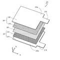
- FIG. 4 shows a current collector 103 with conductive layers on both sides of a resin layer.
- the current collector 103 includes a resin layer 10 having a first surface 10a and a second surface 10b opposite to the first surface 10a. A structure similar to that of the current collector 102 described above is formed on the first surface 10a of the resin layer 10 .
- the second surface 10b of the resin layer 10 also has a structure similar to that of the current collector 102 .
- the current collector 103 further comprises a conductive layer 20', a first intermediate layer 31', and a second intermediate layer 32'.
- the first intermediate layer 31' is located between the resin layer 10 and the conductive layer 20'.
- the second intermediate layer 32 ′ is positioned between the first intermediate layer 31 ′ and the resin layer 10 .
- the materials and thicknesses constituting the conductive layer 20', the first intermediate layer 31' and the second intermediate layer 32', the functions of these layers, etc. are described in the corresponding conductive layer 20, the first intermediate layer 31 and the second intermediate layer 31'. Same as layer 32 .
- the materials and thicknesses that make up the conductive layer 20′, the first intermediate layer 31′ and the second intermediate layer 32′ are different from those of the corresponding conductive layer 20, the first intermediate layer 31 and the second intermediate layer 32. It may be the same as the constituent material and thickness.
- the current collector 103 since the conductive layers 20 and 20' are provided on both sides of the resin layer 10, electrodes can be formed on both sides. Therefore, the proportion of the resin layer in the electricity storage device can be reduced, and the battery capacity per unit area can be increased.
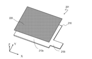
- FIG. 5 is an exploded perspective view of the electricity storage device electrode 201.
- the electricity storage device electrode 201 includes a current collector 210 and an active material layer 220 .
- Current collector 210 includes a first portion 210s and a second portion 210t, and active material layer 220 is disposed on first portion 210s.
- the second portion 210t is not provided with the active material layer 220 and functions as a tab for electrical connection to the outside.
- Active material layer 220 includes an active material that is oxidized and reduced during charging (or storage) and discharging.
- Current collector 210 supports active material layer 220 , supplies electrons to active material layer 220 , and receives electrons from active material layer 220 .
- the current collector 210 is the current collectors 101, 102, and 103 described in the first embodiment or the second embodiment. When current collector 103 is used, another active material layer not shown in FIG. .
- Active material layer 220 includes a positive electrode active material or a negative electrode active material that absorbs and releases lithium ions.
- the positive electrode active material includes, for example, a composite metal oxide containing lithium.
- the active material layer 220 may further contain at least one of a binder and a conductive aid.
- a binder Various known materials can be used for the binder. Binders in the active material layer 220 used for the positive electrode include polyvinylidene fluoride (PVDF), polytetrafluoroethylene (PTFE), tetrafluoroethylene-hexafluoropropylene copolymer (FEP), and tetrafluoroethylene-perfluoroalkyl vinyl ether.
- PVDF polyvinylidene fluoride
- PTFE polytetrafluoroethylene
- FEP tetrafluoroethylene-hexafluoropropylene copolymer
- tetrafluoroethylene-perfluoroalkyl vinyl ether tetrafluoroethylene-perfluoroalkyl vinyl ether.
- Fluorine such as copolymer (PFA), ethylene-tetrafluoroethylene copolymer (ETFE), polychlorotrifluoroethylene (PCTFE), ethylene-chlorotrifluoroethylene copolymer (ECTFE) and polyvinyl fluoride (PVF) Resin can be used.
- PFA copolymer
- ETFE ethylene-tetrafluoroethylene copolymer
- PCTFE polychlorotrifluoroethylene
- ECTFE ethylene-chlorotrifluoroethylene copolymer
- PVF polyvinyl fluoride
- a vinylidene fluoride-based fluorororubber may be used as the binder.
- vinylidene fluoride-hexafluoropropylene-based fluororubber VDF-HFP-based fluororubber
- vinylidene fluoride-hexafluoropropylene-tetrafluoroethylene-based fluororubber VDF-HFP-TFE-based fluororubber
- vinylidene fluoride- Pentafluoropropylene fluororubber VDF-PFP fluorubber
- vinylidene fluoride-pentafluoropropylene-tetrafluoroethylene fluororubber VDF-PFP-TFE fluorubber
- vinylidene fluoride-perfluoromethyl vinyl ether-tetra Fluoroethylene-based fluororubber VDF-PFMVE-TFE-based fluororubber
- Examples of conductive aids are carbon materials such as carbon powder and carbon nanotubes. Carbon black or the like can be applied to the carbon powder.
- Other examples of the conductive aid for the active material layer 220 used for the positive electrode are metal powders such as nickel, stainless steel and iron, and powders of conductive oxides such as ITO. Two or more of the above materials may be mixed and contained in the active material layer 220 .
- the negative electrode active material contains a carbon material.
- carbon materials include natural or artificial graphite, carbon nanotubes, non-graphitizable carbon, easily graphitizable carbon (soft carbon), low-temperature fired carbon, and the like.
- the negative electrode active material may contain materials other than the carbon material.
- alkali metals such as metallic lithium and alkaline earth metals, metals such as tin that can form compounds with metals such as lithium, silicon, silicon-carbon composites, amorphous compounds mainly composed of oxides (SiO x (0 ⁇ x ⁇ 2), tin dioxide, etc.), lithium titanate (Li 4 Ti 5 O 12 ), and other particles may be included.
- the binder and conductive aid of the active material layer 220 used for the negative electrode can be used in the same manner.
- Cellulose, styrene/butadiene rubber, ethylene/propylene rubber, polyimide, polyamideimide, acrylic resin, or the like may also be used as a binder for the negative electrode.
- the positive electrode and negative electrode for an electricity storage device can be manufactured by a known manufacturing method.
- the electricity storage device electrode of the present embodiment has high corrosion resistance to decomposition products of the electrolyte in the non-aqueous electrolyte. For this reason, even when the lithium ion secondary battery including the electricity storage device electrode of the present embodiment is used under conditions that facilitate decomposition of the electrolyte, for example, even when the lithium ion secondary battery is used at high temperatures, the battery characteristics due to deterioration of the current collector decrease in
- FIG. 6 is a schematic external view showing an example of the lithium ion secondary battery 301
- FIG. 7 is an exploded perspective view showing cells in the lithium ion secondary battery shown in FIG.
- a lithium ion secondary battery a pouch type or laminated type lithium ion secondary battery is exemplified.
- the illustrated lithium ion secondary battery is of a single layer type, but may be of a laminated type.
- the positive electrode, separator, and negative electrode that constitute the cell are stacked along the Z direction in the figure.
- a lithium ion secondary battery 301 includes a cell 310 , a pair of leads 311 connected to the cell 310 , an exterior body 313 covering the cell 310 , and an electrolyte 314 .
- the cell 310 includes an electricity storage device electrode 201, an electricity storage device electrode 201', and a separator 320 arranged therebetween.
- cell 310 is a single layer cell that includes a pair of electrodes.
- the power storage device electrode 201 and the power storage device electrode 201′ are the power storage device electrode 201 described in the third embodiment, one of which is a positive electrode containing a positive electrode active material, and the other is a negative electrode containing a negative electrode active material. It is configured.
- the separator 320 is an insulating porous material.
- Nonwoven fabrics, porous films, and the like can be used.
- the electrolyte 314 is further arranged in the space inside the exterior body 313 .
- the electrolyte 314 is a non-aqueous electrolyte containing lithium ions, such as a non-aqueous electrolytic solution containing lithium ions.
- a sealing material for example, a resin film such as polypropylene
- a resin film such as polypropylene
- a nonaqueous electrolytic solution containing a metal salt such as a lithium salt and an organic solvent can be used.
- Lithium salts include, for example, LiPF6 , LiClO4, LiBF4 , LiCF3SO3 , LiCF3CF2SO3 , LiC( CF3SO2 ) 3 , LiN( CF3SO2 ) 2 , LiN( CF3 CF2SO2 ) 2 , LiN( CF3SO2 )( C4F9SO2 ) , LiN( CF3CF2CO ) 2 , LiBOB and the like can be used.
- LiPF6 LiClO4, LiBF4 , LiCF3SO3 , LiCF3CF2SO3 , LiC( CF3SO2 ) 3 , LiN( CF3SO2 ) 2 , LiN( CF3 CF2SO2 ) 2 , LiN( CF3SO2 )( C4F9SO2 ) , Li
- cyclic carbonate and chain carbonate can be used.
- ethylene carbonate, propylene carbonate, butylene carbonate, dimethyl carbonate and the like can be used.
- the lithium ion secondary battery 301 can be manufactured, for example, by the following method. First, electrodes 201 and 201' are fabricated as described in the above embodiment. After that, the electrode 201 and the electrode 201 ′ are held so that the active material layers face each other with the separator 320 interposed therebetween, and inserted into the space of the exterior body 313 . Lithium ion secondary battery 301 is completed by arranging electrolyte 314 in the space of package 313 and sealing package 313 .
- the lithium-ion secondary battery 301 has high corrosion resistance against decomposition products of the electrolyte in the non-aqueous electrolyte. Therefore, even when the lithium ion secondary battery is used at high temperatures, deterioration of battery characteristics due to deterioration of the current collector is suppressed.
- Example A current collector of an example and a current collector of a reference example were produced and their properties were evaluated.
- a current collector 102 having the structure shown in FIG. 3 was produced.
- a polyethylene terephthalate resin having a thickness of 5 ⁇ m was used for the resin layer 10 .
- the first intermediate layer 31 and the second intermediate layer 32 were formed by a sputtering method using the metals or metal oxides shown in Tables 3 to 6 as targets. The thicknesses of the first intermediate layer 31 and the second intermediate layer 32 were adjusted by the deposition time and power.
- the Cu conductive layer 20 was formed separately into a seed layer 21 and a main layer 22 . After forming the seed layer 21 with a thickness of 50 nm, the main layer 22 with a thickness shown in Tables 3 to 6 was formed by electroplating.
- the conductive layers of Al and Cu--Ni were formed with the thicknesses shown in Tables 3 to 6 by a sputtering method.
- the molar ratio of metal to oxygen was controlled to be 1:1.
- a metal carbide was also used as the target.
- the composition ratio in the metal oxide was confirmed by composition analysis using X-ray photoelectron spectroscopy (XPS).
- the current collectors of Reference Examples 1 to 4 were produced without forming at least one of the first intermediate layer and the second intermediate layer.
- the (111) plane orientation index of the conductive layer was measured by the X-ray diffraction method, and obtained by the orientation index F according to the Lotgering method described above.
- the apparatus and measurement conditions used for the measurement are as follows.
- Measurement Method Out of Plane
- Examples 1 to 24 and Reference Examples 1 to 4 were held in an environment similar to that of a lithium ion secondary battery, and peeling of the conductive layer and corrosion of the conductive layer were evaluated. Specifically, an electrolytic solution of dimethyl carbonate containing LiPF 6 at a concentration of 1 mol % was prepared. Further, an electrolytic solution 1 was prepared by adding water to the electrolytic solution at a rate of 1000 ppm by mass. Similarly, electrolyte solution 2 was prepared with the amount of water to be added at a rate of 3000 ppm by mass, and electrolyte solution 3 was prepared by adjusting the amount of water to be added at a rate of 5000 ppm by mass.
- any one of electrolyte solutions 1 to 3 was placed in a container, the prepared current collector was immersed in the electrolyte solution in the container, the whole was sealed with a laminate film, and stored in a constant temperature bath at 85°C for 72 hours. After that, the current collector was taken out from the laminate film and washed with an organic solvent.
- Corrosion resistance was evaluated by observing the surface resistance of the conductive layer and an optical microscope.
- the surface resistance of the conductive layer was measured with a low resistance resistivity meter (trade name: Loresta GX MCP-T700, manufactured by Nitto Seiko Analytic Tech). Observation with an optical microscope was performed at a magnification of 100 to 200 times, arbitrary three observation areas were selected, and determination was made as to whether or not holes were formed in the selected areas.
- the surface resistance value of the conductive layer increases by 20% or more compared to before high-temperature storage, or if holes are found in the conductive layer by observation, it is determined to be unacceptable (POOR), and the increase in resistance value is 20%. % and no hole was found in the conductive layer, it was determined as GOOD.
- Peeling resistance was evaluated by two methods. The surface of the conductive layer of the current collector after high-temperature storage was rubbed with a cotton swab, and when a part of the conductive layer adhered to the cotton swab, it was determined that the conductive layer had separated from the resin layer, and it was determined to be unsatisfactory (POOR). In addition, an adhesive tape having an adhesive force of 4 N/cm was attached to the surface of the conductive layer of the current collector after high-temperature storage, and whether or not the conductive layer adhered was examined. When no peeling by the cotton swab was observed, but adhesion by the adhesive tape was observed, it was judged to be good (GOOD). When neither peeling with a cotton swab nor adhesion with an adhesive tape was observed, it was judged as excellent (EXCELLENT).
- Table 2 summarizes the produced current collector, the electrolyte used for storage, and the evaluation performed. Evaluation results are shown in Tables 3 to 6.
- the conductive layer when the thickness of the first intermediate layer is 1 nm or more and 120 nm or less, the conductive layer can obtain good corrosion resistance and peeling resistance. In particular, when the thickness of the first intermediate layer is 2 nm or more and 100 nm or less, the conductive layer has excellent corrosion resistance and peeling resistance. Further, from Tables 3 and 4, it can be seen that if D1/D2, which is the ratio of the first intermediate layer to the second intermediate layer, satisfies D1/D2 ⁇ 10, a current collector excellent in both peel resistance and corrosion resistance can be obtained. It is understood that Furthermore, it can be seen that when D1/D2 satisfies 2 ⁇ D1/D2 ⁇ 10, the current collector is more excellent in peel resistance and corrosion resistance.
- the surface energy of Ag which is the metal of the first intermediate layer
- the energy of Cu which is the metal of the conductive layer
- the surface energy of the metal of the first intermediate layer is higher than the energy of the metal of the conductive layer.
- the (111) plane orientation index is as small as 0.25 in the current collector of Example 16, and the current collectors of Examples 14, 15, and 17 to 20, which are examples other than Example 16, has a large value of 0.65 or more. This is considered to indicate that the magnitude relationship of the surface energy of the metal between the first intermediate layer and the conductive layer affects the ease of (111) plane orientation, as described above.
- the metals constituting the first intermediate layer are various such as Cr, Mo, Co, Ni—Cr, and W.
- the (111) plane orientation index is large in any of the current collectors. This is considered to indicate that the lattice constant of the crystal of the metal forming the first intermediate layer and the crystallinity of the first intermediate layer have little effect on the (111) plane orientation index.
- the current collectors of Examples 14, 15, and 17 to 20 have improved corrosion resistance of the conductive layers. This is considered to indicate that there is a correlation between the value of the (111) plane orientation index of the conductive layer and the corrosion resistance.
- the conductive layer is effectively conductive. It is thought that the orientation of the (111) plane of the layer can be enhanced, and the corrosion resistance can be improved.
- the current collector of the present embodiment has corrosion resistance and peeling resistance against decomposition products of the electrolyte in the non-aqueous electrolyte by including the first intermediate layer and the second intermediate layer. was found to be able to increase
- the power storage device electrodes according to the embodiments of the present disclosure are useful as power sources for various electronic devices, electric motors, and the like.
- Power storage devices according to embodiments of the present disclosure include, for example, power sources for vehicles typified by bicycles and passenger cars, power sources for communication devices typified by smartphones, power sources for various sensors, unmanned eXtended vehicles ( UxV)) power supply.
- UxV unmanned eXtended vehicles
Landscapes
- Chemical & Material Sciences (AREA)
- Engineering & Computer Science (AREA)
- Materials Engineering (AREA)
- Chemical Kinetics & Catalysis (AREA)
- Electrochemistry (AREA)
- General Chemical & Material Sciences (AREA)
- Cell Electrode Carriers And Collectors (AREA)
Abstract
集電体は、樹脂層と、導電層と、前記樹脂層と前記導電層との間に位置する第1中間層と、前記第1中間層と、前記樹脂層との間に位置する第2中間層と、を備え、前記第1中間層は金属を主成分として含み、前記第2中間層は金属酸化物を主成分として含む。
Description
本開示は、集電体、蓄電デバイス用電極、および、リチウムイオン二次電池に関する。
二次電池の集電体として、樹脂フィルムの片面または両面に導電層を形成した複合材を用いることが提案されている。特許文献1は、そのような複合材を集電体に適用した二次電池用の集電体を開示している。
リチウムイオン二次電池のような非水電解液を備えた蓄電デバイスでは、非水電解液の分解生成物によって集電体が劣化することが知られている。上述した複合材の集電体をリチウムイオン二次電池のような非水電解液を備えた蓄電デバイスに用いる場合も、非水電解液の分解生成物による影響を考慮することが好ましい。本開示の一実施形態は、電解質の分解生成物による劣化が抑制された集電体、蓄電デバイス用電極およびリチウムイオン二次電池を提供する。
本開示の一実施形態にかかる集電体は、樹脂層と、導電層と、前記樹脂層と前記導電層との間に位置する第1中間層と、前記第1中間層と、前記樹脂層との間に位置する第2中間層と、を備え、前記第1中間層は金属を主成分として含み、前記第2中間層は金属酸化物を主成分として含む。
本開示の一実施形態によると、電解質の分解生成物による劣化が抑制された集電体が提供される。
樹脂フィルムに導電層が形成された集電体は、構造および厚さの点で、従来、集電体として単体で用いられる金属箔とは異なっている。特に、集電体が樹脂フィルムと導電層との複合体であり、導電層が従来の集電体に用いられる金属箔よりも薄いことが、従来の集電体とは異なる。
リチウムイオン二次電池は、一般にフッ素原子を含むアニオンを電解質として含んでいる。このようなリチウムイオン二次電池を高温の環境下で充放電させる場合、フッ素原子を含むアニオンが分解し、分解生成物としてフッ素イオン、つまり、フッ酸が生じる。本願発明者は、非水電解液の分解生成物による、樹脂フィルムに導電層が形成された集電体の劣化を抑制すること、具体的には、導電層の溶解・欠損、および、樹脂フィルムからの導電層の剥離の少なくとも一方を抑制することによって、充放電特性を維持し得る集電体、蓄電デバイス用電極およびリチウムイオン二次電池を想到した。
以下、図面を参照しながら、本開示の集電体、蓄電デバイス用電極およびリチウムイオン二次電池の実施形態を説明する。以下の説明で提示される数値、形状、材料、ステップ、そのステップの順序などは、あくまでも一例であって、技術的に矛盾が生じない限りにおいて種々の改変が可能である。また、以下に説明する各実施形態も、あくまでも例示であり、技術的に矛盾が生じない限りにおいて種々の組み合わせが可能である。
本開示の図面に表された部材の厚さ、寸法、形状等は、説明の便宜のために誇張されていることがある。また、本開示の図面では、過度の複雑さを避けるために、一部の部材を取り出して図示したり、一部の要素の図示を省略したりすることがある。そのため、本開示の図面に表された部材のそれぞれの寸法および部材間の配置は、実際のデバイスにおける部材のそれぞれの寸法および部材間の配置を反映しないことがある。本開示における「垂直」および「直交」は、2つの直線、辺、面等が厳密に90°の角度をなしていることに限られず、90°から±5°程度の範囲にある場合を含む。また、「平行」は、2つの直線、辺、面等が0°から±5°程度の範囲にある場合を含む。
本明細書において、「セル」の用語は、少なくとも一対の正極および負極が一体的に組み立てられた構造を指す。本明細書の「電池」の用語は、互いに電気的に接続された1以上の「セル」を有する、電池モジュール、電池パック等の種々の形態を包括する用語として用いられる。
(第1の実施形態)
図1は、本実施形態の集電体の一例を示す模式的な断面図である。本実施形態の集電体はリチウムイオン二次電池などの蓄電デバイスの正極および負極のいずれの電極の集電体としても用いることができる。集電体101は、樹脂層10と、導電層20と、樹脂層と導電層20との間に位置する第1中間層31とを備える。
図1は、本実施形態の集電体の一例を示す模式的な断面図である。本実施形態の集電体はリチウムイオン二次電池などの蓄電デバイスの正極および負極のいずれの電極の集電体としても用いることができる。集電体101は、樹脂層10と、導電層20と、樹脂層と導電層20との間に位置する第1中間層31とを備える。
樹脂層10は、集電体101において、導電層20の支持体として機能する。また、樹脂層10は、導電層20よりも小さい密度を有することによって、蓄電デバイスを構成した場合において、単位重量当たりの充電容量を高めることに寄与し得る。
樹脂層10は電気絶縁性を備えており、樹脂を含む。樹脂層10は熱可塑性を備えていてもよい。樹脂層10は、具体的には、ポリエチレンテレフタレート(PET)、ポリプロピレン(PP)、ポリアミド(PA)、ポリイミド(PI)、ポリエチレン(PE)、ポリスチレン(PS)、フェノール樹脂(PF)、エポキシ樹脂(EP)のいずれか1種を少なくとも含んでいてもよい。樹脂層10は、単層であってもよいし、2以上の複数の層を積層することによって構成されていてもよい。この場合、複数の層のうち、少なくとも1層は、異なる樹脂を含んでいてもよい。
樹脂層10の厚さは、例えば、3μm以上12μm以下である。樹脂層10の厚さは3μm以上6μm以下であってもよい。樹脂層10の厚さが3μm以上であることによって、支持体として十分な強度が得られる。また、樹脂層10の厚さが12μm以下であることによって、集電体101全体の厚さを小さくできる。このため、複数の電極対を積層した積層型リチウムイオン二次電池を構成した場合、エネルギーの蓄積に寄与しない部分の割合を少なくでき、エネルギー密度を大きくし得る。樹脂層10の厚さが6μm以下であれば、より集電体101全体の厚さを小さくし、積層型リチウムイオン二次電池のエネルギー密度を大きくすることができる。
集電体101は、樹脂層10と第1中間層31との間に位置するアンダーコート層をさらに備えていてもよい。アンダーコート層は、樹脂層10と第1中間層31との接合強度を高めたり、第1中間層31にピンホールが形成されるのを抑制したりするために設けられ得る。例えば、アンダーコート層は、アクリル樹脂、ポリオレフィン樹脂等の有機材料から形成された層、または、スパッタリングにより形成された、金属を含有する層であってもよい。
第1中間層31は、導電層20の結晶配向性を制御する。具体的には、第1中間層31は、第1中間層31上に形成される導電層20がより緻密な結晶構造を有するように導電層20の結晶配向性を制御する。第1中間層31は、金属を主成分として含み、第1中間層31に含まれる金属の表面エネルギーは、導電層20に主成分として含まれる金属の表面エネルギーよりも大きい。以下において詳述するように、この関係を満たすことによって、導電層20は、(111)配向しやすくなる。主成分とは、部材が1または複数の成分を含む場合において、モルパーセントで表した含有の割合が最も多い成分をいう。
第1中間層31の厚さD1は、例えば、1nm以上120nm以下である。第1中間層31の厚さD1が1nm以上であれば、連続した膜を形成でき、形成する導電層20全体の配向性を制御しやすくなる。第1中間層31の厚さD1が120nm以下であることによって、第1中間層31の形成に要する時間が長くなりすぎず、第1中間層31の形成時の条件によるダメージ、例えば、熱やプラズマが樹脂層10に与える影響が小さくなり、樹脂層10の劣化が抑制できる。第1中間層31の厚さは、2nm以上100nm以下であってもよい。
第1中間層31は、例えば、Ni、Cr、Co、Ti、Zr、Nb、Hf、TaおよびWからなる群から選ばれる少なくとも1種の金属を含むことができる。これらの金属のうち、導電層20の金属との間で、上述した表面エネルギーの関係を満たすものを選択することができる。導電層20がCuからなる場合、第1中間層31は、例えば、Ni、Cr、Ni-Cr合金、Co、Wとすることができる。導電層20がAlからなる場合、第1中間層31は、例えば、Ni、Crとすることができる。第1中間層31は、真空蒸着法、スパッタ法など半導体装置の製造に用いられる公知の薄膜形成技術を用いて形成することができる。
導電層20は、集電体101における主たる電流路であり、正極活物質または負極活物質と集電体と接続される端子等との間で電子の授受を行う。導電層20は、金属を主成分として含み、第1中間層31の働きによって、(111)配向性を有している。(111)配向性を備えるという観点から、導電層20は第1中間層31と接していてもよい。
一般に、金属層の(111)面は、(100)、(110)等に比べて、表面原子密度が大きいため、耐食性に優れる。このため、導電層20は、リチウムイオン二次電池等の非水電解液において、電解質の分解生成物に対する高い耐腐食性を備えている。
導電層20において、(111)面の配向性は高くてもよい。具体的には、樹脂層10の垂直方向に対するロットゲーリング法による導電層20の(111)面の配向指数を0.3以上とすることができる。配向指数は、例えば、0.7以上とすることができる。配向指数については以下において詳述する。
導電層20の厚さは、例えば、0.3μm以上2μm以下である。導電層20の厚さが0.3μm以上であることにより、導電層20の抵抗を小さくできる。例えば、蓄電デバイスを作製した場合に集電体における抵抗によるエネルギーロスを小さくできる。また、導電層20の厚さが2μm以下であることにより、相対的に樹脂層10に対する導電層20の割合が小さくなり、樹脂層10を用いて集電体の重量を軽減させるというメリットが得られやすくなる。導電層20の厚さは、0.5μm以上1.2μm以下であってもよい。
導電層20は、例えば、Al、Ag、Cu、NiおよびNi-Cu合金からなる群から選ばれる1種の金属を含むことができる。集電体101が正極に用いられる場合には、導電層20はAlを含んでいてもよい。集電体101が負極に用いられる場合には、導電層20はAg、Cu、NiおよびNi-Cu合金からなる群から選ばれる1種の金属を含んでいてもよい。
本実施形態では、導電層20は、シード層21と、主層22とを含む。シード層21および主層22はそれぞれ金属を主成分とし、同じ金属によって構成されていてもよい。
シード層21は、例えば、スパッタ法や真空蒸着法によって形成され、主層22は、めっき法によって形成される。これは、導電層20が比較的厚く、導電層20全体をスパッタ法や真空蒸着法によって形成する場合、形成時間が長くなり、生産性が低下することおよび導電層20の形成時に樹脂層10に与えるダメージが大きくなるのを避けるためである。ただし、導電層20はシード層21を含んでいなくてもよい。例えば、第1中間層31を、めっきを行うための導電層として用いてもよい。
導電層20がシード層21と、主層22とを含む場合、第1中間層31と接するシード層21は、第1中間層31の働きによって、(111)配向性を備える。主層22は、シード層21の配向性に従い、(111)配向性を備える。
次に、第1中間層31による導電層20の配向性制御について説明する。前述したように非水電解液中に含まれる電解質の分解生成物による腐食を抑制するためには、緻密な配向面である(111)面の配向性が高い導電層を集電体に用いることが考えられる。本願発明者は種々の金属からなる下地層を形成し、その上に形成されるCu層の配向性を調べた。図2は、下地層上にCu層を形成した場合における、下地層を構成する金属の表面エネルギーと、Cu層の(111)面配向指数との関係を示す。試料は、基板上にAl、Ag-Pd-Cu、Cu、Ni-Cr、Tiからなる下地層を形成し、その上にCu層を形成している。下地層の厚さは、10nm、Cu層の厚さは、50nm~60nmであり、スパッタ法により形成している。
(111)面配向指数はロットゲーリング法による配向指数Fである。ロットゲーリング法による配向指数の最大値は1である。配向指数が1であるときは完全に配向していることを示し、配向指数が0であるときは配向していないことを示す。配向指数Fは、評価すべき層(膜)のX線回折測定によって得られるX線回折ピークの強度を用いて、以下の式によって求められる。
F=(ρ-ρ0)/(1-ρ0)
ρ0=ΣI0(111)/ΣI0(hkl)
ρ=ΣI(111)/ΣI(hkl)
F=(ρ-ρ0)/(1-ρ0)
ρ0=ΣI0(111)/ΣI0(hkl)
ρ=ΣI(111)/ΣI(hkl)
I0(111)は、無配向のCu粉のX線回折測定によって得られた(111)面のX線回折ピークの強度を示す。I0(hkl)は、無配向のCu膜のX線回折測定によって得られた全回折ピークの強度を示す。また、無配向のCu膜とは、X線回折ピークの強度パターンが、JCPDS(Joint Committee on Powder Diffraction Standards)に掲載されている銅の標準試料におけるX線回折ピークの強度パターンに近い強度パターンを示すCu膜であることを意味する。
I(111)は、評価すべき層(膜)のX線回折測定によって得られた(111)面のX線回折ピークの強度を示す。I(hkl)は、評価すべき層(膜)のX線回折測定によって得られた全回折ピークの強度を示す。
金属の表面エネルギーは、非特許文献 L.Vitos、A.V.Ruban、H.L.Skriver、J.Kollar、“The surface energy of metals”、Surface Science、Elsevier、1998、Vol.411、Pages 186-202、に記載された実測値を用いた。表1に種々の金属の表面エネルギーの文献値を示す。合金については、含有比率に基づき表1の値から計算した。金属の表面エネルギーは、正確に実測することが困難であり、文献によって金属の表面エネルギーの値は、10%程度異なる。表1に示す値は、金属の表面エネルギーの一例である。
図2に示すように、下地層の上に形成するCu層の(111)面配向指数は、下地層の金属の種類によって異なり、下地層を構成する金属の表面エネルギーと、Cu層の(111)面配向指数との間には相関があると考えられる。下地層を構成する金属の表面エネルギーが高いほど、Cu層の(111)面配向指数も大きくなっている。
一方、金属の表面エネルギーには面方位の依存性があることが知られており、FCC構造をとる金属においては、表面エネルギーは、(110)>(100)>(111)の関係がある。
これらのことから、第1中間層31の金属の表面エネルギーが導電層20の金属の表面エネルギーよりも大きい場合には、第1中間層31上への導電層20の形成は、エネルギー的に有利な状態変換であるため、第1中間層31が露出した状態から、最もエネルギー差が大きい状態、つまり、導電層20の(111)面が形成される状態へ第1中間層31の金属の原子が選択的に配列されると考えられる。
図2より、導電層20がCuを主成分とする場合、第1中間層31の表面エネルギーが、1.5J/m2以上であれば、導電層20が、0.7程度以上の(111)面配向指数を示すと期待される。

このように本実施形態の集電体によれば、第1中間層31が、金属を主成分として含み、第1中間層31に含まれる金属の表面エネルギーが、導電層20に主成分として含まれる金属の表面エネルギーよりも大きいことによって、(111)配向性が高い導電層20が形成されやすくなる。したがって、導電層20は、リチウムイオン二次電池等において、電解質の分解生成物に対する高い耐腐食性を備えている。
(第2の実施形態)
図3は、本実施形態の集電体の一例を示す模式的な断面図である。本実施形態の集電体102は、樹脂層10と、導電層20と、第1中間層31と、第2中間層32とを備える。第1中間層31は、樹脂層10と、導電層20との間に位置している。第2中間層32は、第1中間層31と、樹脂層10との間に位置している。集電体102は、さらに、第2中間層32を備えている点で、第1の実施形態の集電体101と異なる。樹脂層10、導電層20および第1中間層31を構成する材料および厚さ、これらの層の機能等については、第1の実施形態で説明した通りである。
図3は、本実施形態の集電体の一例を示す模式的な断面図である。本実施形態の集電体102は、樹脂層10と、導電層20と、第1中間層31と、第2中間層32とを備える。第1中間層31は、樹脂層10と、導電層20との間に位置している。第2中間層32は、第1中間層31と、樹脂層10との間に位置している。集電体102は、さらに、第2中間層32を備えている点で、第1の実施形態の集電体101と異なる。樹脂層10、導電層20および第1中間層31を構成する材料および厚さ、これらの層の機能等については、第1の実施形態で説明した通りである。
第2中間層32は、樹脂層10と樹脂層10上に形成される層との密着性を高める。このために、第2中間層32は、金属酸化物を主成分として含んでいる。第2中間層32は、樹脂層10と接していてもよい。第2中間層32が金属酸化物を主成分として含むことによって、金属を主成分とする導電層20あるいは第1中間層31が樹脂層10と接する場合に比べて、樹脂層10との密着性が高められる。
第2中間層32の厚さD2は、例えば、0.5nm以上20nm以下である。第2中間層32の厚さD2が0.5nm以上であることによって、連続した第2中間層32が形成され、密着性向上の効果が得られやすい。第2中間層32の厚さが20nm以下であることによって、第2中間層32の形成に要する時間を短くすることができ、第2中間層32の形成時の条件によるダメージ、例えば、熱やプラズマが樹脂層10に与える影響を小さくして、樹脂層10の劣化を抑制し得る。第2中間層32の厚さは、1nm以上であってもよく、2nm以上であってもよい。また、第2中間層32の厚さは、10nm以下であってもよい。
第1中間層31の厚さD1および第2中間層32の厚さD2は、D1/D2≦10の関係を満たしていてもよい。D1/D2≦10であることによって、第1中間層31が厚くなり過ぎ、第2中間層32に大きな応力がかかることによって第2中間層32と樹脂層10との密着性が低下することが抑制されると考えられる。D1/D2は、2≦D1/D2≦10の関係を満たしていてもよい。
第2中間層32は、Ni、Cr、Co、Ti、Zr、Nb、Hf、TaおよびWからなる群から選ばれる少なくとも1種の金属の酸化物を含んでいてもよい。これらの金属酸化物は、不働態となり、酸化が内部まで進行しにくい。つまり、第2中間層32自体が、非水電解液中の電解質の分解生成物に対して難溶である。このため、第2中間層32が樹脂層10との界面等で溶解することが抑制され、高い密着性を長期間維持し得る。第2中間層32は、例えば、金属酸化物をターゲットに用いるスパッタ法や、金属をターゲットとし、酸素を含む雰囲気下でスパッタ法により形成することができる。
第2中間層32に含まれる金属酸化物中の酸素の割合は、モル比で、金属元素1に対して0.3以上であってもよい。つまり、金属酸化物は、下記組成式で示されてもよい。
MOx (x≧0.3)
MOx (x≧0.3)
ここで、Mは、Ni、Cr、Co、Ti、Zr、Nb、Hf、TaおよびWからなる群から選ばれる少なくとも1種である。
xが0.3以上であることによって、第2中間層32に極性が生じ、樹脂層10との間で分子間力が働きやすくなることによって、密着性が高まる。xは整数に限られない。xの上限は、金属がとり得る安定した酸化状態のうち最も大きい価数に依存する。
第2中間層32は、さらに金属炭化物を含んでいてもよい。Ni、Cr、Co、Ti、Zr、Nb、Hf、TaおよびWからなる群から選ばれる少なくとも1種の金属の炭化物を含むことによって、樹脂層10との密着性をさらに高めることができる。
また、第2中間層32に含まれる金属酸化物を構成する元素は、第1中間層31に含まれる金属と同じ元素であってもよい。この場合、例えば、第2中間層32と、第1中間層31とを同じ金属のターゲットを用いたスパッタ法によって連続的に形成することが可能であり、第2中間層32と第1中間層31との密着性も高めることが可能である。
本実施形態の集電体102によれば、金属酸化物を含む第2中間層32を備えることによって、導電層と樹脂層とが直接接する場合よりも導電層と樹脂層との密着性を高めることができる。また、金属を含む第1中間層31を含むことによって、第2中間層32だけの場合と異なり、導電層20が金属酸化物ではなく金属を主成分とする第1中間層31と接する。このため、導電層20を形成する際に導電層20の結晶性を高めることができ、導電層20の非水電解液中の電解質の分解生成物に対する耐腐食性を高めることができる。
また、第1中間層31に含まれる金属の表面エネルギーが、導電層20に主成分として含まれる金属の表面エネルギーよりも大きいことによって、導電層20の(111)配向性が高まる。したがって、導電層20は、リチウムイオン二次電池等の非水電解液において、生成し得る電解質の分解生成物に対する高い耐腐食性を備える。
なお、図3を参照して説明した集電体102は、樹脂層10の片面にのみ導電層20を備えていたが、両面に導電層20を備えていてもよい。図4は、樹脂層の両面に導電層を備えた集電体103を示す。集電体103は、第1面10aと第1面10aと反対側に位置する第2面10bとを有する樹脂層10を備えている。樹脂層10の第1面10aには上述した集電体102と同様の構造が形成されている。
一方、樹脂層10の第2面10bにも集電体102と同様の構造が形成されている。具体的には、集電体103は、導電層20’と、第1中間層31’と、第2中間層32’とをさらに備える。第1中間層31’は、樹脂層10と、導電層20’との間に位置している。第2中間層32’は、第1中間層31’と、樹脂層10との間に位置している。導電層20’、第1中間層31’および第2中間層32’を構成する材料および厚さ、これらの層の機能等については、対応する導電層20、第1中間層31および第2中間層32と同じである。応力の観点では、導電層20’、第1中間層31’および第2中間層32’を構成する材料および厚さは、対応する導電層20、第1中間層31および第2中間層32を構成する材料および厚さと同じであってもよい。
集電体103によれば、樹脂層10の両面に導電層20、20’を備えるため、両面に電極を形成することができる。よって、蓄電デバイスにおける樹脂層が占める割合を小さくして、単位面積当たりの電池容量を高めることができる。
(第3の実施形態)
蓄電デバイス用電極の実施形態を説明する。本実施形態の蓄電デバイス用電極は、蓄電デバイスの正極にも負極にも用いることができる。図5は、蓄電デバイス用電極201の分解斜視図である。蓄電デバイス用電極201は、集電体210と、活物質層220とを備える。集電体210は、第1部分210sと第2部分210tとを含み、第1部分210sに活物質層220が配置されている。第2部分210tには活物質層220は設けられておらず、外部への電気的接続のためのタブとして機能する。活物質層220は、充電(または蓄電)および放電に伴って酸化還元される活物質を含む。集電体210は、活物質層220を支持し、活物質層220へ電子を供給し、活物質層220から電子を受け取る。
蓄電デバイス用電極の実施形態を説明する。本実施形態の蓄電デバイス用電極は、蓄電デバイスの正極にも負極にも用いることができる。図5は、蓄電デバイス用電極201の分解斜視図である。蓄電デバイス用電極201は、集電体210と、活物質層220とを備える。集電体210は、第1部分210sと第2部分210tとを含み、第1部分210sに活物質層220が配置されている。第2部分210tには活物質層220は設けられておらず、外部への電気的接続のためのタブとして機能する。活物質層220は、充電(または蓄電)および放電に伴って酸化還元される活物質を含む。集電体210は、活物質層220を支持し、活物質層220へ電子を供給し、活物質層220から電子を受け取る。
集電体210は、第1の実施形態または第2の実施形態で説明した集電体101、102、103である。集電体103を用いる場合には、図5には示していない他の活物質層を集電体210の裏面側(活物質層220が配置されていない側)の第1部分210sに配置する。
活物質層220は、リチウムイオンを吸蔵および放出する正極活物質または負極活物質を含む。正極活物質は、例えば、リチウムを含有する複合金属酸化物を含む。リチウムを含有する複合金属酸化物として、コバルト酸リチウム(LiCoO2)、ニッケル酸リチウム(LiNiO2)、マンガン酸リチウム(LiMnO2)、リチウムマンガンスピネル(LiMn2O4)、リチウムバナジウム化合物(LiV2O5)、オリビン型LiMPO4(ただし、Mは、Co、Ni、Mn、Fe、Mg、Nb、Ti、Al、Zrからなる群より選ばれる1種類以上の元素またはバナジウム酸化物)、チタン酸リチウム(Li4Ti5O12)、一般式:LiNixCoyMnzMaO2(x+y+z+a=1、0≦x<1、0≦y<1、0≦z<1、0≦a<1、上記一般式中のMは、Al、Mg、Nb、Ti、Cu、Zn、Crからなる群より選ばれる1種類以上の元素)で表される複合金属酸化物、および、一般式:LiNixCoyAlzO2(0.9<x+y+z<1.1)で表される複合金属酸化物等を挙げることができる。正極活物質は、リチウムイオンを吸蔵および放出可能な材料として、ポリアセチレン、ポリアニリン、ポリピロール、ポリチオフェン、ポリアセン等を含有していてもよい。
活物質層220は、さらにバインダーおよび導電助剤の少なくとも一方を含んでいてもよい。バインダーには、公知の種々の材料を用いることができる。正極に用いる活物質層220中のバインダーとしては、ポリフッ化ビニリデン(PVDF)、ポリテトラフルオロエチレン(PTFE)、テトラフルオロエチレン-ヘキサフルオロプロピレン共重合体(FEP)、テトラフルオロエチレン-パーフルオロアルキルビニルエーテル共重合体(PFA)、エチレン-テトラフルオロエチレン共重合体(ETFE)、ポリクロロトリフルオロエチレン(PCTFE)、エチレン-クロロトリフルオロエチレン共重合体(ECTFE)およびポリフッ化ビニル(PVF)等のフッ素樹脂を用いることができる。
バインダーとして、ビニリデンフルオライド系フッ素ゴムを用いてもよい。例えば、ビニリデンフルオライド-ヘキサフルオロプロピレン系フッ素ゴム(VDF-HFP系フッ素ゴム)、ビニリデンフルオライド-ヘキサフルオロプロピレン-テトラフルオロエチレン系フッ素ゴム(VDF-HFP-TFE系フッ素ゴム)、ビニリデンフルオライド-ペンタフルオロプロピレン系フッ素ゴム(VDF-PFP系フッ素ゴム)、ビニリデンフルオライド-ペンタフルオロプロピレン-テトラフルオロエチレン系フッ素ゴム(VDF-PFP-TFE系フッ素ゴム)、ビニリデンフルオライド-パーフルオロメチルビニルエーテル-テトラフルオロエチレン系フッ素ゴム(VDF-PFMVE-TFE系フッ素ゴム)、ビニリデンフルオライド-クロロトリフルオロエチレン系フッ素ゴム(VDF-CTFE系フッ素ゴム)等を正極に用いる活物質層220のバインダーに適用してもよい。
導電助剤の例は、カーボン粉末、カーボンナノチューブ等の炭素材料である。カーボン粉末には、カーボンブラック等を適用できる。正極に用いる活物質層220の導電助剤の他の例は、ニッケル、ステンレス、鉄等の金属粉末、および、ITO等の導電性酸化物の粉末である。上述した材料の2種以上を混合して活物質層220に含有させてもよい。
負極活物質は炭素材料を含む。炭素材料の例としては、例えば、天然または人造の黒鉛、カーボンナノチューブ、難黒鉛化性炭素、易黒鉛化性炭素(ソフトカーボン)、低温度焼成炭素等が挙げられる。負極活物質は炭素材料以外の材料を含んでいてもよい。例えば、金属リチウム等のアルカリ金属およびアルカリ土類金属、リチウム等の金属と化合物を形成できる、スズ等の金属またはシリコン、シリコン・カーボン複合材、酸化物を主体とする非晶質の化合物(SiOx(0<x<2)、二酸化スズ等)、チタン酸リチウム(Li4Ti5O12)等の粒子を含んでいてもよい。
負極に用いられる活物質層220のバインダーおよび導電助剤には、上述したバインダーおよび導電助剤を同様に用いることができる。また、負極用のバインダーとして、セルロース、スチレン・ブタジエンゴム、エチレン・プロピレンゴム、ポリイミド、ポリアミドイミド、アクリル樹脂等を用いてもよい。
正極用および負極用の蓄電デバイス用電極は、公知の製造方法によって製造することができる。
本実施形態の蓄電デバイス用電極は、非水電解液中の電解質の分解生成物に対する高い耐腐食性を備えている。このため、本実施形態の蓄電デバイス用電極を含むリチウムイオン二次電池が、電解質の分解しやすい条件、例えば、高温でリチウムイオン二次電池が使用される場合でも集電体の劣化による電池特性の低下が抑制される。
(第4の実施形態)
リチウムイオン二次電池の実施形態を説明する。
リチウムイオン二次電池の実施形態を説明する。
図6は、リチウムイオン二次電池301の一例を示す模式的な外観図であり、図7は、図6に示すリチウムイオン二次電池におけるセルを取り出して示す分解斜視図である。ここでは、リチウムイオン二次電池として、パウチ型あるいはラミネート型と呼ばれるリチウムイオン二次電池を例示する。図示するリチウムイオン二次電池は、単層型であるが、積層型であってもよい。図示する例において、セルを構成する正極、セパレータおよび負極は、図のZ方向に沿って積層されている。
リチウムイオン二次電池301は、セル310と、セル310に接続された一対のリード311と、セル310を覆う外装体313と、電解質314とを備える。
セル310は、蓄電デバイス用電極201と、蓄電デバイス用電極201’と、これらの間に配置されたセパレータ320とを含む。図示する例では、セル310は、一対の電極を含む単層セルである。
蓄電デバイス用電極201と、蓄電デバイス用電極201’とは第3の実施形態で説明した蓄電デバイス用電極201であり、一方が正極活物質を含む正極として、他方が負極活物質を含む負極として構成されている。
セパレータ320は、絶縁性の多孔質材である。例えば、ポリエチレン、ポリプロピレン等のポリオレフィンの単層フィルムもしくは積層フィルム、または、セルロース、ポリエステル、ポリアクリロニトリル、ポリイミド、ポリアミド(例えば芳香族ポリアミド)、ポリエチレンおよびポリプロピレンからなる群より選択される少なくとも1種の繊維の不織布、多孔質フィルムなどを用いることができる。
外装体313の内側の空間には、電解質314がさらに配置される。電解質314は、リチウムイオンを含む非水電解質であり、例えば、リチウムイオンを含む非水電解液である。電解質314に非水電解液を適用した場合、典型的には、外装体313とリード311との間に、非水電解液の漏出を防止するための封止材(例えば、ポリプロピレン等の樹脂フィルム、図6において不図示)が配置される。
電解質314としては、例えば、リチウム塩等の金属塩および有機溶媒を含有する非水電解液を用いることができる。リチウム塩には、例えば、LiPF6、LiClO4、LiBF4、LiCF3SO3、LiCF3CF2SO3、LiC(CF3SO2)3、LiN(CF3SO2)2、LiN(CF3CF2SO2)2、LiN(CF3SO2)(C4F9SO2)、LiN(CF3CF2CO)2、LiBOB等を使用できる。これらのリチウム塩の1種を単独で使用してもよく、2種以上を混合させてもよい。
電解質314の溶媒には、例えば、環状カーボネートおよび鎖状カーボネートを用いることができる。具体的には、エチレンカーボネート、プロピレンカーボネート、ブチレンカーボネート、ジメチルカールボネート等を用いることができる。
リチウムイオン二次電池301は、例えば以下の方法によって製造できる。まず、上記実施形態で説明したように電極201、201’を作製する。その後、セパレータ320を介して活物質層同士が対向するように電極201および電極201’を保持し、外装体313の空間に挿入する。電解質314を外装体313の空間に配置し、外装体313を封止することによって、リチウムイオン二次電池301が完成する。
リチウムイオン二次電池301によれば、非水電解液中の電解質の分解生成物に対する高い耐腐食性を備えている。このため、高温でリチウムイオン二次電池が使用される場合でも集電体の劣化による電池特性の低下が抑制される。
(実施例)
実施例の集電体および参考例の集電体を作製し、特性を評価した。
実施例の集電体および参考例の集電体を作製し、特性を評価した。
[試料の作製]
実施例1から実施例24および参考例1から参考例4の集電体を以下の方法により作製した。
実施例1から実施例24および参考例1から参考例4の集電体を以下の方法により作製した。
図3に示す構造を備えた集電体102を作製した。樹脂層10には、厚さ5μmのポリエチレンテレフタレート樹脂を用いた。第1中間層31、第2中間層32は、表3から表6に示す金属または金属酸化物をターゲットに用いたスパッタ法により形成した。第1中間層31および第2中間層32の厚さは、堆積時間及び出力によって調節した。Cuの導電層20は、シード層21および主層22に分けて形成した。厚さ50nmのシード層21を形成した後、表3から表6に示す厚さの主層22を電解めっきによって形成した。AlおよびCu-Niの導電層は、表3から表6に示す厚さで、スパッタ法により形成した。
実施例14から実施例20および実施例21、23における、第2中間層については、金属と酸素との割合が、モル比で1:1となるように制御した。実施例22、24については、さらに金属炭化物をターゲットとして用いた。金属酸化物中の組成比はX線光電子分光法(XPS)による組成分析によって確認した。
参考例1から参考例4の集電体は、表3に示すように、第1中間層および、第2中間層の少なくとも一方を形成せずに作製した。
[評価]
導電層の(111)面配向指数は、X線回折法により測定を行い、上述したロットゲーリング法による配向指数Fによって求めた。測定に使用した装置および測定条件は以下の通りである。
装置名:PANalytical XPert PRO
線源:CuKα線
加速電圧:40kV
電流:45mA
スキャンスピード:6deg./min.
サンプリング幅:0.02deg.
測定方法:アウトオブプレーン
導電層の(111)面配向指数は、X線回折法により測定を行い、上述したロットゲーリング法による配向指数Fによって求めた。測定に使用した装置および測定条件は以下の通りである。
装置名:PANalytical XPert PRO
線源:CuKα線
加速電圧:40kV
電流:45mA
スキャンスピード:6deg./min.
サンプリング幅:0.02deg.
測定方法:アウトオブプレーン
実施例1から実施例24および参考例1から参考例4の集電体をリチウムイオン二次電池と類似した環境で保持し、導電層の剥離および導電層の腐食を評価した。具体的には、LiPF6を1mol%の濃度で含むジメチルカールボネートの電解液を作製した。さらに、電解液に1000質量ppmの割合で水を添加し電解液1を作製した。同様に、添加する水の量を3000質量ppmの割合に調製した電解液2と、添加する水の量を5000質量ppmの割合に調製した電解液3を作製した。
電解液1から3のいずれかを容器に入れ、作製した集電体を容器内の電解液に浸漬し、全体をラミネートフィルムで封止し、85℃の恒温槽で72時間保管した。その後、ラミネートフィルムから集電体を取り出し、有機溶媒で洗浄した。
得られた高温保管後の集電体について耐腐食性および剥離耐性を評価した。耐腐食性は、導電層の表面抵抗および光学顕微鏡による観察によって行った。導電層の表面抵抗は、低抵抗抵抗率計(商品名:ロレスターGX MCP-T700、日東精工アナリテック社製)によって測定した。また、光学顕微鏡による観察は、100~200倍の倍率で行い、任意の3点の観察領域を選択し、選択した領域内で穴が形成されているかどうかで判定を行った。導電層の表面抵抗の値が高温保管前と比べて20%以上増加しているか、または、観察によって導電層に穴が見つかった場合には不可(POOR)と判定し、抵抗値の増加が20%未満であり、かつ導電層に穴が見つからなかった場合には、良(GOOD)と判定した。
剥離耐性の評価は2種類の方法で行った。高温保管後の集電体の導電層の表面を綿棒で擦り、綿棒に導電層の一部が付着した場合、樹脂層から導電層が剥離したと認定し、不可(POOR)と判定した。また、高温保管後の集電体の導電層の表面に、4N/cmの密着力を備えた粘着テープを貼付し、導電層が付着するかどうかを調べた。綿棒による剥離は認められないが粘着テープによる付着が認められた場合には、良(GOOD)と判定した。綿棒による剥離も認められず、粘着テープによる付着も認められない場合には優(EXCELLENT)と判定した。
作製した集電体、保管に用いた電解液、および行った評価を表2にまとめて示す。評価結果を表3から表6に示す。

[結果および考察]
表3に示すように、第2中間層を有しない参考例1~4の集電体では、いずれも剥離耐性試験の結果が不可であるのに対し、実施例1~6の集電体では、良または優の結果が得られた。参考例2、4の集電体は、第1中間層を備えているが、金属酸化物による層ではないため、剥離耐性の向上の効果は小さいと考えられる。第2中間層の厚さは、0.5nm以上20nm以下であれば、良好な剥離耐性が得られることが分かる。特に第2中間層の厚さが、2nm以上10nm以下であれば、優れた剥離耐性が得られる。
表3に示すように、第2中間層を有しない参考例1~4の集電体では、いずれも剥離耐性試験の結果が不可であるのに対し、実施例1~6の集電体では、良または優の結果が得られた。参考例2、4の集電体は、第1中間層を備えているが、金属酸化物による層ではないため、剥離耐性の向上の効果は小さいと考えられる。第2中間層の厚さは、0.5nm以上20nm以下であれば、良好な剥離耐性が得られることが分かる。特に第2中間層の厚さが、2nm以上10nm以下であれば、優れた剥離耐性が得られる。

表4に示すように、第1中間層の厚さが、1nm以上120nm以下であれば、導電層は、良好な耐腐食性および剥離耐性が得られることが分かる。特に第1中間層の厚さが2nm以上100nm以下であれば、導電層は優れた耐腐食性および剥離耐性を備えることが分かる。また、表3および表4から、第2中間層に対する第1中間層の比であるD1/D2が、D1/D2≦10を満たせば剥離耐性および耐腐食性の両方において優れる集電体が得られることが分かる。さらに、D1/D2が、2≦D1/D2≦10を満たせば、集電体は、より剥離耐性および耐腐食性に優れることが分かる。

表5において、実施例16の集電体では、第1中間層の金属であるAgの表面エネルギーは、導電層の金属であるCuのエネルギーよりも小さい(表1)。また、実施例16以外の集電体では、第1中間層の金属の表面エネルギーは、導電層の金属のエネルギーよりも大きい。(111)面配向指数は、実施例16の集電体では0.25と小さく、実施例16以外の実施例である実施例14、実施例15および実施例17から実施例20の集電体では0.65以上の大きな値になっている。このことは、上述したように第1中間層と導電層との間において、金属の表面エネルギーの大小関係が(111)面配向のしやすさに影響を与えることを示していると考えられる。
また、実施例14、実施例15および実施例17から実施例20の集電体において、第1中間層を構成している金属は、Cr、Mo、Co、Ni-Cr、Wと様々であるが、いずれの集電体においても(111)面配向指数は大きくなっている。このことは、第1中間層を構成する金属の結晶における格子定数や、第1中間層の結晶性が、(111)面配向指数にはあまり影響しないことを示していると考えられる。
さらに、実施例16の集電体に比べて、実施例14、実施例15および実施例17から実施例20の集電体では、導電層の耐腐食性がより高められている。これは、導電層の(111)面配向指数の値と、耐腐食性に相関関係があることを示していると考えられる。
これらのことから、第1の実施形態で詳細に説明したように、第1中間層に含まれる金属の表面エネルギーが、導電層に含まれる金属の表面エネルギーよりも大きいことによって、効果的に導電層の(111)面の配向性を高められ、耐腐食性を向上させることができると考えられる。

表6に示すように、第2中間層は金属酸化物だけを含む場合に比べて、さらに金属炭化物を含むことによってより耐剥離性が高められることが分かる。

これらの実施例および参考例から、本実施形態の集電体は、第1中間層および第2中間層を備えることによって、非水電解液中の電解質の分解生成物に対する耐腐食性および剥離耐性を高めることができることが分かった。
本開示の実施形態による蓄電デバイス用電極は、各種電子機器、電動機等の電源に有用である。本開示の実施形態による蓄電デバイスは、例えば、自転車および乗用車等に代表される車両用の電源、スマートフォン等に代表される通信機器用の電源、各種センサー用の電源、無人機(Unmanned eXtended Vehicle(UxV))の動力用電源に適用可能である。
10、10’ 樹脂層
10a 第1面
10b 第2面
20、20’ 導電層
21 シード層
22 主層
31、31’ 第1中間層
32、32’ 第2中間層
101、102、103 集電体
201、201’ 蓄電デバイス用電極
210 集電体
210s 第1部分
210t 第2部分
220 活物質層
300 外装体
301 リチウムイオン二次電池
310 セル
311 リード
313 外装体
314 電解質
320 セパレータ
10a 第1面
10b 第2面
20、20’ 導電層
21 シード層
22 主層
31、31’ 第1中間層
32、32’ 第2中間層
101、102、103 集電体
201、201’ 蓄電デバイス用電極
210 集電体
210s 第1部分
210t 第2部分
220 活物質層
300 外装体
301 リチウムイオン二次電池
310 セル
311 リード
313 外装体
314 電解質
320 セパレータ
Claims (15)
- 樹脂層と、
導電層と、
前記樹脂層と前記導電層との間に位置する第1中間層と、
前記第1中間層と、前記樹脂層との間に位置する第2中間層と、
を備え、
前記第1中間層は金属を主成分として含み、
前記第2中間層は金属酸化物を主成分として含む、
集電体。 - 前記第2中間層の厚さD2は、
0.5nm≦D2≦20nm
を満足する、請求項1に記載の集電体。 - 前記第1中間層の厚さD1は、
1nm≦D1≦120nm
を満足する、請求項1または2に記載の集電体。 - 前記導電層は、金属を主成分として含み、
前記第1中間層の金属の表面エネルギーは、前記導電層の金属の表面エネルギーよりも大きい、請求項1から3のいずれか1項に記載の集電体。 - 前記第1中間層は、Ni、Cr、Co、Ti、Zr、Nb、Hf、TaおよびWからなる群から選ばれる少なくとも1種の金属を含む、請求項1から4のいずれか1項に記載の集電体。
- 前記第2中間層は、Ni、Cr、Co、Ti、Zr、Nb、Hf、TaおよびWからなる群から選ばれる少なくとも1種の金属の酸化物を含む、請求項1から5のいずれか1項に記載の集電体。
- 前記第1中間層および前記第2中間層は、同じ金属を含む、請求項1から6のいずれか1項に記載の集電体。
- 前記第2中間層は、金属炭化物をさらに含む請求項1から7のいずれか1項に記載の集電体。
- 前記導電層は、Al、Ag、Cu、NiおよびNi-Cu合金からなる群から選ばれる1種の金属を含む請求項1から8のいずれか1項に記載の集電体。
- 前記樹脂層の垂直方向に対するロットゲーリング法による前記導電層の(111)面の配向指数が0.3以上である、請求項1から9のいずれか1項に記載の集電体。
- 前記導電層の厚さD3は、
0.3μm≦D3≦2μm
を満足する、請求項1から10のいずれか1項に記載の集電体。 - 前記第1中間層の厚さD1および前記第2中間層の厚さD2は、
D1/D2≦10
を満足する、請求項3に記載の集電体。 - 前記樹脂層は、ポリエチレンテレフタレート、ポリプロピレン、ポリアミド、ポリイミド、ポリエチレン、ポリスチレン、フェノール樹脂、エポキシ樹脂のいずれか1種を少なくとも含む、請求項1から12のいずれか1項に記載の集電体。
- 請求項1から13のいずれか1項に記載の集電体と、
前記集電体の前記導電層上に位置する活物質層と、
を備えた蓄電デバイス用電極。 - 正極と、
負極と、
前記負極と、前記正極との間に配置されるセパレータと、
リチウムイオンを含む非水電解質と、
を備え、
前記正極または前記負極の少なくとも一方は、請求項14に記載の蓄電デバイス用電極である、リチウムイオン二次電池。
Priority Applications (2)
| Application Number | Priority Date | Filing Date | Title |
|---|---|---|---|
| CN202180102841.1A CN118044007A (zh) | 2021-09-30 | 2021-09-30 | 集电体、蓄电器件用电极及锂离子二次电池 |
| PCT/JP2021/036089 WO2023053322A1 (ja) | 2021-09-30 | 2021-09-30 | 集電体、蓄電デバイス用電極およびリチウムイオン二次電池 |
Applications Claiming Priority (1)
| Application Number | Priority Date | Filing Date | Title |
|---|---|---|---|
| PCT/JP2021/036089 WO2023053322A1 (ja) | 2021-09-30 | 2021-09-30 | 集電体、蓄電デバイス用電極およびリチウムイオン二次電池 |
Publications (1)
| Publication Number | Publication Date |
|---|---|
| WO2023053322A1 true WO2023053322A1 (ja) | 2023-04-06 |
Family
ID=85781580
Family Applications (1)
| Application Number | Title | Priority Date | Filing Date |
|---|---|---|---|
| PCT/JP2021/036089 WO2023053322A1 (ja) | 2021-09-30 | 2021-09-30 | 集電体、蓄電デバイス用電極およびリチウムイオン二次電池 |
Country Status (2)
| Country | Link |
|---|---|
| CN (1) | CN118044007A (ja) |
| WO (1) | WO2023053322A1 (ja) |
Citations (6)
| Publication number | Priority date | Publication date | Assignee | Title |
|---|---|---|---|---|
| JP2003282064A (ja) * | 2002-03-20 | 2003-10-03 | Toyo Kohan Co Ltd | 複合集電体 |
| JP2004273304A (ja) * | 2003-03-10 | 2004-09-30 | Matsushita Electric Ind Co Ltd | 電極とこれを用いた電池 |
| JP2010176987A (ja) * | 2009-01-28 | 2010-08-12 | Nissan Motor Co Ltd | 双極型二次電池 |
| JP2013026192A (ja) * | 2011-07-26 | 2013-02-04 | Nissan Motor Co Ltd | 双極型リチウムイオン二次電池用集電体 |
| JP2016207542A (ja) * | 2015-04-24 | 2016-12-08 | 昭和電工パッケージング株式会社 | 蓄電デバイス用外装体及び蓄電デバイス |
| WO2021145344A1 (ja) * | 2020-01-17 | 2021-07-22 | 富士フイルム株式会社 | 非水電解質二次電池、集電体、及び非水電解質二次電池の製造方法 |
-
2021
- 2021-09-30 WO PCT/JP2021/036089 patent/WO2023053322A1/ja active Application Filing
- 2021-09-30 CN CN202180102841.1A patent/CN118044007A/zh active Pending
Patent Citations (6)
| Publication number | Priority date | Publication date | Assignee | Title |
|---|---|---|---|---|
| JP2003282064A (ja) * | 2002-03-20 | 2003-10-03 | Toyo Kohan Co Ltd | 複合集電体 |
| JP2004273304A (ja) * | 2003-03-10 | 2004-09-30 | Matsushita Electric Ind Co Ltd | 電極とこれを用いた電池 |
| JP2010176987A (ja) * | 2009-01-28 | 2010-08-12 | Nissan Motor Co Ltd | 双極型二次電池 |
| JP2013026192A (ja) * | 2011-07-26 | 2013-02-04 | Nissan Motor Co Ltd | 双極型リチウムイオン二次電池用集電体 |
| JP2016207542A (ja) * | 2015-04-24 | 2016-12-08 | 昭和電工パッケージング株式会社 | 蓄電デバイス用外装体及び蓄電デバイス |
| WO2021145344A1 (ja) * | 2020-01-17 | 2021-07-22 | 富士フイルム株式会社 | 非水電解質二次電池、集電体、及び非水電解質二次電池の製造方法 |
Also Published As
| Publication number | Publication date |
|---|---|
| CN118044007A (zh) | 2024-05-14 |
Similar Documents
| Publication | Publication Date | Title |
|---|---|---|
| US10714756B2 (en) | Metal deposition methods for forming bimetallic structures, batteries incorporating bipolar current collectors made therefrom, and applications thereof | |
| US7927740B2 (en) | Battery pack and vehicle | |
| US7682752B2 (en) | Battery | |
| TWI695537B (zh) | 低熔融溫度金屬純化與沉積 | |
| CN110416629A (zh) | 全固体电池 | |
| CN109716562B (zh) | 锂离子二次电池 | |
| JP2008269972A (ja) | 非水溶媒二次電池 | |
| JP2013534027A (ja) | アモルファス電極材料を有するリチウムイオンバッテリー | |
| JP5920217B2 (ja) | 二次電池 | |
| JP2014225326A (ja) | 非水電解質二次電池 | |
| JP6179404B2 (ja) | 二次電池の製造方法 | |
| JP5561774B2 (ja) | 非水電解液二次電池の製造方法 | |
| MX2013013478A (es) | Material activo de electrodos negativos para dispositivo electrico. | |
| EP4024503A1 (en) | Lithium secondary battery | |
| WO2012049889A1 (ja) | 二次電池およびそれに用いる二次電池用電解液 | |
| KR100866863B1 (ko) | 리튬 이차 전지용 음극, 이의 제조방법 및 이를 포함하는리튬 이차 전지 | |
| WO2023166633A1 (ja) | 集電体、蓄電デバイス用電極およびリチウムイオン二次電池 | |
| JP2018170099A (ja) | 活物質、電極及びリチウムイオン二次電池 | |
| JP6933771B2 (ja) | 電極群、電池及び電池パック | |
| KR101636115B1 (ko) | 리튬 이차전지용 전극조립체 및 이를 포함하는 리튬이차전지 | |
| WO2023053322A1 (ja) | 集電体、蓄電デバイス用電極およびリチウムイオン二次電池 | |
| JP7378032B2 (ja) | リチウム二次電池 | |
| JPWO2012029645A1 (ja) | 二次電池およびそれに用いる二次電池用電解液 | |
| CN108292754B (zh) | 锂离子二次电池 | |
| JP7311027B2 (ja) | 蓄電デバイス用電極およびリチウムイオン二次電池 |
Legal Events
| Date | Code | Title | Description |
|---|---|---|---|
| 121 | Ep: the epo has been informed by wipo that ep was designated in this application |
Ref document number: 21959364 Country of ref document: EP Kind code of ref document: A1 |
|
| WWE | Wipo information: entry into national phase |
Ref document number: 2023550889 Country of ref document: JP |