WO2023053322A1 - 集電体、蓄電デバイス用電極およびリチウムイオン二次電池 - Google Patents
集電体、蓄電デバイス用電極およびリチウムイオン二次電池 Download PDFInfo
- Publication number
- WO2023053322A1 WO2023053322A1 PCT/JP2021/036089 JP2021036089W WO2023053322A1 WO 2023053322 A1 WO2023053322 A1 WO 2023053322A1 JP 2021036089 W JP2021036089 W JP 2021036089W WO 2023053322 A1 WO2023053322 A1 WO 2023053322A1
- Authority
- WO
- WIPO (PCT)
- Prior art keywords
- layer
- intermediate layer
- current collector
- conductive layer
- metal
- Prior art date
- Legal status (The legal status is an assumption and is not a legal conclusion. Google has not performed a legal analysis and makes no representation as to the accuracy of the status listed.)
- Ceased
Links
Images



Classifications
-
- H—ELECTRICITY
- H01—ELECTRIC ELEMENTS
- H01M—PROCESSES OR MEANS, e.g. BATTERIES, FOR THE DIRECT CONVERSION OF CHEMICAL ENERGY INTO ELECTRICAL ENERGY
- H01M4/00—Electrodes
- H01M4/02—Electrodes composed of, or comprising, active material
- H01M4/13—Electrodes for accumulators with non-aqueous electrolyte, e.g. for lithium-accumulators; Processes of manufacture thereof
-
- H—ELECTRICITY
- H01—ELECTRIC ELEMENTS
- H01M—PROCESSES OR MEANS, e.g. BATTERIES, FOR THE DIRECT CONVERSION OF CHEMICAL ENERGY INTO ELECTRICAL ENERGY
- H01M10/00—Secondary cells; Manufacture thereof
- H01M10/05—Accumulators with non-aqueous electrolyte
- H01M10/052—Li-accumulators
- H01M10/0525—Rocking-chair batteries, i.e. batteries with lithium insertion or intercalation in both electrodes; Lithium-ion batteries
-
- H—ELECTRICITY
- H01—ELECTRIC ELEMENTS
- H01M—PROCESSES OR MEANS, e.g. BATTERIES, FOR THE DIRECT CONVERSION OF CHEMICAL ENERGY INTO ELECTRICAL ENERGY
- H01M10/00—Secondary cells; Manufacture thereof
- H01M10/42—Methods or arrangements for servicing or maintenance of secondary cells or secondary half-cells
- H01M10/4235—Safety or regulating additives or arrangements in electrodes, separators or electrolyte
-
- H—ELECTRICITY
- H01—ELECTRIC ELEMENTS
- H01M—PROCESSES OR MEANS, e.g. BATTERIES, FOR THE DIRECT CONVERSION OF CHEMICAL ENERGY INTO ELECTRICAL ENERGY
- H01M4/00—Electrodes
- H01M4/02—Electrodes composed of, or comprising, active material
- H01M4/64—Carriers or collectors
- H01M4/66—Selection of materials
-
- H—ELECTRICITY
- H01—ELECTRIC ELEMENTS
- H01M—PROCESSES OR MEANS, e.g. BATTERIES, FOR THE DIRECT CONVERSION OF CHEMICAL ENERGY INTO ELECTRICAL ENERGY
- H01M4/00—Electrodes
- H01M4/02—Electrodes composed of, or comprising, active material
- H01M4/64—Carriers or collectors
- H01M4/66—Selection of materials
- H01M4/661—Metal or alloys, e.g. alloy coatings
-
- H—ELECTRICITY
- H01—ELECTRIC ELEMENTS
- H01M—PROCESSES OR MEANS, e.g. BATTERIES, FOR THE DIRECT CONVERSION OF CHEMICAL ENERGY INTO ELECTRICAL ENERGY
- H01M4/00—Electrodes
- H01M4/02—Electrodes composed of, or comprising, active material
- H01M4/64—Carriers or collectors
- H01M4/66—Selection of materials
- H01M4/661—Metal or alloys, e.g. alloy coatings
- H01M4/662—Alloys
-
- H—ELECTRICITY
- H01—ELECTRIC ELEMENTS
- H01M—PROCESSES OR MEANS, e.g. BATTERIES, FOR THE DIRECT CONVERSION OF CHEMICAL ENERGY INTO ELECTRICAL ENERGY
- H01M4/00—Electrodes
- H01M4/02—Electrodes composed of, or comprising, active material
- H01M4/64—Carriers or collectors
- H01M4/66—Selection of materials
- H01M4/663—Selection of materials containing carbon or carbonaceous materials as conductive part, e.g. graphite, carbon fibres
-
- H—ELECTRICITY
- H01—ELECTRIC ELEMENTS
- H01M—PROCESSES OR MEANS, e.g. BATTERIES, FOR THE DIRECT CONVERSION OF CHEMICAL ENERGY INTO ELECTRICAL ENERGY
- H01M4/00—Electrodes
- H01M4/02—Electrodes composed of, or comprising, active material
- H01M4/64—Carriers or collectors
- H01M4/66—Selection of materials
- H01M4/665—Composites
- H01M4/667—Composites in the form of layers, e.g. coatings
-
- H—ELECTRICITY
- H01—ELECTRIC ELEMENTS
- H01M—PROCESSES OR MEANS, e.g. BATTERIES, FOR THE DIRECT CONVERSION OF CHEMICAL ENERGY INTO ELECTRICAL ENERGY
- H01M4/00—Electrodes
- H01M4/02—Electrodes composed of, or comprising, active material
- H01M4/64—Carriers or collectors
- H01M4/66—Selection of materials
- H01M4/668—Composites of electroconductive material and synthetic resins
-
- Y—GENERAL TAGGING OF NEW TECHNOLOGICAL DEVELOPMENTS; GENERAL TAGGING OF CROSS-SECTIONAL TECHNOLOGIES SPANNING OVER SEVERAL SECTIONS OF THE IPC; TECHNICAL SUBJECTS COVERED BY FORMER USPC CROSS-REFERENCE ART COLLECTIONS [XRACs] AND DIGESTS
- Y02—TECHNOLOGIES OR APPLICATIONS FOR MITIGATION OR ADAPTATION AGAINST CLIMATE CHANGE
- Y02E—REDUCTION OF GREENHOUSE GAS [GHG] EMISSIONS, RELATED TO ENERGY GENERATION, TRANSMISSION OR DISTRIBUTION
- Y02E60/00—Enabling technologies; Technologies with a potential or indirect contribution to GHG emissions mitigation
- Y02E60/10—Energy storage using batteries
Definitions
- the present disclosure relates to current collectors, electricity storage device electrodes, and lithium ion secondary batteries.
- Patent Literature 1 discloses a current collector for a secondary battery in which such a composite material is applied to the current collector.
- An embodiment of the present disclosure provides a current collector, an electrode for a power storage device, and a lithium ion secondary battery in which deterioration due to decomposition products of an electrolyte is suppressed.
- a current collector includes a resin layer, a conductive layer, a first intermediate layer positioned between the resin layer and the conductive layer, the first intermediate layer, and the resin layer. and a second intermediate layer located between and, wherein the first intermediate layer contains metal as a main component, and the second intermediate layer contains metal oxide as a main component.
- a current collector is provided in which deterioration due to electrolyte decomposition products is suppressed.
- FIG. 1 is a schematic cross-sectional view showing an example of the current collector of the first embodiment.
- FIG. 2 is a diagram showing an example of the relationship between the surface energy of the metal of the underlying layer and the (111) plane orientation index of the Cu layer formed on the underlying layer.
- FIG. 3 is a schematic cross-sectional view showing an example of the current collector of the second embodiment.
- FIG. 4 is a schematic cross-sectional view showing another example of the current collector of the second embodiment.
- FIG. 5 is a schematic exploded perspective view showing an example of the electricity storage device electrode of the third embodiment.
- FIG. 6 is a schematic partially cutaway perspective view showing an example of the lithium ion secondary battery of the fourth embodiment.
- 7 is a schematic exploded perspective view showing an example of a cell of the lithium ion secondary battery shown in FIG. 6.
- FIG. 6 is a schematic partially cutaway perspective view showing an example of the lithium ion secondary battery of the fourth embodiment.
- the current collector in which a conductive layer is formed on a resin film, is different from the metal foil conventionally used as a single current collector in terms of structure and thickness.
- the current collector is a composite of a resin film and a conductive layer, and the conductive layer is thinner than the metal foil used in conventional current collectors, which is different from conventional current collectors.
- Lithium-ion secondary batteries generally contain anions containing fluorine atoms as electrolytes. When such a lithium ion secondary battery is charged and discharged in a high-temperature environment, anions containing fluorine atoms are decomposed to produce fluorine ions, ie, hydrofluoric acid, as a decomposition product.
- the inventors of the present application have found that deterioration of a current collector having a conductive layer formed on a resin film due to decomposition products of a non-aqueous electrolytic solution is suppressed, specifically, dissolution and loss of the conductive layer, and deterioration of the resin film.
- the present inventors have conceived of a current collector, an electrode for a power storage device, and a lithium ion secondary battery capable of maintaining charge/discharge characteristics by suppressing at least one of peeling of the conductive layer from the current collector.
- the term “cell” refers to a structure in which at least a pair of a positive electrode and a negative electrode are assembled together.
- the term “battery” as used herein is used as an umbrella term for various forms such as battery modules, battery packs, etc., having one or more “cells” electrically connected to each other.
- FIG. 1 is a schematic cross-sectional view showing an example of the current collector of this embodiment.
- the current collector of the present embodiment can be used as a current collector for both positive and negative electrodes of an electricity storage device such as a lithium ion secondary battery.
- Current collector 101 includes resin layer 10 , conductive layer 20 , and first intermediate layer 31 positioned between resin layer and conductive layer 20 .
- the resin layer 10 functions as a support for the conductive layer 20 in the current collector 101 .
- the resin layer 10 has a density lower than that of the conductive layer 20, so that it can contribute to increasing the charging capacity per unit weight when an electricity storage device is configured.
- the resin layer 10 has electrical insulation and contains resin.
- the resin layer 10 may have thermoplasticity.
- the resin layer 10 is made of polyethylene terephthalate (PET), polypropylene (PP), polyamide (PA), polyimide (PI), polyethylene (PE), polystyrene (PS), phenolic resin (PF), epoxy resin (EP) may be included.
- PET polyethylene terephthalate
- PP polypropylene
- PA polyamide
- PI polyimide
- PE polyethylene
- PS polystyrene
- PF phenolic resin
- EP epoxy resin
- the resin layer 10 may be a single layer, or may be configured by laminating two or more layers. In this case, at least one of the layers may contain different resins.
- the thickness of the resin layer 10 is, for example, 3 ⁇ m or more and 12 ⁇ m or less.
- the thickness of the resin layer 10 may be 3 ⁇ m or more and 6 ⁇ m or less.
- the thickness of the resin layer 10 By setting the thickness of the resin layer 10 to 3 ⁇ m or more, sufficient strength as a support can be obtained. Further, by setting the thickness of the resin layer 10 to 12 ⁇ m or less, the thickness of the current collector 101 as a whole can be reduced. Therefore, when a laminated lithium ion secondary battery is constructed by laminating a plurality of electrode pairs, the ratio of the portion that does not contribute to energy storage can be reduced, and the energy density can be increased. If the thickness of the resin layer 10 is 6 ⁇ m or less, the thickness of the current collector 101 as a whole can be further reduced, and the energy density of the laminated lithium ion secondary battery can be increased.
- the current collector 101 may further include an undercoat layer located between the resin layer 10 and the first intermediate layer 31 .
- the undercoat layer can be provided to increase the bonding strength between the resin layer 10 and the first intermediate layer 31 and to suppress the formation of pinholes in the first intermediate layer 31 .
- the undercoat layer may be a layer formed from an organic material such as acrylic resin or polyolefin resin, or a metal-containing layer formed by sputtering.
- the first intermediate layer 31 controls the crystal orientation of the conductive layer 20 . Specifically, the first intermediate layer 31 controls the crystal orientation of the conductive layer 20 so that the conductive layer 20 formed on the first intermediate layer 31 has a denser crystal structure.
- the first intermediate layer 31 contains metal as a main component, and the surface energy of the metal contained in the first intermediate layer 31 is higher than the surface energy of the metal contained in the conductive layer 20 as a main component. By satisfying this relationship, the conductive layer 20 tends to be (111) oriented, as will be described in detail below.
- the term "main component” refers to the component with the highest content ratio expressed in mole percent when the member contains one or more components.
- the thickness D1 of the first intermediate layer 31 is, for example, 1 nm or more and 120 nm or less.
- the thickness D1 of the first intermediate layer 31 is 1 nm or more, a continuous film can be formed, and the orientation of the entire conductive layer 20 to be formed can be easily controlled.
- the thickness D1 of the first intermediate layer 31 is 120 nm or less, the time required to form the first intermediate layer 31 does not become too long, and damage caused by the conditions during the formation of the first intermediate layer 31, such as heat and heat, is avoided. The effect of plasma on the resin layer 10 is reduced, and deterioration of the resin layer 10 can be suppressed.
- the thickness of the first intermediate layer 31 may be 2 nm or more and 100 nm or less.
- the first intermediate layer 31 can contain at least one metal selected from the group consisting of Ni, Cr, Co, Ti, Zr, Nb, Hf, Ta and W, for example. Among these metals, a metal that satisfies the surface energy relationship described above with the metal of the conductive layer 20 can be selected.
- the first intermediate layer 31 can be made of Ni, Cr, Ni—Cr alloy, Co, W, for example.
- the conductive layer 20 is made of Al
- the first intermediate layer 31 can be made of Ni, Cr, for example.
- the first intermediate layer 31 can be formed using known thin film forming techniques used in the manufacture of semiconductor devices, such as vacuum deposition and sputtering.
- the conductive layer 20 is a main current path in the current collector 101, and transfers electrons between the positive electrode active material or the negative electrode active material and the terminal or the like connected to the current collector.
- the conductive layer 20 contains metal as a main component and has (111) orientation due to the action of the first intermediate layer 31 . From the viewpoint of having (111) orientation, the conductive layer 20 may be in contact with the first intermediate layer 31 .
- the (111) plane of a metal layer has a higher surface atomic density than (100), (110), etc., and therefore has excellent corrosion resistance. Therefore, the conductive layer 20 has high corrosion resistance against electrolyte decomposition products in a non-aqueous electrolyte such as a lithium ion secondary battery.
- the orientation of the (111) plane may be high.
- the orientation index of the (111) plane of the conductive layer 20 by the Lotgering method with respect to the vertical direction of the resin layer 10 can be 0.3 or more.
- the orientation index can be, for example, 0.7 or more.
- the orientation index is detailed below.
- the thickness of the conductive layer 20 is, for example, 0.3 ⁇ m or more and 2 ⁇ m or less.
- the resistance of the conductive layer 20 can be reduced. For example, energy loss due to resistance in a current collector can be reduced when an electricity storage device is produced.
- the thickness of the conductive layer 20 is 2 ⁇ m or less, the ratio of the conductive layer 20 to the resin layer 10 is relatively small, and there is an advantage that the weight of the current collector can be reduced by using the resin layer 10 . more likely to be
- the thickness of the conductive layer 20 may be 0.5 ⁇ m or more and 1.2 ⁇ m or less.
- the conductive layer 20 can contain, for example, one metal selected from the group consisting of Al, Ag, Cu, Ni and Ni--Cu alloys.
- conductive layer 20 may contain Al.
- conductive layer 20 may contain one metal selected from the group consisting of Ag, Cu, Ni, and Ni—Cu alloys.
- the conductive layer 20 includes a seed layer 21 and a main layer 22 .
- the seed layer 21 and the main layer 22 each contain a metal as a main component, and may be made of the same metal.
- the seed layer 21 is formed by, for example, sputtering or vacuum deposition, and the main layer 22 is formed by plating. This is because the conductive layer 20 is relatively thick and when the entire conductive layer 20 is formed by a sputtering method or a vacuum deposition method, the formation time is long and the productivity is lowered. This is to avoid increasing the damage dealt. However, the conductive layer 20 does not have to include the seed layer 21 .
- the first intermediate layer 31 may be used as a conductive layer for plating.
- the seed layer 21 in contact with the first intermediate layer 31 has (111) orientation due to the action of the first intermediate layer 31 .
- the main layer 22 has a (111) orientation according to the orientation of the seed layer 21 .
- orientation control of the conductive layer 20 by the first intermediate layer 31 will be described.
- a conductive layer having a high orientation of the (111) plane which is a dense orientation plane, should be used for the current collector.
- the inventors of the present application formed underlayers made of various metals and investigated the orientation of the Cu layer formed thereon.
- FIG. 2 shows the relationship between the surface energy of the metal forming the underlayer and the (111) plane orientation index of the Cu layer when the Cu layer is formed on the underlayer.
- the samples are obtained by forming an underlying layer made of Al, Ag--Pd--Cu, Cu, Ni--Cr, and Ti on a substrate, and forming a Cu layer thereon.
- the thickness of the underlying layer is 10 nm
- the thickness of the Cu layer is 50 nm to 60 nm, which are formed by a sputtering method.
- the (111) plane orientation index is the orientation index F according to the Lotgering method.
- the maximum value of the orientation index according to the Lotgering method is 1.
- An orientation index of 1 indicates complete orientation, and an orientation index of 0 indicates no orientation.
- I 0 (111) indicates the intensity of the X-ray diffraction peak of the (111) plane obtained by X-ray diffraction measurement of non-oriented Cu powder.
- I 0 (hkl) indicates the intensity of all diffraction peaks obtained by X-ray diffraction measurement of the non-oriented Cu film.
- a non-oriented Cu film has an X-ray diffraction peak intensity pattern close to the X-ray diffraction peak intensity pattern of a copper standard sample listed in JCPDS (Joint Committee on Powder Diffraction Standards). It means that it is a Cu film shown.
- I(111) indicates the intensity of the X-ray diffraction peak of the (111) plane obtained by X-ray diffraction measurement of the layer (film) to be evaluated.
- I(hkl) indicates the intensity of all diffraction peaks obtained by X-ray diffraction measurement of the layer (film) to be evaluated.
- the surface energy of metals is described in non-patent literature L. Vitos, A. V. Ruban, H. L. Skriver, J. Kollar, "The surface energy of metals", Surface Science, Elsevier, 1998, Vol.411, Pages 186-202. Measured values were used. Table 1 shows the literature values of the surface energies of various metals. The alloy was calculated from the values in Table 1 based on the content ratio. It is difficult to measure the surface energy of metals accurately, and the value of the surface energy of metals varies by about 10% depending on the literature. The values shown in Table 1 are examples of surface energies of metals.
- the (111) plane orientation index of the Cu layer formed on the underlayer differs depending on the type of metal of the underlayer. ) is considered to have a correlation with the plane orientation index.
- the formation of the conductive layer 20 on the first intermediate layer 31 is energetically advantageous. Therefore, from the state where the first intermediate layer 31 is exposed, the metal atoms of the first intermediate layer 31 change to the state where the energy difference is the largest, that is, the state where the (111) plane of the conductive layer 20 is formed. are considered to be selectively arranged.
- the conductive layer 20 when the conductive layer 20 is mainly composed of Cu, the conductive layer 20 has a (111 ) is expected to show the plane orientation index.
- the first intermediate layer 31 contains metal as a main component, and the surface energy of the metal contained in the first intermediate layer 31 is contained in the conductive layer 20 as a main component.
- the conductive layer 20 having a high (111) orientation tends to be formed because the surface energy is higher than the surface energy of the metal to which it is applied. Therefore, the conductive layer 20 has high corrosion resistance against decomposition products of the electrolyte in a lithium ion secondary battery or the like.
- FIG. 3 is a schematic cross-sectional view showing an example of the current collector of this embodiment.
- the current collector 102 of this embodiment includes a resin layer 10 , a conductive layer 20 , a first intermediate layer 31 and a second intermediate layer 32 .
- the first intermediate layer 31 is located between the resin layer 10 and the conductive layer 20 .
- the second intermediate layer 32 is positioned between the first intermediate layer 31 and the resin layer 10 .
- the current collector 102 differs from the current collector 101 of the first embodiment in that it further includes a second intermediate layer 32 .
- the materials and thicknesses of the resin layer 10, the conductive layer 20 and the first intermediate layer 31, the functions of these layers, etc. are as described in the first embodiment.
- the second intermediate layer 32 enhances adhesion between the resin layer 10 and layers formed on the resin layer 10 .
- the second intermediate layer 32 contains metal oxide as a main component.
- the second intermediate layer 32 may be in contact with the resin layer 10 . Since the second intermediate layer 32 contains a metal oxide as a main component, the adhesion with the resin layer 10 is improved compared to the case where the conductive layer 20 or the first intermediate layer 31 containing a metal as a main component is in contact with the resin layer 10. is enhanced.
- the thickness D2 of the second intermediate layer 32 is, for example, 0.5 nm or more and 20 nm or less.
- the thickness D2 of the second intermediate layer 32 is 0.5 nm or more, the continuous second intermediate layer 32 is formed, and the effect of improving adhesion is easily obtained. Since the thickness of the second intermediate layer 32 is 20 nm or less, the time required for forming the second intermediate layer 32 can be shortened, and damage caused by conditions during the formation of the second intermediate layer 32, such as heat By reducing the effect of plasma on the resin layer 10 , deterioration of the resin layer 10 can be suppressed.
- the thickness of the second intermediate layer 32 may be 1 nm or more, or may be 2 nm or more. Also, the thickness of the second intermediate layer 32 may be 10 nm or less.
- the thickness D1 of the first intermediate layer 31 and the thickness D2 of the second intermediate layer 32 may satisfy the relationship D1/D2 ⁇ 10.
- D1/D2 ⁇ 10 When D1/D2 ⁇ 10, the first intermediate layer 31 becomes too thick, and a large stress is applied to the second intermediate layer 32, which may reduce the adhesion between the second intermediate layer 32 and the resin layer 10. considered to be suppressed.
- D1/D2 may satisfy the relationship 2 ⁇ D1/D2 ⁇ 10.
- the second intermediate layer 32 may contain at least one metal oxide selected from the group consisting of Ni, Cr, Co, Ti, Zr, Nb, Hf, Ta and W. These metal oxides are in a passive state, and oxidation does not easily progress to the inside. In other words, the second intermediate layer 32 itself is sparingly soluble in the decomposition products of the electrolyte in the non-aqueous electrolyte. Therefore, the second intermediate layer 32 is prevented from dissolving at the interface with the resin layer 10, etc., and high adhesion can be maintained for a long period of time.
- the second intermediate layer 32 can be formed by, for example, a sputtering method using a metal oxide as a target, or a sputtering method using a metal as a target in an oxygen-containing atmosphere.
- the molar ratio of oxygen in the metal oxide contained in the second intermediate layer 32 may be 0.3 or more with respect to 1 of the metal element. That is, the metal oxide may be represented by the following compositional formula. MOx (x ⁇ 0.3)
- M is at least one selected from the group consisting of Ni, Cr, Co, Ti, Zr, Nb, Hf, Ta and W.
- x is 0.3 or more, the second intermediate layer 32 becomes polar, and the intermolecular force between the second intermediate layer 32 and the resin layer 10 is more likely to work, thereby enhancing adhesion.
- x is not limited to an integer. The upper limit of x depends on the highest valence among the possible stable oxidation states of the metal.
- the second intermediate layer 32 may further contain metal carbide.
- metal carbide selected from the group consisting of Ni, Cr, Co, Ti, Zr, Nb, Hf, Ta and W, the adhesion to the resin layer 10 can be further enhanced.
- the element forming the metal oxide contained in the second intermediate layer 32 may be the same element as the metal contained in the first intermediate layer 31 .
- the second intermediate layer 32 and the first intermediate layer 31 can be continuously formed by sputtering using the same metal target. Adhesion with 31 can also be enhanced.
- the adhesion between the conductive layer and the resin layer is enhanced more than when the conductive layer and the resin layer are in direct contact with each other. be able to.
- the conductive layer 20 is in contact with the first intermediate layer 31 mainly composed of metal instead of metal oxide, unlike the case where only the second intermediate layer 32 is included. Therefore, the crystallinity of the conductive layer 20 can be improved when the conductive layer 20 is formed, and the corrosion resistance of the conductive layer 20 to the decomposition products of the electrolyte in the non-aqueous electrolyte can be improved.
- the surface energy of the metal contained in the first intermediate layer 31 is higher than the surface energy of the metal contained as the main component in the conductive layer 20, so that the (111) orientation of the conductive layer 20 increases. Therefore, the conductive layer 20 has high corrosion resistance to electrolyte decomposition products that may be generated in a non-aqueous electrolyte such as a lithium ion secondary battery.
- FIG. 4 shows a current collector 103 with conductive layers on both sides of a resin layer.
- the current collector 103 includes a resin layer 10 having a first surface 10a and a second surface 10b opposite to the first surface 10a. A structure similar to that of the current collector 102 described above is formed on the first surface 10a of the resin layer 10 .
- the second surface 10b of the resin layer 10 also has a structure similar to that of the current collector 102 .
- the current collector 103 further comprises a conductive layer 20', a first intermediate layer 31', and a second intermediate layer 32'.
- the first intermediate layer 31' is located between the resin layer 10 and the conductive layer 20'.
- the second intermediate layer 32 ′ is positioned between the first intermediate layer 31 ′ and the resin layer 10 .
- the materials and thicknesses constituting the conductive layer 20', the first intermediate layer 31' and the second intermediate layer 32', the functions of these layers, etc. are described in the corresponding conductive layer 20, the first intermediate layer 31 and the second intermediate layer 31'. Same as layer 32 .
- the materials and thicknesses that make up the conductive layer 20′, the first intermediate layer 31′ and the second intermediate layer 32′ are different from those of the corresponding conductive layer 20, the first intermediate layer 31 and the second intermediate layer 32. It may be the same as the constituent material and thickness.
- the current collector 103 since the conductive layers 20 and 20' are provided on both sides of the resin layer 10, electrodes can be formed on both sides. Therefore, the proportion of the resin layer in the electricity storage device can be reduced, and the battery capacity per unit area can be increased.
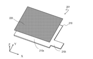
- FIG. 5 is an exploded perspective view of the electricity storage device electrode 201.
- the electricity storage device electrode 201 includes a current collector 210 and an active material layer 220 .
- Current collector 210 includes a first portion 210s and a second portion 210t, and active material layer 220 is disposed on first portion 210s.
- the second portion 210t is not provided with the active material layer 220 and functions as a tab for electrical connection to the outside.
- Active material layer 220 includes an active material that is oxidized and reduced during charging (or storage) and discharging.
- Current collector 210 supports active material layer 220 , supplies electrons to active material layer 220 , and receives electrons from active material layer 220 .
- the current collector 210 is the current collectors 101, 102, and 103 described in the first embodiment or the second embodiment. When current collector 103 is used, another active material layer not shown in FIG. .
- Active material layer 220 includes a positive electrode active material or a negative electrode active material that absorbs and releases lithium ions.
- the positive electrode active material includes, for example, a composite metal oxide containing lithium.
- the active material layer 220 may further contain at least one of a binder and a conductive aid.
- a binder Various known materials can be used for the binder. Binders in the active material layer 220 used for the positive electrode include polyvinylidene fluoride (PVDF), polytetrafluoroethylene (PTFE), tetrafluoroethylene-hexafluoropropylene copolymer (FEP), and tetrafluoroethylene-perfluoroalkyl vinyl ether.
- PVDF polyvinylidene fluoride
- PTFE polytetrafluoroethylene
- FEP tetrafluoroethylene-hexafluoropropylene copolymer
- tetrafluoroethylene-perfluoroalkyl vinyl ether tetrafluoroethylene-perfluoroalkyl vinyl ether.
- Fluorine such as copolymer (PFA), ethylene-tetrafluoroethylene copolymer (ETFE), polychlorotrifluoroethylene (PCTFE), ethylene-chlorotrifluoroethylene copolymer (ECTFE) and polyvinyl fluoride (PVF) Resin can be used.
- PFA copolymer
- ETFE ethylene-tetrafluoroethylene copolymer
- PCTFE polychlorotrifluoroethylene
- ECTFE ethylene-chlorotrifluoroethylene copolymer
- PVF polyvinyl fluoride
- a vinylidene fluoride-based fluorororubber may be used as the binder.
- vinylidene fluoride-hexafluoropropylene-based fluororubber VDF-HFP-based fluororubber
- vinylidene fluoride-hexafluoropropylene-tetrafluoroethylene-based fluororubber VDF-HFP-TFE-based fluororubber
- vinylidene fluoride- Pentafluoropropylene fluororubber VDF-PFP fluorubber
- vinylidene fluoride-pentafluoropropylene-tetrafluoroethylene fluororubber VDF-PFP-TFE fluorubber
- vinylidene fluoride-perfluoromethyl vinyl ether-tetra Fluoroethylene-based fluororubber VDF-PFMVE-TFE-based fluororubber
- Examples of conductive aids are carbon materials such as carbon powder and carbon nanotubes. Carbon black or the like can be applied to the carbon powder.
- Other examples of the conductive aid for the active material layer 220 used for the positive electrode are metal powders such as nickel, stainless steel and iron, and powders of conductive oxides such as ITO. Two or more of the above materials may be mixed and contained in the active material layer 220 .
- the negative electrode active material contains a carbon material.
- carbon materials include natural or artificial graphite, carbon nanotubes, non-graphitizable carbon, easily graphitizable carbon (soft carbon), low-temperature fired carbon, and the like.
- the negative electrode active material may contain materials other than the carbon material.
- alkali metals such as metallic lithium and alkaline earth metals, metals such as tin that can form compounds with metals such as lithium, silicon, silicon-carbon composites, amorphous compounds mainly composed of oxides (SiO x (0 ⁇ x ⁇ 2), tin dioxide, etc.), lithium titanate (Li 4 Ti 5 O 12 ), and other particles may be included.
- the binder and conductive aid of the active material layer 220 used for the negative electrode can be used in the same manner.
- Cellulose, styrene/butadiene rubber, ethylene/propylene rubber, polyimide, polyamideimide, acrylic resin, or the like may also be used as a binder for the negative electrode.
- the positive electrode and negative electrode for an electricity storage device can be manufactured by a known manufacturing method.
- the electricity storage device electrode of the present embodiment has high corrosion resistance to decomposition products of the electrolyte in the non-aqueous electrolyte. For this reason, even when the lithium ion secondary battery including the electricity storage device electrode of the present embodiment is used under conditions that facilitate decomposition of the electrolyte, for example, even when the lithium ion secondary battery is used at high temperatures, the battery characteristics due to deterioration of the current collector decrease in
- FIG. 6 is a schematic external view showing an example of the lithium ion secondary battery 301
- FIG. 7 is an exploded perspective view showing cells in the lithium ion secondary battery shown in FIG.
- a lithium ion secondary battery a pouch type or laminated type lithium ion secondary battery is exemplified.
- the illustrated lithium ion secondary battery is of a single layer type, but may be of a laminated type.
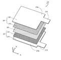
- the positive electrode, separator, and negative electrode that constitute the cell are stacked along the Z direction in the figure.
- a lithium ion secondary battery 301 includes a cell 310 , a pair of leads 311 connected to the cell 310 , an exterior body 313 covering the cell 310 , and an electrolyte 314 .
- the cell 310 includes an electricity storage device electrode 201, an electricity storage device electrode 201', and a separator 320 arranged therebetween.
- cell 310 is a single layer cell that includes a pair of electrodes.
- the power storage device electrode 201 and the power storage device electrode 201′ are the power storage device electrode 201 described in the third embodiment, one of which is a positive electrode containing a positive electrode active material, and the other is a negative electrode containing a negative electrode active material. It is configured.
- the separator 320 is an insulating porous material.
- Nonwoven fabrics, porous films, and the like can be used.
- the electrolyte 314 is further arranged in the space inside the exterior body 313 .
- the electrolyte 314 is a non-aqueous electrolyte containing lithium ions, such as a non-aqueous electrolytic solution containing lithium ions.
- a sealing material for example, a resin film such as polypropylene
- a resin film such as polypropylene
- a nonaqueous electrolytic solution containing a metal salt such as a lithium salt and an organic solvent can be used.
- Lithium salts include, for example, LiPF6 , LiClO4, LiBF4 , LiCF3SO3 , LiCF3CF2SO3 , LiC( CF3SO2 ) 3 , LiN( CF3SO2 ) 2 , LiN( CF3 CF2SO2 ) 2 , LiN( CF3SO2 )( C4F9SO2 ) , LiN( CF3CF2CO ) 2 , LiBOB and the like can be used.
- LiPF6 LiClO4, LiBF4 , LiCF3SO3 , LiCF3CF2SO3 , LiC( CF3SO2 ) 3 , LiN( CF3SO2 ) 2 , LiN( CF3 CF2SO2 ) 2 , LiN( CF3SO2 )( C4F9SO2 ) , Li
- cyclic carbonate and chain carbonate can be used.
- ethylene carbonate, propylene carbonate, butylene carbonate, dimethyl carbonate and the like can be used.
- the lithium ion secondary battery 301 can be manufactured, for example, by the following method. First, electrodes 201 and 201' are fabricated as described in the above embodiment. After that, the electrode 201 and the electrode 201 ′ are held so that the active material layers face each other with the separator 320 interposed therebetween, and inserted into the space of the exterior body 313 . Lithium ion secondary battery 301 is completed by arranging electrolyte 314 in the space of package 313 and sealing package 313 .
- the lithium-ion secondary battery 301 has high corrosion resistance against decomposition products of the electrolyte in the non-aqueous electrolyte. Therefore, even when the lithium ion secondary battery is used at high temperatures, deterioration of battery characteristics due to deterioration of the current collector is suppressed.
- Example A current collector of an example and a current collector of a reference example were produced and their properties were evaluated.
- a current collector 102 having the structure shown in FIG. 3 was produced.
- a polyethylene terephthalate resin having a thickness of 5 ⁇ m was used for the resin layer 10 .
- the first intermediate layer 31 and the second intermediate layer 32 were formed by a sputtering method using the metals or metal oxides shown in Tables 3 to 6 as targets. The thicknesses of the first intermediate layer 31 and the second intermediate layer 32 were adjusted by the deposition time and power.
- the Cu conductive layer 20 was formed separately into a seed layer 21 and a main layer 22 . After forming the seed layer 21 with a thickness of 50 nm, the main layer 22 with a thickness shown in Tables 3 to 6 was formed by electroplating.
- the conductive layers of Al and Cu--Ni were formed with the thicknesses shown in Tables 3 to 6 by a sputtering method.
- the molar ratio of metal to oxygen was controlled to be 1:1.
- a metal carbide was also used as the target.
- the composition ratio in the metal oxide was confirmed by composition analysis using X-ray photoelectron spectroscopy (XPS).
- the current collectors of Reference Examples 1 to 4 were produced without forming at least one of the first intermediate layer and the second intermediate layer.
- the (111) plane orientation index of the conductive layer was measured by the X-ray diffraction method, and obtained by the orientation index F according to the Lotgering method described above.
- the apparatus and measurement conditions used for the measurement are as follows.
- Measurement Method Out of Plane
- Examples 1 to 24 and Reference Examples 1 to 4 were held in an environment similar to that of a lithium ion secondary battery, and peeling of the conductive layer and corrosion of the conductive layer were evaluated. Specifically, an electrolytic solution of dimethyl carbonate containing LiPF 6 at a concentration of 1 mol % was prepared. Further, an electrolytic solution 1 was prepared by adding water to the electrolytic solution at a rate of 1000 ppm by mass. Similarly, electrolyte solution 2 was prepared with the amount of water to be added at a rate of 3000 ppm by mass, and electrolyte solution 3 was prepared by adjusting the amount of water to be added at a rate of 5000 ppm by mass.
- any one of electrolyte solutions 1 to 3 was placed in a container, the prepared current collector was immersed in the electrolyte solution in the container, the whole was sealed with a laminate film, and stored in a constant temperature bath at 85°C for 72 hours. After that, the current collector was taken out from the laminate film and washed with an organic solvent.
- Corrosion resistance was evaluated by observing the surface resistance of the conductive layer and an optical microscope.
- the surface resistance of the conductive layer was measured with a low resistance resistivity meter (trade name: Loresta GX MCP-T700, manufactured by Nitto Seiko Analytic Tech). Observation with an optical microscope was performed at a magnification of 100 to 200 times, arbitrary three observation areas were selected, and determination was made as to whether or not holes were formed in the selected areas.
- the surface resistance value of the conductive layer increases by 20% or more compared to before high-temperature storage, or if holes are found in the conductive layer by observation, it is determined to be unacceptable (POOR), and the increase in resistance value is 20%. % and no hole was found in the conductive layer, it was determined as GOOD.
- Peeling resistance was evaluated by two methods. The surface of the conductive layer of the current collector after high-temperature storage was rubbed with a cotton swab, and when a part of the conductive layer adhered to the cotton swab, it was determined that the conductive layer had separated from the resin layer, and it was determined to be unsatisfactory (POOR). In addition, an adhesive tape having an adhesive force of 4 N/cm was attached to the surface of the conductive layer of the current collector after high-temperature storage, and whether or not the conductive layer adhered was examined. When no peeling by the cotton swab was observed, but adhesion by the adhesive tape was observed, it was judged to be good (GOOD). When neither peeling with a cotton swab nor adhesion with an adhesive tape was observed, it was judged as excellent (EXCELLENT).
- Table 2 summarizes the produced current collector, the electrolyte used for storage, and the evaluation performed. Evaluation results are shown in Tables 3 to 6.
- the conductive layer when the thickness of the first intermediate layer is 1 nm or more and 120 nm or less, the conductive layer can obtain good corrosion resistance and peeling resistance. In particular, when the thickness of the first intermediate layer is 2 nm or more and 100 nm or less, the conductive layer has excellent corrosion resistance and peeling resistance. Further, from Tables 3 and 4, it can be seen that if D1/D2, which is the ratio of the first intermediate layer to the second intermediate layer, satisfies D1/D2 ⁇ 10, a current collector excellent in both peel resistance and corrosion resistance can be obtained. It is understood that Furthermore, it can be seen that when D1/D2 satisfies 2 ⁇ D1/D2 ⁇ 10, the current collector is more excellent in peel resistance and corrosion resistance.
- the surface energy of Ag which is the metal of the first intermediate layer
- the energy of Cu which is the metal of the conductive layer
- the surface energy of the metal of the first intermediate layer is higher than the energy of the metal of the conductive layer.
- the (111) plane orientation index is as small as 0.25 in the current collector of Example 16, and the current collectors of Examples 14, 15, and 17 to 20, which are examples other than Example 16, has a large value of 0.65 or more. This is considered to indicate that the magnitude relationship of the surface energy of the metal between the first intermediate layer and the conductive layer affects the ease of (111) plane orientation, as described above.
- the metals constituting the first intermediate layer are various such as Cr, Mo, Co, Ni—Cr, and W.
- the (111) plane orientation index is large in any of the current collectors. This is considered to indicate that the lattice constant of the crystal of the metal forming the first intermediate layer and the crystallinity of the first intermediate layer have little effect on the (111) plane orientation index.
- the current collectors of Examples 14, 15, and 17 to 20 have improved corrosion resistance of the conductive layers. This is considered to indicate that there is a correlation between the value of the (111) plane orientation index of the conductive layer and the corrosion resistance.
- the conductive layer is effectively conductive. It is thought that the orientation of the (111) plane of the layer can be enhanced, and the corrosion resistance can be improved.
- the current collector of the present embodiment has corrosion resistance and peeling resistance against decomposition products of the electrolyte in the non-aqueous electrolyte by including the first intermediate layer and the second intermediate layer. was found to be able to increase
- the power storage device electrodes according to the embodiments of the present disclosure are useful as power sources for various electronic devices, electric motors, and the like.
- Power storage devices according to embodiments of the present disclosure include, for example, power sources for vehicles typified by bicycles and passenger cars, power sources for communication devices typified by smartphones, power sources for various sensors, unmanned eXtended vehicles ( UxV)) power supply.
- UxV unmanned eXtended vehicles
Landscapes
- Chemical & Material Sciences (AREA)
- Engineering & Computer Science (AREA)
- Chemical Kinetics & Catalysis (AREA)
- Electrochemistry (AREA)
- General Chemical & Material Sciences (AREA)
- Materials Engineering (AREA)
- Manufacturing & Machinery (AREA)
- Composite Materials (AREA)
- Cell Electrode Carriers And Collectors (AREA)
Priority Applications (4)
| Application Number | Priority Date | Filing Date | Title |
|---|---|---|---|
| PCT/JP2021/036089 WO2023053322A1 (ja) | 2021-09-30 | 2021-09-30 | 集電体、蓄電デバイス用電極およびリチウムイオン二次電池 |
| CN202180102841.1A CN118044007A (zh) | 2021-09-30 | 2021-09-30 | 集电体、蓄电器件用电极及锂离子二次电池 |
| JP2023550889A JP7796135B2 (ja) | 2021-09-30 | 2021-09-30 | 集電体、蓄電デバイス用電極およびリチウムイオン二次電池 |
| US18/696,750 US20240379969A1 (en) | 2021-09-30 | 2021-09-30 | Current collector, electrode for electric storage device, and lithium-ion secondary battery |
Applications Claiming Priority (1)
| Application Number | Priority Date | Filing Date | Title |
|---|---|---|---|
| PCT/JP2021/036089 WO2023053322A1 (ja) | 2021-09-30 | 2021-09-30 | 集電体、蓄電デバイス用電極およびリチウムイオン二次電池 |
Publications (1)
| Publication Number | Publication Date |
|---|---|
| WO2023053322A1 true WO2023053322A1 (ja) | 2023-04-06 |
Family
ID=85781580
Family Applications (1)
| Application Number | Title | Priority Date | Filing Date |
|---|---|---|---|
| PCT/JP2021/036089 Ceased WO2023053322A1 (ja) | 2021-09-30 | 2021-09-30 | 集電体、蓄電デバイス用電極およびリチウムイオン二次電池 |
Country Status (4)
| Country | Link |
|---|---|
| US (1) | US20240379969A1 (https=) |
| JP (1) | JP7796135B2 (https=) |
| CN (1) | CN118044007A (https=) |
| WO (1) | WO2023053322A1 (https=) |
Cited By (2)
| Publication number | Priority date | Publication date | Assignee | Title |
|---|---|---|---|---|
| WO2025141819A1 (ja) * | 2023-12-27 | 2025-07-03 | TeraWatt Technology株式会社 | リチウム2次電池 |
| WO2025248599A1 (ja) * | 2024-05-27 | 2025-12-04 | Tdk株式会社 | 集電体、電極及びリチウムイオン二次電池 |
Citations (6)
| Publication number | Priority date | Publication date | Assignee | Title |
|---|---|---|---|---|
| JP2003282064A (ja) * | 2002-03-20 | 2003-10-03 | Toyo Kohan Co Ltd | 複合集電体 |
| JP2004273304A (ja) * | 2003-03-10 | 2004-09-30 | Matsushita Electric Ind Co Ltd | 電極とこれを用いた電池 |
| JP2010176987A (ja) * | 2009-01-28 | 2010-08-12 | Nissan Motor Co Ltd | 双極型二次電池 |
| JP2013026192A (ja) * | 2011-07-26 | 2013-02-04 | Nissan Motor Co Ltd | 双極型リチウムイオン二次電池用集電体 |
| JP2016207542A (ja) * | 2015-04-24 | 2016-12-08 | 昭和電工パッケージング株式会社 | 蓄電デバイス用外装体及び蓄電デバイス |
| WO2021145344A1 (ja) * | 2020-01-17 | 2021-07-22 | 富士フイルム株式会社 | 非水電解質二次電池、集電体、及び非水電解質二次電池の製造方法 |
-
2021
- 2021-09-30 CN CN202180102841.1A patent/CN118044007A/zh active Pending
- 2021-09-30 WO PCT/JP2021/036089 patent/WO2023053322A1/ja not_active Ceased
- 2021-09-30 US US18/696,750 patent/US20240379969A1/en active Pending
- 2021-09-30 JP JP2023550889A patent/JP7796135B2/ja active Active
Patent Citations (6)
| Publication number | Priority date | Publication date | Assignee | Title |
|---|---|---|---|---|
| JP2003282064A (ja) * | 2002-03-20 | 2003-10-03 | Toyo Kohan Co Ltd | 複合集電体 |
| JP2004273304A (ja) * | 2003-03-10 | 2004-09-30 | Matsushita Electric Ind Co Ltd | 電極とこれを用いた電池 |
| JP2010176987A (ja) * | 2009-01-28 | 2010-08-12 | Nissan Motor Co Ltd | 双極型二次電池 |
| JP2013026192A (ja) * | 2011-07-26 | 2013-02-04 | Nissan Motor Co Ltd | 双極型リチウムイオン二次電池用集電体 |
| JP2016207542A (ja) * | 2015-04-24 | 2016-12-08 | 昭和電工パッケージング株式会社 | 蓄電デバイス用外装体及び蓄電デバイス |
| WO2021145344A1 (ja) * | 2020-01-17 | 2021-07-22 | 富士フイルム株式会社 | 非水電解質二次電池、集電体、及び非水電解質二次電池の製造方法 |
Cited By (2)
| Publication number | Priority date | Publication date | Assignee | Title |
|---|---|---|---|---|
| WO2025141819A1 (ja) * | 2023-12-27 | 2025-07-03 | TeraWatt Technology株式会社 | リチウム2次電池 |
| WO2025248599A1 (ja) * | 2024-05-27 | 2025-12-04 | Tdk株式会社 | 集電体、電極及びリチウムイオン二次電池 |
Also Published As
| Publication number | Publication date |
|---|---|
| US20240379969A1 (en) | 2024-11-14 |
| JPWO2023053322A1 (https=) | 2023-04-06 |
| JP7796135B2 (ja) | 2026-01-08 |
| CN118044007A (zh) | 2024-05-14 |
Similar Documents
| Publication | Publication Date | Title |
|---|---|---|
| CN109716562B (zh) | 锂离子二次电池 | |
| TWI695537B (zh) | 低熔融溫度金屬純化與沉積 | |
| CN109994739A (zh) | 负极极片与包含其的电化学装置及电子装置 | |
| CN108028383A (zh) | 用于电池组单元的经涂覆的阴极活性材料 | |
| JP2008269972A (ja) | 非水溶媒二次電池 | |
| JP5920217B2 (ja) | 二次電池 | |
| JP2014225326A (ja) | 非水電解質二次電池 | |
| EP4024503A1 (en) | Lithium secondary battery | |
| KR100866863B1 (ko) | 리튬 이차 전지용 음극, 이의 제조방법 및 이를 포함하는리튬 이차 전지 | |
| MX2013013478A (es) | Material activo de electrodos negativos para dispositivo electrico. | |
| CN102623709A (zh) | 电池 | |
| EP4636892A1 (en) | Electrolyte for lithium secondary battery and lithium secondary battery comprising same | |
| JP7796135B2 (ja) | 集電体、蓄電デバイス用電極およびリチウムイオン二次電池 | |
| JP5561774B2 (ja) | 非水電解液二次電池の製造方法 | |
| US20250183322A1 (en) | Current collector, electrode for power storage device, and lithium ion secondary battery | |
| JPWO2013042421A1 (ja) | 二次電池 | |
| CN111837261A (zh) | 电极组、电池及电池包 | |
| JPWO2012049889A1 (ja) | 二次電池およびそれに用いる二次電池用電解液 | |
| WO2022176094A1 (ja) | 積層樹脂フィルム、集電体および二次電池 | |
| WO2023135818A1 (ja) | 集電体、蓄電デバイス用電極およびリチウムイオン二次電池、ならびに集電体の製造方法 | |
| JPWO2012029645A1 (ja) | 二次電池およびそれに用いる二次電池用電解液 | |
| JP7830122B2 (ja) | 集電体、蓄電デバイス用電極、リチウムイオン二次電池および集電体の製造方法 | |
| KR20230087039A (ko) | 리튬 이차 전지 | |
| JP7311027B2 (ja) | 蓄電デバイス用電極およびリチウムイオン二次電池 | |
| WO2013183525A1 (ja) | リチウムイオン二次電池 |
Legal Events
| Date | Code | Title | Description |
|---|---|---|---|
| 121 | Ep: the epo has been informed by wipo that ep was designated in this application |
Ref document number: 21959364 Country of ref document: EP Kind code of ref document: A1 |
|
| WWE | Wipo information: entry into national phase |
Ref document number: 2023550889 Country of ref document: JP |
|
| WWE | Wipo information: entry into national phase |
Ref document number: 202180102841.1 Country of ref document: CN Ref document number: 18696750 Country of ref document: US |
|
| NENP | Non-entry into the national phase |
Ref country code: DE |
|
| 122 | Ep: pct application non-entry in european phase |
Ref document number: 21959364 Country of ref document: EP Kind code of ref document: A1 |