WO2023042315A1 - 波長変換素子 - Google Patents
波長変換素子 Download PDFInfo
- Publication number
- WO2023042315A1 WO2023042315A1 PCT/JP2021/033985 JP2021033985W WO2023042315A1 WO 2023042315 A1 WO2023042315 A1 WO 2023042315A1 JP 2021033985 W JP2021033985 W JP 2021033985W WO 2023042315 A1 WO2023042315 A1 WO 2023042315A1
- Authority
- WO
- WIPO (PCT)
- Prior art keywords
- wavelength conversion
- conversion element
- core
- optical axis
- axis direction
- Prior art date
- Legal status (The legal status is an assumption and is not a legal conclusion. Google has not performed a legal analysis and makes no representation as to the accuracy of the status listed.)
- Ceased
Links
Images




Classifications
-
- G—PHYSICS
- G02—OPTICS
- G02F—OPTICAL DEVICES OR ARRANGEMENTS FOR THE CONTROL OF LIGHT BY MODIFICATION OF THE OPTICAL PROPERTIES OF THE MEDIA OF THE ELEMENTS INVOLVED THEREIN; NON-LINEAR OPTICS; FREQUENCY-CHANGING OF LIGHT; OPTICAL LOGIC ELEMENTS; OPTICAL ANALOGUE/DIGITAL CONVERTERS
- G02F1/00—Devices or arrangements for the control of the intensity, colour, phase, polarisation or direction of light arriving from an independent light source, e.g. switching, gating or modulating; Non-linear optics
- G02F1/35—Non-linear optics
- G02F1/37—Non-linear optics for second-harmonic generation
- G02F1/377—Non-linear optics for second-harmonic generation in an optical waveguide structure
-
- G—PHYSICS
- G02—OPTICS
- G02F—OPTICAL DEVICES OR ARRANGEMENTS FOR THE CONTROL OF LIGHT BY MODIFICATION OF THE OPTICAL PROPERTIES OF THE MEDIA OF THE ELEMENTS INVOLVED THEREIN; NON-LINEAR OPTICS; FREQUENCY-CHANGING OF LIGHT; OPTICAL LOGIC ELEMENTS; OPTICAL ANALOGUE/DIGITAL CONVERTERS
- G02F1/00—Devices or arrangements for the control of the intensity, colour, phase, polarisation or direction of light arriving from an independent light source, e.g. switching, gating or modulating; Non-linear optics
- G02F1/01—Devices or arrangements for the control of the intensity, colour, phase, polarisation or direction of light arriving from an independent light source, e.g. switching, gating or modulating; Non-linear optics for the control of the intensity, phase, polarisation or colour
- G02F1/03—Devices or arrangements for the control of the intensity, colour, phase, polarisation or direction of light arriving from an independent light source, e.g. switching, gating or modulating; Non-linear optics for the control of the intensity, phase, polarisation or colour based on ceramics or electro-optical crystals, e.g. exhibiting Pockels effect or Kerr effect
- G02F1/035—Devices or arrangements for the control of the intensity, colour, phase, polarisation or direction of light arriving from an independent light source, e.g. switching, gating or modulating; Non-linear optics for the control of the intensity, phase, polarisation or colour based on ceramics or electro-optical crystals, e.g. exhibiting Pockels effect or Kerr effect in an optical waveguide structure
-
- G—PHYSICS
- G02—OPTICS
- G02F—OPTICAL DEVICES OR ARRANGEMENTS FOR THE CONTROL OF LIGHT BY MODIFICATION OF THE OPTICAL PROPERTIES OF THE MEDIA OF THE ELEMENTS INVOLVED THEREIN; NON-LINEAR OPTICS; FREQUENCY-CHANGING OF LIGHT; OPTICAL LOGIC ELEMENTS; OPTICAL ANALOGUE/DIGITAL CONVERTERS
- G02F1/00—Devices or arrangements for the control of the intensity, colour, phase, polarisation or direction of light arriving from an independent light source, e.g. switching, gating or modulating; Non-linear optics
- G02F1/35—Non-linear optics
- G02F1/3501—Constructional details or arrangements of non-linear optical devices, e.g. shape of non-linear crystals
-
- G—PHYSICS
- G02—OPTICS
- G02F—OPTICAL DEVICES OR ARRANGEMENTS FOR THE CONTROL OF LIGHT BY MODIFICATION OF THE OPTICAL PROPERTIES OF THE MEDIA OF THE ELEMENTS INVOLVED THEREIN; NON-LINEAR OPTICS; FREQUENCY-CHANGING OF LIGHT; OPTICAL LOGIC ELEMENTS; OPTICAL ANALOGUE/DIGITAL CONVERTERS
- G02F1/00—Devices or arrangements for the control of the intensity, colour, phase, polarisation or direction of light arriving from an independent light source, e.g. switching, gating or modulating; Non-linear optics
- G02F1/35—Non-linear optics
- G02F1/353—Frequency conversion, i.e. wherein a light beam is generated with frequency components different from those of the incident light beams
- G02F1/3544—Particular phase matching techniques
- G02F1/3548—Quasi phase matching [QPM], e.g. using a periodic domain inverted structure
-
- G—PHYSICS
- G02—OPTICS
- G02F—OPTICAL DEVICES OR ARRANGEMENTS FOR THE CONTROL OF LIGHT BY MODIFICATION OF THE OPTICAL PROPERTIES OF THE MEDIA OF THE ELEMENTS INVOLVED THEREIN; NON-LINEAR OPTICS; FREQUENCY-CHANGING OF LIGHT; OPTICAL LOGIC ELEMENTS; OPTICAL ANALOGUE/DIGITAL CONVERTERS
- G02F1/00—Devices or arrangements for the control of the intensity, colour, phase, polarisation or direction of light arriving from an independent light source, e.g. switching, gating or modulating; Non-linear optics
- G02F1/35—Non-linear optics
- G02F1/355—Non-linear optics characterised by the materials used
- G02F1/3551—Crystals
-
- G—PHYSICS
- G02—OPTICS
- G02F—OPTICAL DEVICES OR ARRANGEMENTS FOR THE CONTROL OF LIGHT BY MODIFICATION OF THE OPTICAL PROPERTIES OF THE MEDIA OF THE ELEMENTS INVOLVED THEREIN; NON-LINEAR OPTICS; FREQUENCY-CHANGING OF LIGHT; OPTICAL LOGIC ELEMENTS; OPTICAL ANALOGUE/DIGITAL CONVERTERS
- G02F1/00—Devices or arrangements for the control of the intensity, colour, phase, polarisation or direction of light arriving from an independent light source, e.g. switching, gating or modulating; Non-linear optics
- G02F1/35—Non-linear optics
- G02F1/365—Non-linear optics in an optical waveguide structure
-
- G—PHYSICS
- G02—OPTICS
- G02F—OPTICAL DEVICES OR ARRANGEMENTS FOR THE CONTROL OF LIGHT BY MODIFICATION OF THE OPTICAL PROPERTIES OF THE MEDIA OF THE ELEMENTS INVOLVED THEREIN; NON-LINEAR OPTICS; FREQUENCY-CHANGING OF LIGHT; OPTICAL LOGIC ELEMENTS; OPTICAL ANALOGUE/DIGITAL CONVERTERS
- G02F1/00—Devices or arrangements for the control of the intensity, colour, phase, polarisation or direction of light arriving from an independent light source, e.g. switching, gating or modulating; Non-linear optics
- G02F1/35—Non-linear optics
- G02F1/37—Non-linear optics for second-harmonic generation
- G02F1/377—Non-linear optics for second-harmonic generation in an optical waveguide structure
- G02F1/3775—Non-linear optics for second-harmonic generation in an optical waveguide structure with a periodic structure, e.g. domain inversion, for quasi-phase-matching [QPM]
-
- G—PHYSICS
- G02—OPTICS
- G02F—OPTICAL DEVICES OR ARRANGEMENTS FOR THE CONTROL OF LIGHT BY MODIFICATION OF THE OPTICAL PROPERTIES OF THE MEDIA OF THE ELEMENTS INVOLVED THEREIN; NON-LINEAR OPTICS; FREQUENCY-CHANGING OF LIGHT; OPTICAL LOGIC ELEMENTS; OPTICAL ANALOGUE/DIGITAL CONVERTERS
- G02F2202/00—Materials and properties
- G02F2202/20—LiNbO3, LiTaO3
Definitions
- the present disclosure relates to wavelength conversion elements, and more specifically to wavelength conversion elements using nonlinear optical effects.
- Wavelength conversion technology using the second-order nonlinear optical effect has been put to practical use in fields such as optical processing, medical care, and biotechnology, in addition to wavelength conversion of optical signals in optical communications.
- a light source that outputs light in a wavelength range that cannot be directly output by a semiconductor laser in the ultraviolet, visible, infrared, or terahertz range, or a wavelength range that can be directly output by a semiconductor laser cannot be obtained by a semiconductor laser.
- An example of its application is a light source that requires a high output intensity.
- a wavelength conversion element having a periodically poled optical waveguide to which lithium niobate (LiNbO 3 : hereinafter referred to as LN) having a high nonlinear constant is applied is a light source already on the market due to its high wavelength conversion efficiency. Practical use is progressing as
- DFG Difference Frequency Generation
- Equation 3 There is also an optical parametric effect that inputs only ⁇ 1 and generates ⁇ 2 and ⁇ 3 that satisfy (Equation 3).
- SHG and SFG newly generate light with a shorter wavelength than incident light, that is, light with high energy, and are often used to generate visible light.
- DFG converts short-wavelength light into long-wavelength light and is often used to generate light in the mid-infrared region and longer wavelengths.
- phase mismatch amount for the three interacting lights is required to be zero.
- a periodically poled structure can be used as a method for making the amount of phase mismatch quasi-zero.
- FIG. 1 is a perspective view conceptually showing a conventional wavelength conversion element 10 having a periodically poled structure.
- a wavelength conversion element 10 having a periodically poled structure includes a substrate 11 and a core 12 bonded on the substrate for wavelength conversion of incident light. Further, the core 12 has a region 121 in which the nonlinear constant has a positive value (hereinafter referred to as a positive core region) and a region 122 in which the nonlinear constant has a negative value (hereinafter referred to as a negative core region). It has an alternating structure.
- the periodically poled structure is thus a structure in which positive and negative nonlinear constants are alternately switched by periodically reversing the spontaneous polarization of the second-order nonlinear optical material in the optical axis direction. Assuming that this inversion period is ⁇ , in the sum frequency generation shown in (Equation 1), if ⁇ is set so as to satisfy (Equation 4) for wavelengths ⁇ 1 , ⁇ 2 , and ⁇ 3 , then The phase mismatch amount can be set to 0 in a pseudo manner.
- ridge-type waveguides in which the core is bonded to the substrate, can utilize the characteristics of the crystal bulk applied to the core as they are, so they are excellent in terms of high resistance to optical damage, long-term reliability, and ease of device design, and are being actively researched. Development is underway (see, for example, Non-Patent Document 1).
- a wavelength conversion element having a ridge-shaped waveguide structure is obtained by bonding a core partially formed with a periodically poled structure that satisfies a phase matching condition in a predetermined wavelength band in advance to a substrate that holds the core. is thinned and then processed into a ridge.
- adhesives were used to join the core and the substrate, but in recent years, direct bonding technology has been applied to achieve high-strength bonding and suppress separation cracks at the bonding interface, thereby improving the wavelength conversion element. Further efficiency and longevity have been achieved.
- the incident light to be guided and the converted light to be emitted are wavelength-converted TM (Transverse Magnetic Wave) polarized light in which the optical electric field is polarized in the direction perpendicular to the substrate. ing.
- TM Transverse Magnetic Wave
- the wavelength conversion element with an LN crystal applied to the core performs wavelength conversion by DFG at 25° C., which is near room temperature.
- the wavelength of the converted light emitted from the wavelength conversion element is ⁇ 3 becomes 2.94 ⁇ m.
- the poling period ⁇ for phase matching is calculated as 28.48 ⁇ m from (Equation 4) using the relationship of the refractive index dispersion of LN at each light wavelength. be. That is, if the core structure is such that the spontaneous polarization of the LN is reversed with a period of 28.48 ⁇ m with respect to the optical axis direction, wavelength conversion is performed with high efficiency.
- the nonlinear constant can only take values of +d or ⁇ d, and cannot take intermediate values.
- the converted light having an unintended wavelength is defined as a new poling period obtained by dividing the poling period ⁇ such as ⁇ /3 or ⁇ /5 by an odd integer. is generated.
- Non-Patent Document 1 As a conventional technique for suppressing such unintended wavelength conversion that occurs parasitically, there is a method of inserting a phase adjustment layer into the core (see, for example, Non-Patent Document 1). However, in such a conventional method for suppressing parasitic wavelength conversion, parasitic wavelength conversion occurs until it reaches the phase adjustment layer. strength decreases. That is, parasitic wavelength conversion cannot be efficiently suppressed, and there is a problem that the intensity of the intended wavelength-converted light is not a little reduced.
- the present disclosure has been made in view of the above problems, and an object thereof is to provide a wavelength conversion element capable of suppressing unintended wavelength conversion due to high-order quasi-phase matching. be.
- the present disclosure provides a wavelength conversion element using a second-order nonlinear optical effect, which includes a substrate and a core that is bonded to the substrate and performs wavelength conversion of incident light. , a structure in which the first spontaneous polarization and the second spontaneous polarization are periodically reversed with respect to the optical axis direction, and in the region having the first spontaneous polarization and the region having the second spontaneous polarization, the core
- a wavelength conversion element having a structure in which the cross-sectional area changes with respect to the optical axis direction so that the cross-sectional area is maximized at the ends and minimized at the center.
- FIG. 1 is a perspective view conceptually showing a conventional wavelength conversion element having a periodically poled structure
- FIG. FIG. 2A is a diagram showing modulation curves in a wavelength conversion element
- FIG. 2A is a modulation curve when using a wavelength conversion element according to the prior art
- FIG. ideal modulation curves for It is a conceptual diagram showing the structure of the wavelength conversion element by this indication
- Fig.3 (a) is a perspective view
- FIG.3(b) has shown the top view, respectively.
- FIG. 12 conceptually illustrates a modulation curve in the core of a wavelength conversion element according to an embodiment of the present disclosure
- FIG. 5 is a diagram showing calculation results of a phase matching pattern when using a conventional wavelength conversion element and a wavelength conversion element according to the present disclosure
- FIG. 6 is a conceptual diagram showing the structure of the wavelength conversion element according to the present disclosure
- FIG. 6(a) showing a perspective view
- FIG. 6(b) showing a front view
- 7A and 7B are conceptual diagrams showing the structure of the wavelength conversion element 70 according to the present disclosure, where FIG. 7A is a perspective view
- FIG. 7B is a top view
- FIG. 7C is a front view.
- It is a conceptual diagram showing the structure of the wavelength conversion element 80 according to the present disclosure
- FIG. 8(a) is a perspective view
- FIG. 8(b) is a top view.
- This disclosure proposes a wavelength conversion element that is configured to perform modulation such that the wavelength conversion efficiency decreases for unintended wavelength conversion. Moreover, in order to reduce the wavelength efficiency for unintended wavelength conversion, the cross-sectional area of the core through which light propagates varies with respect to the optical axis direction, which is different from the prior art.
- the wavelength conversion efficiency of a waveguide-type wavelength conversion element depends on the nonlinear constant, length, and cross-sectional area of the core that constitutes the waveguide (specifically, it is proportional to the square of the nonlinear constant and the square of the length). and inversely proportional to the cross-sectional area).
- the core nonlinear constant is a material-dependent parameter, it is practically difficult to change.
- the length of the core is limited by the size of the substrate, it is also difficult to change. Therefore, in the wavelength conversion element according to the present disclosure, the efficiency of unintended wavelength conversion is reduced by changing the cross-sectional area of the core.
- FIG. 2A and 2B are diagrams showing modulation curves in a wavelength conversion element
- FIG. 2A is a modulation curve when using a conventional wavelength conversion element
- FIG. The ideal modulation curves for suppressing conversion are shown respectively.
- the core has a structure in which the cross-sectional area is constant in the optical axis direction.
- the nonlinear constant takes only two values of +d or -d, so the modulation curve is a rectangular function.
- the modulation curve should ideally be a sine function with a nonlinear constant of 0 at the interface where the spontaneous polarization of the core is reversed. This is because in the Fourier series expansion described above, if the original function is a sine function, no higher-order terms are generated.
- the present disclosure proposes a wavelength conversion element having a structure in which the cross-sectional area is large at the ends in the optical axis direction and the cross-sectional area is small at the center in one region having spontaneous polarization. do.
- the modulation curve has a shape close to a sine function with a peak at the central portion in the optical axis direction. Therefore, it is possible to reduce the wavelength conversion efficiency for unintended wavelength conversion.
- the wavelength conversion element according to this embodiment has a structure in which the cross-sectional area of the core in the optical axis direction has a maximum value at the ends and a minimum value at the center, and the cross-sectional area changes linearly from the ends to the center.
- a wavelength converting element 30 according to the present disclosure includes a substrate 31 and a core 32 bonded onto the substrate to perform wavelength conversion of incident light. Furthermore, the core 32 includes a positive core region 321 and a negative core region 322, and has a periodically poled structure in which the positive core region 321 and the negative core region 322 are periodically reversed with respect to the optical axis direction. have. Moreover, as shown in FIG. 3B, each of the positive core region 321 and the negative core region 322 has a maximum cross-sectional area at the end of each core region in the optical axis direction.
- each core region has a constant height (the length in the direction perpendicular to the main surface of the substrate 31) and a width (the direction perpendicular to the main surface of the substrate 31 and the direction perpendicular to the optical axis). length) decreases at a constant rate from one end toward the center, and increases at a constant rate from the center toward the other end.
- the width of each core region varies (that is, decreases and increases) axisymmetrically about the centerline of the core region parallel to the optical axis direction.
- the cross-section of each core region is rectangular.
- the wavelength conversion element 30 in this embodiment uses lithium tantalate (LiTaO 3 , hereinafter referred to as LT) for the substrate 31 and LN for the core 32.
- the core 32 has a thickness of 1 ⁇ m and a length of is 12 mm.
- the width Wmax of the position where the cross-sectional area is maximized (that is, the edge) is set to 16 ⁇ m, and the position where the cross-sectional area is minimized (that is, the center)
- the width Wmin of is set to 8 ⁇ m.
- the substrate 31 and the core 32 are joined by direct joining. It is also assumed that the core 32 is formed by patterning a resist in advance by lithography so as to have the above-described shape, and by dry etching along the pattern.
- the manufacturing method is not limited to this, and for example, a laser ablation method or the like may be applied in which a high-intensity laser is irradiated to evaporate the core in order to shape the core as described above.
- the wavelength conversion efficiency changes in each of the positive core region 321 and the negative core region 322 according to the distance with respect to the optical axis direction. Therefore, the core 32 of the wavelength conversion element 30 behaves as if the nonlinear constant continuously changes in the optical axis direction.
- a nonlinear constant which is assumed to change artificially with a change in cross-sectional area is referred to as an "apparent nonlinear constant".
- FIG. 4 is a diagram conceptually showing modulation curves in the core 32 of the wavelength conversion element 30 according to one embodiment of the present disclosure.
- the vertical axis is the apparent nonlinear constant.
- the wavelength modulation curve is not rectangular, but has a mountain-shaped waveform with an apparent nonlinear constant peaking at the center of each core region. have. Therefore, the Fourier series expansion as shown in (Equation 5) reduces high-order sin components such as sin(3x) and sin(5x), and reduces the efficiency of wavelength conversion due to unintended quasi-phase matching. .
- FIG. 5 is a diagram showing calculation results of a phase matching pattern when using the wavelength conversion element 10 according to the prior art and the wavelength conversion element 30 according to the present disclosure.
- the horizontal axis in the figure is the normalized phase mismatch amount, and this value may be considered as the order of quasi-phase matching. Note that the reversal of spontaneous polarization is 1000 cycles.
- the width of the core 12 of the wavelength conversion element 10 according to the prior art is constant at 8 ⁇ m, and other dimensions are the same as those of the wavelength conversion element 30 according to the present disclosure described above.
- the wavelength conversion efficiency is generally reduced, especially in higher orders such as 3rd and 5th order. decrease is remarkable.
- the wavelength conversion efficiency when using the wavelength conversion element 30 according to the present disclosure has a reduction rate of 33% in the first order. 84% decrease in the 3rd and 68% decrease in the 5th. From this, it can be seen that the wavelength conversion element 30 according to the present disclosure can reduce the conversion efficiency of unintended wavelength conversion due to high-order quasi-phase matching. Although the primary (desired) wavelength conversion efficiency is also reduced, this can be improved by increasing the power of the incident light.
- the modulation curve changes linearly from the end to the center.
- the structure is not limited to this. good too.
- LN is used for the core in this embodiment, a material containing at least one of Mg, Zn, Sc, and In as an additive to LN may be used.
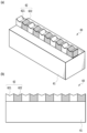
- FIG. 6 is a conceptual diagram showing the structure of the wavelength conversion element 60 according to the present disclosure, FIG. 6(a) showing a perspective view and FIG. 6(b) showing a front view.
- the wavelength conversion element 60 shown in the drawing includes a substrate 61 and a core 62 bonded on the substrate for wavelength conversion of incident light, like the wavelength conversion element 30 described above.
- the core 62 includes a positive core region 621 and a negative core region 622, and has a periodically poled structure in which the positive core region 621 and the negative core region 622 are periodically reversed with respect to the optical axis direction. have.
- FIG. 6 is a conceptual diagram showing the structure of the wavelength conversion element 60 according to the present disclosure, FIG. 6(a) showing a perspective view and FIG. 6(b) showing a front view.
- the wavelength conversion element 60 shown in the drawing includes a substrate 61 and a core 62 bonded on the substrate for wavelength conversion of incident light, like the wavelength conversion element 30 described above.
- the core 62 includes
- each of the positive core region 621 and the negative core region 622 has a maximum cross-sectional area at the end of each core region in the optical axis direction. It has a structure such that the cross-sectional area is the smallest in the central part of the direction.
- each core region has a constant width (the length in the direction perpendicular to the main surface of the substrate 61 and the direction perpendicular to the optical axis direction) and the height (the length in the direction perpendicular to the main surface of the substrate 61). direction length) decreases at a constant rate from one end to the center, and increases at a constant rate from the center to the other end.
- FIG. 7A and 7B are conceptual diagrams showing the structure of the wavelength conversion element 70 according to the present disclosure, where FIG. 7A is a perspective view, FIG. 7B is a top view, and FIG. 7C is a front view. ing.
- the wavelength conversion element 70 shown in the figure includes a substrate 71 and a core 72 bonded on the substrate for wavelength conversion of incident light, like the wavelength conversion elements 30 and 60 described above.
- the core 72 includes a positive core region 721 and a negative core region 722, and has a periodically poled structure in which the positive core region 721 and the negative core region 722 are periodically reversed with respect to the optical axis direction. have.
- each of the positive core region 721 and the negative core region 722 has a maximum cross-sectional area at the end of each core region in the optical axis direction.
- Each core region has a structure in which the cross-sectional area is minimized at the central portion in the optical axis direction.
- each core region has a width (the length in the direction perpendicular to the main surface of the substrate 71 and the direction perpendicular to the optical axis direction), and Both the height (the length in the direction perpendicular to the main surface of the substrate 71) decreases at a constant rate from one end toward the center, and at a constant rate from the center toward the other end. It has a structure that increases with
- FIG. 8 is a conceptual diagram showing the structure of the wavelength conversion element 80 according to the present disclosure, FIG. 8(a) showing a perspective view, and FIG. 8(b) showing a top view.
- the wavelength conversion element 80 shown in the figure includes a substrate 81 and a core 82 bonded on the substrate for wavelength conversion of incident light, like the wavelength conversion elements 30, 60 and 70 described above.
- the core 82 includes a positive core region 821 and a negative core region 822, and has a periodically poled structure in which the positive core region 821 and the negative core region 822 are periodically reversed with respect to the optical axis direction. have.
- FIG. 8 is a conceptual diagram showing the structure of the wavelength conversion element 80 according to the present disclosure, FIG. 8(a) showing a perspective view, and FIG. 8(b) showing a top view.
- the wavelength conversion element 80 shown in the figure includes a substrate 81 and a core 82 bonded on the substrate for wavelength conversion of incident light, like the wavelength conversion elements 30, 60 and 70 described above.
- each of the positive core region 821 and the negative core region 822 has a maximum cross-sectional area at the end of each core region in the optical axis direction. It has a structure such that the cross-sectional area is the smallest in the central part of the direction. However, unlike wavelength conversion elements 30, 60 and 70, the width of each core region varies (i.e., decreases and increases) asymmetrically in length from the centerline of the core region parallel to the optical axis direction. .
- wavelength conversion elements 60, 70 and 80 having such a configuration, similarly to the wavelength conversion element 30, it is possible to reduce the conversion efficiency of unintended wavelength conversion due to high-order quasi-phase matching. can be done.
- the wavelength conversion elements 60, 70 and 80 are structured such that the modulation curves from the ends to the center change linearly, they are not limited to this, as is the case with the wavelength conversion element 30.
- the change may have a curvature.
- each core region has a square or rectangular cross-sectional shape with respect to the optical axis direction, but is not limited to this.
- the cross-sectional shape of each core region with respect to the optical axis direction may be a trapezoid.
- the surface of each core region that is not bonded to the substrate may have a curvature.
- the wavelength conversion element according to the present disclosure has the effect of suppressing unintended high-order wavelength conversion as compared with the conventional technology. Therefore, since the desired wavelength conversion is performed more efficiently, it is expected to be applied to a laser light source used in fields such as optical communication and optical processing as a wavelength conversion element having higher efficiency than the conventional technology.
Landscapes
- Physics & Mathematics (AREA)
- Nonlinear Science (AREA)
- General Physics & Mathematics (AREA)
- Optics & Photonics (AREA)
- Chemical & Material Sciences (AREA)
- Crystallography & Structural Chemistry (AREA)
- Engineering & Computer Science (AREA)
- Ceramic Engineering (AREA)
- Optical Modulation, Optical Deflection, Nonlinear Optics, Optical Demodulation, Optical Logic Elements (AREA)
Priority Applications (3)
| Application Number | Priority Date | Filing Date | Title |
|---|---|---|---|
| US18/685,318 US20240353733A1 (en) | 2021-09-15 | 2021-09-15 | Wavelength Conversion Device |
| JP2023548012A JP7617478B2 (ja) | 2021-09-15 | 2021-09-15 | 波長変換素子 |
| PCT/JP2021/033985 WO2023042315A1 (ja) | 2021-09-15 | 2021-09-15 | 波長変換素子 |
Applications Claiming Priority (1)
| Application Number | Priority Date | Filing Date | Title |
|---|---|---|---|
| PCT/JP2021/033985 WO2023042315A1 (ja) | 2021-09-15 | 2021-09-15 | 波長変換素子 |
Publications (1)
| Publication Number | Publication Date |
|---|---|
| WO2023042315A1 true WO2023042315A1 (ja) | 2023-03-23 |
Family
ID=85602562
Family Applications (1)
| Application Number | Title | Priority Date | Filing Date |
|---|---|---|---|
| PCT/JP2021/033985 Ceased WO2023042315A1 (ja) | 2021-09-15 | 2021-09-15 | 波長変換素子 |
Country Status (3)
| Country | Link |
|---|---|
| US (1) | US20240353733A1 (https=) |
| JP (1) | JP7617478B2 (https=) |
| WO (1) | WO2023042315A1 (https=) |
Citations (8)
| Publication number | Priority date | Publication date | Assignee | Title |
|---|---|---|---|---|
| JPH06289448A (ja) * | 1993-04-02 | 1994-10-18 | Nippon Steel Corp | 第二高調波発生素子 |
| JPH08220578A (ja) * | 1994-08-31 | 1996-08-30 | Matsushita Electric Ind Co Ltd | 分極反転領域の製造方法ならびにそれを利用した光波長変換素子及びその製造方法 |
| JP2008310308A (ja) * | 2007-05-15 | 2008-12-25 | Panasonic Corp | レーザ波長変換装置、分極反転構造の形成方法及び画像表示装置 |
| JP2010197802A (ja) * | 2009-02-26 | 2010-09-09 | Nec Corp | 第二高調波発生素子及びその製造方法 |
| JP2011075604A (ja) * | 2009-09-29 | 2011-04-14 | Oki Electric Industry Co Ltd | 波長変換素子の製造方法 |
| JP2011257558A (ja) * | 2010-06-08 | 2011-12-22 | Nippon Telegr & Teleph Corp <Ntt> | 光学素子及びその製造方法 |
| WO2014030404A1 (ja) * | 2012-08-23 | 2014-02-27 | 日本碍子株式会社 | 波長変換素子 |
| WO2020100937A1 (ja) * | 2018-11-16 | 2020-05-22 | 日本電信電話株式会社 | 波長変換素子およびその作製方法 |
Family Cites Families (9)
| Publication number | Priority date | Publication date | Assignee | Title |
|---|---|---|---|---|
| DE69531917T2 (de) * | 1994-08-31 | 2004-08-19 | Matsushita Electric Industrial Co., Ltd., Kadoma | Verfahren zur Herstellung von invertierten Domänen und eines optischen Wellenlängenkonverters mit denselben |
| EP0782017B1 (en) * | 1995-12-28 | 2009-08-05 | Panasonic Corporation | Optical waveguide, optical wavelength conversion device, and methods for fabricating the same |
| US5875053A (en) * | 1996-01-26 | 1999-02-23 | Sdl, Inc. | Periodic electric field poled crystal waveguides |
| JP4514146B2 (ja) | 2005-05-30 | 2010-07-28 | 日本電信電話株式会社 | 周期分極反転光導波路素子の製造方法 |
| JP5168867B2 (ja) * | 2006-09-29 | 2013-03-27 | 沖電気工業株式会社 | 波長変換素子 |
| BRPI0901016A2 (pt) * | 2009-03-12 | 2009-11-17 | Navin Bhailalbhai Patel | dispositivo óptico não-linear usando materiais cúbicos não centrosimétricos para conversão de frequência |
| US8411353B2 (en) * | 2009-08-12 | 2013-04-02 | Polyvalor, Limited Partnerhsip | Quasi-phase-matched wavelength converter |
| US10114269B2 (en) | 2015-02-11 | 2018-10-30 | The Regents Of The University Of California | Heterogeneous waveguides and methods of manufacture |
| US20240152025A1 (en) * | 2021-04-12 | 2024-05-09 | Nippon Telegraph And Telephone Corporation | Optical Wavelength Conversion Device |
-
2021
- 2021-09-15 US US18/685,318 patent/US20240353733A1/en active Pending
- 2021-09-15 JP JP2023548012A patent/JP7617478B2/ja active Active
- 2021-09-15 WO PCT/JP2021/033985 patent/WO2023042315A1/ja not_active Ceased
Patent Citations (8)
| Publication number | Priority date | Publication date | Assignee | Title |
|---|---|---|---|---|
| JPH06289448A (ja) * | 1993-04-02 | 1994-10-18 | Nippon Steel Corp | 第二高調波発生素子 |
| JPH08220578A (ja) * | 1994-08-31 | 1996-08-30 | Matsushita Electric Ind Co Ltd | 分極反転領域の製造方法ならびにそれを利用した光波長変換素子及びその製造方法 |
| JP2008310308A (ja) * | 2007-05-15 | 2008-12-25 | Panasonic Corp | レーザ波長変換装置、分極反転構造の形成方法及び画像表示装置 |
| JP2010197802A (ja) * | 2009-02-26 | 2010-09-09 | Nec Corp | 第二高調波発生素子及びその製造方法 |
| JP2011075604A (ja) * | 2009-09-29 | 2011-04-14 | Oki Electric Industry Co Ltd | 波長変換素子の製造方法 |
| JP2011257558A (ja) * | 2010-06-08 | 2011-12-22 | Nippon Telegr & Teleph Corp <Ntt> | 光学素子及びその製造方法 |
| WO2014030404A1 (ja) * | 2012-08-23 | 2014-02-27 | 日本碍子株式会社 | 波長変換素子 |
| WO2020100937A1 (ja) * | 2018-11-16 | 2020-05-22 | 日本電信電話株式会社 | 波長変換素子およびその作製方法 |
Non-Patent Citations (3)
| Title |
|---|
| KURIMURA SUNAO, KATO YUJI, MARUYAMA MASAYUKI, USUI YUSUKE, NAKAJIMA HIROCHIKA: "Quasi-phase-matched adhered ridge waveguide in LiNbO3", APPLIED PHYSICS LETTERS, AMERICAN INSTITUTE OF PHYSICS, 2 HUNTINGTON QUADRANGLE, MELVILLE, NY 11747, vol. 89, no. 19, 9 November 2006 (2006-11-09), 2 Huntington Quadrangle, Melville, NY 11747, pages 191123 - 191123, XP012086834, ISSN: 0003-6951, DOI: 10.1063/1.2387940 * |
| RAO ASHUTOSH; CHILES JEFF; KHAN SAEED; TOROGHI SEYFOLLAH; MALINOWSKI MARCIN; CAMACHO-GONZáLEZ GUILLERMO FERNANDO; FATHPOUR SA: "Second-harmonic generation in single-mode integrated waveguides based on mode-shape modulation", APPLIED PHYSICS LETTERS, AMERICAN INSTITUTE OF PHYSICS, 2 HUNTINGTON QUADRANGLE, MELVILLE, NY 11747, vol. 110, no. 11, 17 March 2017 (2017-03-17), 2 Huntington Quadrangle, Melville, NY 11747, XP012217046, ISSN: 0003-6951, DOI: 10.1063/1.4978696 * |
| TAKESHI UMEKI ; OSAMU TADANAGA ; MASAKI ASOBE: "Highly Efficient Wavelength Converter Using Direct-Bonded PPZnLN Ridge Waveguide", IEEE JOURNAL OF QUANTUM ELECTRONICS, IEEE, USA, vol. 42, no. 8, 1 August 2010 (2010-08-01), USA, pages 1206 - 1213, XP011307330, ISSN: 0018-9197 * |
Also Published As
| Publication number | Publication date |
|---|---|
| US20240353733A1 (en) | 2024-10-24 |
| JP7617478B2 (ja) | 2025-01-20 |
| JPWO2023042315A1 (https=) | 2023-03-23 |
Similar Documents
| Publication | Publication Date | Title |
|---|---|---|
| JP7160194B2 (ja) | 波長変換素子 | |
| JPH05333395A (ja) | 光波長変換装置 | |
| JP2004219845A (ja) | 光導波路デバイスならびにそれを用いたコヒーレント光源およびそれを備えた光学装置 | |
| CN113540933A (zh) | 一种基于同步双光参量过程的中红外参量激光器 | |
| US11815785B2 (en) | Wavelength conversion optical element | |
| CN105264726B (zh) | 波导型激光装置 | |
| JP7473850B2 (ja) | 波長変換装置 | |
| JP7415195B2 (ja) | 波長変換素子 | |
| WO2023042315A1 (ja) | 波長変換素子 | |
| JP6348439B2 (ja) | 波長変換素子 | |
| WO2022219687A1 (ja) | 波長変換光学素子 | |
| JPH0651359A (ja) | 波長変換素子、短波長レーザ装置および波長可変レーザ装置 | |
| JP2643735B2 (ja) | 波長変換素子 | |
| JP2921208B2 (ja) | 波長変換素子および短波長レーザ光源 | |
| JP2007108593A (ja) | 非線形光学媒質およびそれを用いた波長変換装置 | |
| JP4877258B2 (ja) | 波長変換素子 | |
| JP7846421B2 (ja) | 波長変換素子の製造方法 | |
| JP2002250948A (ja) | 分極反転構造素子 | |
| JP2012118333A (ja) | 波長変換素子 | |
| JP2011033727A (ja) | 波長変換素子及び波長変換光源 | |
| JP2008089762A (ja) | 波長変換素子および波長変換装置 | |
| JP2015215501A (ja) | 波長変換素子 | |
| JP2007322695A (ja) | 波長変換素子 | |
| JP2007187920A (ja) | 非線形光学媒質およびそれを用いた波長変換装置 | |
| JP6018525B2 (ja) | 波長変換素子および波長変換装置 |
Legal Events
| Date | Code | Title | Description |
|---|---|---|---|
| 121 | Ep: the epo has been informed by wipo that ep was designated in this application |
Ref document number: 21957497 Country of ref document: EP Kind code of ref document: A1 |
|
| WWE | Wipo information: entry into national phase |
Ref document number: 2023548012 Country of ref document: JP |
|
| WWE | Wipo information: entry into national phase |
Ref document number: 18685318 Country of ref document: US |
|
| NENP | Non-entry into the national phase |
Ref country code: DE |
|
| 122 | Ep: pct application non-entry in european phase |
Ref document number: 21957497 Country of ref document: EP Kind code of ref document: A1 |