WO2023037913A1 - コンデンサ装置 - Google Patents
コンデンサ装置 Download PDFInfo
- Publication number
- WO2023037913A1 WO2023037913A1 PCT/JP2022/032311 JP2022032311W WO2023037913A1 WO 2023037913 A1 WO2023037913 A1 WO 2023037913A1 JP 2022032311 W JP2022032311 W JP 2022032311W WO 2023037913 A1 WO2023037913 A1 WO 2023037913A1
- Authority
- WO
- WIPO (PCT)
- Prior art keywords
- terminal
- capacitor
- cathode
- anode
- connection lead
- Prior art date
Links
- 239000003990 capacitor Substances 0.000 title claims abstract description 209
- 230000008093 supporting effect Effects 0.000 claims description 44
- 239000011347 resin Substances 0.000 claims description 39
- 229920005989 resin Polymers 0.000 claims description 39
- 239000000463 material Substances 0.000 claims description 29
- 239000003792 electrolyte Substances 0.000 description 11
- 239000007787 solid Substances 0.000 description 10
- 239000007788 liquid Substances 0.000 description 9
- 238000004519 manufacturing process Methods 0.000 description 9
- 238000000465 moulding Methods 0.000 description 9
- 239000007784 solid electrolyte Substances 0.000 description 9
- 239000000126 substance Substances 0.000 description 7
- 230000002093 peripheral effect Effects 0.000 description 5
- 230000000694 effects Effects 0.000 description 4
- 229910052751 metal Inorganic materials 0.000 description 4
- 239000002184 metal Substances 0.000 description 4
- 238000000034 method Methods 0.000 description 4
- 230000004048 modification Effects 0.000 description 4
- 238000012986 modification Methods 0.000 description 4
- 238000003466 welding Methods 0.000 description 4
- 230000008901 benefit Effects 0.000 description 3
- 230000008569 process Effects 0.000 description 3
- 230000035882 stress Effects 0.000 description 3
- 229910052782 aluminium Inorganic materials 0.000 description 2
- XAGFODPZIPBFFR-UHFFFAOYSA-N aluminium Chemical compound [Al] XAGFODPZIPBFFR-UHFFFAOYSA-N 0.000 description 2
- 239000010406 cathode material Substances 0.000 description 2
- 238000006243 chemical reaction Methods 0.000 description 2
- 239000008151 electrolyte solution Substances 0.000 description 2
- 238000005530 etching Methods 0.000 description 2
- 230000020169 heat generation Effects 0.000 description 2
- 230000010354 integration Effects 0.000 description 2
- 238000004080 punching Methods 0.000 description 2
- 230000006641 stabilisation Effects 0.000 description 2
- 238000011105 stabilization Methods 0.000 description 2
- QNRATNLHPGXHMA-XZHTYLCXSA-N (r)-(6-ethoxyquinolin-4-yl)-[(2s,4s,5r)-5-ethyl-1-azabicyclo[2.2.2]octan-2-yl]methanol;hydrochloride Chemical compound Cl.C([C@H]([C@H](C1)CC)C2)CN1[C@@H]2[C@H](O)C1=CC=NC2=CC=C(OCC)C=C21 QNRATNLHPGXHMA-XZHTYLCXSA-N 0.000 description 1
- OKTJSMMVPCPJKN-UHFFFAOYSA-N Carbon Chemical compound [C] OKTJSMMVPCPJKN-UHFFFAOYSA-N 0.000 description 1
- VYZAMTAEIAYCRO-UHFFFAOYSA-N Chromium Chemical compound [Cr] VYZAMTAEIAYCRO-UHFFFAOYSA-N 0.000 description 1
- BQCADISMDOOEFD-UHFFFAOYSA-N Silver Chemical compound [Ag] BQCADISMDOOEFD-UHFFFAOYSA-N 0.000 description 1
- RTAQQCXQSZGOHL-UHFFFAOYSA-N Titanium Chemical compound [Ti] RTAQQCXQSZGOHL-UHFFFAOYSA-N 0.000 description 1
- HCHKCACWOHOZIP-UHFFFAOYSA-N Zinc Chemical compound [Zn] HCHKCACWOHOZIP-UHFFFAOYSA-N 0.000 description 1
- 230000009471 action Effects 0.000 description 1
- 239000000853 adhesive Substances 0.000 description 1
- 230000001070 adhesive effect Effects 0.000 description 1
- 230000002411 adverse Effects 0.000 description 1
- 238000004873 anchoring Methods 0.000 description 1
- 238000007743 anodising Methods 0.000 description 1
- 229910052799 carbon Inorganic materials 0.000 description 1
- 230000008859 change Effects 0.000 description 1
- 229910052804 chromium Inorganic materials 0.000 description 1
- 239000011651 chromium Substances 0.000 description 1
- 239000011248 coating agent Substances 0.000 description 1
- 238000000576 coating method Methods 0.000 description 1
- 150000001875 compounds Chemical class 0.000 description 1
- 229920001940 conductive polymer Polymers 0.000 description 1
- 239000004020 conductor Substances 0.000 description 1
- 230000007547 defect Effects 0.000 description 1
- 230000008021 deposition Effects 0.000 description 1
- 230000006866 deterioration Effects 0.000 description 1
- 238000010586 diagram Methods 0.000 description 1
- 238000009499 grossing Methods 0.000 description 1
- 238000010438 heat treatment Methods 0.000 description 1
- 238000005304 joining Methods 0.000 description 1
- 238000010030 laminating Methods 0.000 description 1
- 150000002739 metals Chemical class 0.000 description 1
- 229910052758 niobium Inorganic materials 0.000 description 1
- 239000010955 niobium Substances 0.000 description 1
- GUCVJGMIXFAOAE-UHFFFAOYSA-N niobium atom Chemical compound [Nb] GUCVJGMIXFAOAE-UHFFFAOYSA-N 0.000 description 1
- 230000003647 oxidation Effects 0.000 description 1
- 238000007254 oxidation reaction Methods 0.000 description 1
- 239000002245 particle Substances 0.000 description 1
- 238000003825 pressing Methods 0.000 description 1
- 230000009467 reduction Effects 0.000 description 1
- 238000000926 separation method Methods 0.000 description 1
- 238000004904 shortening Methods 0.000 description 1
- 229910052709 silver Inorganic materials 0.000 description 1
- 239000004332 silver Substances 0.000 description 1
- 229910000679 solder Inorganic materials 0.000 description 1
- 230000000087 stabilizing effect Effects 0.000 description 1
- 229910052715 tantalum Inorganic materials 0.000 description 1
- GUVRBAGPIYLISA-UHFFFAOYSA-N tantalum atom Chemical compound [Ta] GUVRBAGPIYLISA-UHFFFAOYSA-N 0.000 description 1
- 230000008646 thermal stress Effects 0.000 description 1
- 229910052719 titanium Inorganic materials 0.000 description 1
- 239000010936 titanium Substances 0.000 description 1
- 229910052725 zinc Inorganic materials 0.000 description 1
- 239000011701 zinc Substances 0.000 description 1
Images


Classifications
-
- H—ELECTRICITY
- H01—ELECTRIC ELEMENTS
- H01G—CAPACITORS; CAPACITORS, RECTIFIERS, DETECTORS, SWITCHING DEVICES OR LIGHT-SENSITIVE DEVICES, OF THE ELECTROLYTIC TYPE
- H01G4/00—Fixed capacitors; Processes of their manufacture
- H01G4/002—Details
- H01G4/228—Terminals
-
- H—ELECTRICITY
- H01—ELECTRIC ELEMENTS
- H01G—CAPACITORS; CAPACITORS, RECTIFIERS, DETECTORS, SWITCHING DEVICES OR LIGHT-SENSITIVE DEVICES, OF THE ELECTROLYTIC TYPE
- H01G4/00—Fixed capacitors; Processes of their manufacture
- H01G4/38—Multiple capacitors, i.e. structural combinations of fixed capacitors
-
- H—ELECTRICITY
- H01—ELECTRIC ELEMENTS
- H01G—CAPACITORS; CAPACITORS, RECTIFIERS, DETECTORS, SWITCHING DEVICES OR LIGHT-SENSITIVE DEVICES, OF THE ELECTROLYTIC TYPE
- H01G9/00—Electrolytic capacitors, rectifiers, detectors, switching devices, light-sensitive or temperature-sensitive devices; Processes of their manufacture
- H01G9/004—Details
- H01G9/008—Terminals
- H01G9/012—Terminals specially adapted for solid capacitors
-
- H—ELECTRICITY
- H01—ELECTRIC ELEMENTS
- H01G—CAPACITORS; CAPACITORS, RECTIFIERS, DETECTORS, SWITCHING DEVICES OR LIGHT-SENSITIVE DEVICES, OF THE ELECTROLYTIC TYPE
- H01G9/00—Electrolytic capacitors, rectifiers, detectors, switching devices, light-sensitive or temperature-sensitive devices; Processes of their manufacture
- H01G9/15—Solid electrolytic capacitors
Definitions
- the present invention relates to capacitor devices.
- electrolytic capacitors such as aluminum electrolytic capacitors have been widely used as capacitors in various circuits. Reduction and increase in capacity are desired. In particular, in applications in circuits where high ripple current occurs, internal heat generation due to ESR shortens the product life of the capacitor. Capacitors are increasingly used.
- chip-type solid electrolytic capacitors are known in which a plurality of capacitor elements are conductively connected in parallel to a lead frame and formed by resin molding (see, for example, the following patent documents: 1). With such a configuration, it is possible to increase the capacity and reduce the ESR.
- the present invention solves the above problems, and its object is to realize a capacitor device capable of improving reliability while ensuring the characteristics of large capacity and low ESR.
- a capacitor device comprises a laminated anode, an insulating film and a cathode, an anode terminal portion electrically connected to the anode and exposed to the outside, and an anode terminal portion electrically connected to the cathode.
- a plurality of capacitor elements having cathode terminal portions exposed to the outside; an anode connection lead portion conductively connected commonly to the anode terminal portions of the plurality of capacitor elements; and the cathodes of the plurality of capacitor elements.
- the plurality of capacitor elements and the anode connection are exposed in a state in which the cathode connection lead portion conductively connected in common to the terminal portion, the electrode portion of the anode connection lead portion, and the electrode portion of the cathode connection lead portion are exposed. and a resin material encasing the assembly of the lead and the cathode connection lead.
- the plurality of capacitor elements are arranged so that the respective anode terminal portions and cathode terminal portions are arranged in parallel with each other.
- a terminal support portion provided in the anode connection lead portion or the cathode connection lead portion for supporting and conductively connecting the anode terminal portion or the cathode terminal portion of the capacitor element;
- a terminal holding portion is provided on the cathode connection lead portion to hold and electrically connect the anode terminal portion or the cathode terminal portion of the capacitor element.
- the terminal holding portion extends from the side edge of the terminal supporting portion in the parallel direction of the plurality of capacitor elements.
- the terminal holding portion in both the anode connection lead portion and the cathode connection lead portion, the terminal holding portion preferably extends from the side edge of the terminal support portion in the parallel direction of the plurality of capacitor elements.
- the terminal holding portion bends or bends from the side edge of the terminal supporting portion and then extends in the parallel direction to hold a plurality of parallel capacitor elements.
- the terminal holding portion hold the capacitor element from the side opposite to the side where the capacitor element is supported by the terminal support portion.
- the terminal holding portion in both the anode connection lead portion and the cathode connection lead portion, the terminal holding portion preferably holds the capacitor element from the side opposite to the side of the capacitor element supported by the terminal support portion.
- the anode terminal portion protrudes and is exposed in the axial direction from a rod-shaped body portion in which the anode, the insulating coating, and the cathode are coaxially laminated, and the cathode terminal portion is: It is preferable to expose to the outer peripheral surface of the said main-body part.
- the anode connection lead portion or the cathode connection lead portion has a step formed so that the terminal support portion is arranged inside the resin material while being shifted toward the inside of the resin material with respect to the electrode portion. It is preferable to have At this time, it is desirable that both the anode connection lead portion and the cathode connection lead portion have the step.
- the plurality of capacitor elements be arranged on the terminal supporting portion in a manner of being stacked in a plurality of stages.
- a plurality of terminal holding portions are provided for respectively holding the capacitor elements in different stages of the plurality of stages.
- the plurality of capacitor elements include the capacitor element having a size or shape different from that of the other capacitor elements.
- the anode connection lead portion or the cathode connection lead portion is provided in a state in which the anode terminal portion or the cathode terminal portion of the plurality of capacitor elements and the anode connection lead portion or the cathode connection lead portion are electrically connected to each other.
- the terminal supporting portion and the terminal holding portion support and hold the anode terminal portion or the cathode terminal portion of the capacitor element, and are conductively connected.
- the contact area of the conductive connection portion of the assembly in which a plurality of capacitor elements are connected in parallel is increased, the resistance is reduced, and the conductive connection portion is stabilized, thereby increasing the capacity of the capacitor device. Reliability can be improved while ensuring low ESR characteristics.
- the terminal holding portion extends from the side edge of the terminal supporting portion in the parallel direction of the plurality of capacitor elements, the plurality of capacitor elements can be reliably and easily attached to the anode connection lead portion and the cathode connection lead portion. Since it can be integrated in a conductive connection state, it is possible to improve reliability and productivity.
- the integrity of the assembly formed by connecting a plurality of capacitor elements in parallel is further improved, so that the conductive connection portion can be easily connected.
- Reliability is further improved by stabilization, and productivity can be improved by improving the efficiency of assembly work in the manufacturing process and facilitating the conductive connection work.
- FIG. 3A to 3D are perspective views showing examples of the shape of a capacitor element constituting an embodiment of a capacitor device according to the present invention.
- FIG. It is an anode side end view (a), an internal cross-sectional view (b), and a cathode side end view (c) of one example of the capacitor element of the same embodiment.
- It is a longitudinal cross-sectional view of the body portion of the capacitor element of the same embodiment.
- FIG. 3 is an enlarged cross-sectional view schematically showing the peripheral structure of the insulating film of the capacitor element of the same embodiment.
- It is the top view (a) and partial side view (b) which show typically the structural example of the lead frame used for the 1st Example of the capacitor
- FIG. 3A is a cross-sectional view (a) and a vertical cross-sectional view (b) schematically showing the internal structure after resin molding of the first example of the capacitor device of the same embodiment. It is the top view (a) and front view (b) which show typically the structure before the resin molding of 2nd Example of the same embodiment. It is the top view (a) and front view (b) which show typically the structure before resin molding of 3rd Example of the same embodiment.
- FIG. 10A to 10C are front views schematically showing an example of a conductive connection structure for connecting the anode connection lead portion to the anode terminal portion or the cathode connection lead portion to the cathode terminal portion in each example of the same embodiment.
- FIG. FIG. 4 is a schematic explanatory cross-sectional view for explaining a manufacturing process of a capacitor element;
- FIGS. 1 to 4 the configuration of a capacitor element that constitutes a capacitor device according to the present invention will be described.
- FIG. 1 is perspective views (a) to (d) schematically showing an example of the appearance of a capacitor element 10.
- a main body portion 10B having a capacitor function is configured in a bar shape, a shaft-shaped anode terminal portion 11T protrudes in the axial direction from the center of the end portion of the main body portion 10B, and the outer peripheral surface of the main body portion 10B is A cathode terminal portion 14T is formed.
- the body portion 10B has a cylindrical shape
- the anode terminal portion 11T has a cylindrical shape with a diameter smaller than that of the body portion 10B.
- the body portion 10B has a cylindrical shape
- the anode terminal portion 11T' has a prism shape (square prism shape, plate shape) having a smaller cross-sectional area than the body portion 10B.
- the main body portion 10B' is prismatic (square prismatic)
- the anode terminal portion 11T is cylindrical with a smaller cross-sectional area than the main body portion 10B'.
- the main body portion 10B' is prismatic (square prismatic)
- the anode terminal portion 11T' is prismatic (square prismatic, plate-like) smaller than the main body portion 10B.
- All of these capacitor elements 10 are rod-shaped as a whole, and as shown in FIG. 2, have a long (extended) shape in the axial direction.
- the body portion 10B has a capacitor function, and one terminal portion (anode terminal portions 11T and 11T') has a shape protruding from the body portions 10B and 10B' in the axial direction. Also, the terminal portions 11T and 11T' have a smaller cross-sectional shape than the body portions 10B and 10B'.
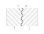
- the capacitor element 10 is configured by coaxially laminating an anode 11, an insulating film 12, an electrolyte part 13, and a cathode 14 from the center in a body part 10B.
- Anode 11 is preferably made of a valve metal such as aluminum, tantalum, chromium, titanium, zinc or niobium.
- the insulating film 12 is preferably composed of an anodized film of these valve metals.
- the surface of the anode 11 is subjected to surface enlarging treatment such as etching to increase the surface area, and the insulating film 12 made of an anodized film formed by chemical conversion treatment is formed on the treated surface.
- an electrolyte part 13 composed of a solid electrolyte, a solid electrolyte and a drive electrolyte, or a solid electrolyte and a functional liquid substance is formed.
- the electrolyte part 13 may exist in layers when it is composed only of a solid electrolyte.
- the electrolyte portion 13 contains a solid electrolyte and a liquid substance, for example, the solid electrolyte portion can be a particulate conductive polymer compound, and the particles aggregate to form a solid electrolyte phase.
- a liquid substance such as a driving electrolyte or a functional liquid substance exists so as to surround the solid electrolyte phase, and can form a liquid substance phase.
- the ESR equivalent series resistance
- the device 1 as a whole can also be characterized by low ESR.
- the cathode 14 provided on the outer periphery of the electrolyte part 13 is not particularly limited, but can be made of, for example, a conductive paste such as carbon paste. Moreover, it is desirable to form a cathode terminal portion 14T made of a conductive paste such as silver paste on the outer peripheral surface of the cathode 14 .
- the cathode terminal portion 14T may be provided integrally with the cathode 14 (or made of the same material) as shown in FIG. 2(b).
- the plurality of anodes 11 are arranged in a parallel posture with a space therebetween in such a manner that the portion to be the anode terminal portion 11T is held by a connecting member 60.
- an etching process surface enlarging treatment
- a chemical conversion process anodic oxidation treatment
- an electrolyte adhesion process an electrolyte adhesion process
- a cathode material conductive paste
- the connecting member 60 is preferably made of a conductive material electrically connected to the anode 11 .
- the electrolyte portion 13, the cathode 14, and the cathode terminal portion 14T can be sequentially formed by immersing in the treatment liquid in the treatment tank. In this way, a plurality of capacitor elements 10 can be manufactured in parallel, and production efficiency can be improved.
- FIG. 5(a) is an enlarged plan view showing a region of the lead frame 50 to be the anode connection lead portion 2 and the cathode connection lead portion 3 of the capacitor device 1
- FIG. 3B is a side view (b) of a portion to be a cathode connection lead portion 3.
- the lead frame 50 is formed of a metal plate that is progressively processed by a press machine or the like, and is formed by punching the metal plate.
- the lead frame 50 has an anode connection region portion 51 protruding like a peninsula into the punched region 50a, and a peninsular shape protruded into the punched region 50a in a direction opposite to the anode connection region 51, and is separated from the anode connection region 51. and a cathode connection region portion 52 configured to face each other across the .
- the anode connection region portion 51 includes a base portion 51a, a head portion 51b provided at the tip of the base portion 51a, and an extension portion 51c extending from the head portion 51b in a direction (lateral side in the drawing) different from the projecting direction. , provided.
- the cathode connection region 52 includes a base portion 52a, a head portion 52b provided at the tip of the base portion 52a, and an extension portion 52c further extending from the head portion 52b in the different direction (side in the drawing).
- a pair of extending portions 51c and 52c extending from left and right side edges of the head portions 51b and 52b are provided.
- the head portion 51b is bent or bent with respect to the base portion 51a so as to have a step 51s in the thickness direction of the lead frame 50.
- the cathode connection region portion 52 is also bent or bent so that the head portion 52b has a step 52s in the thickness direction of the lead frame 50 with respect to the base portion 52a.
- the shape of these steps 51s and 52s can be formed by pressing the lead frame 50. As shown in FIG.
- FIG. 1A and 1B are a plan view (a) and a front view (b) showing an assembly 1A conductively connected to an anode connection lead portion 2 and a cathode connection lead portion 3 which are separated from each other.
- the anode connection lead portion 2 includes an electrode portion 2a formed of at least a portion of the base portion 51a of the anode connection region portion 51, a terminal support portion 2b formed of the head portion 51b, and a terminal holding portion 2c formed of the extension portion 51c.
- the cathode connection lead portion 3 includes an electrode portion 3a formed of at least a part of the base portion 52a of the cathode connection region portion 52, a terminal support portion 3b formed of the head portion 52b, and a terminal holding portion formed of the extension portion 52c. and a portion 3c.
- the plurality of capacitor elements 10 are arranged in parallel with each other in the same (parallel) posture in which the anode terminal portion 11T is arranged on the terminal support portion 2b and the main body portion 10B is arranged on the terminal support portion 3b. aligned to In this first embodiment, a plurality of capacitor elements 10 are arranged in a line on the terminal support portions 2b and 3b.
- the terminal holding portions 2c and 3c protruding from the side edges of the terminal supporting portions 2b and 3b are bent or bent to extend in the parallel direction of the plurality of capacitor elements 10, and the anode terminal portion 11T and the main body portion extend. It is in contact with 10B so as to cover it from above.
- the anode terminal portion 11T is held between the terminal support portion 2b and the terminal holding portion 2c
- the cathode terminal portion 14T is held between the terminal support portion 3b and the terminal holding portion 3c. be. That is, both the anode terminal portion 11T and the cathode terminal portion 14T are supported and held from opposite sides by the terminal supporting portions 2b, 3b and the terminal holding portions 2c, 3c. This reduces the load when the conductive connection portions between the anode terminal portion 11T and the cathode terminal portion 14T and the anode connection lead portion 2 and the cathode connection lead portion 3 receive an external force. Since separation is suppressed, electrical reliability can be improved.
- a pair of terminal holding portions 2c and 3c extend to the left and right sides of the terminal supporting portions 2b and 3b, respectively.
- a part of the plurality of capacitor elements 10 and the rest thereof are shared from the left and right, respectively, and are configured to be held from above.
- the tip portions of the left and right terminal holding portions 2c and 3c may be connected to each other by some member or joining method.
- both the anode terminal portion 11T and the cathode terminal portion 14T are conductively connected to the terminal supporting portions 2b, 3b and the terminal holding portions 2c, 3c at the supporting portions and the holding portions.
- the anode terminal portion 11T is preferably welded to the terminal support portion 2b and the terminal holding portion 2c by laser welding or resistance welding. It is preferable to use a conductive adhesive that can be bonded at a low temperature such as a conductive paste. This is because the life of the capacitor element 10 may be shortened by heating the body portion 10B of the capacitor element 10 when conductively connecting the cathode terminal portion 14T.
- connection resistance of the conductive connection portion can be reduced when the conductive connection mode is welding. Welding also improves the reliability of the conductive connection.
- the form of the conductive connection itself is not particularly limited as long as there is no problem.
- the conductive connections between the terminal supporting portions 2b and 3b and the terminal holding portions 2c and 3c and the anode terminal portion 11T and the cathode terminal portion 14T are the supporting portions of the terminal supporting portions 2b and 3b and the terminal holding portion 2c. , 3c. Therefore, the increase in the number of conductive connection points increases the overall conductive connection area, and the junction resistance of the parallel connection structure of the plurality of capacitor elements 10 can be reduced. Further, by making the surface shape of the holding portions of the terminal holding portions 2c and 3c conform to the surface of the cathode terminal portion 14T, the conductive connection area can be further increased.
- the cathode terminal portions 14T between the adjacent capacitor elements 10 are not in contact with each other (main body portion 10B.), but unlike the illustrated example, by bringing the body portions 10B into contact with each other, the conductive connection area between the plurality of capacitor elements 10 can be increased, and the assembly 1A Compactness can be achieved.
- FIG. 7 shows a cross-sectional view (a) and a vertical cross-sectional view (b) when the capacitor device 1 is formed by molding the assembly 1A with (insulating) resin and enclosing it with the resin material 4.
- FIG. 7 shows a cross-sectional view (a) and a vertical cross-sectional view (b) when the capacitor device 1 is formed by molding the assembly 1A with (insulating) resin and enclosing it with the resin material 4.
- FIG. 7 shows a cross-sectional view (a) and a vertical cross-sectional view (b) when the capacitor device 1 is formed by molding the assembly 1A with (insulating) resin and enclosing it with the resin material 4.
- FIG. 7 shows a cross-sectional view (a) and a vertical cross-sectional view (b) when the capacitor device 1 is formed by molding the assembly 1A with (insulating) resin and enclosing it with the resin material 4.
- FIG. 7 shows a cross-sectional view (a) and a vertical
- the assembly 1A in which a plurality of capacitor elements 10 are held by the terminal supporting portions 2b, 3b and the terminal holding portions 2c, 3c and are conductively connected is covered by the resin material 4. Therefore, the rigidity of the assembly 1A is further improved. For this reason, even if the device is subjected to thermal stress such as solder reflow during mounting on the circuit board or mechanical stress received from the circuit board after mounting, the possibility of defects occurring can be reduced, thereby increasing reliability. improve sexuality.
- the resin material 4 includes the terminal supporting portions 2b and 3b which are arranged inside the electrode portions 2a and 3a with steps 2s and 3s from both upper and lower sides of the drawing, the anode connecting lead portion 2 and the cathode Since the bonding force between the connection lead portion 3 and the resin material 4 can be increased, there is almost no need to change the basic structure of the anode connection lead portion 2 and the cathode connection lead portion 3, and furthermore, without sacrificing compactness, Product reliability can be further enhanced.
- the step amounts of the steps 2s and 3s are set so that the terminal support portions 2b and 3b can support (abut on) the anode terminal portion 11T and the cathode terminal portion 14T.
- the electrode portion 2a of the anode connection lead portion 2 and the electrode portion 3a of the cathode connection lead portion 3 are set at the same height.
- the configuration is basically similar to that of the first embodiment described above, but the terminal holding portions 2c and 3c each extend only from one side of the terminal supporting portions 2b and 3b.
- Each terminal holding portion 2c, 3c is folded back from one side to the other side to hold all the plurality of capacitor elements 10 arranged side by side from above. ing. Even with this configuration, the same effects as in the first embodiment can be obtained.
- the tip portions of the terminal holding portions 2c and 3c are separated from the terminal support portions 2b and 3b, but the tip portions of the terminal holding portions 2c and 3c are folded back from one side to the other side. Later, the other side may be configured to be mechanically and electrically connected to the terminal supporting portions 2b and 3b. Also, in the second embodiment, as long as there is no problem, the configuration can be the same as each point explained in the first embodiment, but the explanation thereof will be omitted.
- a third embodiment of the present invention will be described.
- a plurality of capacitor elements 10 are arranged in two stages on the terminal supporting portions 2b and 3b. That is, some of the plurality of capacitor elements 10 are arranged on the terminal support portions 2b and 3b, but the remaining plurality of capacitor elements 10 are the already arranged part of the plurality of capacitor elements 10. is mounted on an array of a plurality of capacitor elements 10 of Although the plurality of capacitor elements 10 are mounted in two stages in the illustrated example, they may be mounted in three or more stages. Also, the number of capacitor elements 10 arranged in each stage is not particularly limited, and may be the same number as the other stages as shown in the figure, or may be a different number.
- a plurality of terminal holding portions 2c, 3c extend from the terminal supporting portions 2b, 3b, and different terminal holding portions 2c, 3c are connected to the capacitor elements 10 at respective stages of the capacitor elements 10 at a plurality of stages. is configured to hold In the illustrated example, a plurality (two) of terminal holding portions 2c and 3c extend from different locations in the vertical direction of the drawing on the left and right side edges of the terminal supporting portions 2b and 3b. It holds a plurality of capacitor elements 10 respectively.
- the capacitor elements 10 mounted in a plurality of stages can be stably and reliably held in each stage.
- the terminal holding portions 2c and 3c are provided to hold the respective stages of the plurality of capacitor elements 10 mounted in a plurality of stages. It may be held by holding portions 2c and 3c.
- a terminal supporting portion 2d indicated by a dotted line in FIG. 9 supports the anode terminal portion 11T on the second stage (and thereafter).
- This terminal support portion 2d is also preferably conductively connected to the anode terminal portion 11T.
- the capacitor elements 10 in the second stage (or later) are arranged to be shifted in the axial direction with respect to the first stage, and a terminal support portion 3d (not shown) for supporting the cathode terminal portion 14T is provided.
- the terminal holding portion 3c on the first stage often ends up supporting the cathode terminal portion 14T on the second stage (and thereafter) as shown in the illustrated example, only the terminal holding portion 3c is provided. Therefore, the terminal support portion 3d may not be provided.
- the third embodiment can be constructed in the same manner as the points explained in the first or second embodiment as long as there is no problem, but the explanation thereof will be omitted.
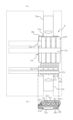
- FIG. 10 is a cross-sectional view (a) and a vertical cross-sectional view (b) showing the structure of the capacitor device 1 of this embodiment.
- the conductive connection structure can be maintained by the binding force of the resin material 4.
- FIG. 10 since a plurality of capacitor elements 10 are mounted on the terminal supporting portions 2b and 3b in a plurality of stages, the degree of integration of the capacitor elements 10 can be further increased and the adjacent capacitors
- the resin material 4 is interposed between the elements 10 not only in the planar direction but also in the vertical direction.
- the rigidity of the assembly can be further increased by bonding to the . Therefore, even though a larger number of capacitor elements 10 are connected in parallel, reliability can be easily ensured, and the manufacturing work can be simplified, thereby improving productivity.
- a plurality of capacitor elements 10 stacked in a plurality of stages
- it may be configured to hold a part and the remaining capacitor elements 10 in the same stage, Alternatively, the same plurality of capacitor elements 10 may be held at a plurality of locations by a plurality of terminal holding portions 2c and 3c.
- FIG. 11 shows the structure of an assembly 1A of a plurality of capacitor elements 10, an anode connection lead portion 2 and a cathode connection lead portion 3 in the fourth embodiment.
- This embodiment includes a plurality of capacitor elements 10 mounted in a plurality of stages on the terminal support portions 2b and 3b in the same manner as in the third embodiment. It is different from the third embodiment in that it does not extend from both side edges, but only from one side edge. However, a plurality of terminal holding portions 2c and 3c extending from different positions in the vertical direction of the drawing among the side edges of the terminal supporting portions 2b and 3b correspond to the arrangement of the capacitor elements 10 in a plurality of stages. , is the same as the third embodiment.
- the tip portions of the terminal holding portions 2c and 3c folded back from one side to the other side are separated from the terminal support portions 2b and 3b in the illustrated example, but the tip portions of the terminal holding portions 2c and 3c are separated from each other. After folding from one side to the other side, the other side may be mechanically and electrically connected to the terminal supporting portions 2b and 3b.
- a plurality of terminal holding portions 2c and 3c corresponding to each stage are extended from both side edges of the terminal support portions 2b and 3b, respectively, and are folded back to opposite sides to form capacitor elements 10 in different stages. may be held.
- the fourth embodiment can be constructed in the same manner as the points described in any of the first to third embodiments as long as there is no problem, but the description thereof will be omitted.
- a step 3t is formed in a portion of the cathode connection lead portion 3, in the illustrated example, in a portion adjacent to the terminal support portion 3b. is not embedded in the resin material 4 and is configured to be the electrode portion 3 e exposed from the resin material 4 .
- the capacitor device 1 can be used as a three-terminal capacitor provided with the electrode portion 3e in addition to the electrode portions 2a and 3a.
- the terminal support portions 2b, 3b are displaced inside the resin material 4 with respect to the electrode portions 2a, 3a, 3e due to the presence of the steps 2s, 3s, 3t. Therefore, the bonding area with the resin material 4 can be increased without substantially changing the basic structure of the lead portions 2 and 3 and without sacrificing the compactness of the capacitor device 1. . Therefore, the bonding force between the assembly 1A and the resin material 4 can be increased.
- the fifth embodiment can also be configured in the same manner as the points described in the first to fourth embodiments as long as there is no problem, but the description thereof will be omitted.
- FIG. 13 is an explanatory diagram showing modifications (a) to (c) that can be used in each of the above embodiments.
- Each characteristic configuration of each example of the above-described embodiments can be appropriately replaced with another configuration or arbitrarily combined with each other as long as there is no mutual problem.
- 13(a) to 13(c) can also be appropriately replaced with other configurations or arbitrarily combined with each other as long as they do not interfere with each other. be able to.
- 13A to 13C for convenience of explanation, only one of the terminal supporting portion 2b and the terminal holding portion 2c and the terminal supporting portion 3b and the terminal holding portion 3c is shown, and the other is shown. are omitted.
- the plurality of capacitor elements 10 are provided with an anode terminal portion 11T' having a rectangular cross section or plate shape.
- the terminal supporting portion 2b supports the anode terminal portion 11T'
- the terminal holding portion 2c holds the anode terminal portion 11T'.
- the contact area between the terminal supporting portion 2b and the terminal holding portion 2c can be increased by the anode terminal portion 11T' having a rectangular or plate-like cross section. Since the electrical resistance value of the portion can be further reduced, the reliability can be further improved.
- the plurality of capacitor elements 10 has a main body portion 10B' having a rectangular or prismatic cross section.
- the cathode terminal portion 14T' has a flat portion, it is possible to increase the contact area with the terminal support portion 3b and the terminal holding portion 3c, so that the stability of the assembly is further improved and the bonding is improved. Since the electrical resistance value of the portion can be further reduced, the reliability can be further improved.
- the plurality of capacitor elements include capacitor elements 10 and 10′′ having mutually different dimensions and shapes.
- the element 10 and the capacitor element 10'' having a small outer diameter of the main body portion 10B'' are mixed. In this way, by appropriately combining and assembling the capacitor elements having mutually different dimensions and shapes, high density can be achieved.
- the size of the capacitor element is not particularly limited, but the main body
- the outer diameter of the cross section or the width of one side is preferably within the range of 0.1-10.0 mm, preferably within the range of 0.3-3.0 mm.
- the outer diameter of the main body part 10B is 0.9 mm
- the outer diameter of the body portion 10B'' is 0.5 mm.
- the types of capacitor device 1 can be diversified.
- capacitor elements having mutually different shapes such as a rectangular cross-sectional shape and a rhombic cross-sectional shape may be included.
- the capacitance and rated voltage of the capacitor element may differ from each other.
- a smoothing capacitor When a smoothing capacitor is used in a rectifier circuit, etc., it is necessary to use a capacitor that satisfies a predetermined condition with respect to ripple current, thereby preventing internal heat generation of the used capacitor and avoiding shortening of the life of the capacitor. can be done.
- a combination of a plurality of capacitors may be used in order to reduce the parts cost while satisfying the above conditions.
- the parts cost can be further reduced by making the plurality of capacitors used in combination have mutually different performances. Therefore, as in the example shown in FIG. 13C, by combining capacitor elements having mutually different capacitances and rated voltages, the capacitor device 1 suitable for a specific circuit configuration can be configured while suppressing costs. it becomes possible to
- the terminal supporting portions 2b and 3b and the terminal holding portions 2c and 3c are provided in the anode connecting lead portion 2 or the cathode connecting lead portion 3, so that a plurality of In the assembly (assembly in which a plurality of capacitor elements 10 are connected in parallel) 1A of the capacitor element 10, the anode connection lead portion 2, and the cathode connection lead portion 3, the contact area of the conductive connection portion is increased and the structural stability is improved. Therefore, it is possible to reduce the resistance of the conductive connection portions between the anode terminal portion 11T and the anode connection lead portion 2, and between the cathode terminal portion 14T and the cathode connection lead portion 3, and improve the reliability. can. That is, the resistance of the conductive connection portion of the assembly 1A is lowered and stabilized, and the bonding force between the assembly 1A and the resin material is increased. It is possible to improve the reliability while securing the characteristics of large capacity and low ESR.
- either one of the anode connection lead portion 2 and the cathode connection lead portion 3 may be provided with the terminal support portion and the terminal holding portion.
- both holding portions 2c and 3c are provided.
- only the terminal supporting portion 2b and the terminal holding portion 3c may be provided, or only the terminal supporting portion 3b and the terminal holding portion 2c may be provided.
- one of the anode terminal portion 11T and the cathode terminal portion 14T is supported by the terminal supporting portions 2b and 3b, and the other is held by the terminal holding portions 2c and 3c. Therefore, the assembly 1A can enjoy both the supporting action of the terminal supporting portion and the holding action of the terminal holding portion.
- the terminal holding portions 2c and 3c extend in the parallel direction of the capacitor element 10 from the side edges of the terminal supporting portions 2b and 3b, thereby complicating the structure of the anode connection lead portion 2 or the cathode connection lead portion 3. Since a plurality of capacitor elements 10 can be reliably and easily integrated in the assembly 1A without having to do so, it is possible to further improve reliability and productivity.
- the terminal holding portions 2c and 3c hold the anode terminal portion 11T or the cathode terminal portion 14T from the side opposite to the side supported by the terminal support portions 2b and 3b of the anode terminal portion 11T or the cathode terminal portion 14T. Since the integrity of the assembly 1A in which the capacitor elements 10 are connected in parallel is improved, the reliability is further improved by stabilizing the conductive connection, and the efficiency of the assembly work in the manufacturing process is improved and the conductive connection work is facilitated. productivity can be improved.
- the capacitor element 10 has a body portion 10B in which the anode 11, the insulating film 12 and the cathode 14 are coaxially laminated, and an anode terminal portion 11T projecting in the axial direction from the end of the body portion 10B.
- the plurality of capacitor elements 10 can be arranged in the assembly 1A at high density and the plurality of capacitor elements 10 can be aligned.
- the conductive connection structure can be configured reliably and easily, and the manufacturing of individual capacitor elements 10 can be made more efficient, so that reliability can be ensured and productivity can be improved.
- the anode connection lead portion 2 or the cathode connection lead portion 3 is configured such that the terminal support portions 2b and 3b are shifted inside the resin material 4 with respect to the electrode portions 2a and 3a and arranged inside the resin material 4.
- the terminal support portions for the externally exposed electrode portions 2a, 3a, and 3e can be provided without substantially changing the basic structure and without sacrificing compactness. Since 2b and 3b can be arranged inside the resin material 4, the bonding force between the assembly and the resin material 4 can be further increased due to the increase in the bonding area, so that reliability can be further improved.
- the plurality of capacitor elements 10 are arranged in a manner of being stacked in a plurality of stages on the terminal supporting portions 2b and 3b, more capacitor elements 10 can be compactly integrated, thereby improving reliability. It is possible to achieve both large capacity and compactness while ensuring In particular, by providing a plurality of terminal holding portions 2c and 3c that respectively hold the capacitor elements 10 in different stages, the integration of the assembly 1A can be further enhanced, thereby further improving reliability. be able to.
- the plurality of capacitor elements 10 include capacitor elements 10 having different dimensions or shapes from other capacitor elements 10, various demands can be met while achieving both large capacity and compact size. It is possible to realize the capacitor device 1 having characteristics suitable for the circuit configuration that is used.
- the capacitor device of the present invention is not limited to the illustrated examples described above, and it goes without saying that various modifications can be made without departing from the gist of the present invention.
- the terminal supporting portion and the terminal holding portion are integrated (connected).
- the support portion and the terminal holding portion may be formed separately, or the terminal support portion and the terminal holding portion may be formed of different members (materials) and joined to each other.
- the cathode terminal portions 14T between the adjacent capacitor elements 10 are not in contact with each other (there is a gap between the body portions 10B). shows a modification in which the cathode terminal portions 14T of the adjacent capacitor elements 10 are arranged in parallel or stacked so that the cathode terminal portions 14T are in contact with each other.
- the cathode terminal portions 14T of the capacitor elements 10 arranged adjacent to each other in the vertical direction may be separated from each other by arranging the terminal holding portion 3c therebetween. 3c may be arranged so that they are in contact with each other.
- a solid electrolytic capacitor is used as the capacitor element 10, but in the present invention, an assembly in which a plurality of capacitor elements 10 are connected in parallel is used to achieve a large capacity and a low ESR. Therefore, any capacitor other than a solid electrolytic capacitor can be used as capacitor element 10 .
Abstract
大容量化と低ESRの特徴を確保しつつ、信頼性の向上を図ることが可能なコンデンサ装置を実現する。 本発明に係るコンデンサ装置1では、陽極接続リード部2若しくは前記陰極接続リード部3に設けられ、複数のコンデンサ素子10の陽極端子部11T若しくは陰極端子部14Tが支持されるとともに導電接続される端子支持部2b,3bと、陽極接続リード部2若しくは前記陰極接続リード部3に設けられ、複数のコンデンサ素子の陽極端子部11T若しくは陰極端子部14Tが保持されるとともに導電接続される端子保持部2c,3cとを有する。
Description
本発明はコンデンサ装置に関する。
従来から、コンデンサとしては、アルミ電解コンデンサなどの電解コンデンサが各種回路において広く使用されてきているが、近年、車載製品や産業機器などの用途においては、コンデンサに対してESR(等価直列抵抗)の低減や高容量化が望まれるようになってきている。特に、高リップル電流が生ずる回路での用途では、ESRに起因する内部発熱によってコンデンサの製品寿命が低下するため、近年、導電性高分子などの固体電解質を用いた低ESRの特徴を備える固体電解コンデンサが用いられるようになってきている。
一方、上記のような固体電解コンデンサにおいては、複数のコンデンサ素子をリードフレームに並列に導電接続して樹脂モールドにより構成されたチップ型の固体電解コンデンサが知られている(例えば、以下の特許文献1参照)。このような構成により、大容量化と低ESR化を図ることができる。
また、チップ型固体電解コンデンサにおいて、リードフレームの構造を改良することにより、コンデンサ素子と樹脂モールドとの結合力を高めたものが提案されている(例えば、以下の特許文献2参照)。
ところで、上記のようなチップ型固体電解コンデンサにおいては、大容量かつ低ESRの利点を確保するために、コンデンサ素子とリードフレームとの間の素子外部における接続抵抗の存在や、導電接続態様の不安定化などによる信頼性の低下が問題となっている。
例えば、特許文献1に開示されたチップ型固体電解コンデンサでは、複数のコンデンサ素子をリードフレームに導電接続することによって上記利点を確保するようにしているが、導電接続態様が複雑化することによって生産性が悪化するとともに、接続抵抗の増大によって固体電解コンデンサの利点が阻害されたり、製造時及び製造後の原因による故障の虞が高くなるなど、信頼性が低下したりするという問題がある。
また、特許文献2に開示されたチップ型固体電解コンデンサでは、端子(リードフレーム)5,6に設けた起立部5c,6cに貫通孔5a、6aを設けることによって、アンカー効果によりコンデンサ素子1と外装樹脂4との結合力を増大させることによって、導電接続部分への負荷が軽減され、熱的、機械的なストレスに対しても強い、信頼性の高いコンデンサを製造することを目的としている。しかし、実際には、熱的、機械的なストレスはチップの全体に加わるので、貫通孔5a、6aと外装樹脂4との間のアンカー効果だけでは十分な結合力を得ることは難しく、その結果、導電接続部分の信頼性が低下するという問題がある。特に、特許文献1のような複雑な導電接続態様を有する場合には、十分な信頼性を得ることがさらに困難であることが想定される。
本発明は上記問題を解消するものであり、その課題は、大容量化と低ESRの特徴を確保しつつ、信頼性の向上を図ることが可能なコンデンサ装置を実現することにある。
上記課題を解決するために、本発明に係るコンデンサ装置は、積層された陽極、絶縁皮膜及び陰極を備え、前記陽極に導電接続されて外部に露出する陽極端子部、及び、前記陰極に導電接続されて外部に露出する陰極端子部を有する複数のコンデンサ素子と、前記複数のコンデンサ素子の前記陽極端子部に対して共通に導電接続された陽極接続リード部と、前記複数のコンデンサ素子の前記陰極端子部に対して共通に導電接続された陰極接続リード部と、前記陽極接続リード部の電極部及び前記陰極接続リード部の電極部を露出させた状態で、前記複数のコンデンサ素子、前記陽極接続リード部及び前記陰極接続リード部の組立体を包摂する樹脂材と、を具備するコンデンサ装置である。このコンデンサ装置では、前記複数のコンデンサ素子は、それぞれの前記陽極端子部及び前記陰極端子部が相互に並列する態様で整列するように配置される。また、前記陽極接続リード部若しくは前記陰極接続リード部に設けられ、前記コンデンサ素子の前記陽極端子部若しくは前記陰極端子部が支持されるとともに導電接続される端子支持部と、前記陽極接続リード部若しくは前記陰極接続リード部に設けられ、前記コンデンサ素子の前記陽極端子部若しくは前記陰極端子部が保持されるとともに導電接続される端子保持部とを有する。
本発明において、前記端子保持部は、前記端子支持部の側縁から前記複数のコンデンサ素子の並列方向に延在することが好ましい。この場合において、前記陽極接続リード部及び前記陰極接続リード部の双方において、前記端子保持部は、前記端子支持部の側縁から前記複数のコンデンサ素子の並列方向に延在することが望ましい。例えば、端子保持部は、端子支持部の側縁から屈折若しくは屈曲した後に並列方向に延在して、並列する複数のコンデンサ素子を保持する。
本発明において、前記端子保持部は、前記コンデンサ素子の前記端子支持部による支持側とは反対側から前記コンデンサ素子を保持することが好ましい。この場合において、前記陽極接続リード部及び前記陰極接続リード部の双方において、前記端子保持部は、前記コンデンサ素子の前記端子支持部による支持側とは反対側から前記コンデンサ素子を保持することが望ましい。
本発明において、前記コンデンサ素子では、前記陽極端子部は、前記陽極、前記絶縁皮膜及び前記陰極が同軸状に積層される棒状の本体部から軸線方向に突出して露出し、前記陰極端子部は、前記本体部の外周面に露出することが好ましい。
本発明において、前記陽極接続リード部若しくは前記陰極接続リード部は、前記端子支持部を前記電極部に対して前記樹脂材の内側にずらして前記樹脂材の内部に配置するように構成する段差を備えることが好ましい。このとき、前記陽極接続リード部及び前記陰極接続リード部の双方が上記段差を備えることが望ましい。
本発明において、前記複数のコンデンサ素子は、前記端子支持部上において複数段に積載された態様で配置されることが好ましい。この場合において、前記複数段の異なる段の前記コンデンサ素子をそれぞれ保持する複数の前記端子保持部が設けられることが好ましい。
本発明において、前記複数のコンデンサ素子には、他の前記コンデンサ素子と異なる寸法若しくは形状を備える前記コンデンサ素子が含まれることが好ましい。
この発明によれば、複数のコンデンサ素子の陽極端子部若しくは陰極端子部と、陽極接続リード部若しくは陰極接続リード部とが導電接続された状態で、陽極接続リード部若しくは陰極接続リード部に設けられた端子支持部及び端子保持部によってコンデンサ素子の陽極端子部若しくは陰極端子部が支持され、かつ、保持されるとともに、導電接続される。これによって、複数のコンデンサ素子が並列接続されてなる組立体の導電接続部の接触面積が増加して低抵抗化されるとともに導電接続部が安定化されることにより、コンデンサ装置の大容量化と低ESRの特徴を確保しつつ、信頼性の向上を図ることができる。
また、前記端子保持部が前記端子支持部の側縁から前記複数のコンデンサ素子の並列方向に延在することにより、陽極接続リード部及び陰極接続リード部に対して複数のコンデンサ素子を確実かつ容易に導電接続状態で一体化することができるため、信頼性の向上と生産性の向上を図ることができる。
さらに、端子保持部が端子支持部の支持側とは反対側から保持する構造とすることにより、複数のコンデンサ素子が並列接続されてなる組立体の一体性がさらに向上するので、導電接続部の安定化によって信頼性がさらに向上するとともに、製造工程における組立作業の効率化や導電接続作業の容易化により、生産性の向上を図ることができる。
次に、添付図面を参照して本発明のコンデンサ装置の実施形態について詳細に説明する。最初に、図1乃至図4を参照して、本発明に係るコンデンサ装置を構成するコンデンサ素子の構成について説明する。
(コンデンサ素子)
図1は、コンデンサ素子10の外観の例を模式的に示す斜視図(a)-(d)である。このコンデンサ素子10では、コンデンサ機能を有する本体部10Bが棒状に構成され、この本体部10Bの端部中央から軸状の陽極端子部11Tが軸線方向に突出し、また、本体部10Bの外周面が陰極端子部14Tとなっている。図1(a)に示すコンデンサ素子10では、本体部10Bが円柱状であり、陽極端子部11Tは本体部10Bよりも小さな径の円柱状である。図1(b)に示すコンデンサ素子10では、本体部10Bが円柱状であり、陽極端子部11T′は本体部10Bよりも小さな断面積を備える角柱状(四角柱状、板状)である。図1(c)に示すコンデンサ素子10では、本体部10B′が角柱状(四角柱状)であり、陽極端子部11Tは本体部10B′よりも小さな断面積をもつ円柱状である。図1(d)に示すコンデンサ素子10では、本体部10B′が角柱状(四角柱状)であり、陽極端子部11T′は本体部10Bよりも小さな角柱状(四角柱状、板状)である。
図1は、コンデンサ素子10の外観の例を模式的に示す斜視図(a)-(d)である。このコンデンサ素子10では、コンデンサ機能を有する本体部10Bが棒状に構成され、この本体部10Bの端部中央から軸状の陽極端子部11Tが軸線方向に突出し、また、本体部10Bの外周面が陰極端子部14Tとなっている。図1(a)に示すコンデンサ素子10では、本体部10Bが円柱状であり、陽極端子部11Tは本体部10Bよりも小さな径の円柱状である。図1(b)に示すコンデンサ素子10では、本体部10Bが円柱状であり、陽極端子部11T′は本体部10Bよりも小さな断面積を備える角柱状(四角柱状、板状)である。図1(c)に示すコンデンサ素子10では、本体部10B′が角柱状(四角柱状)であり、陽極端子部11Tは本体部10B′よりも小さな断面積をもつ円柱状である。図1(d)に示すコンデンサ素子10では、本体部10B′が角柱状(四角柱状)であり、陽極端子部11T′は本体部10Bよりも小さな角柱状(四角柱状、板状)である。
これらのコンデンサ素子10は、いずれも全体として棒状であり、図2に示すように、軸線方向に長い(延長された)形状を備えている。また、本体部10Bはコンデンサ機能を有する部分であり、一方の端子部(陽極端子部11T,11T′)が本体部10B,10B′から軸線方向に突出した形状を備える。また、当該端子部11T,11T′は本体部10B,10B′よりも小さな断面形状を有する。
コンデンサ素子10は、図3に示すように、本体部10Bにおいて、中心から、陽極11、絶縁皮膜12、電解質部13、陰極14が同軸状に積層されることにより構成される。陽極11は、アルミニウム、タンタル、クロム、チタン、亜鉛、ニオブなどの弁金属からなることが好ましい。また、絶縁皮膜12は、これらの弁金属の陽極酸化膜で構成されることが好ましい。特に、図4に示すように、陽極11の表面にエッチングなどの表面積を増大させる拡面処理を施し、その処理済みの表面上に化成処理によって形成された陽極酸化膜からなる絶縁皮膜12を形成することが望ましい。また、絶縁皮膜12と陰極14の間には、固体電解質、固体電解質と駆動電解液、或いは、固体電解質と機能性液状物質などによって構成される電解質部13が構成される。電解質部13は、固体電解質のみで構成される場合には層状に存在していてもよい。電解質部13中に固体電解質と液状物質が含まれる場合には、例えば、固体電解質部を粒子状の導電性高分子化合物とすることができ、これらの粒子が凝集することにより、固体電解質相を構成する。このとき、駆動用電解液や機能性液状物質などからなる液状物質は、上記固体電解質相を取り囲むように存在して、液状物質相を構成することができる。
コンデンサ素子10を上述のような固体電解コンデンサとすることにより、固体電解質の低抵抗特性によりESR(等価直列抵抗)を小さくすることができるので、複数のコンデンサ素子10を並列接続した態様で含むコンデンサ装置1の全体としても、低ESRの特徴を備えたものとすることができる。
電解質部13の外周に設けられる陰極14は、特に限定されないが、例えば、カーボンペーストなどの導電性ペーストによって構成することができる。また、陰極14の外周面上には、銀ペーストなどの導電性ペーストからなる陰極端子部14Tが形成されることが望ましい。なお、陰極端子部14Tは、図2(b)に示すように、陰極14と一体に(或いは、同材質で)設けられても構わない。
上記のコンデンサ素子10の製造過程では、図14に示すように、上記の陽極端子部11Tとなる部分を連結部材60により保持する形で、複数の陽極11を間隔を空けて平行姿勢に配置した態様とし、上記連結部材60から複数の陽極11を吊り下げた状態で、エッチング工程(拡面処理)、化成工程(陽極酸化処理)、電解質の付着工程、及び、陰極材料(導電性ペースト)の付着工程を、順次に、処理液62に浸漬する態様で実施することができる。ここで、図14には、陽極11を処理槽61内の処理液62であるエッチング液に浸漬させることによって拡面処理を行う様子を示している。その後の化成工程では、連結部材60に吊下げた陽極11を処理槽内の電解液に浸漬し、連結部材60と電解液との間に電圧を印加することによって絶縁皮膜12を形成する。この工程のために、上記連結部材60は、陽極11と導電接続された導電材料によって構成されることが好ましい。また、さらにその後の電解質や陰極材料を付着させる工程でも、処理槽内にある処理液に浸漬することによって、電解質部13、陰極14、陰極端子部14Tを順次に形成していくことができる。このようにすると、複数のコンデンサ素子10を同時並行して製造することができ、生産効率を高めることができる。
(第1実施例)
次に、図5-図7を参照して、本発明の第1実施例について説明する。図5(a)は、コンデンサ装置1の陽極接続リード部2及び陰極接続リード部3となるべきリードフレーム50の一領域を示す拡大平面図、図5(b)は、陽極接続リード部2及び陰極接続リード部3となるべき部分の側面図(b)である。なお、図示例では、上記リードフレーム50は、プレス加工機などによって順送加工される金属板によって構成され、この金属板に対する打ち抜き加工等によって構成される。ここで、リードフレーム50は、打ち抜き領域50a内に半島状に突出した陽極接続領域部51と、打ち抜き領域50a内に陽極接続領域51とは逆向きに半島状に突出し、陽極接続領域51と間隔を隔てて向かい合うように構成される陰極接続領域部52とを有する。陽極接続領域部51は、基部51aと、この基部51aの先に設けられた頭部51bと、頭部51bからさらに突出方向とは異なる方向(図示側方)へ延在する延在部51cと、を備える。また、陰極接続領域52は、基部52aと、この基部52aの先に設けられた頭部52bと、頭部52bからさらに上記異なる方向(図示側方)へ延在する延在部52cと、を備える。なお、特に限定されないが、図示例では、それぞれ頭部51b,52bの左右の側縁からそれぞれ延在する一対の延在部51c,52cを備える。
次に、図5-図7を参照して、本発明の第1実施例について説明する。図5(a)は、コンデンサ装置1の陽極接続リード部2及び陰極接続リード部3となるべきリードフレーム50の一領域を示す拡大平面図、図5(b)は、陽極接続リード部2及び陰極接続リード部3となるべき部分の側面図(b)である。なお、図示例では、上記リードフレーム50は、プレス加工機などによって順送加工される金属板によって構成され、この金属板に対する打ち抜き加工等によって構成される。ここで、リードフレーム50は、打ち抜き領域50a内に半島状に突出した陽極接続領域部51と、打ち抜き領域50a内に陽極接続領域51とは逆向きに半島状に突出し、陽極接続領域51と間隔を隔てて向かい合うように構成される陰極接続領域部52とを有する。陽極接続領域部51は、基部51aと、この基部51aの先に設けられた頭部51bと、頭部51bからさらに突出方向とは異なる方向(図示側方)へ延在する延在部51cと、を備える。また、陰極接続領域52は、基部52aと、この基部52aの先に設けられた頭部52bと、頭部52bからさらに上記異なる方向(図示側方)へ延在する延在部52cと、を備える。なお、特に限定されないが、図示例では、それぞれ頭部51b,52bの左右の側縁からそれぞれ延在する一対の延在部51c,52cを備える。
図5(b)に示すように、陽極接続領域部51では、基部51aに対して頭部51bがリードフレーム50の厚み方向に段差51sを有するように、屈折若しくは屈曲されている。陰極接続領域部52でも、基部52aに対して頭部52bがリードフレーム50の厚み方向に段差52sを有するように、屈折若しくは屈曲されている。これらの段差51s,52sの形状は、リードフレーム50に対するプレス加工によって構成できる。
図6は、上記リードフレーム50の陽極接続領域部51と陰極接続領域部52にそれぞれ複数のコンデンサ素子10を搭載し、陽極接続領域部51と陰極接続領域部52をリードフレーム50の他の領域から切り離すことによって構成された陽極接続リード部2と陰極接続リード部3に導電接続してなる組立体1Aの様子を示す平面図(a)及び正面図(b)である。陽極接続リード部2は、上記陽極接続領域部51の基部51aの少なくとも一部からなる電極部2aと、上記頭部51bからなる端子支持部2bと、上記延在部51cからなる端子保持部2cとを有する。また、陰極接続リード部3は、上記陰極接続領域部52の基部52aの少なくとも一部からなる電極部3aと、上記頭部52bからなる端子支持部3bと、上記延在部52cからなる端子保持部3cとを有する。
複数のコンデンサ素子10は、陽極端子部11Tを上記端子支持部2b上に配置し、本体部10Bを上記端子支持部3b上に配置する同じ(平行な)姿勢で、互いに並列に配置されるように整列される。この第1実施例では、複数のコンデンサ素子10は、端子支持部2b及び3b上において一列に配列されている。一方、端子支持部2b,3bの側縁から突出する端子保持部2c,3cは、屈折若しくは屈曲されることにより、複数のコンデンサ素子10の並列方向に延在し、陽極端子部11T及び本体部10Bに対して上方から覆うように当接している。これにより、陽極端子部11Tは端子支持部2bと端子保持部2cの間に保持された状態とされ、陰極端子部14Tは端子支持部3bと端子保持部3cの間に保持された状態とされる。すなわち、陽極端子部11T及び陰極端子部14Tは、いずれも、端子支持部2b,3bと端子保持部2c,3cによって相互に反対側から支持され、保持される。これによって、陽極端子部11T及び陰極端子部14Tと陽極接続リード部2及び陰極接続リード部3の間の導電接続部に対する外力を受けたときの負荷が軽減され、導電接続部間の位置ずれや離反が抑制されるため、電気的な信頼性を向上させることができる。
なお、この実施例では、端子支持部2b,3bの左右両側に一対の端子保持部2c,3cがそれぞれ延在するように構成し、これらの一対の端子保持部2c,3cがそれぞれ折り返されて複数のコンデンサ素子10の一部と残部をそれぞれ左右から分担して上方から保持するように構成されている。なお、このとき、左右の端子保持部2c,3cの先端部同士を何等かの部材や接合方法などにより相互に連結してもよい。
図示例では、陽極端子部11T及び陰極端子部14Tは、いずれも、端子支持部2b,3bと端子保持部2c,3cに対して支持箇所と保持箇所において導電接続される。ここで、陽極端子部11Tは、端子支持部2b及び端子保持部2cに対してレーザー溶接や抵抗溶接などにより溶接されることが好ましく、陰極端子部14Tは、端子支持部3b及び端子保持部3cに対して導電性ペーストなどの低温で接合可能な導電性接着剤を用いて接合されることが好ましい。これは、陰極端子部14Tを導電接続する際に、コンデンサ素子10の本体部10Bを加熱することによってコンデンサ素子10の製品寿命を縮める恐れがあるのに対して、本体部10Bより突出した陽極端子部11Tを導電接続する際には、加熱してもコンデンサ素子10に悪影響を及ぼす虞はほとんどないからである。ここで、導電接続部の接続抵抗は、導電接続態様が溶接である方が低下させることができる。また、導電接続部の信頼性は、溶接の方が向上する。ただし、支障のない限り、導電接続の態様自体は特に限定されない。
本実施例において、端子支持部2b,3b及び端子保持部2c,3cと、陽極端子部11T及び陰極端子部14Tとの導電接続箇所は、端子支持部2b,3bの支持箇所及び端子保持部2c,3cの保持箇所の双方である。このため、導電接続箇所の増加により、全体の導電接続面積が増大し、複数のコンデンサ素子10の並列接続構造の接合抵抗を低減することができる。また、端子保持部2c,3cの保持箇所の面形状を陰極端子部14Tの表面に沿った形にすることで、さらに導電接続面積を増大させることができる。なお、図示例では、複数のコンデンサ素子10と、陽極接続リード部2及び陰極接続リード部3の組立体1Aにおいて、隣接するコンデンサ素子10間の陰極端子部14T同士は接触していない(本体部10Bの間に隙間がある。)が、図示例とは異なり、本体部10B同士を接触させることで、複数のコンデンサ素子10の間の導電接続面積を増大させることができるとともに、組立体1Aのコンパクト化を図ることができる。
図7には、上記組立体1Aを(絶縁)樹脂によってモールドし、樹脂材4で包摂することによってコンデンサ装置1を形成した場合の横断面図(a)及び縦断面図(b)を示す。なお、図示例では、樹脂材4から左右に電極部2a,3aが突出した様子で示されるが、一例としては、図示実線矢印に示すように、その後、電極部2a,3aを端子支持部2b,3bに対してJ字状(上方)に折り曲げる例を示したものである。ただし、事前に電極部2a,3aを端子支持部2b,3bに対して折り曲げてから樹脂材4を形成してもよく、また、図示点線で示すように、電極部2a、3aの下方にも樹脂材4の一部が配置されるようにモールドし、図示点線矢印で示すように、電極部2a,3aをその一部のさらに下方へ折り曲げるようにしてもよい。
本実施例では、前述のように、複数のコンデンサ素子10が端子支持部2b、3b及び端子保持部2c,3cによって保持された状態で導電接続されてなる組立体1Aが、樹脂材4によって包摂されることから、当該組立体1Aの剛性がさらに向上している。このため、回路基板への実装時の半田リフローなどによる熱的ストレスや、実装後において回路基板から受ける機械的ストレスなどを受けても、不良が発生する可能性を低減することができるから、信頼性が向上する。また、樹脂材4は、電極部2a、3aに対して段差2s,3sを有して内側に配置される端子支持部2b,3bを図示上下両側から包摂するので、陽極接続リード部2及び陰極接続リード部3と樹脂材4の結合力を高めることができるため、陽極接続リード部2及び陰極接続リード部3の基本構造をほとんど変える必要なく、しかも、コンパクト性を犠牲にすることなしに、製品の信頼性をさらに高めることができる。
ここで、段差2s,3sの段差量は、端子支持部2b,3bが陽極端子部11T及び陰極端子部14Tを支持(当接)可能な高さになるように設定される。図示例の場合、陽極接続リード部2の電極部2aと、陰極接続リード部3の電極部3aが同じ高さに設定されているので、各リード部の厚みが同じであれば、端子支持部2b,3bが陽極端子部11T及び陰極端子部14Tを支持可能な高さになるようにするには、段差2sの段差量を、段差3sの段差量よりも大きく設定する必要がある。
(第2実施例)
次に、図8を参照して、本発明に係る実施形態の第2実施例について説明する。この実施例では、先に説明した第1実施例と基本的にほぼ同様に構成されるが、それぞれ一つずつの端子保持部2c,3cが端子支持部2b,3bの一方の側部からのみ延在し、これら一つずつの端子保持部2c,3cが一方の側から他方の側へ向けて折り返され、側方に並列する全ての複数のコンデンサ素子10を上方から保持するように構成されている。このように構成しても、第1実施例と同様の作用効果を奏することができる。
次に、図8を参照して、本発明に係る実施形態の第2実施例について説明する。この実施例では、先に説明した第1実施例と基本的にほぼ同様に構成されるが、それぞれ一つずつの端子保持部2c,3cが端子支持部2b,3bの一方の側部からのみ延在し、これら一つずつの端子保持部2c,3cが一方の側から他方の側へ向けて折り返され、側方に並列する全ての複数のコンデンサ素子10を上方から保持するように構成されている。このように構成しても、第1実施例と同様の作用効果を奏することができる。
なお、各端子保持部2cと3cの先端部は、図示例では、端子支持部2b,3bとは離間しているが、端子保持部2c,3cの先端部を一方側から他方側へ折り返した後に、他方側において、端子支持部2b,3bに対して機械的に、さらに電気的に接続するように構成してもよい。また、この第2実施例においては、支障のない限り、第1実施例において説明した各点と同様に構成することができるが、それらの説明は省略する。
(第3実施例)
次に、図9を参照して、本発明に係る実施形態の第3実施例について説明する。この実施例では、端子支持部2b,3b上において複数のコンデンサ素子10が二段に搭載(積載)された態様で配列されている。すなわち、複数のコンデンサ素子10のうち、一部の複数のコンデンサ素子10が端子支持部2b,3b上に配列されているが、残部の複数のコンデンサ素子10は、既に配列されている上記一部の複数のコンデンサ素子10の配列の上に搭載されている。なお、図示例では複数のコンデンサ素子10は二段に搭載されるが、三段以上に搭載されるように構成しても構わない。また、各段に配列されるコンデンサ素子10の数は、特に限定されず、図示のように、他の段と同じ数であってもよく、異なる数であってもよい。
次に、図9を参照して、本発明に係る実施形態の第3実施例について説明する。この実施例では、端子支持部2b,3b上において複数のコンデンサ素子10が二段に搭載(積載)された態様で配列されている。すなわち、複数のコンデンサ素子10のうち、一部の複数のコンデンサ素子10が端子支持部2b,3b上に配列されているが、残部の複数のコンデンサ素子10は、既に配列されている上記一部の複数のコンデンサ素子10の配列の上に搭載されている。なお、図示例では複数のコンデンサ素子10は二段に搭載されるが、三段以上に搭載されるように構成しても構わない。また、各段に配列されるコンデンサ素子10の数は、特に限定されず、図示のように、他の段と同じ数であってもよく、異なる数であってもよい。
また、本実施例では、端子支持部2b,3bから複数の端子保持部2c,3cが延在し、異なる端子保持部2c,3cが複数段のコンデンサ素子10のうちの各段のコンデンサ素子10を保持するように構成されている。図示例では、端子支持部2b,3bの左右の側縁の図示上下方向の異なる箇所からそれぞれ複数(二つ)ずつの端子保持部2c,3cが延在し、複数段のうちの異なる段の複数のコンデンサ素子10をそれぞれ保持するようになっている。これによって、陽極接続リード部2及び陰極接続リード部3の構造を複雑化せずに、複数段に搭載されたコンデンサ素子10を各段ごとに安定して確実に保持できる。また、導電接続箇所も増やすことができるため、導電接続構造の信頼性も向上でき、また、接合抵抗を低減することもできる。このとき、下段のコンデンサ素子10を保持する下側の端子保持部2c,3cを、上段のコンデンサ素子10にも導電接続させることができるので、導電接続箇所をさらに増加させることも可能である。なお、図示例では、複数段に搭載された複数のコンデンサ素子10の各段をそれぞれ保持する端子保持部2c,3cが設けられているが、複数段のコンデンサ素子10を複数段でまとめて端子保持部2c,3cにより保持するようにしても構わない。
図9において点線で示す端子支持部2dは、2段目(以降)の陽極端子部11Tを支持する。この端子支持部2dも、陽極端子部11Tと導電接続されることが好ましい。なお、図示例では示していないが、2段目(以降)のコンデンサ素子10を1段目に対して軸線方向にずらして配置し、陰極端子部14Tを支持する図示しない端子支持部3dを設けてもよい。ただし、1段目の端子保持部3cは、図示例のように、2段目(以降)の陰極端子部14Tを結果的に支持することとなる場合が多いので、端子保持部3cのみを設けて、端子支持部3dを設けなくても構わない。また、この第3実施例においても、支障のない限り、第1実施例又は第2実施例において説明した各点と同様に構成することができるが、それらの説明は省略する。
図10は、この実施例のコンデンサ装置1の構造を示す横断面図(a)及び縦断面図(b)である。樹脂材4によって複数のコンデンサ素子10と陽極接続リード部2及び陰極接続リード部3の組立体1Aを包摂することで樹脂材4の結合力によって導電接続構造を維持できる点は同様である。ただし、この実施例の場合には、複数のコンデンサ素子10が端子支持部2b,3b上に複数段に搭載されているため、コンデンサ素子10の集積度をさらに高めることができるとともに、隣接するコンデンサ素子10の間には、平面方向だけでなく、上下方向にも樹脂材4が介在することとなるうえ、より多くの数及び場所に存在する端子保持部2c,3cが樹脂材4との間に結合することにより、上記組立体の剛性をさらに高めることができる。したがって、より多数のコンデンサ素子10を並列接続させているにも拘わらず、信頼性の確保が容易であり、製造作業も容易化できるため、生産性も向上できる。
なお、一つの端子支持部2b,3bに対して複数の端子保持部2c,3cが延在するように設ける場合においては、本実施形態のように、複数段に積載された複数のコンデンサ素子10のうちの各段のコンデンサ素子をそれぞれ保持するように構成するだけではなく、第1実施例のように、同じ段の一部と残部のコンデンサ素子10を保持するように構成してもよく、或いは、同じ複数のコンデンサ素子10を複数の端子保持部2c,3cにより複数箇所で保持するようにしても構わない。
(第4実施例)
図11には、第4実施例における複数のコンデンサ素子10と陽極接続リード部2及び陰極接続リード部3の組立体1Aの構造を示す。この実施例は、上記第3実施例と同様に、端子支持部2b,3b上において複数段に搭載された複数のコンデンサ素子10を備えるが、端子保持部2c,3cが端子支持部2b,3bの両側の側縁から延在するのではなく、一方の側縁からのみ延在している点で、第3実施例とは異なる。ただし、複数段のコンデンサ素子10の配列態様に対応して、端子支持部2b,3bの側縁のうちの図示上下方向の異なる箇所から延在する複数の端子保持部2c,3cを備える点は、第3実施例と同様である。
図11には、第4実施例における複数のコンデンサ素子10と陽極接続リード部2及び陰極接続リード部3の組立体1Aの構造を示す。この実施例は、上記第3実施例と同様に、端子支持部2b,3b上において複数段に搭載された複数のコンデンサ素子10を備えるが、端子保持部2c,3cが端子支持部2b,3bの両側の側縁から延在するのではなく、一方の側縁からのみ延在している点で、第3実施例とは異なる。ただし、複数段のコンデンサ素子10の配列態様に対応して、端子支持部2b,3bの側縁のうちの図示上下方向の異なる箇所から延在する複数の端子保持部2c,3cを備える点は、第3実施例と同様である。
なお、一方側から他方側へ折り返される各端子保持部2cと3cの先端部は、図示例では、端子支持部2b,3bとは離間しているが、端子保持部2c,3cの先端部を一方側から他方側へ折り返した後に、他方側において、端子支持部2b,3bに対して機械的に、さらに電気的に接続するように構成してもよい。また、各段に対応する複数の端子保持部2c,3cを、端子支持部2b、3bの両側の側縁からそれぞれ延在させ、相互に反対側に折り返すようにして、異なる段のコンデンサ素子10を保持するようにしてもよい。また、この第4実施例においても、支障のない限り、第1実施例-第3実施例のいずれかにおいて説明した各点と同様に構成することができるが、それらの説明は省略する。
(第5実施例)
次に図12を参照して、第5実施例について説明する。この実施例では、図12(a)に示すように、陰極接続リード部3の一部、図示例では、端子支持部3bに隣接する部分に段差3tを形成し、この段差3tによって上記一部が樹脂材4に埋没せず、樹脂材4から露出する電極部3eとなるように構成している。これによって、このコンデンサ装置1では、電極部2aと3aに加えて、電極部3eが設けられた三端子コンデンサとして用いることができる。この実施例においても、先の各実施例と同様に、端子支持部2b,3bは、段差2s,3s,3tの存在により、電極部2a,3a,3eに対して樹脂材4の内側にずれて配置されるので、各リード部2,3の基本構造をほとんど変えずに、また、コンデンサ装置1のコンパクト性を犠牲にすることもなく、樹脂材4との接合面積を増大させることができる。このため、組立体1Aと樹脂材4の結合力を増大させることができる。なお、この第5実施例においても、支障のない限り、第1実施例-第4実施例において説明した各点と同様に構成することができるが、それらの説明は省略する。
次に図12を参照して、第5実施例について説明する。この実施例では、図12(a)に示すように、陰極接続リード部3の一部、図示例では、端子支持部3bに隣接する部分に段差3tを形成し、この段差3tによって上記一部が樹脂材4に埋没せず、樹脂材4から露出する電極部3eとなるように構成している。これによって、このコンデンサ装置1では、電極部2aと3aに加えて、電極部3eが設けられた三端子コンデンサとして用いることができる。この実施例においても、先の各実施例と同様に、端子支持部2b,3bは、段差2s,3s,3tの存在により、電極部2a,3a,3eに対して樹脂材4の内側にずれて配置されるので、各リード部2,3の基本構造をほとんど変えずに、また、コンデンサ装置1のコンパクト性を犠牲にすることもなく、樹脂材4との接合面積を増大させることができる。このため、組立体1Aと樹脂材4の結合力を増大させることができる。なお、この第5実施例においても、支障のない限り、第1実施例-第4実施例において説明した各点と同様に構成することができるが、それらの説明は省略する。
(変形例)
図13は、上記各実施例に用いることができる変形例(a)-(c)を示す説明図である。前述の実施形態の各実施例のそれぞれの特徴構成は、相互に支障のない限り、適宜に他の構成と置換したり、相互に任意に組み合わせたりして実施することができる。この図13(a)-(c)に示すそれぞれの特徴構成も、これらと同様に、相互に支障のない限り、適宜に他の構成と置換したり、相互に任意に組み合わせたりして実施することができる。なお、図13(a)-(c)では、説明の都合上、端子支持部2b及び端子保持部2cと、端子支持部3b及び端子保持部3cのうちの片方のみを図示し、他方の図示は省略している。
図13は、上記各実施例に用いることができる変形例(a)-(c)を示す説明図である。前述の実施形態の各実施例のそれぞれの特徴構成は、相互に支障のない限り、適宜に他の構成と置換したり、相互に任意に組み合わせたりして実施することができる。この図13(a)-(c)に示すそれぞれの特徴構成も、これらと同様に、相互に支障のない限り、適宜に他の構成と置換したり、相互に任意に組み合わせたりして実施することができる。なお、図13(a)-(c)では、説明の都合上、端子支持部2b及び端子保持部2cと、端子支持部3b及び端子保持部3cのうちの片方のみを図示し、他方の図示は省略している。
図13(a)に示す例では、複数のコンデンサ素子10は、断面矩形或いは板状の陽極端子部11T′を備える。ここで、端子支持部2bは、上記陽極端子部11T′を支持し、端子保持部2cは、同陽極端子部11T′を保持する。この場合、断面矩形若しくは板状の陽極端子部11T′によって、端子支持部2b及び端子保持部2cとの接触面積を増大させることが可能となるため、組立体の安定性がさらに向上し、接合部の電気的抵抗値もさらに低減できるから、信頼性をさらに向上できる。
図13(b)に示す例では、複数のコンデンサ素子10は、断面矩形若しくは角柱状の本体部10B′を備える。この例では、陰極端子部14T′が平面部分を有するので、端子支持部3b及び端子保持部3cとの接触面積を増大させることが可能になるため、組立体の安定性がさらに向上し、接合部の電気的抵抗値もさらに低減できるから、信頼性をさらに向上できる。
図13(c)に示す例では、複数のコンデンサ素子には、相互に異なる寸法や形状を備えたコンデンサ素子10、10″が含まれる。図示例の場合、本体部10Bの外径が大きなコンデンサ素子10と、本体部10B″の外径が小さなコンデンサ素子10″とが混在している。このようにすると、相互に異なる寸法や形状を備えるコンデンサ素子を適宜に組み合わせて組み立てることにより、高密度にコンデンサを構成することが可能になれば、静電容量を犠牲にしなくても、小型化や薄型化を図ることが可能になる。コンデンサ素子の大きさとしては、特に限定されないが、本体部の断面の外径若しくは一辺の幅が0.1-10.0mmの範囲内であることが好ましく、0.3-3.0mmの範囲内であることが望ましい。例えば、本体部10Bの外径が0.9mm、本体部10B″の外径が0.5mmである。また、異なるコンデンサ素子の組合せの態様を変えることで、コンデンサ装置1の種類を多様化できる。図示例では、単に寸法が異なる例を示しているが、断面形状が矩形であったり、菱形であったりするなど、相互に異なる形状のコンデンサ素子が含まれていてもよい。ただし、これらの場合には、コンデンサ素子の静電容量や定格電圧などが相互に異なることとなる場合もある。
なお、整流回路において平滑コンデンサを用いる場合などにおいては、リップル電流に対して所定の条件を満たすコンデンサを用いることによって、使用されるコンデンサの内部発熱を防止し、コンデンサの寿命の低下を回避することができる。この場合、上記条件を満たしつつ、部品コストを低減するためには、複数のコンデンサを組み合わせて用いることがある。特に、組み合わせて用いる複数のコンデンサを相互に異なる性能を有するものとすることで、部品コストをさらに低減できる。したがって、図13(c)に示す例のように、相互に異なる静電容量や定格電圧を備えるコンデンサ素子を組み合わせることによって、コストを抑制しつつ、特定の回路構成に適したコンデンサ装置1を構成することが可能になる。
(作用効果)
以上説明したコンデンサ装置1の実施形態の各実施例では、陽極接続リード部2若しくは陰極接続リード部3において、端子支持部2b,3bと端子保持部2c,3cとが設けられることにより、複数のコンデンサ素子10と陽極接続リード部2及び陰極接続リード部3の組立体(複数のコンデンサ素子10が並列接続されてなる組立体)1Aにおいて、導電接続部の接触面積が増加するとともに構造的な安定性を向上させることができることから、陽極端子部11Tと陽極接続リード部2、並びに、陰極端子部14Tと陰極接続リード部3の導電接続部の低抵抗化を図るとともに信頼性を向上することができる。すなわち、組立体1Aの導電接続部が低抵抗化されるとともに安定化され、上記組立体1Aと樹脂材の結合力が増大することにより、コンデンサ装置1において、複数のコンデンサ素子10を並列接続することによる大容量化と低ESRの特徴を確保しつつ、信頼性の向上を図ることができる。
以上説明したコンデンサ装置1の実施形態の各実施例では、陽極接続リード部2若しくは陰極接続リード部3において、端子支持部2b,3bと端子保持部2c,3cとが設けられることにより、複数のコンデンサ素子10と陽極接続リード部2及び陰極接続リード部3の組立体(複数のコンデンサ素子10が並列接続されてなる組立体)1Aにおいて、導電接続部の接触面積が増加するとともに構造的な安定性を向上させることができることから、陽極端子部11Tと陽極接続リード部2、並びに、陰極端子部14Tと陰極接続リード部3の導電接続部の低抵抗化を図るとともに信頼性を向上することができる。すなわち、組立体1Aの導電接続部が低抵抗化されるとともに安定化され、上記組立体1Aと樹脂材の結合力が増大することにより、コンデンサ装置1において、複数のコンデンサ素子10を並列接続することによる大容量化と低ESRの特徴を確保しつつ、信頼性の向上を図ることができる。
なお、この場合においては、陽極接続リード部2と陰極接続リード部3のいずれか一方において、端子支持部と端子保持部が設けられていてもよいが、双方において端子支持部2b、3bと端子保持部2c,3cのいずれもが設けられることが好ましい。ただし、端子支持部2bと端子保持部3cのみが設けられていたり、端子支持部3bと端子保持部2cのみが設けられても構わない。いずれの場合でも、各コンデンサ素子10は、陽極端子部11Tか陰極端子部14Tのいずれか一方が端子支持部2b,3bによって支持され、いずれか他方が端子保持部2c,3cによって保持されることとなるから、組立体1Aは、端子支持部の支持作用と、端子保持部の保持作用との双方を享受することができる。
ここで、端子保持部2c,3cは、端子支持部2b,3bの側縁からコンデンサ素子10の並列方向に延在することにより、陽極接続リード部2又は陰極接続リード部3の構造を複雑化せずに、複数のコンデンサ素子10を組立体1Aにおいて確実かつ容易に一体化することができるので、信頼性のさらなる向上と生産性の向上を図ることができる。
また、端子保持部2c,3cは、陽極端子部11T若しくは陰極端子部14Tの端子支持部2b,3bによる支持側とは反対側から陽極端子部11T若しくは陰極端子部14Tを保持することにより、複数のコンデンサ素子10が並列接続されてなる組立体1Aの一体性が向上するため、導電接続部の安定化によって信頼性がさらに向上するとともに、製造工程における組立作業の効率化や導電接続作業の容易化により、生産性の向上を図ることができる。
さらに、コンデンサ素子10を、陽極11、絶縁皮膜12及び陰極14が同軸状に積層された本体部10Bと、この本体部10Bの端部から軸線方向に突出する陽極端子部11Tを有し、本体部10Bの外周面が陰極端子部14Tとされた棒状のコンデンサ素子とすることにより、組立体1Aにおいて複数のコンデンサ素子10を高密度に配列させることができるとともに、複数のコンデンサ素子10を整列させることにより導電接続構造の構成が確実かつ容易化され、また、個々のコンデンサ素子10の製造も効率化されるため、信頼性を確保しつつ、生産性を向上させることができる。
また、陽極接続リード部2若しくは陰極接続リード部3は、端子支持部2b,3bを電極部2a,3aに対して樹脂材4の内側にずらして樹脂材4の内部に配置するように構成する段差2s,3s,3tを備えることにより、基本構造をほとんど変更することなしに、また、コンパクト性も犠牲にすることなしに、外部に露出した電極部2a,3a,3eに対して端子支持部2b,3bを樹脂材4の内部に配置できるので、接合面積の増加により、組立体と樹脂材4の結合力をさらに増大させることができることから、信頼性をさらに向上させることが可能になる。
さらに、複数のコンデンサ素子10は、端子支持部2b,3b上において複数段に積載された態様で配置されることにより、より多くのコンデンサ素子10をコンパクトに一体化することができることから、信頼性を確保しつつ、大容量化とコンパクト性の両立を図ることができる。特に、複数段の異なる段のコンデンサ素子10をそれぞれ保持する複数の端子保持部2c,3cが設けられることにより、組立体1Aの一体性をさらに高めることができるため、信頼性のさらなる向上を図ることができる。
また、複数のコンデンサ素子10には、他のコンデンサ素子10と異なる寸法若しくは形状を備えるコンデンサ素子10が含まれることにより、大容量化とコンパクト化を両立しつつ、種々の要求にかなう(使用される回路構成に適した)特性を備えるコンデンサ装置1を実現することが可能になる。
なお、本発明のコンデンサ装置は、上述の図示例のみに限定されるものではなく、本発明の要旨を逸脱しない範囲内において種々変更を加え得ることは勿論である。例えば、上記各実施例では、端子支持部と端子保持部が一体化(接続)されているが、端子保持部が複数のコンデンサ素子と端子支持部を拘束する環状の帯材であるなど、端子支持部と端子保持部が別体に構成されていてもよく、端子支持部と端子保持部が別の部材(素材)により構成され、相互に接合されたものであっても構わない。
また、各図の組立体1Aでは、隣接するコンデンサ素子10間の陰極端子部14T同士が接触していない(本体部10Bの間に隙間がある。)上記各実施例と、図13に示すように、隣接するコンデンサ素子10間の陰極端子部14T同士が接触するように並列若しくは積載された変形例とが示されるが、各例においてはいずれの態様としてもよい。例えば、上下に隣接して配置されるコンデンサ素子10の陰極端子部14T同士は、その間に端子保持部3cが配置されることによって間隔を有する態様とされてもよく、或いは、その間に端子保持部3cが配置されないことによって相互に接触する態様とされてもよい。
さらに、上記各実施例では、コンデンサ素子10として固体電解コンデンサを用いているが、本願発明としては、複数のコンデンサ素子10を並列接続した組立体により、大容量化と低ESR化を図るものであるため、コンデンサ素子10としては、固体電解コンデンサ以外の任意のコンデンサを用いることができる。
1…コンデンサ装置、2…陽極接続リード部、2a…電極部、2b,2d…端子支持部、2c…端子保持部、2s、3s、3t…段差、3…陰極接続リード部、3a,3e…電極部、3b,3d…端子支持部、3c…端子保持部、4…樹脂材、10…コンデンサ素子、10B…本体部、11…陽極、11T…陽極端子部、12…絶縁皮膜、13…電解質部、14…陰極、14T…陰極端子部、50…リードフレーム、50a…打ち抜き領域、51…陽極接続領域部、51a…基部、51b…頭部、51c…延在部、52…陰極接続領域部、52a…基部、52b…頭部、52c…延在部、60…連結部材、61…処理槽、62…処理液
Claims (8)
- 積層された陽極、絶縁皮膜及び陰極を備え、前記陽極に導電接続されて外部に露出する陽極端子部、及び、前記陰極に導電接続されて外部に露出する陰極端子部を有する複数のコンデンサ素子と、
前記複数のコンデンサ素子の前記陽極端子部に対して共通に導電接続された陽極接続リード部と、
前記複数のコンデンサ素子の前記陰極端子部に対して共通に導電接続された陰極接続リード部と、
前記陽極接続リード部の電極部及び前記陰極接続リード部の電極部を露出させた状態で、前記複数のコンデンサ素子、前記陽極接続リード部及び前記陰極接続リード部の組立体を包摂する樹脂材と、
を具備するコンデンサ装置であって、
前記複数のコンデンサ素子は、それぞれの前記陽極端子部及び前記陰極端子部が相互に並列する態様で整列するように配置され、
前記陽極接続リード部若しくは前記陰極接続リード部に設けられ、前記コンデンサ素子の前記陽極端子部若しくは前記陰極端子部が支持されるとともに導電接続される端子支持部と、
前記陽極接続リード部若しくは前記陰極接続リード部に設けられ、前記コンデンサ素子の前記陽極端子部若しくは前記陰極端子部が保持されるとともに導電接続される端子保持部とを有する、
コンデンサ装置。 - 前記端子保持部は、前記端子支持部の側縁から前記複数のコンデンサ素子の並列方向に延在する、
請求項1に記載のコンデンサ装置。 - 前記端子保持部は、前記コンデンサ素子の前記端子支持部による支持側とは反対側から前記コンデンサ素子を保持する、
請求項1又は2に記載のコンデンサ装置。 - 前記コンデンサ素子では、前記陽極端子部は、前記陽極、前記絶縁皮膜及び前記陰極が同軸状に積層される棒状の本体部から軸線方向に突出して露出し、前記陰極端子部は、前記本体部の外周面に露出する、
請求項1-3のいずれか一項に記載のコンデンサ装置。 - 前記陽極接続リード部若しくは前記陰極接続リード部は、前記端子支持部を前記電極部に対して前記樹脂材の内側にずらして前記樹脂材の内部に配置するように構成する段差を備える、
請求項1-4の何れか一項に記載のコンデンサ装置。 - 前記複数のコンデンサ素子は、前記端子支持部上において複数段に積載された態様で配置される、
請求項1-5のいずれか一項に記載のコンデンサ装置。 - 前記複数段の異なる段の前記コンデンサ素子をそれぞれ保持する複数の前記端子保持部が設けられる、
請求項6に記載のコンデンサ装置。 - 前記複数のコンデンサ素子には、他の前記コンデンサ素子と異なる寸法若しくは形状を備える前記コンデンサ素子が含まれる、
請求項1-7のいずれか一項に記載のコンデンサ装置。
Applications Claiming Priority (2)
| Application Number | Priority Date | Filing Date | Title |
|---|---|---|---|
| JP2021-148833 | 2021-09-13 | ||
| JP2021148833 | 2021-09-13 |
Publications (1)
| Publication Number | Publication Date |
|---|---|
| WO2023037913A1 true WO2023037913A1 (ja) | 2023-03-16 |
Family
ID=85506637
Family Applications (1)
| Application Number | Title | Priority Date | Filing Date |
|---|---|---|---|
| PCT/JP2022/032311 WO2023037913A1 (ja) | 2021-09-13 | 2022-08-29 | コンデンサ装置 |
Country Status (1)
| Country | Link |
|---|---|
| WO (1) | WO2023037913A1 (ja) |
Citations (7)
| Publication number | Priority date | Publication date | Assignee | Title |
|---|---|---|---|---|
| JPS59143035U (ja) * | 1983-03-14 | 1984-09-25 | 日本電気ホームエレクトロニクス株式会社 | 固体電解コンデンサ |
| JP2004088073A (ja) * | 2002-06-07 | 2004-03-18 | Matsushita Electric Ind Co Ltd | 固体電解コンデンサ |
| WO2006086972A1 (de) * | 2005-02-18 | 2006-08-24 | Kemet Electronics Corporation | Kondensator mit einem niedrigen ersatzserienwiderstand und kondensatoranordnung |
| WO2006123451A1 (ja) * | 2005-05-18 | 2006-11-23 | Sanyo Electric Co., Ltd. | 積層型固体電解コンデンサ及びその製造方法 |
| JP2008235410A (ja) * | 2007-03-19 | 2008-10-02 | Matsushita Electric Ind Co Ltd | 固体電解コンデンサ |
| JP2009099877A (ja) * | 2007-10-19 | 2009-05-07 | Sanyo Electric Co Ltd | 固体電解コンデンサ及びその製造方法 |
| JP2011035084A (ja) * | 2009-07-31 | 2011-02-17 | Sanyo Electric Co Ltd | 固体電解コンデンサ |
-
2022
- 2022-08-29 WO PCT/JP2022/032311 patent/WO2023037913A1/ja active Application Filing
Patent Citations (7)
| Publication number | Priority date | Publication date | Assignee | Title |
|---|---|---|---|---|
| JPS59143035U (ja) * | 1983-03-14 | 1984-09-25 | 日本電気ホームエレクトロニクス株式会社 | 固体電解コンデンサ |
| JP2004088073A (ja) * | 2002-06-07 | 2004-03-18 | Matsushita Electric Ind Co Ltd | 固体電解コンデンサ |
| WO2006086972A1 (de) * | 2005-02-18 | 2006-08-24 | Kemet Electronics Corporation | Kondensator mit einem niedrigen ersatzserienwiderstand und kondensatoranordnung |
| WO2006123451A1 (ja) * | 2005-05-18 | 2006-11-23 | Sanyo Electric Co., Ltd. | 積層型固体電解コンデンサ及びその製造方法 |
| JP2008235410A (ja) * | 2007-03-19 | 2008-10-02 | Matsushita Electric Ind Co Ltd | 固体電解コンデンサ |
| JP2009099877A (ja) * | 2007-10-19 | 2009-05-07 | Sanyo Electric Co Ltd | 固体電解コンデンサ及びその製造方法 |
| JP2011035084A (ja) * | 2009-07-31 | 2011-02-17 | Sanyo Electric Co Ltd | 固体電解コンデンサ |
Similar Documents
| Publication | Publication Date | Title |
|---|---|---|
| US6680841B2 (en) | Solid electrolytic capacitor and its manufacturing method | |
| JP4492265B2 (ja) | チップ形固体電解コンデンサ | |
| JPH05205984A (ja) | 積層型固体電解コンデンサ | |
| JP4083091B2 (ja) | チップ型固体電解コンデンサ及びその製造方法並びにそれに用いるリードフレーム | |
| JP4653682B2 (ja) | チップ状固体電解コンデンサ | |
| JP4975946B2 (ja) | チップ型固体電解コンデンサ及びその製造方法 | |
| JP4802550B2 (ja) | 固体電解コンデンサ | |
| JP5445673B2 (ja) | 固体電解コンデンサ及びその製造方法 | |
| JP5073011B2 (ja) | 固体電解コンデンサ及びその製造方法 | |
| JP2017092237A (ja) | 固体電解コンデンサおよびその製造方法 | |
| JP4895035B2 (ja) | 固体電解コンデンサ | |
| WO2023037913A1 (ja) | コンデンサ装置 | |
| JP4613669B2 (ja) | 固体電解コンデンサ | |
| JP2001332446A (ja) | コンデンサ | |
| JP2007043197A (ja) | 積層型コンデンサ | |
| JP2006032880A (ja) | 固体電解コンデンサ及びその製造方法 | |
| JP5095107B2 (ja) | 固体電解コンデンサ | |
| JP6232587B2 (ja) | 固体電解コンデンサ | |
| JP2006100295A (ja) | 固体電解コンデンサ及びその製造方法 | |
| JP2008135425A (ja) | チップ形固体電解コンデンサ | |
| JP5040230B2 (ja) | チップ形固体電解コンデンサ | |
| JP2005228801A (ja) | チップ型固体電解コンデンサ及びそれに用いるリードフレーム | |
| JP2008021774A (ja) | チップ形固体電解コンデンサ及びその製造方法 | |
| JP2005311216A (ja) | 固体電解コンデンサ及びその製造方法 | |
| JP7213430B2 (ja) | 固体電解コンデンサおよびその製造方法 |
Legal Events
| Date | Code | Title | Description |
|---|---|---|---|
| 121 | Ep: the epo has been informed by wipo that ep was designated in this application |
Ref document number: 22867235 Country of ref document: EP Kind code of ref document: A1 |
|
| WWE | Wipo information: entry into national phase |
Ref document number: 2023546888 Country of ref document: JP |