WO2023033047A1 - 半導体装置 - Google Patents
半導体装置 Download PDFInfo
- Publication number
- WO2023033047A1 WO2023033047A1 PCT/JP2022/032778 JP2022032778W WO2023033047A1 WO 2023033047 A1 WO2023033047 A1 WO 2023033047A1 JP 2022032778 W JP2022032778 W JP 2022032778W WO 2023033047 A1 WO2023033047 A1 WO 2023033047A1
- Authority
- WO
- WIPO (PCT)
- Prior art keywords
- semiconductor chip
- semiconductor
- protective film
- semiconductor device
- uneven structure
- Prior art date
- Legal status (The legal status is an assumption and is not a legal conclusion. Google has not performed a legal analysis and makes no representation as to the accuracy of the status listed.)
- Ceased
Links
Images


Classifications
-
- H—ELECTRICITY
- H10—SEMICONDUCTOR DEVICES; ELECTRIC SOLID-STATE DEVICES NOT OTHERWISE PROVIDED FOR
- H10D—INORGANIC ELECTRIC SEMICONDUCTOR DEVICES
- H10D12/00—Bipolar devices controlled by the field effect, e.g. insulated-gate bipolar transistors [IGBT]
-
- H—ELECTRICITY
- H10—SEMICONDUCTOR DEVICES; ELECTRIC SOLID-STATE DEVICES NOT OTHERWISE PROVIDED FOR
- H10D—INORGANIC ELECTRIC SEMICONDUCTOR DEVICES
- H10D12/00—Bipolar devices controlled by the field effect, e.g. insulated-gate bipolar transistors [IGBT]
- H10D12/01—Manufacture or treatment
- H10D12/031—Manufacture or treatment of IGBTs
-
- H—ELECTRICITY
- H10—SEMICONDUCTOR DEVICES; ELECTRIC SOLID-STATE DEVICES NOT OTHERWISE PROVIDED FOR
- H10D—INORGANIC ELECTRIC SEMICONDUCTOR DEVICES
- H10D30/00—Field-effect transistors [FET]
- H10D30/01—Manufacture or treatment
- H10D30/021—Manufacture or treatment of FETs having insulated gates [IGFET]
-
- H—ELECTRICITY
- H10—SEMICONDUCTOR DEVICES; ELECTRIC SOLID-STATE DEVICES NOT OTHERWISE PROVIDED FOR
- H10D—INORGANIC ELECTRIC SEMICONDUCTOR DEVICES
- H10D30/00—Field-effect transistors [FET]
- H10D30/60—Insulated-gate field-effect transistors [IGFET]
-
- H—ELECTRICITY
- H10—SEMICONDUCTOR DEVICES; ELECTRIC SOLID-STATE DEVICES NOT OTHERWISE PROVIDED FOR
- H10D—INORGANIC ELECTRIC SEMICONDUCTOR DEVICES
- H10D30/00—Field-effect transistors [FET]
- H10D30/60—Insulated-gate field-effect transistors [IGFET]
- H10D30/64—Double-diffused metal-oxide semiconductor [DMOS] FETs
- H10D30/66—Vertical DMOS [VDMOS] FETs
- H10D30/665—Vertical DMOS [VDMOS] FETs having edge termination structures
-
- H—ELECTRICITY
- H10—SEMICONDUCTOR DEVICES; ELECTRIC SOLID-STATE DEVICES NOT OTHERWISE PROVIDED FOR
- H10D—INORGANIC ELECTRIC SEMICONDUCTOR DEVICES
- H10D30/00—Field-effect transistors [FET]
- H10D30/60—Insulated-gate field-effect transistors [IGFET]
- H10D30/64—Double-diffused metal-oxide semiconductor [DMOS] FETs
- H10D30/66—Vertical DMOS [VDMOS] FETs
- H10D30/668—Vertical DMOS [VDMOS] FETs having trench gate electrodes, e.g. UMOS transistors
-
- H—ELECTRICITY
- H10—SEMICONDUCTOR DEVICES; ELECTRIC SOLID-STATE DEVICES NOT OTHERWISE PROVIDED FOR
- H10D—INORGANIC ELECTRIC SEMICONDUCTOR DEVICES
- H10D62/00—Semiconductor bodies, or regions thereof, of devices having potential barriers
- H10D62/10—Shapes, relative sizes or dispositions of the regions of the semiconductor bodies; Shapes of the semiconductor bodies
- H10D62/102—Constructional design considerations for preventing surface leakage or controlling electric field concentration
- H10D62/103—Constructional design considerations for preventing surface leakage or controlling electric field concentration for increasing or controlling the breakdown voltage of reverse-biased devices
- H10D62/105—Constructional design considerations for preventing surface leakage or controlling electric field concentration for increasing or controlling the breakdown voltage of reverse-biased devices by having particular doping profiles, shapes or arrangements of PN junctions; by having supplementary regions, e.g. junction termination extension [JTE]
- H10D62/106—Constructional design considerations for preventing surface leakage or controlling electric field concentration for increasing or controlling the breakdown voltage of reverse-biased devices by having particular doping profiles, shapes or arrangements of PN junctions; by having supplementary regions, e.g. junction termination extension [JTE] having supplementary regions doped oppositely to or in rectifying contact with regions of the semiconductor bodies, e.g. guard rings with PN or Schottky junctions
- H10D62/107—Buried supplementary regions, e.g. buried guard rings
-
- H—ELECTRICITY
- H10—SEMICONDUCTOR DEVICES; ELECTRIC SOLID-STATE DEVICES NOT OTHERWISE PROVIDED FOR
- H10D—INORGANIC ELECTRIC SEMICONDUCTOR DEVICES
- H10D62/00—Semiconductor bodies, or regions thereof, of devices having potential barriers
- H10D62/10—Shapes, relative sizes or dispositions of the regions of the semiconductor bodies; Shapes of the semiconductor bodies
- H10D62/102—Constructional design considerations for preventing surface leakage or controlling electric field concentration
- H10D62/103—Constructional design considerations for preventing surface leakage or controlling electric field concentration for increasing or controlling the breakdown voltage of reverse-biased devices
- H10D62/105—Constructional design considerations for preventing surface leakage or controlling electric field concentration for increasing or controlling the breakdown voltage of reverse-biased devices by having particular doping profiles, shapes or arrangements of PN junctions; by having supplementary regions, e.g. junction termination extension [JTE]
- H10D62/109—Reduced surface field [RESURF] PN junction structures
-
- H—ELECTRICITY
- H10—SEMICONDUCTOR DEVICES; ELECTRIC SOLID-STATE DEVICES NOT OTHERWISE PROVIDED FOR
- H10D—INORGANIC ELECTRIC SEMICONDUCTOR DEVICES
- H10D62/00—Semiconductor bodies, or regions thereof, of devices having potential barriers
- H10D62/80—Semiconductor bodies, or regions thereof, of devices having potential barriers characterised by the materials
- H10D62/81—Semiconductor bodies, or regions thereof, of devices having potential barriers characterised by the materials of structures exhibiting quantum-confinement effects, e.g. single quantum wells; of structures having periodic or quasi-periodic potential variation
-
- H—ELECTRICITY
- H10—SEMICONDUCTOR DEVICES; ELECTRIC SOLID-STATE DEVICES NOT OTHERWISE PROVIDED FOR
- H10D—INORGANIC ELECTRIC SEMICONDUCTOR DEVICES
- H10D62/00—Semiconductor bodies, or regions thereof, of devices having potential barriers
- H10D62/80—Semiconductor bodies, or regions thereof, of devices having potential barriers characterised by the materials
- H10D62/83—Semiconductor bodies, or regions thereof, of devices having potential barriers characterised by the materials being Group IV materials, e.g. B-doped Si or undoped Ge
- H10D62/832—Semiconductor bodies, or regions thereof, of devices having potential barriers characterised by the materials being Group IV materials, e.g. B-doped Si or undoped Ge being Group IV materials comprising two or more elements, e.g. SiGe
- H10D62/8325—Silicon carbide
-
- H—ELECTRICITY
- H10—SEMICONDUCTOR DEVICES; ELECTRIC SOLID-STATE DEVICES NOT OTHERWISE PROVIDED FOR
- H10P—GENERIC PROCESSES OR APPARATUS FOR THE MANUFACTURE OR TREATMENT OF DEVICES COVERED BY CLASS H10
- H10P30/00—Ion implantation into wafers, substrates or parts of devices
- H10P30/20—Ion implantation into wafers, substrates or parts of devices into semiconductor materials, e.g. for doping
- H10P30/202—Ion implantation into wafers, substrates or parts of devices into semiconductor materials, e.g. for doping characterised by the semiconductor materials
- H10P30/204—Ion implantation into wafers, substrates or parts of devices into semiconductor materials, e.g. for doping characterised by the semiconductor materials into Group IV semiconductors
- H10P30/2042—Ion implantation into wafers, substrates or parts of devices into semiconductor materials, e.g. for doping characterised by the semiconductor materials into Group IV semiconductors into crystalline silicon carbide
-
- H—ELECTRICITY
- H10—SEMICONDUCTOR DEVICES; ELECTRIC SOLID-STATE DEVICES NOT OTHERWISE PROVIDED FOR
- H10P—GENERIC PROCESSES OR APPARATUS FOR THE MANUFACTURE OR TREATMENT OF DEVICES COVERED BY CLASS H10
- H10P30/00—Ion implantation into wafers, substrates or parts of devices
- H10P30/20—Ion implantation into wafers, substrates or parts of devices into semiconductor materials, e.g. for doping
- H10P30/21—Ion implantation into wafers, substrates or parts of devices into semiconductor materials, e.g. for doping of electrically active species
-
- H—ELECTRICITY
- H10—SEMICONDUCTOR DEVICES; ELECTRIC SOLID-STATE DEVICES NOT OTHERWISE PROVIDED FOR
- H10W—GENERIC PACKAGES, INTERCONNECTIONS, CONNECTORS OR OTHER CONSTRUCTIONAL DETAILS OF DEVICES COVERED BY CLASS H10
- H10W42/00—Arrangements for protection of devices
- H10W42/121—Arrangements for protection of devices protecting against mechanical damage
-
- H—ELECTRICITY
- H10—SEMICONDUCTOR DEVICES; ELECTRIC SOLID-STATE DEVICES NOT OTHERWISE PROVIDED FOR
- H10W—GENERIC PACKAGES, INTERCONNECTIONS, CONNECTORS OR OTHER CONSTRUCTIONAL DETAILS OF DEVICES COVERED BY CLASS H10
- H10W70/00—Package substrates; Interposers; Redistribution layers [RDL]
- H10W70/40—Leadframes
- H10W70/461—Leadframes specially adapted for cooling
-
- H—ELECTRICITY
- H10—SEMICONDUCTOR DEVICES; ELECTRIC SOLID-STATE DEVICES NOT OTHERWISE PROVIDED FOR
- H10W—GENERIC PACKAGES, INTERCONNECTIONS, CONNECTORS OR OTHER CONSTRUCTIONAL DETAILS OF DEVICES COVERED BY CLASS H10
- H10W70/00—Package substrates; Interposers; Redistribution layers [RDL]
- H10W70/40—Leadframes
- H10W70/464—Additional interconnections in combination with leadframes
- H10W70/465—Bumps or wires
-
- H—ELECTRICITY
- H10—SEMICONDUCTOR DEVICES; ELECTRIC SOLID-STATE DEVICES NOT OTHERWISE PROVIDED FOR
- H10W—GENERIC PACKAGES, INTERCONNECTIONS, CONNECTORS OR OTHER CONSTRUCTIONAL DETAILS OF DEVICES COVERED BY CLASS H10
- H10W70/00—Package substrates; Interposers; Redistribution layers [RDL]
- H10W70/40—Leadframes
- H10W70/481—Leadframes for devices being provided for in groups H10D8/00 - H10D48/00
-
- H—ELECTRICITY
- H10—SEMICONDUCTOR DEVICES; ELECTRIC SOLID-STATE DEVICES NOT OTHERWISE PROVIDED FOR
- H10W—GENERIC PACKAGES, INTERCONNECTIONS, CONNECTORS OR OTHER CONSTRUCTIONAL DETAILS OF DEVICES COVERED BY CLASS H10
- H10W74/00—Encapsulations, e.g. protective coatings
- H10W74/10—Encapsulations, e.g. protective coatings characterised by their shape or disposition
- H10W74/111—Encapsulations, e.g. protective coatings characterised by their shape or disposition the semiconductor body being completely enclosed
- H10W74/127—Encapsulations, e.g. protective coatings characterised by their shape or disposition the semiconductor body being completely enclosed characterised by arrangements for sealing or adhesion
-
- H—ELECTRICITY
- H10—SEMICONDUCTOR DEVICES; ELECTRIC SOLID-STATE DEVICES NOT OTHERWISE PROVIDED FOR
- H10W—GENERIC PACKAGES, INTERCONNECTIONS, CONNECTORS OR OTHER CONSTRUCTIONAL DETAILS OF DEVICES COVERED BY CLASS H10
- H10W74/00—Encapsulations, e.g. protective coatings
- H10W74/40—Encapsulations, e.g. protective coatings characterised by their materials
-
- H—ELECTRICITY
- H10—SEMICONDUCTOR DEVICES; ELECTRIC SOLID-STATE DEVICES NOT OTHERWISE PROVIDED FOR
- H10W—GENERIC PACKAGES, INTERCONNECTIONS, CONNECTORS OR OTHER CONSTRUCTIONAL DETAILS OF DEVICES COVERED BY CLASS H10
- H10W70/00—Package substrates; Interposers; Redistribution layers [RDL]
- H10W70/40—Leadframes
- H10W70/421—Shapes or dispositions
- H10W70/442—Shapes or dispositions of multiple leadframes in a single chip
Definitions
- the present disclosure relates to a semiconductor device in which a semiconductor chip is sealed with mold resin.
- a semiconductor device in which a semiconductor chip is sealed with a mold resin (see, for example, Japanese Unexamined Patent Application Publication No. 2002-200013).
- a semiconductor chip is arranged on a support member, and a mold resin is arranged so as to seal the support member and the semiconductor chip.
- the semiconductor chip has a cell area and an outer peripheral area surrounding the cell area, and is configured by forming, for example, MOSFET (Metal Oxide Semiconductor Field Effect Transistor) elements in the cell area.
- MOSFET Metal Oxide Semiconductor Field Effect Transistor
- the mold resin may peel off from the outer edge of the semiconductor chip as well. rice field. If the peeling extends toward the inner edge of the semiconductor chip, there is a possibility that the breakdown voltage of the semiconductor element will change, or that a wire connected to the semiconductor chip will break.
- An object of the present disclosure is to provide a semiconductor device capable of suppressing delamination between the mold resin and the semiconductor chip from reaching the inner edge of the semiconductor chip.
- a semiconductor device includes a support member having one surface, and a semiconductor substrate having one surface and the other surface and on which a semiconductor element is formed. a semiconductor chip arranged on a member; and a mold resin for sealing the support member and the semiconductor chip, the semiconductor chip having a cell region in which a semiconductor element is formed and an outer peripheral region surrounding the cell region; A protective film is formed on the outer peripheral region of one surface of the substrate, and the protective film has a surface roughness of 5 nm or more on the side opposite to the semiconductor substrate, and an uneven structure is formed on the surface. ing.
- the protective film has a surface roughness of 5 nm or more. For this reason, it is possible to suppress a decrease in adhesion strength between the protective film and the mold resin, and it is possible to suppress peeling of the mold resin from the semiconductor chip.
- the protective film has an uneven structure on its surface. Therefore, when the mold resin is peeled off from the outer edge of the semiconductor chip, the extending direction of the peeling can be changed by the uneven structure, and the stress for extending the peeling can be reduced. Therefore, it is possible to prevent the peeling from reaching the inner edge of the semiconductor chip.
- FIG. 1 is a cross-sectional view of a semiconductor device according to a first embodiment
- FIG. 2 is a plan view of the semiconductor chip in FIG. 1
- FIG. 3 is a cross-sectional view taken along line III-III in FIG. 2
- FIG. It is a figure which shows the relationship between the surface roughness of a protective film, and the adhesion strength of a protective film.
- It is sectional drawing which shows the manufacturing process of a semiconductor chip.
- 5B is a cross-sectional view showing the manufacturing process of the semiconductor chip following FIG. 5A
- FIG. 5C is a cross-sectional view showing the manufacturing process of the semiconductor chip following FIG. 5B
- FIG. 5D is a cross-sectional view showing the manufacturing process of the semiconductor chip following FIG.
- FIG. 5C is a cross-sectional view showing the manufacturing process of the semiconductor chip following FIG. 5D;
- FIG. 5F is a cross-sectional view showing the manufacturing process of the semiconductor chip following FIG. 5E;
- FIG. 5F is a cross-sectional view showing the manufacturing process of the semiconductor chip following FIG. 5F;
- FIG. 5G is a cross-sectional view showing the manufacturing process of the semiconductor chip following FIG. 5G;
- FIG. 5 is a cross-sectional view of a semiconductor chip in a second embodiment; It is a sectional view showing a manufacturing process of a semiconductor chip in a 2nd embodiment.
- 7B is a cross-sectional view showing the manufacturing process of the semiconductor chip following FIG. 7A;
- FIG. 7A is a cross-sectional view showing the manufacturing process of the semiconductor chip following FIG. 7A;
- FIG. 7A is a cross-sectional view showing the manufacturing process of the semiconductor chip following FIG. 7A;
- FIG. 7A is a cross-sectional view
- FIG. 7C is a cross-sectional view showing the manufacturing process of the semiconductor chip following FIG. 7B;
- FIG. 7D is a cross-sectional view showing the manufacturing process of the semiconductor chip following FIG. 7C;
- FIG. 7D is a cross-sectional view showing the manufacturing process of the semiconductor chip following FIG. 7D;
- FIG. 7E is a cross-sectional view showing the manufacturing process of the semiconductor chip following FIG. 7E;
- FIG. 7F is a cross-sectional view showing the manufacturing process of the semiconductor chip following FIG. 7F;
- FIG. 7G is a cross-sectional view showing the manufacturing process of the semiconductor chip following FIG. 7G;
- FIG. 11 is a cross-sectional view of a semiconductor chip in a third embodiment; It is a sectional view showing a manufacturing process of a semiconductor chip in a 3rd embodiment.
- 9B is a cross-sectional view showing the manufacturing process of the semiconductor chip following FIG. 9A;
- FIG. 9C is a cross-sectional view showing the manufacturing process of the semiconductor chip continued from FIG. 9B;
- FIG. 9C is a cross-sectional view showing the manufacturing process of the semiconductor chip following FIG. 9C;
- 9C is a cross-sectional view showing the manufacturing process of the semiconductor chip following FIG. 9D;
- FIG. 11 is a cross-sectional view of a semiconductor chip in a fourth embodiment; It is sectional drawing which shows the manufacturing process of the semiconductor chip in 4th Embodiment. 11B is a cross-sectional view showing the manufacturing process of the semiconductor chip following FIG. 11A; FIG. FIG. 11 is a cross-sectional view of a semiconductor chip in a fifth embodiment; FIG. 11 is a plan view of a semiconductor chip in a sixth embodiment; FIG. 11 is a plan view of a semiconductor chip in a seventh embodiment; FIG. 20 is a plan view of a semiconductor chip in an eighth embodiment; FIG. 20 is a plan view of a semiconductor chip in a ninth embodiment; It is a sectional view of a semiconductor device in other embodiments. It is a sectional view of a semiconductor device in other embodiments.
- the semiconductor device of the present embodiment is preferably mounted on a vehicle such as an automobile and applied as a device for driving various electronic devices for the vehicle.
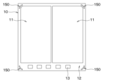
- the semiconductor device of this embodiment includes a semiconductor chip 10, a first lead frame 20, a block body 30, a second lead frame 40, a control terminal section 50, and the like.
- the semiconductor device also includes a mold resin 60 that integrally seals them.
- the first lead frame 20 corresponds to the support member.
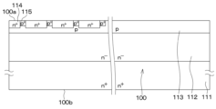
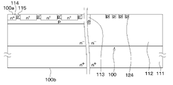
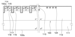
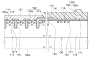
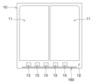
- the semiconductor chip 10 is configured to have a cell area 11 and an outer peripheral area 12 as shown in FIG.
- a MOSFET element having a gate electrode 118, a source electrode 121, a drain electrode 123 and the like is formed in the cell region 11, as shown in FIG.
- pad portions 13 connected to the gate electrode 118 and the like are formed in the peripheral region 12 .
- the first lead frame 20 is made of a highly conductive material such as copper or 42 alloy, and has a shape in which the mounting portion 21 and the main terminal portion 22 are integrally formed.
- the semiconductor chip 10 is mounted on the first lead frame 20 on the one surface 21a side of the mounting portion 21 via a bonding member 71 such as solder. Note that the mounting portion 21 and the main terminal portion 22 may be provided as separate bodies.
- the block body 30 is made of a conductive material such as copper or aluminum and has a rectangular parallelepiped shape.
- the second lead frame 40 is made of a material with excellent conductivity such as copper or 42 alloy, and has a shape in which the mounting portion 41 and the main terminal portion 42 are integrally formed. It is said that The second lead frame 40 is arranged such that the one surface 41 a side of the mounting portion 41 is connected to the joint member 73 such as solder arranged on the block body 30 . Note that the mounting portion 41 and the main terminal portion 42 may be provided as separate bodies.
- the control terminal section 50 is arranged near the semiconductor chip 10 and electrically connected to the pad section 13 formed on the semiconductor chip 10 via the wire 80 .
- the mold resin 60 is configured using a resin material such as epoxy resin.
- the molding resin 60 is formed so that the other surface 21b of the mounting portion 21 of the first lead frame 20 opposite to the surface 21a and the other surface 41b of the mounting portion 41 of the second lead frame 40 opposite to the surface 41a are exposed. are placed in Further, the mold resin 60 is arranged so that a part of each of the main terminal portions 22 and 42 and each of the control terminal portions 50 is exposed.
- the semiconductor device of this embodiment is a semiconductor device having a so-called double-sided heat dissipation structure.
- the mold resin 60 may be configured by mixing an additive (not shown) such as silica.
- FIG. 3 is a cross-sectional view along line III-III in FIG. 2, the bonding member 72 and the mold resin 60 are partially shown in order to facilitate understanding of the positional relationship. .
- the joining member 72 and the mold resin 60 are partially shown in order to facilitate understanding of the positional relationship.
- the semiconductor chip 10 has a planar shape with corners, and has a rectangular plate shape in this embodiment.
- a MOSFET element having a trench gate structure is formed as a semiconductor element.
- the outer peripheral region 12 of this embodiment is configured to have a guard ring region 12a and a connecting region 12b arranged inside the guard ring region 12a.
- the outer peripheral region 12 has a guard ring region 12a and a connecting region 12b arranged between the cell region 11 and the guard ring region 12a.
- the semiconductor chip 10 is configured using a silicon carbide (hereinafter also referred to as SiC) substrate as the semiconductor substrate 100 in this embodiment.
- the semiconductor substrate 100 may be configured using a silicon substrate or a gallium nitride substrate instead of the SiC substrate.
- the semiconductor substrate 100 of this embodiment has an n + -type substrate 111 forming a high-concentration impurity layer made of SiC.
- This substrate 111 constitutes the drain region of the MOSFET element.
- An n ⁇ -type drift layer 112 made of SiC with an impurity concentration lower than that of the substrate 111 is epitaxially grown on the substrate 111 .
- a p-type base region 113 is epitaxially grown on the drift layer 112 .
- the base region 113 is formed from the cell region 11 to the outer peripheral region 12 .
- An n + -type source region 114 is formed in the surface layer of the base region 113 of the cell region 11 .
- the surface on the side of the base region 113 is assumed to be one surface 100a of the semiconductor substrate 100, and the surface on the side of the substrate 111 is assumed to be the other surface 100b of the semiconductor substrate 100.
- the substrate 111 has, for example, an n-type impurity concentration of 1.0 ⁇ 10 19 /cm 3 and a (0001) Si surface.
- the drift layer 112 has an impurity concentration lower than that of the substrate 111.
- the n-type impurity concentration is 0.5 to 2.0 ⁇ 10 16 /cm 3 .
- the base region 113 is a portion in which a channel region is formed, and has, for example, a p-type impurity concentration of about 2.0 ⁇ 10 17 /cm 3 and a thickness of 300 nm.
- the source region 114 has a higher impurity concentration than the drift layer 112.
- the surface layer portion has an n-type impurity concentration of 2.5 ⁇ 10 18 to 1.0 ⁇ 10 19 /cm 3 and a thickness of about 0.5 ⁇ m.
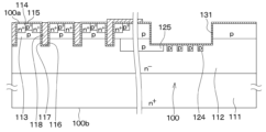
- a contact region 115 composed of a p-type high-concentration layer is formed on the surface layer of the base region 113. As shown in FIG. Specifically, the contact region 115 is formed on the opposite side of the trench 116 to be described later with the source region 114 interposed therebetween.
- a 0.8 ⁇ m wide and 1.0 ⁇ m deep conductive layer is formed so as to reach the drift layer 112 through the base region 113 and the source region 114 from the one surface 100 a side of the semiconductor substrate 100 .
- a trench 116 is formed.
- base region 113 and source region 114 are arranged to contact the side surfaces of trench 116 .
- a plurality of trenches 116 are formed in parallel at equal intervals, with the width direction in FIG.
- the trench 116 of the present embodiment extends in a direction intersecting, more specifically, a direction perpendicular to the stacking direction of the drift layer 112 and the base region 113 (hereinafter also simply referred to as the stacking direction).
- the plurality of trenches 116 extend along one direction in the planar direction of the substrate 111 .
- the trench 116 has an annular structure by being routed at the leading end in the extending direction.
- the trenches 116 may have a stripe shape in which a plurality of trenches are formed in parallel at regular intervals.
- the trench 116 is filled with the gate insulating film 117 and the gate electrode 118 .
- the trench including the channel region A gate insulating film 117 is formed on the inner wall surface of 116 .
- the gate insulating film 117 is composed of, for example, a thermal oxide film.
- a gate electrode 118 made of doped polysilicon is formed on the surface of the gate insulating film 117 .
- the gate insulating film 117 is also formed on surfaces other than the inner wall surface of the trench 116 . Specifically, the gate insulating film 117 is formed so as to also partially cover the one surface 100 a of the semiconductor substrate 100 . More specifically, gate insulating film 117 is formed to cover part of the surface of source region 114 as well. A contact hole 117a is formed in the gate insulating film 117 to expose the remaining portions of the contact region 115 and the source region 114 in a portion different from the portion where the gate electrode 118 is arranged.
- the gate insulating film 117 is also formed on the surface of the base region 113 in the outer peripheral region 12 and the like, and is also formed on the surface of the recess 131 described later.
- the gate electrode 118 extends up to the surface of the gate insulating film 117 in the connecting region 12 b of the outer peripheral region 12 .
- the trench gate structure of the present embodiment is constructed as described above.
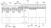
- An interlayer insulating film 119 is formed on one surface 100a of the semiconductor substrate 100 so as to cover the gate electrode 118, the gate insulating film 117, and the like.
- the interlayer insulating film 119 is made of BPSG (abbreviation of Borophosphosilicate Glass) or the like.
- a contact hole 119 a is formed in the interlayer insulating film 119 to communicate with the contact hole 117 a and expose the source region 114 and the contact region 115 .
- a contact hole is also formed in the interlayer insulating film 119 to expose a portion of the gate electrode 118 extending to the connecting region 12b.
- the contact hole 119a formed in the interlayer insulating film 119 is formed so as to communicate with the contact hole 117a formed in the gate insulating film 117, and functions as one contact hole together with the contact hole 117a. Therefore, hereinafter, the contact hole 117a and the contact hole 119a are collectively referred to as the contact hole 120 as well.
- the pattern of the contact holes 120 is arbitrary, and for example, a pattern in which a plurality of squares are arranged, a pattern in which rectangular linear holes are arranged, a pattern in which linear holes are arranged, or the like is adopted. be done. In this embodiment, the contact hole 120 is linear along the longitudinal direction of the trench 116 .
- a source electrode 121 electrically connected to the source region 114 and the contact region 115 through the contact hole 120 is formed on the interlayer insulating film 119 . Further, on the interlayer insulating film 119, a gate wiring electrically connected to the gate electrode 118 through a contact hole exposing the gate electrode 118 is formed in a cross section different from that of FIG. This gate wiring is routed as appropriate and electrically connected to one of the pad portions 13 shown in FIG.
- the source electrode 121 is formed over the entire cell region 11 and has an area sufficiently larger than that of the pad portion 13 .
- the source electrode 121 and gate wiring are composed of, for example, an Al--Si layer.
- the material forming the source electrode 121 and the gate wiring is not limited to this, and may be made of only Al or another material containing Al as a main component.
- the source electrode 121 is formed up to the boundary between the cell region 11 and the peripheral region 12 in this embodiment.
- a plated layer 122 is formed on the source electrode 121 to improve solder wettability when connecting to the outside.
- the plated layer 122 is formed by sequentially stacking a nickel plated layer and a gold plated layer from the source electrode 121 side.
- a drain electrode 123 that is electrically connected to the substrate 111 and corresponds to a second electrode is formed on the back surface of the substrate 111 (that is, the other surface 100b of the semiconductor substrate 100). With such a structure, a MOSFET device having an n-channel type inverted trench gate structure is formed.
- the semiconductor chip 10 also has a current sensor, a temperature sensor, etc. formed as appropriate. Each of these senses is appropriately electrically connected to each pad portion 13 shown in FIG.
- a recessed portion 131 reaching the drift layer 112 from the one surface 100a side of the semiconductor substrate 100 is formed.
- the recessed portion 131 is formed from the connecting region 12b to the guard ring region 12a and has the same depth as the trench 116.
- the recessed portion 131 of the present embodiment is partially recessed so as to have opposing side surfaces.
- the recess 131 of this embodiment is formed inside the outer peripheral region 12 and is not formed to reach the outer edge of the semiconductor chip 10 .
- a plurality of p-type guard rings 124 are provided on the surface layer of the drift layer 112 located below the recess 131 so as to surround the cell region 11 .
- the top layout of the guard ring 124 is, when viewed from the stacking direction, a rectangular shape with rounded corners, a circular shape, or the like.
- guard ring 124 of this embodiment is formed by, for example, ion implantation as described later. Viewing from the stacking direction means viewing from the direction normal to the plane direction of the substrate 111 .
- the guard ring region 12a may be provided with an EQR (abbreviation of Equi Potential Ring) structure or the like outside the guard ring 124 as necessary.
- a p-type RESURF layer 125 is formed on the surface layer of the drift layer 112 in the connecting region 12b.
- the RESURF layer 125 extends so as to surround the cell region 11 and reach the guard ring region 12a when viewed in the stacking direction.
- the equipotential lines can be guided toward the guard ring region 12a, and the occurrence of electric field concentration in the connecting region 12b can be suppressed. Therefore, it is possible to suppress a decrease in breakdown voltage.
- the gate insulating film 117 and the interlayer insulating film 119 are formed up to the outer peripheral region 12 , and in the portion of the outer peripheral region 12 where the recessed portion 131 is formed, it is formed along the wall surface of the recessed portion 131 . formed by However, the gate insulating film 117 and the interlayer insulating film 119 are formed so as not to fill the recess 131 .
- a protective film 140 is formed on the one surface 100a side of the semiconductor substrate 100 so as to expose the plated layer 122 .
- the protective film 140 is formed in the connecting region 12b and the guard ring region 12a.
- the protective film 140 is made of polyimide, nitride film, or the like.
- the surface roughness Ra of the surface 141 is set to 5 nm or more so as to improve adhesion to the mold resin 60. It is That is, as shown in FIG. 4, the adhesion strength of the protective film 140 to the mold resin 60 increases as the surface roughness Ra increases within a range where the surface roughness Ra is less than 5 nm. However, when the surface roughness Ra of the protective film 140 is 5 nm or more, the adhesion strength of the protective film 140 to the mold resin 60 hardly changes. Therefore, the protective film 140 has a surface roughness Ra of 5 nm or more.
- the protective film 140 is made of polyimide, similar results are obtained when the protective film 140 is made of a nitride film or the like. Further, the surface roughness Ra of the protective film 140 is adjusted by performing blasting or the like, for example.
- An uneven structure 150 is formed on the surface 141 of the protective film 140 opposite to the semiconductor substrate 100 .
- the concave-convex structure 150 is formed in the protective film 140 by forming a concave portion 140 a corresponding to the concave portion 131 in a portion positioned above the concave portion 131 .
- the concave-convex structure 150 of the present embodiment is formed in a frame shape along the outer edge of the semiconductor chip 10 so as to surround the cell region 11 and the pad section 13 . Mold resin 60 is arranged so as to enter recess 140a.
- the recessed portion 140a of the present embodiment is formed by forming the protective film 140 on the recessed portion 131. As shown in FIG. Therefore, recessed portion 131 and gate insulating film 117 and interlayer insulating film 119 formed on recessed portion 131 are formed so as to suppress disappearance of recessed portion 140a when protective film 140 is formed. For example, if the distance between the interlayer insulating films 119 formed on the opposing side surfaces of the recess 131 is d, and the thickness of the protective film 140 is t, the size of the recess 131 should be such that d ⁇ 2t. Preferably, the thicknesses of gate insulating film 117 and interlayer insulating film 119 are adjusted. Further, the recess 140a has a depth of, for example, about 1 ⁇ m.
- the semiconductor chip 10 since the semiconductor chip 10 is configured as described above, when the mold resin 60 is peeled off from the semiconductor chip 10, the peeling reaches the source electrode 121 and the like located on the inner edge side. can be suppressed. That is, when the mold resin 60 is peeled off from the semiconductor chip 10 , this peeling is likely to occur from the outer edge of the interface between the protective film 140 and the mold resin 60 . This peeling easily spreads along the interface between the protective film 140 and the mold resin 60 .
- the concave-convex structure 150 since the concave-convex structure 150 is formed, when the separation reaches the concave-convex structure 150, the extension direction of the separation changes. Therefore, the extension of peeling can be suppressed, and the peeling can be prevented from reaching the source electrode 121 or the like.
- the angle ⁇ 1 between the surface 141 and the side surface 142a of the recess 140a is preferably 45° or more. That is, when the peeling reaches the concave portion 140 a from the outer edge, the stress affecting the peeling is the stress in the direction along the stretching direction and the stress in the direction along the interface between the protective film 140 and the mold resin 60 . is distributed over the stress of Therefore, by setting the angle ⁇ 1 to be 45° or more, the stress in the direction along the interface between the protective film 140 and the mold resin 60 can be easily made larger than the stress in the direction along the extending direction of peeling. Therefore, it becomes easier to change the direction of propagation of half or more of the stress that affects detachment, and it is possible to further suppress detachment from reaching the source electrode 121 and the like.
- the semiconductor substrate 100 is constructed by forming the drift layer 112 and the base region 113 on the substrate 111 .
- the drift layer 112 and the base region 113 are formed by epitaxial growth or the like on the surface side of the substrate 111, for example.
- a source region 114 and a contact region 115 are formed in order by placing a mask (not shown) on the one surface 100a side of the semiconductor substrate 100 and performing ion implantation or the like.
- a mask (not shown) is placed on the one surface 100a side of the semiconductor substrate 100 and anisotropic etching or the like is performed to form trenches 116 and recesses 131 .
- the trench 116 and the depression 131 are formed in the same process, the trench 116 and the depression 131 have the same depth.
- the trench 116 and the recessed portion 131 may be formed in separate processes so that the trenches 116 and the recessed portion 131 have different depths.
- a gate insulating film 117 is formed on the wall surface of the trench 116, the one surface 100a of the semiconductor substrate 100, and the wall surface of the recess 131 by thermal oxidation or the like. Then, a CVD (abbreviation of chemical vapor deposition) method, patterning, or the like is performed to form the gate electrode 118 . Note that the gate electrode 118 extends to the connecting region 12b as described above.
- a guard ring 124 and a RESURF layer 125 are formed by placing a mask (not shown) on the one surface 100a side of the semiconductor substrate 100 and performing ion implantation or the like.
- an interlayer insulating film 119 is formed by the CVD method or the like.
- a contact hole 120 is formed by placing a mask (not shown) on the interlayer insulating film 119 and performing anisotropic etching or the like.
- the source electrode 121 is formed by the CVD method, patterning, or the like.
- a protective film 140 is formed by CVD, patterning, or the like.
- the recessed portion 140a is formed on the surface 141 of the protective film 140 due to the recessed portion 131, and the concave-convex structure 150 is formed by the recessed portion 140a.
- the concave portion 140a is formed so that the angle ⁇ 1 formed by the surface 141 and the side surface 142a is 45° or more as described above.
- the conditions for forming the protective film 140, the shape of the recess 140a, the thicknesses of the gate insulating film 117 and the interlayer insulating film 119, etc. may be adjusted so that the formed angle ⁇ 1 is 45° or more. preferable.
- the semiconductor chip 10 is manufactured by forming the drain electrode 123 and the like on the other surface 100b side of the semiconductor substrate 100 .
- the surface 141 of the protective film 140 has a surface roughness of 5 nm or more. For this reason, it is possible to suppress a decrease in adhesion strength between the protective film 140 and the mold resin 60 , and it is possible to suppress peeling of the mold resin 60 from the semiconductor chip 10 .
- the protective film 140 has an uneven structure 150 formed on the surface 141 thereof. Therefore, when the mold resin 60 is peeled off from the outer edge of the protective film 140 of the semiconductor chip 10, the extension direction of the peeling can be changed by the uneven structure 150, and the stress for extending the peeling can be reduced. Therefore, it is possible to prevent the peeling from extending to the inner edge of the semiconductor chip 10 . Since the peeling is prevented from reaching the inner edge of the semiconductor chip 10 in this way, a SiC substrate or the like having a high Young's modulus can be used as the semiconductor substrate 100, and the selectivity of the semiconductor substrate 100 can be improved. can be planned.
- the concave portion 140 a is formed on the surface of the protective film 140 by forming the concave portion 131 of the semiconductor substrate 100 . Therefore, the recesses 140a can be formed on the surface 141 of the protective film 140 by an easy method.
- the mold resin 60 when the mold resin 60 is peeled off from the semiconductor chip 10 , the mold resin 60 is easily peeled off from the outer edge of the semiconductor chip 10 . Therefore, by forming the uneven structure 150 so as to surround the cell region 11 and the pad section 13 as in the present embodiment, the uneven structure 150 is formed between the starting point of peeling and the source electrode 121 and the pad section 13 . formed in Therefore, the uneven structure 150 can effectively prevent the peeling from reaching the source electrode 121 and the pad portion 13 .
- the concave portion 140a has an angle ⁇ 1 formed by the surface 141 and the side surface 142a of 45° or more. This makes it easier to increase the stress in the direction along the interface between the protective film 140 and the mold resin 60 than the stress in the direction along the extension direction of the peeling (that is, the surface direction of the semiconductor substrate 100). Therefore, it is possible to further prevent the delamination from reaching the inner edge side of the semiconductor chip 10 .
- the recess 131 and the RESURF layer 125 are not formed in the semiconductor substrate 100 .
- the guard ring 124 is formed from the one surface 100 a side of the semiconductor substrate 100 .
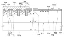
- a stopper wiring 160 is formed on the gate insulating film 117 formed on the one surface 100 a of the semiconductor substrate 100 on the outer edge side of the guard ring 124 .
- the stopper wiring 160 of this embodiment is not electrically connected to other electrodes or the like, and is at a floating potential.
- the stopper wiring 160 of this embodiment is composed of a dummy wiring.
- the stopper wiring 160 of the present embodiment is configured using the same material as the gate electrode 118 . In this embodiment, the stopper wiring 160 corresponds to the stopper member.
- the interlayer insulating film 119 has an opening 119b that exposes a portion of the stopper wiring 160 in a portion that covers the stopper wiring 160 .
- the opening 119b of this embodiment is formed at the same time as the contact hole 120, as will be described later.
- the protective film 140 is arranged on the interlayer insulating film 119 as described above.
- the protective film 140 is arranged so as to fill the opening 119b of the interlayer insulating film 119, and a recess 140a depending on the opening 119b is formed on the surface 141 side.
- the concave-convex structure 150 can be arranged so as to include a portion where the guard ring 124 is not arranged due to the rounding in the stacking direction. preferable. As a result, it is possible to prevent the semiconductor chip 10 from increasing in size.
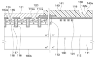
- a semiconductor substrate 100 having a drift layer 112 is prepared. Then, as shown in FIG. 7B, a base region 113, a source region 114, a contact region 115, and a guard ring 124 are formed in order by placing a mask (not shown) and performing ion implantation or the like.
- trenches 116 are formed by performing the same process as the process of FIG. 5C. However, in this embodiment, the recessed portion 131 is not formed.
- the gate insulating film 117 and the gate electrode 118 are formed in order by performing the same process as the process of FIG. 5D.
- the stopper wiring 160 is formed at the same time as the gate electrode 118 is formed by patterning. Therefore, the stopper wiring 160 of this embodiment is made of the same material as the gate electrode 118 .
- the opening 119b for exposing the stopper wiring 160 is also formed at the same time.
- the stopper wiring 160 can prevent the semiconductor substrate 100 from being etched when the opening 119b is exposed. That is, the stopper wiring 160 of this embodiment also functions as an etching stopper.
- the source electrode 121 is formed by performing the same process as the process of FIG. 5G.
- the protective film 140 is formed by performing the same process as the process of FIG. 5H.
- a concave portion 140a is formed on the surface 141 of the protective film 140 due to the opening 119b.
- the semiconductor chip 10 is manufactured by forming the drain electrode 123 and the like on the other surface 100b side of the semiconductor substrate 100 .
- the protective film 140 has a surface roughness of 5 nm or more and the uneven structure 150 is formed on the surface 141, the same effects as those of the first embodiment can be obtained. can be done.
- the recess 140a is formed on the surface of the protective film 140 by forming the opening 119b in the interlayer insulating film 119 . Even if the concave portion 140a is formed on the surface 141 of the protective film 140 in this way, the concave portion 140a can be formed on the surface 141 of the protective film 140 by an easy method. Further, in this embodiment, the stopper wiring 160 is formed so as to be exposed from the opening 119b. Therefore, when the opening 119b is formed in the interlayer insulating film 119, etching of the semiconductor substrate 100 can be suppressed.
- the stopper wiring 160 may be configured using a material different from that of the gate electrode 118, or may be configured using an insulating material.
- the stopper wiring 160 is made of the same material as the gate electrode 118 and is formed at the same time as the gate electrode 118 is formed.
- the opening 119b of the interlayer insulating film 119 is formed at the same time as the contact hole 120 is formed. Therefore, the concave portion 140a can be formed in the surface 141 of the protective film 140 while suppressing an increase in the number of manufacturing processes.
- the uneven structure 150 is formed closer to the outer edge than the guard ring 124 . Therefore, when the mold resin 60 is peeled off from the outer edge of the semiconductor chip 10, the extension of the peeling can be suppressed at an early stage.
- the recess 140a is formed in the surface 141 of the protective film 140, but the interlayer insulating film 119 is not formed with the opening 119b. Also, the stopper wiring 160 in the second embodiment is not arranged.
- the same step as the step of FIG. 5D is performed to form the gate insulating film 117 and the gate electrode 118.
- the gate electrode 118 is formed so that the stopper wiring 160 is not formed.
- an interlayer insulating film 119 is formed and a contact hole 120 is formed in the interlayer insulating film 119 by performing the same step as the step shown in FIG. 7F.
- the source electrode 121 is formed by performing the same process as the process of FIG. 7G.
- the protective film 140 is formed by performing the same process as the process of FIG. 7H.
- the opening 119b is not formed in this embodiment, the surface 141 is substantially flattened after the process of FIG. 9D is performed.
- a recess 140a is formed in the protective film 140 by etching the protective film 140 using a photoresist (not shown) as a mask. Thereafter, although not shown, the semiconductor chip 10 is manufactured by forming the drain electrode 123 and the like on the other surface 100b side of the semiconductor substrate 100. Next, as shown in FIG. 9E, a photoresist (not shown) as a mask. Thereafter, although not shown, the semiconductor chip 10 is manufactured by forming the drain electrode 123 and the like on the other surface 100b side of the semiconductor substrate 100. Next, as shown in FIG.
- the protective film 140 has a surface roughness of 5 nm or more and the uneven structure 150 is formed on the surface 141, the same effects as those of the first embodiment can be obtained. can be done.
- the recesses 140a are formed on the surface of the protective film 140 by etching. Therefore, the shape of the concave portion 140a can be easily adjusted, and the angle ⁇ 1 formed between the surface 141 and the side surface 142a can be easily adjusted in detail.
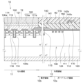
- the protrusion wiring 170 is formed on the interlayer insulating film 119 on the outer edge side of the guard ring 124 .
- the wiring 170 for a convex portion is not electrically connected to other electrodes or the like, and is at a floating potential.
- the wiring 170 for the convex portion of the present embodiment is composed of a dummy wiring.
- the wiring 170 for projections of the present embodiment is configured using the same material as the source electrode 121 . In this embodiment, the projection wiring 170 corresponds to the projection member.
- the protective film 140 is arranged on the interlayer insulating film 119 as described above, and arranged so as to also cover the wiring 170 for the convex portion. Therefore, the protective film 140 is formed with a convex portion 140 b caused by the wiring 170 for convex portion on the surface 141 side. It is preferable that the angle ⁇ 2 between the side surface 142b of the protrusion 140b and the surface 141 is 45° or more, as in the first embodiment. Further, in the present embodiment, the uneven structure 150 is configured by the protrusions 140b.
- the same step as in FIG. 9C is performed to form the source electrode 121 .
- the wiring 170 for the projection remains. For this reason, the wiring 170 for projections of the present embodiment is made of the same material as the source electrode 121 .
- a protective film 140 is formed by performing the same process as the process of FIG. 9D.
- a projection 140b is formed on the surface 141 of the protective film 140 due to the wiring 170 for projections.
- the semiconductor chip 10 is manufactured by forming the drain electrode 123 and the like on the other surface 100b side of the semiconductor substrate 100.
- the protective film 140 since the protective film 140 has a surface roughness of 5 nm or more and the uneven structure 150 is formed on the surface 141, the same effects as those of the first embodiment can be obtained. can be done.
- the stress direction of the separation is changed by the convex portion 140b.
- the protrusion 140b is formed on the surface of the protective film 140 by forming the protrusion wiring 170 on the interlayer insulating film 119 . Even if the convex portions 140b are formed on the surface of the protective film 140 in this way, the convex portions 140b can be formed on the surface 141 of the protective film 140 by a simple method.
- the projection wiring 170 is made of the same material as the source electrode 121 and is formed at the same time as the source electrode 121 is formed. Therefore, it is possible to form the protrusions 140b on the surface 141 of the protective film 140 while suppressing an increase in the number of manufacturing processes.
- the wiring 170 for the projection may not be made of the same material as the source electrode 121, and may be made of the same material as the other wirings.
- the projection wiring 170 may be made of the same material as the wiring forming the EQR structure.
- the wiring 170 for the projection (that is, the member for the projection) may be made of a material different from that of each wiring, or may be made of an insulating material.
- the convex portion 140b is formed on the surface 141 of the protective film 140, but the wiring 170 for convex portion is not formed.
- the convex portion 140 b of the present embodiment is configured by arranging the protrusion portion 180 on the surface of the protective film 140 .
- the protruding portion 180 is formed by forming the protective film 140, then applying a material in a convex shape using a dispenser, a 3D printer, or the like, and curing the material.
- the protrusion 180 may be made of the same material as the protective film 140, or may be made of a different material.
- the surface roughness of the protective film 140 is set to 5 nm or more and the uneven structure 150 is formed on the surface 141, the same effects as those of the fourth embodiment can be obtained. can be done.
- the uneven structure 150 is arranged between the corner of the semiconductor chip 10 and the cell region 11 and the pad portion 13 in the outer peripheral region 12 .
- the formation location of the concave-convex structure 150 of this embodiment can also be applied to the above-described second to fifth embodiments.
- the concave-convex structure 150 is preferably arranged so as to include a portion where the guard ring 124 is not arranged due to the rounding in the stacking direction. . As a result, it is possible to prevent the semiconductor chip 10 from increasing in size.
- the protective film 140 has a surface roughness of 5 nm or more and the uneven structure 150 is formed on the surface 141, the same effects as those of the first embodiment can be obtained. can be done.
- the mold resin 60 when the mold resin 60 is peeled off from the semiconductor chip 10 , the mold resin 60 is easily peeled off from the outer edge of the semiconductor chip 10 . It is easy to peel off from the part. Therefore, by arranging the uneven structure 150 between the corner of the semiconductor chip 10 and the cell region 11 and the pad portion 13 as in the present embodiment, the uneven structure 150 prevents the source electrode 121 and the pad portion 13 from peeling off. can be effectively suppressed from reaching
- the plane area of the source electrode 121 is sufficiently larger than that of the pad portion 13 . Therefore, when the mold resin 60 is peeled off from the semiconductor chip 10 and the peeling reaches the pad portion 13 , the effect is greater than when the peeling reaches the source electrode 121 .
- the uneven structure 150 is formed so as to surround each pad portion 13 as shown in FIG.
- the protective film 140 has a surface roughness of 5 nm or more and the uneven structure 150 is formed on the surface 141, the same effects as those of the first embodiment can be obtained. can be done.
- the uneven structure 150 is formed so as to surround the pad section 13 . Therefore, it is possible to prevent the peeling from reaching at least the pad portion 13, which is greatly affected by the peeling. In addition, since the space around the pad portion 13 is widened due to restrictions of the wire bonding apparatus, etc., by arranging the uneven structure 150 in this space, it is possible to prevent the semiconductor chip 10 from increasing in size.
- the concave-convex structure 150 is formed so as to substantially surround the pad section 13 rather than completely surrounding the pad section 13 .
- the concave-convex structure 150 is formed in a substantially U shape so as not to block the portion of the pad portion 13 on the cell region 11 side.
- the uneven structure 150 is formed so as not to cross the imaginary line connecting the pad portion 13 and the cell region 11 .
- the mold resin 60 is peeled off as described above, peeling is likely to occur from the corners of the semiconductor chip 10 . It is preferably formed in
- the protective film 140 has a surface roughness of 5 nm or more and the uneven structure 150 is formed on the surface 141, the same effects as those of the first embodiment can be obtained. can be done.
- the uneven structure 150 can prevent the peeling from reaching the pad portion 13. You can get the same effect as the form.
- the connection wiring can be easily arranged through the unsurrounded portion, and the degree of freedom in design can be improved.
- the uneven structure 150 is arranged between the pad section 13 and the outer edge of the semiconductor chip 10 .
- the protective film 140 has a surface roughness of 5 nm or more and the uneven structure 150 is formed on the surface 141, the same effects as those of the first embodiment can be obtained. can be done.
- the uneven structure 150 prevents the peeling from reaching the pad portion 13 . Since it can be suppressed, the same effect as the eighth embodiment can be obtained.
- the semiconductor elements formed on the semiconductor chip 10 can be changed as appropriate.
- the semiconductor element may be a p-channel type trench gate structure MOSFET in which the conductivity type of each component is inverted with respect to the n-channel type.
- the semiconductor element may be configured to have an IGBT having a similar structure other than the MOSFET.
- the IGBT is the same as the MOSFET described in the first embodiment except that the n + -type substrate 111 in the first embodiment is changed to a p + -type collector layer.
- the gate structure may be a planar gate structure instead of a trench gate structure.
- the uneven structure 150 may be formed so as to reach the outer edge of the semiconductor chip 10 in a non-restricted portion on the semiconductor chip 10 .
- the recess 140a formed on the surface 141 of the protective film 140 is formed to reach the outer edge of the semiconductor chip 10 and does not have side surfaces facing each other. good.
- the semiconductor device includes the first lead frame 20 and the second lead frame 40, and the other surface 21b of the first lead frame 20 and the other surface 41b of the second lead frame 40 are exposed from the mold resin 60.
- the configuration of the semiconductor device is not limited to this.
- the semiconductor device may have a single-sided heat dissipation structure in which heat is dissipated only from the drain electrode 123 side of the semiconductor chip 10 .
- a single-sided heat dissipation structure as shown in FIG. may be connected to Further, as shown in FIG.
- a lead terminal portion 92 may be arranged on the source electrode 121 with a bonding member 72 interposed therebetween so that a portion of the lead terminal portion 92 is exposed from the mold resin 60 .
- the semiconductor device may be configured such that the mold resin 60 is arranged to cover the other surface 21 b of the first lead frame 20 and the other surface 41 b of the second lead frame 40 .
- the uneven structure 150 may be formed closer to the outer edge than the guard ring 124 when viewed from the stacking direction.
- the concave-convex structure 150 may be formed on the guard ring 124 as in the first embodiment.
- the protective film 140 may include at least one of the concave portions 140a of the first to third embodiments and at least one of the convex portions 140b of the fourth and fifth embodiments. That is, the concave-convex structure 150 formed on the protective film 140 may include a plurality of different concave portions 140a and convex portions 140b.
- the formation locations of the concave-convex structures 150 in the sixth to ninth embodiments can be appropriately applied to the first to fifth embodiments.
Landscapes
- Electrodes Of Semiconductors (AREA)
- Structures Or Materials For Encapsulating Or Coating Semiconductor Devices Or Solid State Devices (AREA)
- Insulated Gate Type Field-Effect Transistor (AREA)
Priority Applications (2)
| Application Number | Priority Date | Filing Date | Title |
|---|---|---|---|
| CN202280059482.0A CN117916892A (zh) | 2021-09-03 | 2022-08-31 | 半导体装置 |
| US18/420,125 US20240203811A1 (en) | 2021-09-03 | 2024-01-23 | Semiconductor device |
Applications Claiming Priority (2)
| Application Number | Priority Date | Filing Date | Title |
|---|---|---|---|
| JP2021143928A JP7586034B2 (ja) | 2021-09-03 | 2021-09-03 | 半導体装置 |
| JP2021-143928 | 2021-09-03 |
Related Child Applications (1)
| Application Number | Title | Priority Date | Filing Date |
|---|---|---|---|
| US18/420,125 Continuation US20240203811A1 (en) | 2021-09-03 | 2024-01-23 | Semiconductor device |
Publications (1)
| Publication Number | Publication Date |
|---|---|
| WO2023033047A1 true WO2023033047A1 (ja) | 2023-03-09 |
Family
ID=85411278
Family Applications (1)
| Application Number | Title | Priority Date | Filing Date |
|---|---|---|---|
| PCT/JP2022/032778 Ceased WO2023033047A1 (ja) | 2021-09-03 | 2022-08-31 | 半導体装置 |
Country Status (4)
| Country | Link |
|---|---|
| US (1) | US20240203811A1 (https=) |
| JP (2) | JP7586034B2 (https=) |
| CN (1) | CN117916892A (https=) |
| WO (1) | WO2023033047A1 (https=) |
Cited By (1)
| Publication number | Priority date | Publication date | Assignee | Title |
|---|---|---|---|---|
| WO2025225054A1 (ja) * | 2024-04-23 | 2025-10-30 | 三菱電機株式会社 | 半導体装置、電力変換装置、及び、半導体装置の製造方法 |
Families Citing this family (2)
| Publication number | Priority date | Publication date | Assignee | Title |
|---|---|---|---|---|
| JP7717010B2 (ja) * | 2022-03-08 | 2025-08-01 | 株式会社デンソー | 半導体装置 |
| JP2024157928A (ja) * | 2023-04-26 | 2024-11-08 | 株式会社デンソー | 半導体装置およびその製造方法 |
Citations (6)
| Publication number | Priority date | Publication date | Assignee | Title |
|---|---|---|---|---|
| JP2005317860A (ja) * | 2004-04-30 | 2005-11-10 | Fujitsu Ltd | 樹脂封止型半導体装置 |
| JP2007158113A (ja) * | 2005-12-06 | 2007-06-21 | Toyota Motor Corp | 半導体装置とその製造方法 |
| JP2017092212A (ja) * | 2015-11-09 | 2017-05-25 | 株式会社東芝 | 半導体装置およびその製造方法 |
| JP2018029162A (ja) * | 2016-08-19 | 2018-02-22 | 信越半導体株式会社 | 発光素子及び発光素子の製造方法 |
| WO2020012810A1 (ja) * | 2018-07-11 | 2020-01-16 | 住友電気工業株式会社 | 炭化珪素半導体装置 |
| JP6887541B1 (ja) * | 2020-02-21 | 2021-06-16 | 三菱電機株式会社 | 半導体装置 |
Family Cites Families (15)
| Publication number | Priority date | Publication date | Assignee | Title |
|---|---|---|---|---|
| JPH06140563A (ja) * | 1992-10-23 | 1994-05-20 | Rohm Co Ltd | 半導体装置 |
| JP3561821B2 (ja) * | 1995-12-01 | 2004-09-02 | 日本テキサス・インスツルメンツ株式会社 | 半導体パッケージ装置 |
| JP2005150419A (ja) * | 2003-11-17 | 2005-06-09 | Nippon Soken Inc | 半導体装置 |
| US7687326B2 (en) * | 2004-12-17 | 2010-03-30 | Semiconductor Energy Laboratory Co., Ltd. | Semiconductor device and manufacturing method thereof |
| JP2006196710A (ja) | 2005-01-13 | 2006-07-27 | Fuji Electric Device Technology Co Ltd | 半導体素子の製造方法 |
| JP4535151B2 (ja) | 2008-03-19 | 2010-09-01 | 株式会社デンソー | 炭化珪素半導体装置の製造方法 |
| JP5729126B2 (ja) * | 2011-05-18 | 2015-06-03 | 株式会社デンソー | 半導体装置の製造方法 |
| JP5970316B2 (ja) * | 2012-09-26 | 2016-08-17 | ルネサスエレクトロニクス株式会社 | 半導体装置の製造方法 |
| JP6102354B2 (ja) * | 2013-03-06 | 2017-03-29 | トヨタ自動車株式会社 | 逆導通igbt |
| US9947553B2 (en) * | 2015-01-16 | 2018-04-17 | Rohm Co., Ltd. | Manufacturing method of semiconductor device and semiconductor device |
| JP6274154B2 (ja) * | 2015-05-27 | 2018-02-07 | トヨタ自動車株式会社 | 逆導通igbt |
| US10593788B2 (en) * | 2016-07-11 | 2020-03-17 | Pui Sze LAU | Reverse-conducting insulated-gate bipolar transistor structure and corresponding fabrication method thereof |
| JP2018022776A (ja) * | 2016-08-03 | 2018-02-08 | ルネサスエレクトロニクス株式会社 | 半導体装置 |
| JP7099546B2 (ja) * | 2018-12-19 | 2022-07-12 | 富士電機株式会社 | 半導体装置 |
| JP7180490B2 (ja) * | 2019-03-26 | 2022-11-30 | 株式会社デンソー | 半導体装置およびその製造方法 |
-
2021
- 2021-09-03 JP JP2021143928A patent/JP7586034B2/ja active Active
-
2022
- 2022-08-31 WO PCT/JP2022/032778 patent/WO2023033047A1/ja not_active Ceased
- 2022-08-31 CN CN202280059482.0A patent/CN117916892A/zh active Pending
-
2024
- 2024-01-23 US US18/420,125 patent/US20240203811A1/en active Pending
- 2024-10-31 JP JP2024191937A patent/JP7806870B2/ja active Active
Patent Citations (6)
| Publication number | Priority date | Publication date | Assignee | Title |
|---|---|---|---|---|
| JP2005317860A (ja) * | 2004-04-30 | 2005-11-10 | Fujitsu Ltd | 樹脂封止型半導体装置 |
| JP2007158113A (ja) * | 2005-12-06 | 2007-06-21 | Toyota Motor Corp | 半導体装置とその製造方法 |
| JP2017092212A (ja) * | 2015-11-09 | 2017-05-25 | 株式会社東芝 | 半導体装置およびその製造方法 |
| JP2018029162A (ja) * | 2016-08-19 | 2018-02-22 | 信越半導体株式会社 | 発光素子及び発光素子の製造方法 |
| WO2020012810A1 (ja) * | 2018-07-11 | 2020-01-16 | 住友電気工業株式会社 | 炭化珪素半導体装置 |
| JP6887541B1 (ja) * | 2020-02-21 | 2021-06-16 | 三菱電機株式会社 | 半導体装置 |
Cited By (1)
| Publication number | Priority date | Publication date | Assignee | Title |
|---|---|---|---|---|
| WO2025225054A1 (ja) * | 2024-04-23 | 2025-10-30 | 三菱電機株式会社 | 半導体装置、電力変換装置、及び、半導体装置の製造方法 |
Also Published As
| Publication number | Publication date |
|---|---|
| JP2023037280A (ja) | 2023-03-15 |
| JP7586034B2 (ja) | 2024-11-19 |
| JP7806870B2 (ja) | 2026-01-27 |
| US20240203811A1 (en) | 2024-06-20 |
| CN117916892A (zh) | 2024-04-19 |
| JP2025016654A (ja) | 2025-02-04 |
Similar Documents
| Publication | Publication Date | Title |
|---|---|---|
| JP7806870B2 (ja) | 半導体装置 | |
| JP6143490B2 (ja) | 半導体装置およびその製造方法 | |
| US20210234007A1 (en) | SiC SEMICONDUCTOR DEVICE | |
| CN116314289A (zh) | 半导体装置 | |
| CN108550618A (zh) | 半导体装置 | |
| US12100763B2 (en) | Semiconductor device having cell section with gate structures partly covered with protective film | |
| JP7319072B2 (ja) | 半導体装置 | |
| CN113410288B (zh) | 半导体装置 | |
| CN115868013A (zh) | 半导体装置 | |
| JP7001050B2 (ja) | 半導体装置 | |
| US11410946B2 (en) | Semiconductor apparatus | |
| JP7388433B2 (ja) | 半導体装置 | |
| JP2023082869A (ja) | 半導体装置 | |
| US20240096990A1 (en) | Semiconductor device and method of manufacturing semiconductor device | |
| US20250029883A1 (en) | Semiconductor module and method for manufacturing semiconductor module | |
| US20250318222A1 (en) | Semiconductor device and method of manufacturing the same | |
| JP2023175143A (ja) | 半導体装置 | |
| JP2006216596A (ja) | 半導体装置およびその製造方法 | |
| JP2023177564A (ja) | 半導体装置 | |
| JP2023010376A (ja) | 半導体装置 | |
| JP2022010220A (ja) | 半導体装置 | |
| US20240006475A1 (en) | Semiconductor device and semiconductor module | |
| JP2026056452A (ja) | 半導体装置及びその製造方法 | |
| WO2023090137A1 (ja) | 半導体素子および半導体装置 | |
| JP2025138292A (ja) | 半導体装置 |
Legal Events
| Date | Code | Title | Description |
|---|---|---|---|
| 121 | Ep: the epo has been informed by wipo that ep was designated in this application |
Ref document number: 22864629 Country of ref document: EP Kind code of ref document: A1 |
|
| WWE | Wipo information: entry into national phase |
Ref document number: 202280059482.0 Country of ref document: CN |
|
| NENP | Non-entry into the national phase |
Ref country code: DE |
|
| 122 | Ep: pct application non-entry in european phase |
Ref document number: 22864629 Country of ref document: EP Kind code of ref document: A1 |