WO2023021952A1 - 処理方法及び処理システム - Google Patents
処理方法及び処理システム Download PDFInfo
- Publication number
- WO2023021952A1 WO2023021952A1 PCT/JP2022/029027 JP2022029027W WO2023021952A1 WO 2023021952 A1 WO2023021952 A1 WO 2023021952A1 JP 2022029027 W JP2022029027 W JP 2022029027W WO 2023021952 A1 WO2023021952 A1 WO 2023021952A1
- Authority
- WO
- WIPO (PCT)
- Prior art keywords
- substrate
- laser
- wafer
- region
- interface
- Prior art date
- Legal status (The legal status is an assumption and is not a legal conclusion. Google has not performed a legal analysis and makes no representation as to the accuracy of the status listed.)
- Ceased
Links
Images


Classifications
-
- H—ELECTRICITY
- H10—SEMICONDUCTOR DEVICES; ELECTRIC SOLID-STATE DEVICES NOT OTHERWISE PROVIDED FOR
- H10P—GENERIC PROCESSES OR APPARATUS FOR THE MANUFACTURE OR TREATMENT OF DEVICES COVERED BY CLASS H10
- H10P52/00—Grinding, lapping or polishing of wafers, substrates or parts of devices
-
- H—ELECTRICITY
- H10—SEMICONDUCTOR DEVICES; ELECTRIC SOLID-STATE DEVICES NOT OTHERWISE PROVIDED FOR
- H10P—GENERIC PROCESSES OR APPARATUS FOR THE MANUFACTURE OR TREATMENT OF DEVICES COVERED BY CLASS H10
- H10P72/00—Handling or holding of wafers, substrates or devices during manufacture or treatment thereof
- H10P72/04—Apparatus for manufacture or treatment
- H10P72/0402—Apparatus for fluid treatment
- H10P72/0406—Apparatus for fluid treatment for cleaning followed by drying, rinsing, stripping, blasting or the like
-
- H—ELECTRICITY
- H10—SEMICONDUCTOR DEVICES; ELECTRIC SOLID-STATE DEVICES NOT OTHERWISE PROVIDED FOR
- H10P—GENERIC PROCESSES OR APPARATUS FOR THE MANUFACTURE OR TREATMENT OF DEVICES COVERED BY CLASS H10
- H10P72/00—Handling or holding of wafers, substrates or devices during manufacture or treatment thereof
- H10P72/30—Handling or holding of wafers, substrates or devices during manufacture or treatment thereof for conveying, e.g. between different workstations
- H10P72/32—Handling or holding of wafers, substrates or devices during manufacture or treatment thereof for conveying, e.g. between different workstations between different workstations
- H10P72/3218—Conveying cassettes, containers or carriers
-
- H—ELECTRICITY
- H10—SEMICONDUCTOR DEVICES; ELECTRIC SOLID-STATE DEVICES NOT OTHERWISE PROVIDED FOR
- H10P—GENERIC PROCESSES OR APPARATUS FOR THE MANUFACTURE OR TREATMENT OF DEVICES COVERED BY CLASS H10
- H10P72/00—Handling or holding of wafers, substrates or devices during manufacture or treatment thereof
- H10P72/70—Handling or holding of wafers, substrates or devices during manufacture or treatment thereof for supporting or gripping
- H10P72/76—Handling or holding of wafers, substrates or devices during manufacture or treatment thereof for supporting or gripping using mechanical means, e.g. clamps or pinches
- H10P72/7604—Handling or holding of wafers, substrates or devices during manufacture or treatment thereof for supporting or gripping using mechanical means, e.g. clamps or pinches the wafers being placed on a susceptor, stage or support
- H10P72/7618—Handling or holding of wafers, substrates or devices during manufacture or treatment thereof for supporting or gripping using mechanical means, e.g. clamps or pinches the wafers being placed on a susceptor, stage or support characterised by a movable susceptor, stage or support, others than those only rotating on their own vertical axis, e.g. susceptors on a rotating carrousel
-
- H—ELECTRICITY
- H10—SEMICONDUCTOR DEVICES; ELECTRIC SOLID-STATE DEVICES NOT OTHERWISE PROVIDED FOR
- H10P—GENERIC PROCESSES OR APPARATUS FOR THE MANUFACTURE OR TREATMENT OF DEVICES COVERED BY CLASS H10
- H10P95/00—Generic processes or apparatus for manufacture or treatments not covered by the other groups of this subclass
Definitions
- the present disclosure relates to processing methods and processing systems.
- Patent Document 1 in a superimposed substrate in which a first substrate and a second substrate are bonded, a reforming agent is introduced into the inside of the first substrate along the boundary between the peripheral edge portion and the central portion of the first substrate to be removed.
- a substrate processing system includes a modified layer forming device for forming a layer and a peripheral edge removing device for removing a peripheral edge portion of a first substrate with the modified layer as a starting point.
- the technique according to the present disclosure appropriately removes part or all of the first substrate in the superposed substrate in which the first substrate and the second substrate are bonded.
- One aspect of the present disclosure is a method of processing a polymerized substrate in which a first substrate and a second substrate are bonded, comprising obtaining layer information of the polymerized substrate; irradiating a laser absorption film formed on the interface of the substrate with a pulsed laser beam to form an unbonded region in which bonding strength between the first substrate and the second substrate is reduced; separating the first substrate from the second substrate; and forming the unbonded region, a region directly under irradiation of the laser light including one focal point of the laser light irradiated in a pulsed manner.
- the present disclosure it is possible to appropriately remove part or all of the first substrate in the polymerized substrate in which the first substrate and the second substrate are bonded.
- FIG. 1 is a plan view showing an outline of the configuration of a wafer processing system according to this embodiment;
- FIG. It is a side view which shows the outline of a structure of an interfacial modification apparatus.
- FIG. 3 is an explanatory diagram showing main steps of wafer processing in the wafer processing system;
- FIG. 10 is a cross-sectional view showing the appearance of the superposed wafer after forming the unbonded region;
- FIG. 4 is an explanatory diagram showing a temperature distribution during irradiation of interface laser light; 4 is a table showing delamination states of the first wafer under various conditions;
- FIG. 10 is an explanatory diagram showing another irradiation example of interface laser light;
- FIG. 10 is an explanatory diagram showing another irradiation example of interface laser light;
- FIG. 4 is a side view showing another configuration of the interfacial modification device;
- FIG. 5 is an explanatory diagram showing another configuration of the cooling mechanism;
- FIG. 5 is an explanatory diagram showing another configuration of the cooling mechanism;
- FIG. 10 is an explanatory diagram showing another application example of the technology according to the present disclosure;
- FIG. 4 is an explanatory diagram of a laser shape of an interface laser beam;
- FIG. 10 is an explanatory diagram of a modification example of the laser shape of the interface laser light;
- FIG. 10 is an explanatory diagram of a modification example of the laser shape of the interface laser light;
- FIG. 10 is an explanatory diagram of a modification example of the laser shape of the interface laser light;
- FIG. 10 is an explanatory diagram of a modification example of the laser shape of the interface laser
- FIG. 10 is an explanatory diagram of a modification example of the laser shape of the interface laser light;
- FIG. 11 is a side view showing another configuration example of the superposed wafer;
- FIG. 4 is an explanatory diagram showing a state of a superposed wafer irradiated with laser light;
- 4 is a flow chart showing main steps of wafer processing in the wafer processing system;
- FIG. 4 is an explanatory diagram showing how heat generated in a superposed wafer is diffused;
- FIG. 4 is an explanatory diagram showing how the first wafer expands due to laser light irradiation;
- FIG. 4 is an explanatory diagram showing a state of a superposed wafer irradiated with laser light;
- FIG. 4 is an explanatory view showing how the first wafer and the laser absorption film are peeled off;
- FIG. 4 is an explanatory view showing how the first wafer and the laser absorption film are peeled off;
- a first substrate silicon substrate such as a semiconductor
- a second substrate Removing the peripheral edge, a so-called edge trim, may be performed.
- the edge trim of the first substrate is performed using the substrate processing system disclosed in Patent Document 1, for example. That is, a modified layer is formed by irradiating the inside of the first substrate with a laser beam, and the peripheral portion is removed from the first substrate using the modified layer as a starting point. Further, according to the substrate processing system described in Patent Document 1, a modified surface and a peeled surface are formed by irradiating the interface where the first substrate and the second substrate are bonded with a laser beam, thereby forming a peripheral edge. It is intended to appropriately remove the peripheral portion by reducing the bonding strength between the first substrate and the second substrate at the portion.
- the bonding strength of the second substrate could not be lowered appropriately. Specifically, when the bonding strength between the first substrate and the second substrate is reduced, the absorption film formed at the interface is irradiated with laser light to be absorbed, thereby generating stress. Delamination is caused at the interface between the first substrate and the second substrate. However, if there is a change in the thickness or structure of the absorbing film for each polymerized substrate processed by the substrate processing system or within the surface of the polymerized substrate processed by the substrate processing system, this causes laser light to the absorbing film. may change, and the bonding strength between the first substrate and the second substrate may not be lowered appropriately.
- the stress generated at the interface when the bonding strength between the first substrate and the second substrate is reduced depends on the substrate temperature when the interface is irradiated with laser light. I found that it depends on In other words, by controlling the temperature of the substrate irradiated with the laser light, the bonding strength between the first substrate and the second substrate can be preferably reduced, and the peripheral portion of the first substrate can be removed more appropriately. found gender.
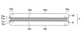
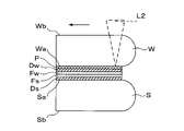
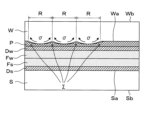
- a first wafer W as a first substrate and a second wafer S as a second substrate are joined together to form a superposed substrate.
- the process is performed on the superposed wafer T as . More specifically, as an example, in the superposed wafer T in which the first wafer W and the second wafer S are bonded, the peripheral edge portion We, which is a part of the first wafer W, is removed.
- the surface of the first wafer W to be bonded to the second wafer S will be referred to as a front surface Wa
- the surface opposite to the front surface Wa will be referred to as a rear surface Wb.
- the surface on the side bonded to the first wafer W is referred to as a front surface Sa
- the surface opposite to the front surface Sa is referred to as a rear surface Sb.
- the first wafer W is, for example, a semiconductor wafer such as a silicon substrate, and a device layer Dw including a plurality of devices is formed on the surface Wa side.
- a laser absorption film Fw is further formed on the device layer Dw, and is bonded to the second wafer S via the laser absorption film Fw.
- the laser absorption film Fw for example, an oxide film (THOX film, SiO2 film, TEOS film), SiC film, SiCN film, adhesive, or the like is used.
- the peripheral edge portion We of the first wafer W is chamfered, and the thickness of the cross section of the peripheral edge portion We decreases toward its tip. Further, the peripheral edge portion We is a portion to be removed in the edge trim described later, and is in the range of 0.5 mm to 3 mm in the radial direction from the outer end portion of the first wafer W, for example.
- the second wafer S has, for example, a device layer Ds and a bonding film Fs formed on its surface Sa, and is bonded to the first wafer W via the bonding film Fs. Further, the peripheral portion of the second wafer S is chamfered.
- the second wafer S does not have to be a device wafer on which the device layer Ds is formed, and may be a support wafer that supports the first wafer W, for example. In such a case, the second wafer S functions as a protective material that protects the device layer of the first wafer W.
- the first wafer W is bonded to the second wafer S via the laser absorption film Fw.
- a bonding film may be formed and used as the laser absorption film.
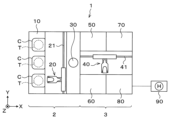
- the wafer processing system 1 has a configuration in which a loading/unloading station 2 and a processing station 3 are integrally connected.
- a cassette C capable of accommodating a plurality of superposed wafers T is loaded/unloaded to/from the outside.
- the processing station 3 includes various processing devices for performing desired processing on the superposed wafer T.
- the loading/unloading station 2 is provided with a cassette mounting table 10 on which a cassette C capable of accommodating a plurality of superposed wafers T is mounted.
- a wafer transfer device 20 is provided adjacent to the cassette mounting table 10 on the positive side of the cassette mounting table 10 in the X-axis direction.
- the wafer transfer device 20 is configured to move on a transfer path 21 extending in the Y-axis direction and transfer superimposed wafers T between a cassette C on the cassette mounting table 10 and a transition device 30 which will be described later.
- the loading/unloading station 2 is provided with a transition device 30 adjacent to the wafer transport device 20 on the X-axis positive direction side of the wafer transport device 20 and for transferring the overlapped wafers T to and from the processing station 3 . ing.
- a wafer transfer device 40 In the processing station 3, a wafer transfer device 40, an interface reforming device 50, an internal reforming device 60, a peripheral removal device 70 and a cleaning device 80 are arranged.
- the wafer transfer device 40 is provided on the side of the transition device 30 in the positive direction of the X axis.
- the wafer transfer device 40 is configured to be movable on a transfer path 41 extending in the X-axis direction, and includes the transition device 30 of the loading/unloading station 2, the interface reforming device 50, the internal reforming device 60, the edge removing device 70, and the cleaning device.
- the device 80 is configured so that the superposed wafer T can be transferred.
- the interface modification apparatus 50 irradiates a laser absorption film Fw formed at the interface between the first wafer W and the second wafer S with a laser beam (interface laser beam, for example, CO 2 laser), and the first wafer An unbonded area Ae is formed in which the bonding strength between W and the second wafer S is reduced.
- a laser beam interface laser beam, for example, CO 2 laser
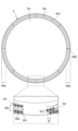
- the interface modification device 50 has a chuck 100 that holds the superposed wafer T on its upper surface.
- the chuck 100 holds the back surface Sb of the second wafer S by suction.
- the chuck 100 is supported by a slider table 102 via air bearings 101 .
- a rotating mechanism 103 is provided on the lower surface side of the slider table 102 .
- the rotation mechanism 103 incorporates, for example, a motor as a drive source.
- the chuck 100 is configured to be rotatable around the ⁇ axis (vertical axis) via an air bearing 101 by a rotating mechanism 103 .
- the slider table 102 is configured to be movable along a rail 105 extending in the Y-axis direction by means of a horizontal movement mechanism 104 provided on its underside. Rail 105 is provided on base 106 .
- the drive source for the horizontal movement mechanism 104 is not particularly limited, for example, a linear motor is used.
- a cooling mechanism 100a for cooling the superimposed wafer T sucked and held by the chuck 100 is provided inside the chuck 100.
- the structure of the cooling mechanism 100a is not particularly limited as long as it can appropriately cool the superposed wafer T (especially the vicinity of the portion irradiated with the laser light for the interface), and for example, a Peltier element or the like can be used.
- a laser irradiation system 110 is provided above the chuck 100 .
- a laser irradiation system 110 has a laser head 111 and a lens 112 .
- the lens 112 may be configured to be vertically movable by a lifting mechanism (not shown).
- the laser head 111 has a laser oscillator (not shown) that oscillates a pulsed laser beam. That is, the laser light irradiated from the laser irradiation system 110 to the superimposed wafer T held by the chuck 100 is a so-called pulse laser, and its power alternates between 0 (zero) and the maximum value. Also, in this embodiment, the laser light is CO 2 laser light, and the wavelength of the CO 2 laser light is, for example, 8.9 ⁇ m to 11 ⁇ m. Note that the laser head 111 may have a device other than the laser oscillator, such as an amplifier.
- the lens 112 is a cylindrical member and irradiates the superposed wafer T held by the chuck 100 with laser light.
- the laser light emitted from the laser irradiation system 110 passes through the first wafer W, is irradiated to the laser absorption film Fw, and is absorbed.
- the chuck 100 can be rotated and horizontally moved relative to the laser head 111 by the rotation mechanism 103 and the horizontal movement mechanism 104 . It may be configured to be relatively rotatable and horizontally movable. Also, both the chuck 100 and the laser head 111 may be configured to be relatively rotatable and horizontally movable.
- the laser head 111 may further have a spatial light modulator (not shown).
- the spatial light modulator modulates and outputs laser light.
- the spatial light modulator can control the focal position and phase of the laser light, and can adjust the shape and number (number of branches) of the irradiated laser light.
- the branched and irradiated laser light is configured so that the output, shape, etc. can be adjusted for each branch.
- the spatial light modulator for example, LCOS (Liquid Crystal Silicon) can be selected.
- the internal reforming device 60 irradiates the inside of the first wafer W with a laser beam (an internal laser beam, for example, a YAG laser) to form a peripheral modified layer M1, which serves as a starting point for separating the peripheral edge portion We, and a peripheral edge portion We.
- a divided modified layer M2 is formed as a starting point for breaking into small pieces.
- the configuration of the internal reformer 60 is not particularly limited.
- the internal reforming device 60 includes a chuck that holds the superimposed wafer T on its upper surface, a rotating mechanism that relatively rotates the chuck and the superposed wafer (first wafer W), and a chuck and the superposed wafer (first wafer W). W) relatively horizontally, and a laser irradiation unit (laser head) for irradiating the inside of the first wafer W held by the chuck with the internal laser light.
- the edge removal device 70 as a separation device removes the edge portion We of the first wafer W, that is, edge trims, with the modified edge layer M1 formed in the internal modification device 60 as a base point. Any method of edge trimming can be selected.
- the rim remover 70 may insert a blade between the first wafer W and the second wafer S, which may be wedge-shaped, for example. Further, for example, an air blow or a water jet may be injected toward the peripheral edge portion We to apply an impact to the peripheral edge portion We.
- the cleaning device 80 cleans the first wafer W and the second wafer S after edge trimming by the edge removing device 70 to remove particles on these wafers. Any washing method can be selected.
- a controller 90 is provided in the wafer processing system 1 described above.
- the control device 90 is, for example, a computer and has a program storage unit (not shown).
- the program storage unit stores programs for controlling the processing of the superposed wafers T in the wafer processing system 1 .
- the program storage unit also stores a program for controlling the operation of drive systems such as the above-described various processing devices and transfer devices to realize wafer processing, which will be described later, in the wafer processing system 1 .
- the program may be recorded in a computer-readable storage medium H and installed in the control device 90 from the storage medium H. Further, the storage medium H may be temporary or non-temporary.
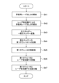
- the first wafer W and the second wafer S are joined to form a superimposed wafer T in advance.
- a cassette C containing a plurality of superposed wafers T is mounted on the cassette mounting table 10 of the loading/unloading station 2 .
- the superposed wafer T in the cassette C is taken out by the wafer transfer device 20 and transferred to the interface modification device 50 via the transition device 30 and the wafer transfer device 40 .
- the interface modification device 50 while rotating and moving the superposed wafer T (first wafer W) in the horizontal direction, the interface between the first wafer W and the second wafer S (more specifically, irradiates the above-mentioned laser absorption film Fw) formed on the interface with the interface laser light L2 in a pulsed manner. As a result, peeling occurs at the interface between the first wafer W and the second wafer S, as shown in FIG. 4(a).
- the bonding strength between the first wafer W and the second wafer S is lowered due to the separation at the interface between the first wafer W and the second wafer S.
- a junction region Ae is formed.
- a bonding area Ac is formed in which the two wafers S are bonded.
- edge trimming which will be described later, the peripheral edge portion We of the first wafer W to be removed is removed, but the presence of the unbonded region Ae in this way makes it possible to properly remove the peripheral edge portion We. can be done.
- the superposed wafer T on which the unbonded area Ae is formed is then transported to the internal reforming device 60 .
- the internal reforming device 60 irradiates the inside of the first wafer W with the internal laser beam L1 to form the peripheral reformed layer M1 and the divided reformed layers M2.
- the modified peripheral layer M1 serves as a base point for removing the peripheral edge portion We in edge trimming, which will be described later.
- the divided modified layer M2 serves as a starting point for dividing the peripheral portion We to be removed into small pieces. Note that in the drawings used for the following description, the illustration of the divided modified layer M2 may be omitted in order to avoid complication of the illustration.
- the superposed wafer T in which the modified edge layer M1 and the divided modified layer M2 are formed inside the first wafer W is then transferred to the edge removing apparatus 70 by the wafer transfer apparatus 40 .
- the peripheral edge removing device 70 removes the peripheral edge portion We of the first wafer W, that is, performs edge trimming.
- the peripheral edge portion We is separated from the central portion of the first wafer W (inside in the radial direction of the peripheral edge portion We) with the modified peripheral layer M1 as a starting point, and is separated from the second wafer with the unbonded area Ae as a starting point. completely separated from S.
- the peripheral portion We to be removed is divided into small pieces with the divided modified layer M2 as a base point.
- a wedge-shaped blade B (see FIG. 4(c)), for example, is inserted into the interface between the first wafer W and the second wafer S forming the superimposed wafer T. good too.
- the superposed wafer T from which the peripheral portion We of the first wafer W has been removed is then transferred to the cleaning device 80 by the wafer transfer device 40 .
- the cleaning device 80 cleans the first wafer W and/or the second wafer S from which the peripheral portion We has been removed.
- the first wafer W and the second wafer S are irradiated with a cleaning laser beam L3 to modify the irradiated portion of the laser beam. By removing, residual particles and the like may be removed (washed).
- the superposed wafer T that has undergone all the processes is transferred to the cassette C on the cassette mounting table 10 by the wafer transfer device 20 via the wafer transfer device 40 and the transition device 30 .
- the wafer transfer device 20 via the wafer transfer device 40 and the transition device 30 .
- the internal modification device 60 after forming the unbonded region Ae with the interface modification device 50, the internal modification device 60 performs the peripheral modified layer M1 and Although the split modified layer M2 is formed, the order of wafer processing in the wafer processing system 1 is not limited to this. That is, after the peripheral modified layer M1 and the divided modified layers M2 are formed by the internal modifying device 60, the unbonded area Ae may be formed by the interface modifying device 50.
- FIG. 4(a) and 4(b) after forming the unbonded region Ae with the interface modification device 50, the internal modification device 60 performs the peripheral modified layer M1 and Although the split modified layer M2 is formed, the order of wafer processing in the wafer processing system 1 is not limited to this. That is, after the peripheral modified layer M1 and the divided modified layers M2 are formed by the internal modifying device 60, the unbonded area Ae may be formed by the interface modifying device 50.
- the present inventors have discovered the possibility that the unbonded area Ae can be formed more preferably by controlling the temperature of the superposed wafer T during the irradiation of the interface laser beam L2 in the interface modification device 50. Found it. Therefore, in the wafer processing according to the present embodiment, the temperature of the superposed wafer T is controlled under various conditions in the interface modification device 50 to appropriately form the unbonded area Ae.
- the interface modification apparatus 50 first, as the layer information of the superposed wafer T on which the unbonded area Ae is to be formed, for example, the layer forming the peeling surface of the first wafer W (in this embodiment, for example, the laser absorption film Fw) to obtain the thickness and structure.
- the acquired layer information of the superposed wafer T is output to the control device 90 .
- the layer information of the polymerized wafer T may be obtained by the interface modification device 50 or may be previously obtained outside the interface modification device 50 . Further, the method of obtaining the layer information of the superimposed wafer T is not particularly limited.
- the inside of the superposed wafer T held by the chuck 100 which is the periphery of the first wafer W to be removed in this embodiment, is examined based on the acquired layer information.
- the interface laser beam L2 is applied to the laser absorption film Fw at the position corresponding to the portion We to form the unbonded region Ae.
- the laser absorption film Fw formed on the first wafer W is irradiated with the interface laser light L2 from the laser irradiation system 110.
- the irradiated interface laser light L2 is absorbed by the laser absorption film Fw.
- the laser absorption film Fw accumulates energy through absorption of the interface laser beam L2, so that the temperature rises and expands.
- shear stress occurs at the interface between the first wafer W and the laser absorption film Fw due to the expansion of the laser absorption film Fw.
- peeling occurs at the interface between the laser absorption film Fw and the bonding film Fs). That is, at the irradiation position of the interface laser beam L2, an unbonded area Ae is formed in which the bonding strength is lowered due to the peeling of the first wafer W and the second wafer S due to the peeling.
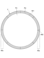
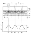
- the interface laser light L2 is applied to the laser absorption film Fw in a pulsed manner at a substantially constant irradiation pitch Q (physical irradiation interval of the interface laser light L2).
- the shear stress ⁇ generated at the interface between the first wafer W and the laser absorption film Fw is formed continuously with the temperature T1 of the region R1 immediately below which is directly irradiated with the interface laser beam L2 shown in FIG. It is considered that the larger the temperature difference ⁇ T between the temperature T2 of the peripheral region R2 between the one region R1 immediately below and the other region R1 directly below, the larger the temperature difference ⁇ T.
- the formation operation of the unbonded region Ae is controlled so that the temperature difference ⁇ T shown in FIG. It is considered that the peripheral portion We of the first wafer W can be appropriately removed.
- the controller 90 executes at least one of the following controls when forming the unbonded region Ae.
- the first control is a method of controlling the repetition frequency (hereinafter simply referred to as "frequency") of the interface laser light L2 with which the laser absorption film Fw is irradiated.
- the temperature of the laser absorption film Fw that has absorbed the interface laser beam L2 rises by accumulating energy.
- the temperature of the laser absorption film Fw as shown in FIG. 6, the temperature of the region R1 directly under the irradiation of the interface laser beam L2 rises significantly, and the temperature of the peripheral region R2 also rises.
- the interface laser for forming the other directly-underlying region R1 is emitted before the peripheral region R2, whose temperature rises due to the formation of the one directly-underlying region R1, is cooled.
- Light L2 is emitted. That is, when forming one directly-underlying region R1 and another directly-underlying region R1 adjacent to each other continuously, the temperature T2 of the peripheral region R2 between them may remain high, and the temperature difference ⁇ T may not be ensured.
- the frequency of the interface laser light L2 is changed based on the layer information of the superposed wafer T acquired prior to the irradiation of the interface laser light L2. More specifically, on the portion that is recognized to be difficult to peel based on the layer information (for example, the portion where the thickness of the laser absorption film Fw is large, or the portion having the film type of the laser absorption film Fw that is difficult to peel).
- the frequency of the interface laser beam L2 irradiated to the surface is made smaller than that of other portions where peeling can be performed normally.
- the temporal pulse interval of the interface laser beam L2 is increased (for example, by halving the frequency of the interface laser beam L2, the temporal pulse interval is increased). double).
- the temporal pulse interval of the interfacial laser beam L2 becomes longer, the natural cooling amount of the peripheral region R2 in the pulse interval increases. becomes lower, and the temperature difference ⁇ T shown in FIG. 6 can be increased.
- FIG. 7 is a table showing the delamination state of the first wafer W and the second wafer S when the unbonded area Ae is formed using the interface laser light L2 having different frequencies.
- the delamination states of the first wafer W and the second wafer S were checked when the frequency of the interface laser light L2 was set to 100 kHz and when the frequency was set to 50 kHz.
- the conditions other than the frequency of the interface laser light L2 for example, the thickness and structure as layer information of the laser absorption film Fw, the rotational speed of the superposed wafer T, etc.
- the irradiation pitch Q which is the physical irradiation interval of the interface laser light L2 is determined in advance. It is desirable to be controlled at a fixed constant value. In other words, it is desirable that the irradiation pitch Q between the difficult-to-separate portion obtained based on the layer information described above and the other normally-separable portion be controlled to be constant.
- the rotation speed of the superposed wafer T (corresponding to the irradiation pitch Q in the circumferential direction) is adjusted according to the frequency of the interface laser light L2. And it is desirable that the moving speed in the horizontal direction (corresponding to the irradiation pitch Q in the radial direction) is changed as appropriate. More specifically, when the frequency of the interface laser beam L2 is decreased, the rotational speed and the moving speed of the superposed wafer T are simultaneously decreased so that the irradiation pitch Q of the interface laser beam L2 is constant. Control is desirable.
- the frequency of the interface laser light L2 is lowered (lower frequency) or changed as appropriate, the first wafer W and the second wafer S are separated and the unbonded region Ae is properly formed. Although it can be formed, the time required to form the unbonded region Ae on the entire surface of the peripheral portion We increases.
- it is necessary to appropriately form the unbonded region Ae improve the throughput related to the formation of the unbonded region Ae, There is a trade-off relationship between In view of this point, it is desirable to irradiate the interface laser beam L2 at the minimum controllable frequency in consideration of the throughput in the interface modification device 50 .
- the frequency of the interface laser light L2 is reduced only in the portion where it is recognized that the separation of the first wafer W and the second wafer S is difficult, so that the unbonded region Ae is removed. is properly formed, and the frequency of the interface laser light L2 is returned (to a high frequency) in other portions where separation can be performed normally, thereby suppressing a decrease in throughput.
- the time required for the peripheral region R2, whose temperature has risen due to the formation of the one region R1, to cool to the temperature before the irradiation of the interface laser beam L2 does not depend on the frequency of the interface laser beam L2. It is presumed to be constant according to the energy amount of the interface laser light L2. In view of this point, the frequency of the interface laser light L2 is such that the temporal pulse interval of the interface laser light L2 is required for the peripheral region R2 to cool to the temperature before the irradiation of the interface laser light L2. It is desirable to be controlled so as to be substantially equal to or longer than the time.
- the laser head 111 has the above-described spatial light modulator (for example, LCOS), a plurality of different points on the laser absorption film Fw in plan view are simultaneously irradiated with the interface laser light L2. good too.
- a plurality of in-plane laser absorption films Fw simultaneously irradiated with the interface laser beam L2 are irradiated. It is desirable that the points (a plurality of condensing point positions) are arranged so as not to be adjacent to each other at least in the circumferential direction and the radial direction in plan view.
- a plurality of, in the illustrated example, two interface laser beams L2 are emitted at an irradiation pitch Q (see FIG. 6) of 2 in the circumferential direction of the superposed wafer T. Irradiate at twice the irradiation interval (one peripheral region R2 corresponding to one directly below region R1, with an interval of one size) to simultaneously form a plurality of one immediately below regions R1. good too.
- the condensing point positions of the plurality of interface laser beams L2 are sequentially shifted by the irradiation pitch Q in the circumferential direction, and the laser beams L2 are continuously irradiated.
- the first wafer W and the second wafer S are simultaneously peeled off at a plurality of points of the laser absorption film Fw in plan view, thereby improving the throughput related to the formation of the unbonded region Ae. can.
- the frequency of the interface laser light L2 based on the layer information of the superimposed wafer T as described above, when forming the plurality of other directly-underlying regions R1, one of the plurality of directly-underlying regions R1 and As a result, the temperature difference ⁇ T shown in FIG. 6 can be increased, and the unbonded area Ae can be properly formed.
- the arrangement of the plurality of interfacial laser beams L2 that are irradiated at the same time is not limited to the arrangement shown in FIG. 2, the two interface laser beams L2 may be arranged side by side with an interval (twice the irradiation pitch Q) in the radial direction of the superposed wafer T.
- FIG. 8B(b) a plurality of, in the illustrated example, two interface laser beams L2 are emitted at an irradiation interval of an irradiation pitch Q in both the radial direction and the circumferential direction of the superposed wafer T.
- a plurality of condensing points may be arranged obliquely in a plan view.
- the positions of the plurality of converging points are arranged so as not to be adjacent to each other in at least the circumferential direction and the radial direction in plan view of the laser absorbing film Fw, and the plurality of interface laser beams L2 are simultaneously irradiated.
- the temperature difference ⁇ T between the temperature T2 of the peripheral region R2 between the plurality of directly-underlying regions R1 and the plurality of other directly-underlying regions R1 can be increased.
- the unbonded areas Ae can be appropriately formed simultaneously at a plurality of points in plan view, and the throughput related to the formation of the unbonded areas Ae can be improved.
- the number of interface laser beams L2 that are irradiated at the same time is not limited to two, and three or more interface laser beams L2 may be simultaneously irradiated onto the laser absorption film Fw.
- the converging point positions of the three or more interface laser beams L2 may be arranged side by side at intervals in the circumferential direction, radial direction, or oblique direction of the superposed wafer T in a plan view, or may be arranged circumferentially. A combination of directional, radial or oblique arrangement may be used.
- the second control is a method of cooling the superimposed wafer T by a cooling mechanism 100 a arranged inside the chuck 100 .
- the shear stress ⁇ generated at the interface between the first wafer W and the laser absorption film Fw is considered to increase as the temperature difference ⁇ T between the temperature T1 of the directly-lower region R1 and the temperature T2 of the peripheral region R2 increases.
- the temperature T2 of the peripheral region R2 is lowered by cooling the superposed wafer T by the cooling mechanism 100a when the interface laser beam L2 is irradiated, thereby increasing the temperature difference ⁇ T shown in FIG. good too.
- cooling mechanism 100a is arranged inside the chuck 100 in the example shown in FIG. 3, the configuration and arrangement of the cooling mechanism 100a are not limited to this.
- cooling air is applied to the front surface of the superposed wafer T (back surface Wb of the first wafer W) as shown in FIG. 9A.
- An air nozzle 100b serving as a cooling mechanism that supplies air may be arranged.
- a cooling air supply source 113 is connected to the air nozzle 100b.
- the temperature of the cooling air Air is not particularly limited as long as it can cool the superposed wafer T and does not interfere with the irradiation of the interface laser beam L2. It may be at a low temperature below room temperature or at an extremely low temperature.
- the air nozzle 100b supplies cooling air Air from above to the central portion of the overlapped wafer T when irradiating the overlapped wafer T with the interface laser beam L2, and cools the entire surface of the overlapped wafer T by centrifugal force.
- the temperature T2 of the peripheral region R2 can be lowered, and the temperature difference ⁇ T shown in FIG. 6 can be increased.
- the irradiation position of the interface laser beam L2 may be determined based on the supply position of the cooling air Air.
- the interface laser beam L2 may be irradiated using the cooling air Air as a guide.
- the unbonded area Ae From the viewpoint of appropriately separating the first wafer W and the second wafer S to form the unbonded area Ae, at least the area directly under the irradiation of the interface laser beam L2 is required as described above. It is considered that the temperature difference ⁇ T between R1 and its peripheral region R2 should be increased. In other words, unlike the cooling mechanism 100a and the air nozzle 100b described above, it is not necessary to cool the entire surface of the superposed wafer T. If at least the peripheral region R2 in the vicinity of the vicinity of the irradiation of the interface laser beam L2 can be cooled, the unbonded state can be appropriately controlled. It is considered that the region Ae can be formed. From this point of view, a mechanism for locally cooling the peripheral region R2 may be provided instead of or in addition to the cooling mechanism 100a and the air nozzle 100b described above.
- an air nozzle 100c may be arranged as a cooling mechanism for supplying cooling air Air toward the peripheral region R2 when the superimposed wafer T is irradiated with the interface laser beam L2. good.
- a cooling air supply source 114 is connected to the air nozzle 100c.
- the air nozzle 100c that locally cools the peripheral region R2 may be configured integrally with the laser irradiation system 110 that irradiates the interface laser light L2 as shown in FIG. 9C.
- At least one of the above controls is executed by the control device 90, and the entire surface of the superposed wafer T at a position corresponding to the peripheral edge portion We of the first wafer W to be removed is to form an unbonded region Ae.
- the temperature difference ⁇ T between the temperature T1 of the region R1 directly under the irradiation of the interface laser beam L2 and the temperature T2 of the peripheral region R2 increases.
- Execute control Specifically, by controlling at least one of the frequency of the interface laser light L2 and the temperature of the superposed wafer T, the temperature T2 of the peripheral region R2 at the time of irradiation with the interface laser light L2 is reduced, thereby Increase the temperature difference ⁇ T.
- the laser absorption film Fw expands due to the absorption of the interface laser beam L2, thereby increasing the shear stress ⁇ generated between the directly-underlying region R1 and the peripheral region R2. can be properly separated from the wafer S.
- such temperature control can be applied to a portion of the peripheral portion We that is difficult to peel under normal high-frequency peeling conditions (irradiation conditions of the interface laser beam L2). run only.
- the first wafer W and the second wafer S can be appropriately separated from each other in the portion where separation is difficult under the normal separation conditions to form the unbonded region Ae, and normal separation can be performed in other portions.
- irradiating the interface laser light L2 under the conditions it is possible to suppress a decrease in throughput for forming the unbonded area Ae and improve the efficiency of forming the unbonded area Ae in the interface modification device 50 .
- a difficult-to-separate portion is detected based on layer information acquired in advance, and control is performed to increase the temperature difference ⁇ T with respect to the difficult-to-separate portion (temperature control of the superposed wafer T). and irradiation condition control of the interface laser beam L2) were executed.
- the interface modification apparatus 50 in addition to this, the first wafer W and the second wafer W are disposed radially inward (on the side where the modified edge layer M1 is formed) of the edge portion We where the processing quality of the edge trim is important.
- a similar control may be performed to properly delaminate the wafer S.
- the frequency of the interface laser light L2 (the temperature difference ⁇ T shown in FIG. 6) is controlled based on the radial position of the focal point of the interface laser light L2 in the plane of the superposed wafer T. you can go
- the first wafer W and the second wafer it is possible to properly remove S and improve the processing accuracy and processing quality of the edge trim.
- the frequency of the interface laser light L2 irradiated to the radially outer side of the peripheral edge portion We (the outer edge side of the first wafer W), which has little influence on the processing quality, is set to a high frequency (normal peeling conditions). By doing so, the throughput related to the formation of the unbonded area Ae can be improved.
- the laser absorption film Fw formed at the interface between the first wafer W and the second wafer S is irradiated with the interface laser light L2, and the laser absorption film
- the unbonded area Ae peeled surface
- the formation position of the unbonded area Ae is not limited to this as long as the peripheral edge portion We of the first wafer W can be removed appropriately.
- the unbonded area Ae is formed at the interface with weak bonding force between the first wafer W and the second wafer S. and the interface between the first wafer W and the device layer Dw, or the interface between the first wafer W and the device layer Ds.
- the bonding film Fs may be irradiated with the interface laser light L2 to form the unbonded region Ae.
- the unbonded area Ae is formed over the entire bonded interface between the first wafer W and the second wafer S in the superposed wafer T
- the unbonded area The first wafer W can be separated from the second wafer S appropriately by increasing the temperature difference ⁇ T between the directly-underlying region R1 and the peripheral region R2 when forming Ae.
- it is desirable that the frequency of the interface laser light L2 with which the interface between the first wafer W and the second wafer S is irradiated is determined based on layer information obtained in advance.
- the shape of the interface laser light L2 (shape of the condensing point) with which the interface between the first wafer W and the second wafer S is irradiated is not particularly limited.
- the shape of the focal point of the interface laser beam L2 is circular, as shown in FIG. A region that is not thermally affected by the interface laser beam L2 (white area in FIG. 11A: hereinafter referred to as “non-heating region R3”) is generated on the interface (laser absorption film Fw), and the non-heating region R3 has an appropriate
- the unbonded region Ae cannot be formed in the . Therefore, when the laser head 111 has the above-described spatial light modulator (for example, LCOS), the converging point shape of the interface laser light L2 should be controlled so as to reduce the area of the non-heating region R3. is desirable.
- the shape of the focal point of the interface laser beam L2 is a substantially trapezoidal shape having a shorter side on the radially inner side and a longer side on the radially outer side of the overlapped wafer T in plan view. It is desirable to control At this time, particularly when the unbonded area Ae is formed over the entire bonding interface between the first wafer W and the second wafer S, the length of the short side and/or the long side of the substantially trapezoidal shape is (Width of the trapezoidal shape) is desirably decreased as the irradiation position of the interface laser beam L2 goes radially inward of the superposed wafer T. As shown in FIG.
- the irradiation shape of the interface laser light L2 substantially trapezoidal in this way, the non-heating region R3 formed at the interface (laser absorption film Fw) between the first wafer W and the second wafer S is eliminated.
- the area can be reduced, and as a result, the entire surface of the peripheral edge portion We, which is the target for forming the unbonded region Ae, can be properly peeled off.
- the irradiation shape of the interface laser beam L2 is not limited to the shape shown in FIG. 11B.
- the short sides and/or long sides of the trapezoidal shape may have a curvature matching the concentric shape of the superposed wafer T (laser absorbing film Fw).
- the area of the non-heating region R3 can be further reduced.
- the irradiation shape of the interface laser light L2 is not limited to a substantially trapezoidal shape.
- the shapes (hexagons in the example shown) may be tiled, or they may be tiled with alternating triangles as shown in FIG. 11D.
- the laser absorption film Fw is an oxide film formed on the device layer Dw as shown in FIG. 1
- An absorbing film may be formed between the first wafer W and the device layer Dw. More specifically, as shown in FIG. 12, a laser absorption film P, a device layer Dw, and a bonding film F are laminated in this order on the surface Wa of the first wafer W, and the second wafer W is formed on the surface Wa. On the surface Sa of S, a device layer Ds and a bonding film Fs are laminated in this order.
- the laser absorption film P is, for example, an oxide film (SiO 2 film, TEOS film), and absorbs laser light in the same manner as the laser absorption film Fw described above.
- the device layers Dw, Ds include multiple devices.
- As the bonding films F and Fs for example, an oxide film (THOX film, SiO 2 film, TEOS film), SiC film, SiCN film, adhesive, or the like is used. W and a second wafer S are bonded.
- a method for removing the first wafer W from the second wafer S when the laser absorption film P for absorbing laser light is formed between the first wafer W and the device layer Dw will be described below. do.
- the case where the entire first wafer W is removed from the second wafer S as shown in FIG. A case of transferring to a wafer S of 1 is described as an example.
- the interface laser light L2 (CO 2 laser light) is irradiated in pulses (step St1 in FIG. 14).
- the interface laser beam L2 irradiated from the rear surface Wb side of the first wafer W passes through silicon (the first wafer W) and is absorbed by the laser absorption film P (see FIG. 13). 14 step St2).
- the interface laser light L2 absorbed by the laser absorption film P is converted into heat according to its energy distribution (step St3 in FIG. 14).
- the temperature of the laser absorption film P rises due to the absorption of the interface laser beam L2.
- Most of the heat (Ht in the figure) generated in the laser absorption film P by absorption of the interface laser beam L2 diffuses toward the first wafer W side as shown in FIG. St4).
- the temperature at the interface between the laser absorption film P and the first wafer W (silicon) rises.
- the influence of this heat that is, the temperature rise at the interface between the laser absorption film P and the first wafer W causes the interface as shown in FIG.
- the first wafer W in the irradiated portion of the laser beam L2 for laser beam L2 locally expands according to the temperature distribution (plastically deforms into a downward convex shape with respect to the laser absorption film P side) (step St5 in FIG. 14).
- the area affected by the heat generated by the irradiation of the interface laser beam L2 may be referred to as the "irradiation area R" of the interface laser beam L2.
- the first wafer W expands locally in the irradiation region R of the interface laser beam L2.
- the entire surface of the laser absorption film P in plan view is irradiated with the interface laser beam L2.
- the entire surface of the laser absorption film P is irradiated with the interface laser light L2 multiple times at intervals.
- the first wafer W locally expands each time it is irradiated with the laser beam L1, that is, a plurality of irradiation regions R are formed at intervals in different portions in plan view.
- the laser absorption film P is pressed from the upper side (the first wafer W side) along with the expansion of the first wafer W, and as a result, as shown in FIG.
- a compressive stress ⁇ 1 is generated in the laser absorption film P at the irradiation position of the interface laser beam L2.
- the generated compressive stress .sigma.1 acts in the direction in which the first wafer W and the laser absorption film P are separated (downward direction in the drawing, toward the laser absorption film P).
- a stress ⁇ 2 is generated.
- the generated compressive stress ⁇ 1 and peel stress ⁇ 2 are accumulated inside the laser absorbing film P.
- the peel stress ⁇ 2 generated in the plurality of irradiation regions R acts synergistically (overlappingly).
- the interface modification apparatus 50 causes the entire surface of the interface between the first wafer W and the laser absorption film P to delaminate in a plan view.
- the bonding strength is reduced over the entire surface of the first wafer W and the laser absorption film P.
- the first wafer W and the laser absorption film P can be properly separated in the subsequent separation step (step St7 in FIG. 14).
- the separation of the first wafer W from the laser absorption film P may be performed in a separation device (not shown) arranged in the wafer processing system 1, or may be performed inside the interface modification device 50. .
- a method for separating the first wafer W from the laser absorbing film P can be determined arbitrarily.
- the entire surface of the first wafer W is peeled off from the laser absorption film P.
- the irradiation region After peeling occurs at the edge Re of R, it is ideal that the first wafer W and the laser absorption film P are peeled off even in the central portion of the irradiation region R including the region directly under the irradiation due to the peeling stress ⁇ 2. .
- FIG. 1 shows that the first wafer W and the laser absorption film P are peeled off even in the central portion of the irradiation region R including the region directly under the irradiation due to the peeling stress ⁇ 2.
- a separation device (not shown) is provided, and a step of separating the first wafer W from the superimposed wafer T in the separation device is preferably provided.
- the ideal state described above that is, the laser absorption film P is formed on the entire surface of the first wafer W. If the superimposed wafer T is transferred to the separation position in a state in which separation is occurring, the first wafer W may fall from the second wafer S due to the inertial force or the like accompanying this transfer. Further, if the entire surface of the first wafer W is separated from the laser absorption film P in this way, it is not necessary to transport the superposed wafer T after the irradiation of the interface laser beam L2 to the separation position.
- the first wafer W may fly off the second wafer S due to the centrifugal force or the like accompanying the rotation of the chuck 100.
- an interface reforming apparatus is provided.
- the irradiation conditions of the interface laser light L2 irradiation position, output, etc.
- the first wafer W is completely separated from the laser absorption film P during irradiation with the interface laser beam L2 or during transportation to the separation position, and the second wafer may scatter and fall from the S. Suppressed.
- the device layer Dw formed on the first wafer W is transferred to the second wafer S as described above. That is, in the interface modification device 50, the first wafer W is expanded by the heat generated by the irradiation of the interface laser beam L2, and the compressive stress ⁇ 1 is generated in the laser absorption film P. A peeling stress ⁇ 2 is generated at the interface of the film P, causing peeling at the interface between the laser absorbing film P and the first wafer W, thereby reducing the bonding strength. Then, after the bonding strength is reduced over the entire surface of the laser absorption film P and the first wafer W, the first wafer W is lifted from the laser absorption film P in a separation device (not shown) or the interface modification device 50, for example. , the first wafer W is removed.
- the entire first wafer W is transferred to the second wafer.
- a part of the first wafer W may be removed from the second wafer S as well.
- the peripheral portion We may be removed from the second wafer S as a part of the first wafer W, that is, a so-called edge trimming process may be performed.
- Wafer processing system 50 Interface modification device 70 Edge removal device 90 Control device Ae Unbonded area Fw Laser absorption film L2 Interface laser light R1 Directly below area R2 Peripheral area S Second wafer T Superimposed wafer T1 Temperature (of directly below area) T2 temperature (of surrounding area) W first wafer ⁇ T temperature difference
Landscapes
- Laser Beam Processing (AREA)
- Mechanical Treatment Of Semiconductor (AREA)
Priority Applications (4)
| Application Number | Priority Date | Filing Date | Title |
|---|---|---|---|
| KR1020247007471A KR20240043781A (ko) | 2021-08-16 | 2022-07-27 | 처리 방법 및 처리 시스템 |
| JP2023542300A JP7678881B2 (ja) | 2021-08-16 | 2022-07-27 | 処理方法及び処理システム |
| CN202280055962.XA CN117795652A (zh) | 2021-08-16 | 2022-07-27 | 处理方法和处理系统 |
| JP2025076594A JP2025105952A (ja) | 2021-08-16 | 2025-05-02 | 処理方法及び処理システム |
Applications Claiming Priority (4)
| Application Number | Priority Date | Filing Date | Title |
|---|---|---|---|
| JP2021-132199 | 2021-08-16 | ||
| JP2021132199 | 2021-08-16 | ||
| JP2021-199502 | 2021-12-08 | ||
| JP2021199502 | 2021-12-08 |
Publications (1)
| Publication Number | Publication Date |
|---|---|
| WO2023021952A1 true WO2023021952A1 (ja) | 2023-02-23 |
Family
ID=85240587
Family Applications (1)
| Application Number | Title | Priority Date | Filing Date |
|---|---|---|---|
| PCT/JP2022/029027 Ceased WO2023021952A1 (ja) | 2021-08-16 | 2022-07-27 | 処理方法及び処理システム |
Country Status (4)
| Country | Link |
|---|---|
| JP (2) | JP7678881B2 (https=) |
| KR (1) | KR20240043781A (https=) |
| TW (1) | TW202314842A (https=) |
| WO (1) | WO2023021952A1 (https=) |
Cited By (2)
| Publication number | Priority date | Publication date | Assignee | Title |
|---|---|---|---|---|
| CN116364636A (zh) * | 2023-05-31 | 2023-06-30 | 广东鸿浩半导体设备有限公司 | 一种基于红外成像辅助的激光解键合方法 |
| WO2026079048A1 (ja) * | 2024-10-09 | 2026-04-16 | 東京エレクトロン株式会社 | 基板処理方法、プログラム、コンピュータ記憶媒体及び基板処理システム |
Citations (6)
| Publication number | Priority date | Publication date | Assignee | Title |
|---|---|---|---|---|
| JP2004111606A (ja) * | 2002-09-18 | 2004-04-08 | Tokyo Seimitsu Co Ltd | ウェーハの加工方法 |
| JP2020155493A (ja) * | 2019-03-18 | 2020-09-24 | キオクシア株式会社 | 半導体装置の製造方法および半導体装置 |
| WO2021010287A1 (ja) * | 2019-07-18 | 2021-01-21 | 東京エレクトロン株式会社 | 処理装置及び処理方法 |
| JP2021068869A (ja) * | 2019-10-28 | 2021-04-30 | 東京エレクトロン株式会社 | 基板処理方法及び基板処理システム |
| WO2021131711A1 (ja) * | 2019-12-26 | 2021-07-01 | 東京エレクトロン株式会社 | 基板処理方法及び基板処理装置 |
| JP2021103725A (ja) * | 2019-12-25 | 2021-07-15 | 東京エレクトロン株式会社 | 基板処理方法及び基板処理システム |
Family Cites Families (2)
| Publication number | Priority date | Publication date | Assignee | Title |
|---|---|---|---|---|
| US9214353B2 (en) * | 2012-02-26 | 2015-12-15 | Solexel, Inc. | Systems and methods for laser splitting and device layer transfer |
| CN118263105A (zh) | 2018-03-14 | 2024-06-28 | 东京毅力科创株式会社 | 基板处理系统、基板处理方法以及计算机存储介质 |
-
2022
- 2022-07-27 WO PCT/JP2022/029027 patent/WO2023021952A1/ja not_active Ceased
- 2022-07-27 JP JP2023542300A patent/JP7678881B2/ja active Active
- 2022-07-27 KR KR1020247007471A patent/KR20240043781A/ko active Pending
- 2022-08-08 TW TW111129669A patent/TW202314842A/zh unknown
-
2025
- 2025-05-02 JP JP2025076594A patent/JP2025105952A/ja active Pending
Patent Citations (6)
| Publication number | Priority date | Publication date | Assignee | Title |
|---|---|---|---|---|
| JP2004111606A (ja) * | 2002-09-18 | 2004-04-08 | Tokyo Seimitsu Co Ltd | ウェーハの加工方法 |
| JP2020155493A (ja) * | 2019-03-18 | 2020-09-24 | キオクシア株式会社 | 半導体装置の製造方法および半導体装置 |
| WO2021010287A1 (ja) * | 2019-07-18 | 2021-01-21 | 東京エレクトロン株式会社 | 処理装置及び処理方法 |
| JP2021068869A (ja) * | 2019-10-28 | 2021-04-30 | 東京エレクトロン株式会社 | 基板処理方法及び基板処理システム |
| JP2021103725A (ja) * | 2019-12-25 | 2021-07-15 | 東京エレクトロン株式会社 | 基板処理方法及び基板処理システム |
| WO2021131711A1 (ja) * | 2019-12-26 | 2021-07-01 | 東京エレクトロン株式会社 | 基板処理方法及び基板処理装置 |
Cited By (3)
| Publication number | Priority date | Publication date | Assignee | Title |
|---|---|---|---|---|
| CN116364636A (zh) * | 2023-05-31 | 2023-06-30 | 广东鸿浩半导体设备有限公司 | 一种基于红外成像辅助的激光解键合方法 |
| CN116364636B (zh) * | 2023-05-31 | 2023-07-28 | 广东鸿浩半导体设备有限公司 | 一种基于红外成像辅助的激光解键合方法 |
| WO2026079048A1 (ja) * | 2024-10-09 | 2026-04-16 | 東京エレクトロン株式会社 | 基板処理方法、プログラム、コンピュータ記憶媒体及び基板処理システム |
Also Published As
| Publication number | Publication date |
|---|---|
| KR20240043781A (ko) | 2024-04-03 |
| TW202314842A (zh) | 2023-04-01 |
| JPWO2023021952A1 (https=) | 2023-02-23 |
| JP7678881B2 (ja) | 2025-05-16 |
| JP2025105952A (ja) | 2025-07-10 |
Similar Documents
| Publication | Publication Date | Title |
|---|---|---|
| JP7720426B2 (ja) | 基板処理方法 | |
| KR101955067B1 (ko) | 개선된 핸들러 웨이퍼 탈착 방법 | |
| JP7133633B2 (ja) | 処理システム及び処理方法 | |
| JPWO2020017599A1 (ja) | 基板処理システム及び基板処理方法 | |
| JP7499845B2 (ja) | 基板処理方法及び基板処理装置 | |
| JP2025105952A (ja) | 処理方法及び処理システム | |
| JP7354420B2 (ja) | 基板処理方法及び基板処理装置 | |
| JP7607678B2 (ja) | 基板処理装置、基板処理方法及び基板製造方法 | |
| JP7577138B2 (ja) | 基板処理装置及び基板処理方法 | |
| JP7577137B2 (ja) | 基板処理装置及び基板処理方法 | |
| JPWO2023021952A5 (https=) | ||
| CN117795652A (zh) | 处理方法和处理系统 | |
| TW202404728A (zh) | 晶圓的加工方法 | |
| JP2023121926A (ja) | 処理方法及び処理システム | |
| JP7815447B2 (ja) | 基板処理システム、基板処理方法及びデバイス構造 | |
| JP7808697B2 (ja) | 基板処理装置及び基板処理方法 | |
| US20240128086A1 (en) | Method of processing wafer | |
| JP2025135546A (ja) | 剥離方法及び剥離システム | |
| TW202242163A (zh) | 濺射預處理方法 |
Legal Events
| Date | Code | Title | Description |
|---|---|---|---|
| 121 | Ep: the epo has been informed by wipo that ep was designated in this application |
Ref document number: 22858273 Country of ref document: EP Kind code of ref document: A1 |
|
| WWE | Wipo information: entry into national phase |
Ref document number: 2023542300 Country of ref document: JP |
|
| WWE | Wipo information: entry into national phase |
Ref document number: 202280055962.X Country of ref document: CN |
|
| WWE | Wipo information: entry into national phase |
Ref document number: 18683792 Country of ref document: US |
|
| NENP | Non-entry into the national phase |
Ref country code: DE |
|
| 122 | Ep: pct application non-entry in european phase |
Ref document number: 22858273 Country of ref document: EP Kind code of ref document: A1 |