WO2021010287A1 - 処理装置及び処理方法 - Google Patents
処理装置及び処理方法 Download PDFInfo
- Publication number
- WO2021010287A1 WO2021010287A1 PCT/JP2020/026891 JP2020026891W WO2021010287A1 WO 2021010287 A1 WO2021010287 A1 WO 2021010287A1 JP 2020026891 W JP2020026891 W JP 2020026891W WO 2021010287 A1 WO2021010287 A1 WO 2021010287A1
- Authority
- WO
- WIPO (PCT)
- Prior art keywords
- wafer
- layer
- internal surface
- processing
- modified
- Prior art date
Links
Images


Classifications
-
- H—ELECTRICITY
- H01—ELECTRIC ELEMENTS
- H01L—SEMICONDUCTOR DEVICES NOT COVERED BY CLASS H10
- H01L21/00—Processes or apparatus adapted for the manufacture or treatment of semiconductor or solid state devices or of parts thereof
- H01L21/02—Manufacture or treatment of semiconductor devices or of parts thereof
- H01L21/04—Manufacture or treatment of semiconductor devices or of parts thereof the devices having at least one potential-jump barrier or surface barrier, e.g. PN junction, depletion layer or carrier concentration layer
- H01L21/18—Manufacture or treatment of semiconductor devices or of parts thereof the devices having at least one potential-jump barrier or surface barrier, e.g. PN junction, depletion layer or carrier concentration layer the devices having semiconductor bodies comprising elements of Group IV of the Periodic System or AIIIBV compounds with or without impurities, e.g. doping materials
- H01L21/26—Bombardment with radiation
- H01L21/263—Bombardment with radiation with high-energy radiation
- H01L21/268—Bombardment with radiation with high-energy radiation using electromagnetic radiation, e.g. laser radiation
-
- H—ELECTRICITY
- H01—ELECTRIC ELEMENTS
- H01L—SEMICONDUCTOR DEVICES NOT COVERED BY CLASS H10
- H01L21/00—Processes or apparatus adapted for the manufacture or treatment of semiconductor or solid state devices or of parts thereof
- H01L21/70—Manufacture or treatment of devices consisting of a plurality of solid state components formed in or on a common substrate or of parts thereof; Manufacture of integrated circuit devices or of parts thereof
- H01L21/77—Manufacture or treatment of devices consisting of a plurality of solid state components or integrated circuits formed in, or on, a common substrate
- H01L21/78—Manufacture or treatment of devices consisting of a plurality of solid state components or integrated circuits formed in, or on, a common substrate with subsequent division of the substrate into plural individual devices
- H01L21/7806—Manufacture or treatment of devices consisting of a plurality of solid state components or integrated circuits formed in, or on, a common substrate with subsequent division of the substrate into plural individual devices involving the separation of the active layers from a substrate
-
- B—PERFORMING OPERATIONS; TRANSPORTING
- B23—MACHINE TOOLS; METAL-WORKING NOT OTHERWISE PROVIDED FOR
- B23K—SOLDERING OR UNSOLDERING; WELDING; CLADDING OR PLATING BY SOLDERING OR WELDING; CUTTING BY APPLYING HEAT LOCALLY, e.g. FLAME CUTTING; WORKING BY LASER BEAM
- B23K26/00—Working by laser beam, e.g. welding, cutting or boring
- B23K26/02—Positioning or observing the workpiece, e.g. with respect to the point of impact; Aligning, aiming or focusing the laser beam
- B23K26/06—Shaping the laser beam, e.g. by masks or multi-focusing
- B23K26/062—Shaping the laser beam, e.g. by masks or multi-focusing by direct control of the laser beam
-
- B—PERFORMING OPERATIONS; TRANSPORTING
- B23—MACHINE TOOLS; METAL-WORKING NOT OTHERWISE PROVIDED FOR
- B23K—SOLDERING OR UNSOLDERING; WELDING; CLADDING OR PLATING BY SOLDERING OR WELDING; CUTTING BY APPLYING HEAT LOCALLY, e.g. FLAME CUTTING; WORKING BY LASER BEAM
- B23K26/00—Working by laser beam, e.g. welding, cutting or boring
- B23K26/08—Devices involving relative movement between laser beam and workpiece
- B23K26/0823—Devices involving rotation of the workpiece
-
- B—PERFORMING OPERATIONS; TRANSPORTING
- B23—MACHINE TOOLS; METAL-WORKING NOT OTHERWISE PROVIDED FOR
- B23K—SOLDERING OR UNSOLDERING; WELDING; CLADDING OR PLATING BY SOLDERING OR WELDING; CUTTING BY APPLYING HEAT LOCALLY, e.g. FLAME CUTTING; WORKING BY LASER BEAM
- B23K26/00—Working by laser beam, e.g. welding, cutting or boring
- B23K26/08—Devices involving relative movement between laser beam and workpiece
- B23K26/083—Devices involving movement of the workpiece in at least one axial direction
- B23K26/0853—Devices involving movement of the workpiece in at least in two axial directions, e.g. in a plane
-
- B—PERFORMING OPERATIONS; TRANSPORTING
- B23—MACHINE TOOLS; METAL-WORKING NOT OTHERWISE PROVIDED FOR
- B23K—SOLDERING OR UNSOLDERING; WELDING; CLADDING OR PLATING BY SOLDERING OR WELDING; CUTTING BY APPLYING HEAT LOCALLY, e.g. FLAME CUTTING; WORKING BY LASER BEAM
- B23K26/00—Working by laser beam, e.g. welding, cutting or boring
- B23K26/50—Working by transmitting the laser beam through or within the workpiece
- B23K26/53—Working by transmitting the laser beam through or within the workpiece for modifying or reforming the material inside the workpiece, e.g. for producing break initiation cracks
-
- H—ELECTRICITY
- H01—ELECTRIC ELEMENTS
- H01L—SEMICONDUCTOR DEVICES NOT COVERED BY CLASS H10
- H01L21/00—Processes or apparatus adapted for the manufacture or treatment of semiconductor or solid state devices or of parts thereof
- H01L21/02—Manufacture or treatment of semiconductor devices or of parts thereof
- H01L21/04—Manufacture or treatment of semiconductor devices or of parts thereof the devices having at least one potential-jump barrier or surface barrier, e.g. PN junction, depletion layer or carrier concentration layer
- H01L21/18—Manufacture or treatment of semiconductor devices or of parts thereof the devices having at least one potential-jump barrier or surface barrier, e.g. PN junction, depletion layer or carrier concentration layer the devices having semiconductor bodies comprising elements of Group IV of the Periodic System or AIIIBV compounds with or without impurities, e.g. doping materials
- H01L21/30—Treatment of semiconductor bodies using processes or apparatus not provided for in groups H01L21/20 - H01L21/26
- H01L21/302—Treatment of semiconductor bodies using processes or apparatus not provided for in groups H01L21/20 - H01L21/26 to change their surface-physical characteristics or shape, e.g. etching, polishing, cutting
- H01L21/304—Mechanical treatment, e.g. grinding, polishing, cutting
-
- H—ELECTRICITY
- H01—ELECTRIC ELEMENTS
- H01L—SEMICONDUCTOR DEVICES NOT COVERED BY CLASS H10
- H01L21/00—Processes or apparatus adapted for the manufacture or treatment of semiconductor or solid state devices or of parts thereof
- H01L21/67—Apparatus specially adapted for handling semiconductor or electric solid state devices during manufacture or treatment thereof; Apparatus specially adapted for handling wafers during manufacture or treatment of semiconductor or electric solid state devices or components ; Apparatus not specifically provided for elsewhere
- H01L21/67005—Apparatus not specifically provided for elsewhere
- H01L21/67011—Apparatus for manufacture or treatment
- H01L21/67092—Apparatus for mechanical treatment
-
- B—PERFORMING OPERATIONS; TRANSPORTING
- B23—MACHINE TOOLS; METAL-WORKING NOT OTHERWISE PROVIDED FOR
- B23K—SOLDERING OR UNSOLDERING; WELDING; CLADDING OR PLATING BY SOLDERING OR WELDING; CUTTING BY APPLYING HEAT LOCALLY, e.g. FLAME CUTTING; WORKING BY LASER BEAM
- B23K2101/00—Articles made by soldering, welding or cutting
- B23K2101/36—Electric or electronic devices
- B23K2101/40—Semiconductor devices
-
- B—PERFORMING OPERATIONS; TRANSPORTING
- B23—MACHINE TOOLS; METAL-WORKING NOT OTHERWISE PROVIDED FOR
- B23K—SOLDERING OR UNSOLDERING; WELDING; CLADDING OR PLATING BY SOLDERING OR WELDING; CUTTING BY APPLYING HEAT LOCALLY, e.g. FLAME CUTTING; WORKING BY LASER BEAM
- B23K2103/00—Materials to be soldered, welded or cut
- B23K2103/50—Inorganic material, e.g. metals, not provided for in B23K2103/02 – B23K2103/26
- B23K2103/56—Inorganic material, e.g. metals, not provided for in B23K2103/02 – B23K2103/26 semiconducting
Definitions
- This disclosure relates to a processing apparatus and a processing method.
- Patent Document 1 discloses a method of forming an internal modified layer on a single crystal substrate and cutting the substrate with the internal modified layer as a base point.
- the internal modified layer is formed by irradiating the inside of a substrate with a laser beam to change a single crystal structure into a polycrystalline structure.
- adjacent processing marks are connected.
- the technology according to the present disclosure appropriately performs peripheral edge removal processing and separation processing of the processing object.
- One aspect of the present disclosure is a processing apparatus for processing a processing object, which comprises a modification portion that irradiates the inside of the processing object with a laser beam to form a plurality of modification layers along the plane direction.
- the control unit includes at least a control unit that controls the operation of the modification unit, and the control unit includes a peripheral modification layer that serves as a base point for peeling of the peripheral portion of the removal target of the processing target body, and the peripheral modification layer.
- a first inner surface modification layer formed in an annular shape concentric with the peripheral modification layer and a spiral inside the radial inside of the first inner surface modification layer.
- the modified portion is controlled so as to form a second internal surface modified layer.
- the peripheral edge removal process and the separation process of the object to be processed can be appropriately performed.
- a laser is formed inside a semiconductor wafer (hereinafter referred to as a wafer) such as a circular substrate in which devices such as a plurality of electronic circuits are formed on the surface.
- the wafer is thinned by irradiating light to form a modified layer and separating the wafer from the modified layer as a base point.
- the wafer on the front surface side on which the device is formed may be referred to as a "first separation wafer” and the back surface side may be referred to as a "second separation wafer”.
- an edge trim treatment is performed to prevent the peripheral edge of the wafer from becoming a sharp and sharp shape (so-called knife edge shape) due to the separation.
- the edge trim treatment is performed, for example, by irradiating the inside of the wafer with a laser beam along the peripheral edge portion to be removed to form a modified layer, and peeling the peripheral edge portion from the modified layer as a base point.
- the technique according to the present disclosure appropriately performs peripheral removal processing and separation processing of a processing object.
- a drawing is provided regarding a wafer processing system provided with the processing apparatus according to the present embodiment and a wafer processing method as a processing method. It will be explained with reference to it.
- elements having substantially the same functional configuration are designated by the same reference numerals to omit duplicate description.
- FIG. 1 is a plan view schematically showing an outline of the configuration of the wafer processing system 1.
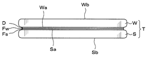
- the processing wafer W is separated and thinned.
- the surface on the side bonded to the support wafer S is referred to as a front surface Wa
- the surface opposite to the front surface Wa is referred to as a back surface Wb.
- the surface on the side joined to the processed wafer W is referred to as the front surface Sa
- the surface on the side opposite to the front surface Sa is referred to as the back surface Sb.
- the processed wafer W corresponds to the processed object in the present disclosure.
- the processed wafer W is, for example, a semiconductor wafer such as a silicon wafer having a disk shape, and a device layer D including a device such as a plurality of electronic circuits is formed on the surface Wa. Further, an oxide film Fw, for example, a SiO 2 film (TEOS film) is further formed on the device layer D.
- the processed wafer W constitutes the wafer as the separation target described above.
- the support wafer S is a wafer that supports the processed wafer W.
- An oxide film Fs for example, a SiO 2 film (TEOS film) is formed on the surface Sa of the support wafer S.
- TEOS film SiO 2 film
- a device layer (not shown) is formed on the surface Sa as in the processing wafer W.
- the device layer D and the oxide films Fw and Fs may be omitted in order to avoid the complexity of the illustration.
- the processed wafer W is subjected to an edge trim treatment to prevent the peripheral portion of the processed wafer W from becoming a knife edge shape due to the thinning treatment as described above.
- an edge trim treatment for example, as shown in FIG. 3, the peripheral edge modified layer M1 is formed by irradiating the boundary between the peripheral edge portion We and the central portion Wc as a removal target with a laser beam, and the peripheral edge modified layer M1 is formed. This is done by peeling the peripheral edge We from the base point.
- the peripheral edge portion We removed by the edge trim is, for example, in the range of 1 mm to 5 mm in the radial direction from the outer end portion of the processed wafer W. The method of edge trim processing will be described later.
- an unbonded region Ae for appropriately performing edge trim is formed at the interface between the processed wafer W and the support wafer S in the portion corresponding to the peripheral edge portion We as the removal target in the edge trim.
- a bonding region Ac in which the processing wafer W and the supporting wafer S are bonded and a bonding between the processing wafer W and the supporting wafer S are performed. It forms an unbonded region Ae with reduced strength. It is preferable that the outer end portion of the joint region Ac is located slightly radially outward from the inner end portion of the peripheral edge portion We to be removed.
- the unbonded region Ae may be formed, for example, before joining. Specifically, the bonding interface of the processed wafer W before bonding is reduced in bonding strength by removing it by polishing or wet etching, modifying it by irradiating it with a laser beam, or making it hydrophobic by applying a hydrophobic material. An unbonded region Ae can be formed.
- the "bonding interface" on which the unbonded region Ae is formed refers to a portion of the processed wafer W that forms an interface that is actually bonded to the support wafer S.
- the unbonded region Ae may be formed after joining, for example. Specifically, it is formed by irradiating the interface at the peripheral portion We of the processed wafer W after bonding with a laser beam to reduce the bonding strength of the support wafer S with respect to the surface Sa. If the unbonded region Ae can appropriately reduce the bonding force between the processed wafer W and the supporting wafer S at the peripheral edge of the processed wafer W, the unbonded region is near the bonding interface between the processed wafer W and the supporting wafer S. Can be formed in any position of. That is, the "near the bonding interface" according to the present embodiment includes the inside of the processed wafer W, the inside of the device layer D, the inside of the oxide film Fw, and the like.
- the wafer processing system 1 has a configuration in which the loading / unloading station 2 and the processing station 3 are integrally connected.
- the carry-in / out station 2 carries in / out a cassette Ct capable of accommodating a plurality of polymerized wafers T with, for example, the outside.
- the processing station 3 is provided with various processing devices for processing the polymerized wafer T.
- the loading / unloading station 2 is provided with a cassette mounting stand 10.
- a cassette mounting stand 10 In the illustrated example, a plurality of, for example, three cassettes Ct can be freely mounted in a row on the cassette mounting table 10 in the Y-axis direction.
- the number of cassettes Ct mounted on the cassette mounting table 10 is not limited to this embodiment and can be arbitrarily determined.
- the loading / unloading station 2 is provided with a wafer transfer device 20 adjacent to the cassette mounting table 10 on the X-axis negative direction side of the cassette mounting table 10.
- the wafer transfer device 20 is configured to be movable on a transfer path 21 extending in the Y-axis direction. Further, the wafer transfer device 20 has, for example, two transfer arms 22 and 22 that hold and transfer the polymerized wafer T.
- Each transport arm 22 is configured to be movable in the horizontal direction, the vertical direction, the horizontal axis, and the vertical axis.
- the configuration of the transport arm 22 is not limited to this embodiment, and any configuration can be adopted.
- the wafer transfer device 20 is configured to be able to transfer the polymerized wafer T to the cassette Ct of the cassette mounting table 10 and the transition device 30 described later.
- the loading / unloading station 2 is provided with a transition device 30 for delivering the polymerized wafer T adjacent to the wafer transfer device 20 on the X-axis negative direction side of the wafer transfer device 20.
- the processing station 3 is provided with, for example, three processing blocks G1 to G3.
- the first processing block G1, the second processing block G2, and the third processing block G3 are arranged side by side in this order from the X-axis positive direction side (import / export station 2 side) to the negative direction side.
- the first processing block G1 is provided with an etching device 40, a cleaning device 41, and a wafer transfer device 50.
- the etching apparatus 40 and the cleaning apparatus 41 are arranged in a laminated manner.
- the number and arrangement of the etching apparatus 40 and the cleaning apparatus 41 are not limited to this.
- the etching apparatus 40 and the cleaning apparatus 41 may be placed side by side in the X-axis direction. Further, the etching apparatus 40 and the cleaning apparatus 41 may be laminated respectively.
- the etching apparatus 40 etches the separated surface of the processed wafer W ground by the processing apparatus 80 described later.
- a chemical solution etching solution
- the separation surface is wet-etched.
- the chemical solution for example, HF, HNO 3 , H 3 PO 4 , TMAH, Choline, KOH and the like are used.
- the cleaning device 41 cleans the separation surface of the processed wafer W ground by the processing device 80 described later. For example, a brush is brought into contact with the separation surface to scrub clean the separation surface. A pressurized cleaning liquid may be used for cleaning the separation surface. Further, the cleaning device 41 may have a configuration for cleaning the back surface Sb of the support wafer S together with the separation surface of the processing wafer W.
- the wafer transfer device 50 is arranged, for example, on the Y-axis negative direction side of the etching device 40 and the cleaning device 41.
- the wafer transfer device 50 has, for example, two transfer arms 51, 51 that hold and transfer the polymerized wafer T.
- Each transport arm 51 is configured to be movable in the horizontal direction, the vertical direction, the horizontal axis, and the vertical axis.
- the configuration of the transport arm 51 is not limited to this embodiment, and any configuration can be adopted.
- the wafer transfer device 50 is configured to be able to transfer the polymerized wafer T to the transition device 30, the etching device 40, the cleaning device 41, and the reforming device 60 described later.
- the second processing block G2 is provided with a reformer 60 and a wafer transfer device 70 as processing devices.
- the number and arrangement of the reforming devices 60 are not limited to this embodiment, and a plurality of reforming devices 60 may be stacked and arranged.
- the reformer 60 irradiates the inside of the processed wafer W with laser light to form an unbonded region Ae, a peripheral reforming layer M1, an internal surface reforming layer M2, and a central reforming layer M3.
- the detailed configuration of the reformer 60 will be described later.
- the wafer transfer device 70 is arranged, for example, on the Y-axis positive direction side of the reformer 60.
- the wafer transfer device 70 has, for example, two transfer arms 71 and 71 that hold and transfer the polymerized wafer T.
- Each transport arm 71 is supported by an articulated arm member 72, and is configured to be movable in the horizontal direction, the vertical direction, the horizontal axis, and the vertical axis.
- the configuration of the transport arm 71 is not limited to this embodiment, and any configuration can be adopted.
- the wafer transfer device 70 is configured to be able to transfer the polymerized wafer T to the cleaning device 41, the reforming device 60, and the processing device 80 described later.
- the processing device 80 is provided in the third processing block G3.
- the number and arrangement of the processing devices 80 are not limited to this embodiment, and a plurality of processing devices 80 may be arbitrarily arranged.
- the processing device 80 has a rotary table 81.
- the rotary table 81 is rotatably configured around a vertical rotation center line 82 by a rotation mechanism (not shown).
- Two chucks 83 for sucking and holding the polymerized wafer T are provided on the rotary table 81.
- the chucks 83 are evenly arranged on the same circumference as the rotary table 81.
- the two chucks 83 can be moved to the delivery position 80a and the processing position 80b by rotating the rotary table 81.
- each of the two chucks 83 is configured to be rotatable around a vertical axis by a rotation mechanism (not shown).
- a grinding unit 84 is arranged at the processing position 80b to grind the processed wafer W.
- the grinding unit 84 has a grinding unit 85 having an annular shape and a rotatable grinding wheel (not shown). Further, the grinding portion 85 is configured to be movable in the vertical direction along the support column 86. Then, with the processed wafer W held by the chuck 83 in contact with the grinding wheel, the chuck 83 and the grinding wheel are rotated, respectively.
- the above wafer processing system 1 is provided with a control device 90 as a control unit.
- the control device 90 is, for example, a computer equipped with a CPU, a memory, or the like, and has a program storage unit (not shown).
- the program storage unit stores a program that controls the processing of the processing wafer W in the wafer processing system 1. Further, the program storage unit also stores a program for controlling the operation of the drive system of the above-mentioned various processing devices and transfer devices to realize the wafer processing described later in the wafer processing system 1.
- the program may be recorded on a computer-readable storage medium H and may be installed on the control device 90 from the storage medium H.
- control devices for independently controlling the various processing devices.
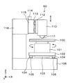
- 4 and 5 are a plan view and a side view showing an outline of the configuration of the reformer 60, respectively.
- the reformer 60 has a chuck 100 as a holding portion that holds the polymerized wafer T on the upper surface.
- the chuck 100 attracts and holds the back surface Sb of the support wafer S in a state where the processing wafer W is on the upper side and the support wafer S is arranged on the lower side.
- the chuck 100 is supported by the slider table 102 via an air bearing 101.
- a rotation mechanism 103 is provided on the lower surface side of the slider table 102.
- the rotation mechanism 103 has, for example, a built-in motor as a drive source.
- the chuck 100 is rotatably configured around a vertical axis by a rotation mechanism 103 via an air bearing 101.
- the slider table 102 is configured to be movable along a rail 105 provided on the base 106 and extending in the Y-axis direction via a moving mechanism 104 as a holding portion moving mechanism provided on the lower surface side thereof.
- the drive source of the moving mechanism 104 is not particularly limited, but for example, a linear motor is used.
- a laser head 110 as a reforming portion is provided above the chuck 100.
- the laser head 110 has a lens 111.
- the lens 111 is a tubular member provided on the lower surface of the laser head 110, and irradiates the processed wafer W held by the chuck 100 with laser light.
- the laser head 110 is a high-frequency pulsed laser beam oscillated from a laser beam oscillator (not shown), and emits a laser beam having a wavelength that is transparent to the processing wafer W inside the processing wafer W.
- the light is focused and irradiated at a predetermined position.
- the portion of the treated wafer W where the laser light is focused is modified to form the unbonded region Ae, the peripheral modification layer M1, the inner surface modification layer M2, and the central modification layer M3.
- the unbonded region Ae, the peripheral modified layer M1, the inner surface modified layer M2, and the central modified layer M3 are formed by a common laser head 110.
- they may be formed by different laser heads.
- the laser head may be used properly depending on the type of laser light to be irradiated.
- the laser head 110 is supported by the support member 112.
- the laser head 110 is configured to be vertically elevated by an elevating mechanism 114 along a rail 113 extending in the vertical direction. Further, the laser head 110 is configured to be movable in the Y-axis direction by a moving mechanism 115 as a reforming portion moving mechanism.
- the elevating mechanism 114 and the moving mechanism 115 are each supported by the support pillar 116.
- a macro camera 120 and a micro camera 121 are provided above the chuck 100 and on the Y-axis positive direction side of the laser head 110.
- the macro camera 120 and the micro camera 121 are integrally configured, and the macro camera 120 is arranged on the Y-axis positive direction side of the micro camera 121.
- the macro camera 120 and the micro camera 121 are configured to be vertically movable by the elevating mechanism 122, and further configured to be movable in the Y-axis direction by the moving mechanism 123.
- the macro camera 120 captures an image of the outer end of the processed wafer W (polymerized wafer T).
- the macro camera 120 includes, for example, a coaxial lens, irradiates visible light, for example, red light, and further receives reflected light from an object.
- the imaging magnification of the macro camera 120 is 2 times.
- the image captured by the macro camera 120 is output to the control device 90.
- the control device 90 calculates the first eccentricity amount of the center of the chuck 100 and the center of the processing wafer W from the image captured by the macro camera 120.
- the micro camera 121 images the peripheral edge of the processed wafer W and images the boundary between the bonded region Ac and the unbonded region Ae.
- the microcamera 121 includes, for example, a coaxial lens, irradiates infrared light (IR light), and further receives reflected light from an object.
- IR light infrared light
- the imaging magnification of the micro camera 121 is 10 times, the field of view is about 1/5 of that of the macro camera 120, and the pixel size is about 1/5 of that of the macro camera 120.
- the image captured by the micro camera 121 is output to the control device 90.
- the control device 90 calculates the second eccentricity amount between the center of the chuck 100 and the center of the junction region Ac from the image captured by the micro camera 121. Further, the control device 90 moves the chuck 100 or the laser head 110 so that the center of the chuck 100 and the center of the junction region Ac coincide with each other based on the second eccentricity amount.
- the control for moving the chuck 100 or the laser head 110 may be referred to as eccentricity correction.
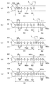
- FIG. 6 is a flow chart showing a main process of wafer processing.
- FIG. 7 is an explanatory diagram of a main process of wafer processing.
- the processing wafer W and the support wafer S are bonded to each other in an external bonding device (not shown) of the wafer processing system 1 to form a polymerized wafer T in advance.
- the unbonded region Ae described above may be formed in advance on the polymerization wafer T carried into the wafer processing system 1, but in the following description, when the unbonded region Ae is formed in the reformer 60. Will be explained as an example.
- the cassette Ct containing a plurality of the polymerization wafers T shown in FIG. 7A is placed on the cassette mounting table 10 of the loading / unloading station 2.
- the polymerized wafer T in the cassette Ct is taken out by the wafer transfer device 20 and transferred to the transition device 30.
- the wafer transfer device 50 takes out the polymerized wafer T of the transition device 30 and transfers it to the reformer 60.
- the reformer 60 first, an unbonded region Ae is formed as shown in FIG. 7 (b) (step A1 in FIG. 6).
- the peripheral modification layer M1 is formed inside the processed wafer W as shown in FIG. 7C (step A2 in FIG. 6), and the internal surface modification layer M2 is formed as shown in FIG. 7D. It is formed (step A3 in FIG. 6), and a central modified layer M3 is further formed (step A4 in FIG. 6).
- the peripheral edge modification layer M1 serves as a base point when the peripheral edge portion We is removed in the edge trim.
- the internal surface modification layer M2 serves as a base point for separating the processed wafer W.
- the central reforming layer M3 controls the growth of cracks in the central portion of the processed wafer W and serves as a starting point for separation in the central portion of the processed wafer W.
- the polymerized wafer T is carried into the reformer 60 by the wafer transfer device 50 and held by the chuck 100.
- the chuck 100 is moved to the formation position of the unbonded region Ae.
- the unbonded region Ae is formed at a position where the laser head 110 can irradiate the peripheral portion We of the processing wafer W with the laser beam.
- the unbonded region Ae is formed by irradiating the laser beam L (for example, CO 2 laser) from the laser head 110 while rotating the chuck 100 in the circumferential direction (step A1 in FIG. 6).
- the unbonded region Ae can be formed at an arbitrary position near the bonding interface as long as the bonding strength between the processed wafer W and the supporting wafer S can be reduced.
- the macro alignment position is a position where the macro camera 120 can image the outer end portion of the processing wafer W.
- the macro camera 120 captures an image of the outer end portion of the processed wafer W at 360 degrees in the circumferential direction.
- the captured image is output from the macro camera 120 to the control device 90.
- the control device 90 calculates the first eccentricity amount of the center of the chuck 100 and the center of the processing wafer W from the image of the macro camera 120. Further, the control device 90 calculates the movement amount of the chuck 100 so as to correct the Y-axis component of the first eccentric amount based on the first eccentric amount.
- the chuck 100 moves in the Y-axis direction based on the calculated movement amount, and moves the chuck 100 to the micro-alignment position.
- the micro-alignment position is a position where the micro camera 121 can image the peripheral edge of the processing wafer W.
- the field of view of the micro camera 121 is as small as about 1/5 of that of the macro camera 120.
- the peripheral edge of the processing wafer W is the micro camera. It may not fit in the angle of view of 121 and cannot be imaged by the micro camera 121. Therefore, it can be said that the correction of the Y-axis component based on the first eccentricity amount is for moving the chuck 100 to the micro-alignment position.
- the boundary between the bonded region Ac and the unbonded region Ae at 360 degrees in the circumferential direction of the processed wafer W is imaged by the micro camera 121.
- the captured image is output from the micro camera 121 to the control device 90.
- the control device 90 calculates the second eccentricity between the center of the chuck 100 and the center of the junction region Ac from the image of the micro camera 121. Further, the control device 90 determines the position of the chuck 100 with respect to the peripheral modification layer M1 so that the center of the bonding region Ac and the center of the chuck 100 coincide with each other based on the second eccentricity amount.
- the modification position is a position where the laser head 110 irradiates the processed wafer W with laser light to form the peripheral modification layer M1.
- the modification position is the same as the micro-alignment position.
- a laser beam L (for example, a YAG laser) is irradiated from the laser head 110 to form a peripheral modification layer M1 at the boundary between the peripheral portion We and the central portion Wc of the processed wafer W.
- a laser beam L for example, a YAG laser
- Step A2 in FIG. 6 a laser beam L (for example, a YAG laser) is irradiated from the laser head 110 to form a peripheral modification layer M1 at the boundary between the peripheral portion We and the central portion Wc of the processed wafer W.
- the lower end of the peripheral modification layer M1 formed by the laser beam L is located above the surface of the processed wafer W after separation after the final finishing process. That is, the formation position is adjusted so that the peripheral modification layer M1 does not remain on the first separation wafer W1 after separation (more specifically, after the grinding process described later).
- step A2 the chuck 100 is rotated by the rotating mechanism 103 and the moving mechanism 104 so that the center of the joining region Ac and the center of the chuck 100 coincide with the position of the chuck 100 determined by the control device 90.
- the chuck 100 is moved in the Y-axis direction (eccentricity correction). At this time, the rotation of the chuck 100 and the movement in the Y-axis direction are synchronized.
- the laser beam L is irradiated from the laser head 110 to the inside of the processed wafer W. That is, the peripheral modification layer M1 is formed while correcting the second eccentricity amount. Then, the peripheral modification layer M1 is formed in an annular shape concentric with the bonding region Ac. Therefore, after that, the peripheral edge portion We can be appropriately removed with the peripheral edge modifying layer M1 (crack C1) as a base point.
- the chuck 100 when the second eccentricity amount includes the X-axis component, the chuck 100 is rotated while moving the chuck 100 in the Y-axis direction to correct the X-axis component.
- the second eccentricity amount when the second eccentricity amount does not include the X-axis component, it is sufficient to move the chuck 100 in the Y-axis direction without rotating it.
- laser light L (for example, a YAG laser) is irradiated from the laser head 110 to form an internal surface modification layer M2 along the surface direction (step A3 in FIG. 6).
- the black arrow shown in FIG. 11 indicates the rotation direction of the chuck 100, and the white arrow indicates the moving direction of the processing point due to the movement of the chuck 100 or the laser head 110.
- cracks C2 grow in the plane direction from the internal surface modification layer M2.
- the crack C2 grows only on the radial inside of the peripheral modification layer M1.
- the quality of the edge trim after the peripheral edge We is removed is deteriorated as shown in FIG. That is, the peripheral edge portion We may not be properly removed with the peripheral edge modifying layer M1 (crack C1) as a base point, and a part of the peripheral edge portion We may remain on the support wafer S. From this point of view, the formation position of the inner surface modification layer M2 is adjusted so as to be formed radially inside the peripheral modification layer M1.
- the lower end of the internal surface modification layer M2 formed by the laser beam L is located above the surface of the processed wafer W after separation after the final finishing process. That is, the formation position is adjusted so that the internal surface modification layer M2 does not remain on the first separation wafer after separation (more specifically, after the grinding process described later).
- step A3 the chuck 100 (processed wafer W) is rotated, and the laser head 110 is moved from the outside in the radial direction to the inside in the Y-axis direction of the processed wafer W from the laser head 110 to the inside of the processed wafer W.
- the inner surface modification layer M2 spirally formed in the surface direction is formed. The details of the method for forming the internal surface modification layer M2 will be described later.
- the chuck 100 or the laser head 110 is moved in the Y-axis direction when the internal surface modification layer M2 is formed, but the same member as the chuck 100 or the laser head 110 that is moved in the eccentricity correction. To move. That is, in forming the inner surface modified layer M2, the eccentricity correction and the formation of the inner surface modified layer M2 are simultaneously controlled uniaxially as described later. Further, although the chuck 100 is rotated in forming the internal surface modification layer M2, the laser head 110 may be moved to rotate the laser head 110 relative to the chuck 100.
- the rotation speed of the chuck 100 and the frequency of the laser beam L are controlled to adjust the spacing between the internal surface modification layers M2. That is, when the radial position of the laser head 110 (irradiation position of the laser beam L) is on the outer peripheral portion of the processing wafer W, the rotation speed is slowed down, and when the radial position of the laser head 110 is in the central portion. The rotation speed is increased.
- the frequency is increased, and when the radial position of the laser head 110 is on the central portion, the frequency is increased. Is made smaller.
- the laser head 110 is then irradiated with laser light L (for example, a YAG laser) as shown in FIG. 13, and center modification is performed along the surface direction.
- Layer M3 is formed (step A4 in FIG. 6). Inside the processed wafer W, cracks C3 grow in the plane direction from the central modified layer M3.
- the central modified layer M3 is formed so as to be separated from each other (for example, 10 ⁇ m or more) so that the cracks C3 are not connected to each other and are not connected to the cracks C2.
- step A4 the rotation of the chuck 100 (processed wafer W) is stopped, and the laser head 110 is moved above the processed wafer W in the horizontal direction (X-axis direction, Y-axis direction) from the laser head 110 to the processed wafer W.
- the laser head 110 is moved above the processed wafer W in the horizontal direction (X-axis direction, Y-axis direction) from the laser head 110 to the processed wafer W.
- a central modified layer M3 linear in the plane direction is formed. Details of the method for forming the central modified layer M3 in step A4 will be described later.
- the chuck 100 may be moved in the horizontal direction instead of moving the laser head 110 in the horizontal direction.
- the polymerized wafer T is then carried out from the reforming device 60 by the wafer transfer device 70.
- the polymerized wafer T is transferred to the processing device 80 by the wafer transfer device 70.
- the processing apparatus 80 first, when the polymerized wafer T is delivered from the transport arm 71 to the chuck 83, the processed wafer W is based on the peripheral modification layer M1 and the internal surface modification layer M2 as shown in FIG. 7 (e). Is separated into a first separation wafer W1 and a second separation wafer W2 (step A5 in FIG. 6). At this time, the peripheral portion We is also removed from the processed wafer W. At this time, since the unbonded region Ae is formed in the vicinity of the bonding interface between the processed wafer W and the supporting wafer S, the peripheral portion We can be easily peeled off, so that the processed wafer W is appropriately separated. Can be done.
- step A5 as shown in FIG. 14A, the processing wafer W is sucked and held by the suction surface 71a provided on the transport arm 71, and the support wafer S is sucked and held by the chuck 83.
- the transfer arm 71 is raised to the first separation wafer W1 and the second separation wafer W2 in a state where the suction surface 71a sucks and holds the back surface Wb of the processing wafer W.
- the second separated wafer W2 is integrally separated from the peripheral edge portion We, that is, the peripheral portion We is removed and the processed wafer W is separated (thinned) at the same time.
- the separated second separated wafer W2 is recovered to the outside of the wafer processing system 1, for example. Further, for example, a recovery unit (not shown) is provided within the movable range of the transport arm 71, and the collection unit releases the adsorption of the second separation wafer W2 to recover the separated second separation wafer W2. You may.
- the processing wafer W is separated by using the wafer transfer device 70 in the processing device 80, but the wafer processing system 1 is provided with a separation device (not shown) for separating the processed wafer W. It may have been.
- the separating device can be arranged so as to be laminated with the reforming device 60, for example.
- the chuck 83 is moved to the processing position 80b.
- the grinding unit 84 grinds the back surface W1b, which is the separation surface of the first separation wafer W1 held by the chuck 83, and the peripheral edge modification layer M1 remaining on the back surface W1b,
- the inner surface modification layer M2 and the center modification layer M3 are removed (step A6 in FIG. 6).
- step A6 with the grinding wheel in contact with the back surface W1b, the first separation wafer W1 and the grinding wheel are each rotated to grind the back surface W1b.
- the back surface W1b of the first separation wafer W1 may be cleaned with the cleaning liquid using a cleaning liquid nozzle (not shown).
- the polymerized wafer T is transferred to the cleaning device 41 by the wafer transfer device 70.
- the back surface W1b which is the separation surface of the first separation wafer W1
- the back surface Sb of the support wafer S may be cleaned together with the back surface W1b of the first separation wafer W1.
- the polymerized wafer T is transferred to the etching device 40 by the wafer transfer device 50.
- the back surface W1b of the first separation wafer W1 which is the separation surface is wet-etched by the chemical solution (step A8 in FIG. 6). Grinding marks may be formed on the back surface W1b ground by the processing device 80 described above. In step A8, the grinding marks can be removed by wet etching to smooth the back surface W1b.
- the polymerized wafer T that has been subjected to all the processing is transported to the transition device 30 by the wafer transfer device 50, and further transferred to the cassette Ct of the cassette mounting table 10 by the wafer transfer device 20. In this way, a series of wafer processing in the wafer processing system 1 is completed.
- the processing order of steps A1 to A8 can be changed as appropriate.
- the order of forming the peripheral modification layer M1 in step A2 and the formation of the internal surface modification layer M2 in step A3 may be changed.
- the wafer processing is performed in the order of step A1, step A3, step A2, and steps A4 to A8.
- the formation of the central modified layer M3 in step A4 may be performed before the formation of the peripheral modified layer M1 in step A2.
- the wafer processing is performed in the order of step A1, step A4, steps A2 to A3, and steps A5 to A8.
- the formation of the central modified layer M3 in step A4 may be performed before the formation of the inner surface modified layer M2 in step A3.
- the wafer processing is performed in the order of steps A1 to A2, step A4, step A3, and steps A5 to A8.
- the formation of the unbonded region Ae in step A1 may be performed after the formation of the peripheral modification layer M1 in step A2.
- the wafer processing is performed in the order of step A2, step A1, and steps A3 to A8.
- the formation of the unbonded region Ae in step A1 may be performed after the formation of the internal surface modification layer M2 in step A3. In such a case, the wafer processing is performed in the order of steps A2 to A3, step A1, and steps A4 to A8.
- steps A1 to A8 can be omitted as appropriate.
- the removal of the peripheral modification layer M1, the inner surface modification layer M2, and the central modification layer M3 in step A6 may be performed by wet etching in step A8. In such a case, the grinding process in step A6 can be omitted.
- the peripheral modification layer M1, the inner surface modification layer M2 and the center modification layer M3 are appropriately removed in the grinding process of step A6 and no grinding marks are formed, wet etching in step A8 is performed. Can be omitted.
- the formation of the unbonded region Ae in step A1 can be omitted.
- the above-mentioned micro-alignment (the boundary of the unbonded region Ae is imaged to image the chuck 100. Calculation of the second eccentricity amount of the center and the junction region Ac) may be omitted. In such a case, the formation of the peripheral modification layer M1 in step A2 may be performed based on the result of macro alignment.
- the second separation wafer W2 is separated integrally with the peripheral edge portion We, that is, the peripheral edge portion We is removed and the processed wafer W is thinned at the same time, but the second separation wafer W is used. W2 and the peripheral portion We do not have to be separated at the same time.
- the second separation wafer W2 may be separated after the peripheral edge portion We is peeled off by the edge trim treatment.
- the crack C1 extending from the peripheral modification layer M1 formed in step A2 reaches the front surface Wa and the back surface Wb as shown in FIG. 15 (a). Edge trimming and thinning can be performed appropriately.
- peripheral edge portion We is not peeled off, but in such a case, the alignment of the processed wafer W is performed by the outer end portion of the processed wafer W instead of the boundary between the bonded region Ac and the unbonded region Ae. May be good.
- the chuck 100 or the laser head 110 both move in the horizontal direction (Y-axis direction) when forming the internal surface modification layer M2 and in the horizontal direction (Y-axis direction) when performing eccentricity correction.
- the horizontal movement is performed on one axis, but these horizontal movements may be performed on two axes. That is, for example, the laser head 110 may perform the horizontal movement for forming the internal surface modification layer M2, and the chuck 100 may perform the horizontal movement for following the eccentricity. Further, the chuck 100 may perform the horizontal movement for forming the internal surface modification layer M2, and the laser head 110 may perform the horizontal movement for following the eccentricity.
- step A3 the spiral internal surface modification layer M2 is formed as described above, but as shown in FIG. 16, the interval between the internal surface modification layers M2 adjacent in the circumferential direction is set to the circumferential interval P (pulse).
- the spacing between the internal surface modification layers M2 adjacent in the radial direction is called the radial spacing Q (index pitch).
- the internal surface modification layer M2 needs to be formed radially inside the peripheral modification layer M1 in order to suppress deterioration in the quality of the edge trim.
- the processing wafer The modified layer is formed eccentrically with respect to W. If the modified layer is formed without considering such eccentricity, the inner surface modified layer M2 may be formed radially outside the peripheral modified layer M1.
- eccentricity correction is performed at the time of forming the reformed layer in order to prevent the inner surface reformed layer M2 from being formed on the radial outer side of the peripheral reformed layer M1.
- Such eccentricity correction is performed, for example, by moving the chuck 100 or the laser head 110 in the horizontal direction (X-axis direction, Y-axis direction).
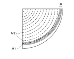
- FIG. 17 is an explanatory view showing the state of the modified layer formed inside the processed wafer W by the first eccentricity correction method.
- the unbonded region Ae is formed eccentrically with respect to the processed wafer W in step A1.
- the peripheral modification layer M1 is formed in a ring shape concentric with the bonding region Ac (unbonded region Ae) in step A2. Therefore, in step A3, the internal surface modification layer M2 is formed along the peripheral modification layer M1, that is, in a spiral shape concentric with the bonding region Ac and the peripheral modification layer M1.
- both the peripheral modification layer M1 and the internal surface modification layer M2 are formed while the eccentricity correction is performed.
- the internal surface modification layer M2 is formed concentrically with the peripheral modification layer M1 formed following the eccentricity of the junction region Ac, thereby modifying the internal surface. It is possible to prevent the layer M2 from being formed radially inside the peripheral modification layer M1.
- the internal surface modification layer M2 is formed following the eccentricity.
- the eccentricity correction operation is internal. There is a concern that the formation operation of the surface modification layer M2 cannot be followed, resonance and a decrease in guide life. Therefore, in the following second eccentricity correction method, the eccentricity correction operation is not performed at least in the central portion of the processed wafer W.
- FIG. 18 is an explanatory view showing the state of the modified layer formed inside the processed wafer W by the second eccentricity correction method.
- the unbonded region Ae is formed eccentrically with respect to the processed wafer W in step A1.
- the peripheral modification layer M1 is formed in a ring shape concentric with the bonding region Ac (unbonded region Ae) in step A2.
- a buffer layer B is formed as an internal surface modification layer of the above. Specifically, after the rotation of the chuck 100 starts, the rotation speed is rate-determined (constant speed), and then the chuck 100 (processed wafer W) is rotated at least once (360 degrees) as shown in FIG.
- the laser head 110 periodically irradiates the inside of the processed wafer W with the laser beam L to form the annular internal surface modification layer M2.
- FIG. 1 An internal surface modification layer M2 as a buffer layer B concentric with the bonding region Ac and the peripheral modification layer M1 as shown in FIG. 19 is formed.
- the buffer layer B is formed, for example, with a processing width (for example, 500 ⁇ m) equal to or larger than the eccentric amount of the bonding region Ac.
- the radial spacing Q of the internal surface modification layer M2 in the buffer layer B can be arbitrarily set.
- the internal surface modification layer M2 as the second internal surface modification layer is spirally formed, for example, from between the processing widths of the buffer layer B.
- the above-mentioned eccentricity correction is not performed.
- the concentric internal surface modification layer M2 constituting the peripheral modification layer M1 and the buffer layer B is formed while performing eccentric correction, and is radially inside the buffer layer B. Eccentricity correction is not performed in the formation of the spiral internal surface modification layer M2 formed in.
- the buffer layer B formed with a processing width equal to or larger than the eccentricity of the junction region Ac is formed inside the peripheral modification layer M1 in the radial direction to form a spiral inside. It is not necessary to perform eccentricity correction in the formation of the surface modification layer M2. That is, even if the inner surface modification layer M2 is formed eccentrically, the amount of eccentricity is absorbed in the processing width of the buffer layer B, so that the inner surface modification layer M2 reaches the radial outside of the peripheral modification layer M1. None. Further, since it is not necessary to perform eccentricity correction when forming the inner surface modified layer M2, the inner surface modified layer M2 can be formed more easily.
- FIG. 20 is an explanatory diagram showing the state of the modified layer formed inside the processed wafer W by the third eccentricity correction method.
- the unbonded region Ae is formed eccentrically with respect to the processed wafer W in step A1.
- the peripheral modification layer M1 is formed in a ring shape concentric with the bonding region Ac (unbonded region Ae) in step A2.
- the laser head 110 is the processing wafer W on the radial inside of the peripheral modification layer M1 formed in a concentric annular shape with the bonding region Ac (unbonded region Ae) in step A2.
- Eccentricity correction is performed in the range located on the outer peripheral portion of. That is, while moving the laser head 110 from the outside in the radial direction to the inside, the rotation mechanism 103 rotates the chuck 100 so that the center of the chuck 100 and the center of the bonding region Ac coincide with each other, and the movement mechanism 104 moves the chuck 100. Move in the Y-axis direction.
- the formation range of the internal surface modification layer M2 on the processed wafer W is divided into a plurality of regions along the radial direction, and the eccentric stroke is gradually shortened according to such regions.
- the formation range of the internal surface modification layer M2 is divided into a central region R11 and four annular regions R12 to R15, and the amount of eccentricity of 100 ⁇ m is corrected by 20 ⁇ m in each annular region R12 to R15.
- the case, that is, the case where the eccentric stroke is attenuated by 20 ⁇ m is illustrated.
- the eccentricity correction is performed in the range located on the outer peripheral portion of the processed wafer W (annular regions R12 to R15 in FIG. 20), thereby performing the eccentricity correction in the vicinity of the central portion.
- the above-mentioned eccentricity correction (attenuation of the eccentric stroke) is completed at the outer peripheral portion of the processed wafer W, the eccentricity amount is 0 ⁇ m, and the central portion (center region R11 in FIG. The centers of the regions Ac are aligned.
- the inner surface modification layer M2 is formed in this way, the rotation speed of the chuck 100 is slow when the laser head 110 is located on the outer peripheral portion, so that eccentricity correction can be appropriately performed.
- the amount of eccentricity can be absorbed to form the inner surface modified layer M2 inside the peripheral modified layer M1.
- the high-speed rotation speed of the chuck 100 can be maintained, and as a result, the circumferential spacing P of the internal surface modification layer M2 can be made constant. ..
- the number of annular regions for performing eccentricity correction is not limited to this example, and can be set arbitrarily. Further, it is not always necessary to gradually correct the eccentricity for each annular region as in this example, and the eccentricity correction may be continuously performed from the outer periphery to the center of the processed wafer W. Further, for example, the eccentricity correction may be performed only while the laser head 110 irradiates the laser beam L from the outside for several rounds.
- the eccentricity correction be completed within half the radius (r / 2) of the processed wafer W.
- the radius of the central region R11 shown in FIG. 20 is preferably r / 2 or more.
- the internal surface modification layer M2 in step A3 is formed as described above. As described above, by performing the eccentricity correction in forming the internal surface modification layer M2, the edge trim treatment and the thinning treatment can be easily performed. Further, for this reason, it becomes easy to maintain the quality of the edge trim treatment and the thinning treatment, and the control in these treatments can be simplified.
- the formation interval of the internal surface modification layer M2 is uniform. Then, in order to control the formation interval to be constant, the rotation speed of the chuck 100 and the frequency of the laser beam L are controlled in the formation of the internal surface modification layer M2 in step A3.
- the circumferential interval P of the internal surface modification layer M2 becomes a critical value at which the interval cannot be further increased. Reach. Then, when the irradiation position of the laser beam L further moves inward in the radial direction in such a state, the circumferential interval P becomes smaller, and the internal surface modification layer M2 overlaps on the same processing line at the center of the processed wafer W. In some cases. Therefore, the central portion of the processed wafer W may not be properly separated.
- the next (second) laser beam L escape light is generated, and a part of the laser beam is transmitted downward. There was a risk of affecting the device layer D.
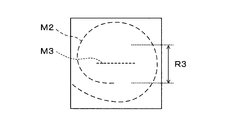
- the present inventors have come up with a method of forming the central modified layer M3 as a method for appropriately separating the central portion of the processed wafer W. That is, the formation of the internal surface modification layer M2 is completed near the center of the processed wafer W where the circumferential interval P reaches the critical value, and as shown in FIG. 21, the center is radially inside the internal surface modification layer M2.
- the modified layer M3 is formed.
- the formation range R3 of the central modified layer M3 shown in FIG. 21 can be obtained from, for example, the lowest value of the frequency of the laser beam L and the highest value of the rotation speed of the chuck 100 (for example, 1 from the center of the processed wafer W). Range of about 2 mm).
- the internal surface modification layer M2 by terminating the formation of the internal surface modification layer M2 at a desired position determined from the rotation speed of the chuck 100 and the frequency of the laser light, it is appropriate to suppress the overlap formation of the internal surface modification layer M2.
- the processed wafer W can be separated, and the generation of missing light of the laser beam L can be suppressed.
- the cracks C2 that self-promote from the internal surface modified layer M2 are connected to each other at the central portion of the processed wafer W and are convex. It is possible to suppress the formation of the portion.
- the central modified layer M3 can be formed in any shape inside the inner surface modified layer M2 in the radial direction.
- the central modified layer M3 is formed by a plurality of straight lines, and according to the illustrated example, seven straight lines, but the shape of the central modified layer M3 is not limited to this.
- the central modified layer M3 may be formed by less than seven lines, for example, only one straight line as shown in FIG. 22, as long as the central portion of the processed wafer W can be properly separated. By reducing the number of formed central modified layers M3 in this way, the tact required to form the central modified layer M3 can be reduced.
- the central modified layer M3 is not limited to a linear shape, and may be formed only in a curved shape, or may be formed by combining a curved shape and a linear shape, for example.
- a plurality of central modified layers M3 may be formed so as to overlap each other, or laser light may escape at the intersection. There is a risk. Further, when the central modified layers M3 are formed close to each other, the cracks C3 extending from the central modified layer M3 are connected to each other, whereby a convex portion is formed in the central portion of the processed wafer W, and the processed wafer W is formed. There is a risk that the flatness of the separation surface will deteriorate.
- the processing lines of the central modified layer M3 are formed independently without crossing each other and close to each other, and the cracks C3 extending in the plane direction from the adjacent central modified layer M3 are not connected to each other. Is desirable. In such a case, it is desirable that the formation interval of the central modified layer M3 is, for example, 10 ⁇ m or more.
- the central modified layer M3 in step A4 is formed as described above.
- the spiral internal surface modification layer M2 can be appropriately formed. That is, even when the inner surface modified layer M2 is formed eccentrically with respect to the processed wafer W, the eccentric amount can be absorbed by the buffer layer B, so that the inner surface modified layer M2 is peripherally modified. It is not formed so as to overlap with the layer M1. As a result, the quality of the edge trimming process can be maintained.
- the present embodiment it is not necessary to perform eccentricity correction in forming the central portion of the processed wafer W, that is, the spiral internal surface modification layer M2.
- the control for forming the inner surface modified layer M2 can be simplified, and the inner surface modified layer M2 can be easily formed.
- it is possible to appropriately reduce the above-mentioned concerns such as the occurrence of resonance and the decrease in guide life.
- the spiral internal surface modification layer M2 is formed from the processing width of the buffer layer B.
- the position where the formation of the spiral internal surface modification layer M2 starts can be arbitrarily determined.
- the internal surface modification layer M2 is peripherally modified. It is possible to reduce the influence on the separation of the processed wafer W while avoiding the formation on the radial outer side of the layer M1. Specifically, since the unformed region of the internal surface modification layer M2 can be reduced, the processed wafer W can be appropriately separated.
- the internal surface modified layer M2 is formed in the plane of the processed wafer W so as to be spirally drawn in one stroke, the tact involved in the formation of the internal surface modified layer M2 is improved. be able to.
- the internal surface modification layer M2 is formed so that the circumferential spacing P and the radial spacing Q are uniform in the plane of the processed wafer W, respectively.
- the formation interval of the internal surface modification layer M2 is not limited to this.
- FIG. 23 is an explanatory view showing a method of forming the internal surface modification layer M2 according to the second embodiment.
- areas having different radial intervals Q of the internal surface modification layer M2 are formed in the surface of the processed wafer W on which the internal surface modification layer M2 according to the second embodiment is formed. ing. Specifically, a wide spacing region R1 in which the radial spacing Q of the internal surface modifying layer M2 is widely formed on the radial outer side of the processed wafer W, and an internal surface modifying layer M2 on the radial inner side of the wide spacing region R1. A narrow spacing region R2 is formed in which the radial spacing Q is narrowly formed.
- the circumferential spacing P of the internal surface modification layer M2 is constant over the entire circumference together with the wide spacing region R1 and the narrow spacing region R2.
- the inner surface modified layer M2 formed in the wide interval region R1 is the outer peripheral side modified layer M2e
- the inner surface modified layer M2 formed in the narrow interval region R2 is the inner peripheral side modified layer M2c. In some cases.
- the outer peripheral side modified layer M2e is prevented from connecting the cracks C2 extending in the plane direction when the adjacent outer peripheral side modified layer M2e is formed.
- Formation interval Q1 is set.
- the outer peripheral side modified layer M2e is formed, for example, from the processing width of the buffer layer B, and is formed inside the buffer layer B in the radial direction.
- the inner peripheral side modified layer M2c is connected so that the cracks C2 extending in the plane direction when the adjacent inner peripheral side modified layer M2c is formed are connected to each other.
- Formation interval Q2 is set.
- the formation interval Q1 of the outer peripheral side modified layer M2e can be 60 ⁇ m
- the formation interval Q2 of the inner peripheral side modified layer M2c can be 10 ⁇ m.
- the internal surface modification layer M2 is formed by irradiating the inside of the processed wafer W with a laser beam to amorphize (polycrystallize) the irradiated portion of the laser beam.
- compressive stress is generated in the internal surface modification layer M2 as shown in FIG. 24 (a).
- the cracks C1 of the adjacent outer peripheral side modified layer M2e are not connected in the wide interval region R1, the generated compressive stress is accumulated in the outer peripheral side modified layer M2e.
- FIG. 24A tensile stress due to compressive stress is accumulated between the outer peripheral side modified layers M2e adjacent to each other in the radial direction.
- the region on which the tensile stress acts (hereinafter, referred to as “tensile region U”) is formed in an annular shape over the entire circumference of the processed wafer W as shown in FIG. 24 (b).
- FIG. 25 is a flow chart showing the main steps of the method of forming the internal surface modification layer M2 and the method of separating the processed wafer W in step A3.
- FIG. 26 is an explanatory diagram schematically showing the main steps of the method of forming the internal surface modification layer M2 and the method of separating the processed wafer W in step A3. Note that FIG. 26 shows a cross-sectional view in the thickness direction of the processed wafer W in the radial half. Further, in FIG. 26, the support wafer S is not shown in order to avoid the complexity of the drawing.
- the peripheral modified layer M1 and the crack C1 are formed on the processed wafer W prior to the formation of the internal surface modified layer M2 (steps A2 in FIGS. 6 and 25). Further, an internal surface modification layer M2 is formed as the buffer layer B.
- the method of forming the buffer layer B is the same as that of the above embodiment.
- a wide interval region R1 is first formed (step A3-1 in FIG. 25).
- the wide interval region R1 rotates the chuck 100 (processed wafer W) and moves the laser head 110 from the radial outside of the processed wafer W toward the inside in the Y-axis direction, thereby causing the processed wafer W to be radially outside. It is formed sequentially from the to the inside in the radial direction.
- the formation interval Q1 of the outer peripheral side modified layer M2e is, for example, 60 ⁇ m.
- the cracks C2 extending from the adjacent outer peripheral side modified layers M2e in the wide interval region R1 are not connected to each other.
- the outer peripheral side modified layer M2e is formed, for example, from the processing width of the buffer layer B.
- the narrow-spaced region R2 is formed as shown in FIG. 26 (b) (step A3-2 in FIG. 25).
- the narrow interval region R2 has a diameter from the center of the processing wafer W by rotating the chuck 100 (processing wafer W) and moving the laser head 110 from the inside to the outside in the radial direction of the processing wafer W in the Y-axis direction. It is formed sequentially toward the outside in the direction.
- the formation interval Q2 of the inner peripheral side modified layer M2c is, for example, 10 ⁇ m.
- the cracks C2 extending from the adjacent inner peripheral side modified layer M2c in the narrow interval region R2 are sequentially connected.
- the crack C2 of the inner peripheral side modified layer M2c located on the outermost peripheral side of the narrow interval region R2 is wide. It is not connected to the crack C2 of the outer peripheral side modified layer M2e located on the innermost peripheral side of the interval region R1.
- the inner peripheral side modified layer M2c is not formed in the central portion of the processed wafer W where the circumferential interval P cannot be maintained.
- a starting point modification layer M2s serving as a starting point for starting the separation of the processed wafer W is formed.
- the internal surface modification layer M2 as the starting point modification layer M2s is formed between the wide interval region R1 and the narrow interval region R2.
- the crack C2 in the wide interval region R1 and the crack C2 in the narrow interval region R2 were connected, and thereby accumulated in the outer peripheral side modified layer M2e of one of the wide interval regions R1.
- the compressive stress is released.
- the one outer peripheral side modified layer M2e is in a state of swelling in the direction in which the first separation wafer W1 and the second separation wafer W2 are separated as shown in FIG. 26D.
- the first separation wafer W1 and the second separation wafer W2 are separated from each other with the crack C2 as a boundary (step A3- in FIG. 25). 4).
- the peeling causes the processing wafer W to be in the thickness direction (peeling direction). Due to the influence of the acting force, the crack C2 propagates radially outward as shown in FIG. 26 (d). Then, it is connected to the crack C2 extending from the adjacent next outer peripheral side modified layer M2e (step A3-5 in FIG. 25).
- the thickness direction (peeling direction) of the processed wafer W is due to such peeling. Due to the influence of the force acting on the crack C2, the crack C2 further propagates outward in the radial direction.
- step A3 the formation process of the internal surface modification layer M2 in step A3 is completed, and then the inner peripheral side
- the central modified layer M3 is formed radially inside the modified layer M2c (step A4 in FIGS. 6 and 25), and then the peripheral edge We and the second separation wafer W2 are removed (FIGS. 6 and 25). Step A5).
- the internal surface modification layer M2 is formed on the processed wafer W, and the internal surface modification layer M2 has a wide interval region R1 and a narrow interval region R2. Then, in the wide interval region R1, the peeling of the first separation wafer W1 and the second separation wafer W2 proceeds in a chain reaction as described above.
- the peeling of the first separation wafer W1 and the second separation wafer W2 causes a gap in the processing wafer W in the thickness direction. That is, as shown in FIG. 26 (e), a region in which the first separation wafer W1 and the second separation wafer W2 are not connected is formed in the plane of the processing wafer W, so that the second separation wafer later is formed. The force required for the peeling process of W2 is reduced.
- the number of formed internal surface modified layers M2 can be reduced by increasing the radial interval Q of the internal surface modified layer M2 in the wide interval region R1, so that the internal surface modified layer M2 can be modified.
- the time required for the formation of the layer M2 can be reduced, and the throughput can be improved.
- the first separation wafer W1 and the second separation wafer W2 in the wide interval region R1 use the crack C2 that spontaneously propagates by releasing the accumulated stress as a base point. Be separated. Therefore, especially in the wide interval region R1, a smooth separation surface having a periodic structure can be obtained.
- FIG. 27 shows the processing wafers in (a) when the radial spacing Q of the processing wafer W is constant in the plane of the processing wafer W and (b) when the wide spacing region R1 and the narrow spacing region R2 are formed. It is a photograph which imaged the separation surface of W. As shown in FIG. 27, by forming the wide-interval region R1 and the narrow-interval region R2 and spontaneously advancing the crack C2 by releasing the accumulated stress, the surface roughness after separation is improved and smooth. A good separation surface can be obtained.
- the buffer layer B is formed, and the spiral inner surface modification layer M2 (outer peripheral side modification layer M2e and inner peripheral side modification layer M2e) is formed between the processing widths of the buffer layer B. M2c) is formed.
- the wide interval region R1 is formed on the outer side in the radial direction and the narrow interval region R2 is formed on the inner side in the radial direction.
- the processing wafer W in the plan view A narrow space region R2 may be formed on the outer side in the radial direction, and a wide space region R1 may be formed on the inner side of the narrow space region R2.
- wide-spaced regions R1 and narrow-spaced regions R2 may be alternately formed on the radial outer side of the processed wafer W.
- the wide spacing region R1 and the narrow spacing region R2 are formed with respect to the radial direction of the processed wafer W, that is, the radial spacing Q of the internal surface modification layer M2 is changed.
- the circumferential interval P pulse pitch
- both the radial interval Q and the circumferential interval P may be changed. In such a case, the number of internal surface modification layers M2 formed in the plane of the processed wafer W is further reduced, so that the throughput can be further improved.
- the processing wafer W is started to be separated by forming the starting point modifying layer M2s between the wide interval region R1 and the narrow interval region R2, but the separation of the processing wafer W is started.
- the method of is not limited to this.
- a wide interval region R1 is formed from the radial outer side to the inner side of the processed wafer W to a predetermined arbitrary position, and then processed as shown in FIG. 29 (b). Separation may be started by forming a narrow interval region R2 from the center of the wafer W toward the outer side in the radial direction and merging with the internal surface modification layer M2 of the wide interval region R1.
- Control device 110 Laser head L Laser light B Buffer layer M1 Peripheral reformer M2 Internal surface reformer W processing wafer
Abstract
Description
変形例1として、ステップA2の周縁改質層M1の形成とステップA3の内部面改質層M2の形成の順序を入れ替えてもよい。かかる場合、ウェハ処理は、ステップA1、ステップA3、ステップA2、ステップA4~A8の順で行われる。
変形例2として、ステップA4の中心改質層M3の形成は、ステップA2の周縁改質層M1の形成前に行われてもよい。かかる場合、ウェハ処理は、ステップA1、ステップA4、ステップA2~A3、ステップA5~A8の順で行われる。
変形例3として、ステップA4の中心改質層M3の形成は、ステップA3の内部面改質層M2の形成前に行われてもよい。かかる場合、ウェハ処理は、ステップA1~A2、ステップA4、ステップA3、ステップA5~A8の順で行われる。
変形例4として、ステップA1の未接合領域Aeの形成は、ステップA2の周縁改質層M1の形成後に行われてもよい。かかる場合、ウェハ処理は、ステップA2、ステップA1、ステップA3~A8の順で行われる。
変形例5として、ステップA1の未接合領域Aeの形成は、ステップA3の内部面改質層M2の形成後に行われてもよい。かかる場合、ウェハ処理は、ステップA2~A3、ステップA1、ステップA4~A8の順で行われる。
省略例1として、ステップA6の周縁改質層M1、内部面改質層M2及び中心改質層M3の除去は、ステップA8におけるウェットエッチングにより行われてもよい。かかる場合、ステップA6の研削処理を省略することができる。
省略例2として、ステップA6の研削処理において周縁改質層M1、内部面改質層M2及び中心改質層M3が適切に除去され、また研削痕が形成されていない場合、ステップA8のウェットエッチングを省略することができる。
省略例3として、ウェハ処理システム1に対して、未接合領域Aeが形成された重合ウェハTが搬入される場合、ステップA1の未接合領域Aeの形成を省略することができる。
90 制御装置
110 レーザヘッド
L レーザ光
B バッファ層
M1 周縁改質層
M2 内部面改質層
W 処理ウェハ
Claims (8)
- 処理対象体を処理する処理装置であって、
前記処理対象体の内部にレーザ光を照射して、面方向に沿って複数の改質層を形成する改質部と、
少なくとも前記改質部の動作を制御する制御部と、を備え、
前記制御部は、
前記処理対象体の除去対象の周縁部の剥離の基点となる周縁改質層と、
前記周縁改質層の径方向内側において、前記周縁改質層と同心円の環状に形成される第1の内部面改質層と、
前記第1の内部面改質層の径方向内側において、螺旋状に形成される第2の内部面改質層と、を形成するように前記改質部を制御する、処理装置。 - 前記制御部は、前記第1の内部面改質層の径方向における加工幅が、前記処理対象体の中心と当該処理対象体を保持する保持部の中心との偏心量よりも大きく形成されるように、前記改質部を制御する、請求項1に記載の処理装置。
- 前記制御部は、前記第1の内部面改質層の径方向における加工幅の間から、前記第2の内部面改質層の形成を開始するように前記改質部を制御する、請求項1または2に記載の処理装置。
- 処理対象体を処理する処理方法であって、
改質部により、保持部に保持された前記処理対象体の内部にレーザ光を照射して、面方向に沿って複数の改質層を形成し、
前記処理対象体の除去対象の周縁部の剥離の基点となる周縁改質層を形成することと、
前記周縁改質層の径方向内側において、前記周縁改質層と同心円の環状に形成される第1の内部面改質層を形成することと、
前記第1の内部面改質層の径方向内側において、螺旋状に形成される第2の内部面改質層を形成することと、を含む、処理方法。 - 前記第1の内部面改質層の形成にあたり、
前記改質部に対して保持部に保持された前記処理対象体を相対的に回転させながら、前記改質部から処理対象体の内部に前記レーザ光を周期的に照射して、前記周縁改質層と同心円状の第1の内部面改質層を形成し、
その後、前記保持部に対して前記改質部を相対的に径方向に移動させ、
前記周縁改質層と同心円状の前記第1の内部面改質層の形成と前記改質部の径方向への移動とを繰り返し行って、面方向に環状の前記第1の内部面改質層を形成する、請求項4に記載の処理方法。 - 記第1の内部面改質層は、径方向において前記保持部の中心と前記処理対象体の中心との偏心量よりも大きい加工幅で形成される、請求項4または5に記載の処理方法。
- 前記第2の内部面改質層は、前記第1の内部面改質層の径方向における加工幅の間から形成が開始される、請求項6に記載の処理方法。
- 前記第2の内部面改質層の形成にあたり、
保持部に保持された前記処理対象体を相対的に回転させながら、前記改質部から処理対象体の内部に前記レーザ光を周期的に照射し、さらに前記保持部に対して前記改質部を相対的に径方向に移動させて、面方向に螺旋状の前記第2の内部面改質層を形成する、請求項4~7のいずれか一項に記載の処理方法。
Priority Applications (4)
| Application Number | Priority Date | Filing Date | Title |
|---|---|---|---|
| CN202080050532.XA CN114096375B (zh) | 2019-07-18 | 2020-07-09 | 处理装置和处理方法 |
| US17/627,706 US20220254638A1 (en) | 2019-07-18 | 2020-07-09 | Processing apparatus and processing method |
| JP2021533020A JP7170880B2 (ja) | 2019-07-18 | 2020-07-09 | 処理装置及び処理方法 |
| KR1020227004880A KR20220035441A (ko) | 2019-07-18 | 2020-07-09 | 처리 장치 및 처리 방법 |
Applications Claiming Priority (2)
| Application Number | Priority Date | Filing Date | Title |
|---|---|---|---|
| JP2019133070 | 2019-07-18 | ||
| JP2019-133070 | 2019-07-18 |
Publications (1)
| Publication Number | Publication Date |
|---|---|
| WO2021010287A1 true WO2021010287A1 (ja) | 2021-01-21 |
Family
ID=74210801
Family Applications (1)
| Application Number | Title | Priority Date | Filing Date |
|---|---|---|---|
| PCT/JP2020/026891 WO2021010287A1 (ja) | 2019-07-18 | 2020-07-09 | 処理装置及び処理方法 |
Country Status (6)
| Country | Link |
|---|---|
| US (1) | US20220254638A1 (ja) |
| JP (1) | JP7170880B2 (ja) |
| KR (1) | KR20220035441A (ja) |
| CN (1) | CN114096375B (ja) |
| TW (1) | TW202107553A (ja) |
| WO (1) | WO2021010287A1 (ja) |
Cited By (1)
| Publication number | Priority date | Publication date | Assignee | Title |
|---|---|---|---|---|
| WO2023021952A1 (ja) * | 2021-08-16 | 2023-02-23 | 東京エレクトロン株式会社 | 処理方法及び処理システム |
Citations (3)
| Publication number | Priority date | Publication date | Assignee | Title |
|---|---|---|---|---|
| JP2006108532A (ja) * | 2004-10-08 | 2006-04-20 | Disco Abrasive Syst Ltd | ウエーハの研削方法 |
| JP2016215231A (ja) * | 2015-05-19 | 2016-12-22 | パナソニックIpマネジメント株式会社 | 脆性基板のスライス装置及び方法 |
| JP2018043340A (ja) * | 2016-09-15 | 2018-03-22 | 株式会社荏原製作所 | 基板加工方法および基板加工装置 |
Family Cites Families (11)
| Publication number | Priority date | Publication date | Assignee | Title |
|---|---|---|---|---|
| JP4110219B2 (ja) * | 2002-08-30 | 2008-07-02 | 株式会社東京精密 | レーザーダイシング装置 |
| JP4776994B2 (ja) * | 2005-07-04 | 2011-09-21 | 浜松ホトニクス株式会社 | 加工対象物切断方法 |
| EP2544220A4 (en) * | 2010-03-05 | 2015-12-02 | Namiki Precision Jewel Co Ltd | SEMICONDUCTOR SUBSTRATE, PRODUCTION METHOD FOR THE SINGLE CRYSTAL SUBSTRATE, PRODUCTION PROCESS FOR A SINGLE CRYSTAL SUBSTRATE WITH A MULTILAYER FILM AND DEVICE MANUFACTURING METHOD |
| JP2012109341A (ja) * | 2010-11-16 | 2012-06-07 | Shibuya Kogyo Co Ltd | 半導体材料の切断方法と切断装置 |
| JP6044919B2 (ja) | 2012-02-01 | 2016-12-14 | 信越ポリマー株式会社 | 基板加工方法 |
| JP6482425B2 (ja) * | 2015-07-21 | 2019-03-13 | 株式会社ディスコ | ウエーハの薄化方法 |
| JP6523882B2 (ja) * | 2015-09-02 | 2019-06-05 | 株式会社ディスコ | ウエーハの加工方法 |
| JP6504977B2 (ja) * | 2015-09-16 | 2019-04-24 | 株式会社ディスコ | ウエーハの加工方法 |
| JP2017071074A (ja) * | 2015-10-05 | 2017-04-13 | 国立大学法人埼玉大学 | 内部加工層形成単結晶基板の製造方法、および、単結晶基板の製造方法 |
| JP6541605B2 (ja) * | 2016-03-30 | 2019-07-10 | 東京エレクトロン株式会社 | 基板処理装置、及び基板処理装置の撮像方法 |
| JP6918420B2 (ja) * | 2017-09-14 | 2021-08-11 | 株式会社ディスコ | ウェーハの加工方法 |
-
2020
- 2020-07-06 TW TW109122695A patent/TW202107553A/zh unknown
- 2020-07-09 CN CN202080050532.XA patent/CN114096375B/zh active Active
- 2020-07-09 US US17/627,706 patent/US20220254638A1/en active Pending
- 2020-07-09 KR KR1020227004880A patent/KR20220035441A/ko unknown
- 2020-07-09 WO PCT/JP2020/026891 patent/WO2021010287A1/ja active Application Filing
- 2020-07-09 JP JP2021533020A patent/JP7170880B2/ja active Active
Patent Citations (3)
| Publication number | Priority date | Publication date | Assignee | Title |
|---|---|---|---|---|
| JP2006108532A (ja) * | 2004-10-08 | 2006-04-20 | Disco Abrasive Syst Ltd | ウエーハの研削方法 |
| JP2016215231A (ja) * | 2015-05-19 | 2016-12-22 | パナソニックIpマネジメント株式会社 | 脆性基板のスライス装置及び方法 |
| JP2018043340A (ja) * | 2016-09-15 | 2018-03-22 | 株式会社荏原製作所 | 基板加工方法および基板加工装置 |
Cited By (1)
| Publication number | Priority date | Publication date | Assignee | Title |
|---|---|---|---|---|
| WO2023021952A1 (ja) * | 2021-08-16 | 2023-02-23 | 東京エレクトロン株式会社 | 処理方法及び処理システム |
Also Published As
| Publication number | Publication date |
|---|---|
| KR20220035441A (ko) | 2022-03-22 |
| JP7170880B2 (ja) | 2022-11-14 |
| CN114096375A (zh) | 2022-02-25 |
| CN114096375B (zh) | 2024-01-09 |
| TW202107553A (zh) | 2021-02-16 |
| JPWO2021010287A1 (ja) | 2021-01-21 |
| US20220254638A1 (en) | 2022-08-11 |
Similar Documents
| Publication | Publication Date | Title |
|---|---|---|
| JP7058320B2 (ja) | 基板処理システム、基板処理方法及びコンピュータ記憶媒体 | |
| JP6934563B2 (ja) | 基板処理システム及び基板処理方法 | |
| JPWO2019208359A1 (ja) | 基板処理システム及び基板処理方法 | |
| WO2020213479A1 (ja) | 処理装置及び処理方法 | |
| WO2020213478A1 (ja) | 処理装置及び処理方法 | |
| JPWO2020129730A1 (ja) | 基板処理装置及び基板処理方法 | |
| WO2021010287A1 (ja) | 処理装置及び処理方法 | |
| WO2021010286A1 (ja) | 処理装置及び処理方法 | |
| JP2021019056A (ja) | 処理装置及び処理方法 | |
| WO2021010284A1 (ja) | 処理装置及び処理方法 | |
| WO2021010285A1 (ja) | 処理装置及び処理方法 | |
| JP7086201B2 (ja) | 基板処理システム及び基板処理方法 | |
| WO2020195567A1 (ja) | 処理装置及び処理方法 | |
| JPWO2020129734A1 (ja) | 基板処理装置及び基板処理方法 |
Legal Events
| Date | Code | Title | Description |
|---|---|---|---|
| 121 | Ep: the epo has been informed by wipo that ep was designated in this application |
Ref document number: 20839984 Country of ref document: EP Kind code of ref document: A1 |
|
| ENP | Entry into the national phase |
Ref document number: 2021533020 Country of ref document: JP Kind code of ref document: A |
|
| NENP | Non-entry into the national phase |
Ref country code: DE |
|
| ENP | Entry into the national phase |
Ref document number: 20227004880 Country of ref document: KR Kind code of ref document: A |
|
| 122 | Ep: pct application non-entry in european phase |
Ref document number: 20839984 Country of ref document: EP Kind code of ref document: A1 |