WO2023008227A1 - プローブカード - Google Patents
プローブカード Download PDFInfo
- Publication number
- WO2023008227A1 WO2023008227A1 PCT/JP2022/027830 JP2022027830W WO2023008227A1 WO 2023008227 A1 WO2023008227 A1 WO 2023008227A1 JP 2022027830 W JP2022027830 W JP 2022027830W WO 2023008227 A1 WO2023008227 A1 WO 2023008227A1
- Authority
- WO
- WIPO (PCT)
- Prior art keywords
- conductor
- transmission conductor
- transmission
- conductors
- probe
- Prior art date
- Legal status (The legal status is an assumption and is not a legal conclusion. Google has not performed a legal analysis and makes no representation as to the accuracy of the status listed.)
- Ceased
Links
Images


Classifications
-
- G—PHYSICS
- G01—MEASURING; TESTING
- G01R—MEASURING ELECTRIC VARIABLES; MEASURING MAGNETIC VARIABLES
- G01R1/00—Details of instruments or arrangements of the types included in groups G01R5/00 - G01R13/00 and G01R31/00
- G01R1/02—General constructional details
- G01R1/06—Measuring leads; Measuring probes
- G01R1/067—Measuring probes
- G01R1/073—Multiple probes
- G01R1/07307—Multiple probes with individual probe elements, e.g. needles, cantilever beams or bump contacts, fixed in relation to each other, e.g. bed of nails fixture or probe card
- G01R1/07314—Multiple probes with individual probe elements, e.g. needles, cantilever beams or bump contacts, fixed in relation to each other, e.g. bed of nails fixture or probe card the body of the probe being perpendicular to test object, e.g. bed of nails or probe with bump contacts on a rigid support
-
- G—PHYSICS
- G01—MEASURING; TESTING
- G01R—MEASURING ELECTRIC VARIABLES; MEASURING MAGNETIC VARIABLES
- G01R1/00—Details of instruments or arrangements of the types included in groups G01R5/00 - G01R13/00 and G01R31/00
- G01R1/02—General constructional details
- G01R1/06—Measuring leads; Measuring probes
- G01R1/067—Measuring probes
- G01R1/073—Multiple probes
- G01R1/07307—Multiple probes with individual probe elements, e.g. needles, cantilever beams or bump contacts, fixed in relation to each other, e.g. bed of nails fixture or probe card
- G01R1/07342—Multiple probes with individual probe elements, e.g. needles, cantilever beams or bump contacts, fixed in relation to each other, e.g. bed of nails fixture or probe card the body of the probe being at an angle other than perpendicular to test object, e.g. probe card
-
- G—PHYSICS
- G01—MEASURING; TESTING
- G01R—MEASURING ELECTRIC VARIABLES; MEASURING MAGNETIC VARIABLES
- G01R31/00—Arrangements for testing electric properties; Arrangements for locating electric faults; Arrangements for electrical testing characterised by what is being tested not provided for elsewhere
- G01R31/26—Testing of individual semiconductor devices
-
- H—ELECTRICITY
- H10—SEMICONDUCTOR DEVICES; ELECTRIC SOLID-STATE DEVICES NOT OTHERWISE PROVIDED FOR
- H10P—GENERIC PROCESSES OR APPARATUS FOR THE MANUFACTURE OR TREATMENT OF DEVICES COVERED BY CLASS H10
- H10P74/00—Testing or measuring during manufacture or treatment of wafers, substrates or devices
Definitions
- the present invention relates to probe cards.
- Patent Document 1 describes an example of a probe card.
- the probe card has an interposer positioned between the electronic device and the tester.
- a plurality of probes are provided on the lower surface of the interposer to contact a plurality of electrodes provided on the upper surface of the electronic device.
- Inside the interposer a plurality of conductors such as wiring and vias connected to a plurality of probes are provided.
- the electronic device and the tester are electrically connected through probes provided on the lower surface of the interposer and conductors provided inside the interposer.
- Patent Document 2 describes an example of a probe card.
- the probe card has a flexible substrate.
- the electronic device and the tester are electrically connected via conductors such as wiring extending along the surface of the flexible substrate.
- a high frequency signal may be transmitted between the electronic device and the tester via the probe card.
- a probe card including an interposer such as the probe card described in Patent Document 1
- the probes provided on the lower surface of the interposer and the conductors provided inside the interposer are relatively long, and the probes and the conductors are relatively long.
- RF signals transmitted through can be relatively lossy.
- a probe card having a flexible substrate such as the probe card described in Patent Document 2
- DC signals direct current signals
- LF signals The number of signals
- An example of the object of the present invention is to reduce the transmission loss of signals transmitted between the electronic device and the tester while not reducing the number of signals transmitted between the electronic device and the tester.
- Other objects of the present invention will become clear from the description herein.
- One aspect of the present invention is an insulating layer; a first conductor at least partially extending along the surface of the insulating layer; a second conductor, at least a portion of which passes through at least a portion of said insulating layer; is a probe card comprising
- FIG. 4 is a bottom view of the probe card according to Embodiment 1.
- FIG. FIG. 2 is a cross-sectional view taken along the line AA′ of FIG. 1;
- FIG. 5 is a cross-sectional view of a probe card according to Embodiment 2;
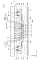
- FIG. 1 is a bottom view of the probe card 10A according to Embodiment 1.
- FIG. FIG. 2 is a cross-sectional view taken along the line AA' of FIG. FIG. 2 shows the electronic device 20 and the tester 30 together with the probe card 10A.
- the direction from the proximal end to the distal end of the arrow is the positive direction of the direction indicated by the arrow. It indicates that the direction from the tip of the arrow to the base is the negative direction of the direction indicated by the arrow.
- a white circle with an X indicating the second direction Y or the third direction Z indicates that the direction from the front to the back of the paper is the positive direction of the direction indicated by the white circle, and the direction from the back to the front of the paper is indicated by the white circle. indicates that it is in the negative direction.
- the first direction X is a direction parallel to the horizontal direction perpendicular to the vertical direction.
- the first direction X is a direction parallel to the longitudinal direction of the rigid substrate 100, which will be described later.
- the positive direction of the first direction X is the direction from the second through hole 104 described later toward the first through hole 102 described later.
- the negative direction of the first direction X is the direction from the first through hole 102 toward the second through hole 104 .
- the second direction Y is a direction parallel to a direction perpendicular to both the vertical direction and the first direction X. As shown in FIG. Specifically, the second direction Y is a direction parallel to the lateral direction of the rigid substrate 100 .
- the positive direction of the second direction Y and the negative direction of the second direction Y are opposite to each other.
- the third direction Z is a direction parallel to the vertical direction. Specifically, the positive direction of the third direction Z is a direction from below to above.
- the negative direction of the third direction Z is a direction from above to below.
- the probe card 10A is positioned between the electronic device 20 and the tester 30 in the third direction Z.
- the electronic device 20 is positioned below the probe card 10A.
- the electronic device 20 is, for example, a wafer.
- the tester 30 is located above the probe card 10A.
- the probe card 10A includes a rigid substrate 100, a probe head 200A, a first interposer 300A, a stiffener 400, a plurality of first coaxial connectors 410, a plurality of second coaxial connectors 420, a plurality of first coaxial cables 430 and a plurality of second coaxial cables.
- a cable 440 is provided.
- the rigid board 100 is, for example, a PCB (Printed Circuit Board).
- the rigid substrate 100 has a thickness in a direction parallel to the third direction Z. As shown in FIG.
- a first through hole 102 and a second through hole 104 aligned in the first direction X are provided in the rigid substrate 100 .
- the first through-hole 102 and the second through-hole 104 penetrate the rigid substrate 100 in the third direction Z.
- the first through-hole 102 is positioned on the positive side in the first direction X with respect to the probe head 200A when viewed from the negative direction in the third direction Z.
- the second through hole 104 is located on the negative side of the first direction X with respect to the probe head 200A when viewed from the negative direction of the third direction Z.
- the rigid board 100 has multiple first connection conductors 110 .
- Each first connection conductor 110 includes a plurality of first vias 112 extending in the third direction Z and first wirings 114 extending in a direction orthogonal to the third direction Z.
- the position of the upper end of the first connection conductor 110 and the position of the lower end of the first connection conductor 110 are shifted in the direction perpendicular to the third direction Z by the first wiring 114 .
- the first wiring 114 extends from the first via 112 including the lower end of each first connection conductor 110 toward the first via 112 including the upper end of each first connection conductor 110 . It extends in a direction away from the center in the first direction X.
- the pitch in the first direction X between the upper ends of the plurality of first connection conductors 110 is larger than the pitch in the first direction X between the lower ends of the plurality of first connection conductors 110 .
- the shape of the first connection conductor 110 is not limited to the example shown in FIG.
- the first connection conductor 110 does not have a first wiring 114 extending in a direction orthogonal to the third direction Z, but has a first via 112 extending in a direction parallel to the third direction Z. good too.
- the position of the upper end of the first connection conductor 110 and the position of the lower end of the first connection conductor 110 are aligned in the third direction Z. As shown in FIG.
- the probe head 200A is positioned below the rigid substrate 100 via the first interposer 300A. As shown in FIG. 1, the probe head 200A is located between the first through hole 102 and the second through hole 104 in the first direction X when viewed from the negative direction of the third direction Z. As shown in FIG.
- the probe head 200A has a plurality of probes 210A and insulating supports 220A.
- the plurality of probes 210A when viewed from the negative direction of the third direction Z, are arranged in a matrix.
- the plurality of probes 210A are arranged in a matrix of 8 columns in the first direction X and 7 rows in the second direction Y when viewed from the negative direction of the third direction Z.
- the layout of the multiple probes 210A is not limited to the example shown in FIG.
- the insulating support 220A supports a plurality of probes 210A. As shown in FIG. 2, the insulating support 220A has a thickness in a direction parallel to the third direction Z. As shown in FIG. The upper surface of the insulating support 220A faces the portion of the lower surface of the rigid substrate 100 located between the first through hole 102 and the second through hole 104 in the first direction X through the first interposer 300A. there is The lower surface of the insulating support 220A faces the upper surface of the electronic device 20. As shown in FIG.
- Each probe 210A is provided to penetrate the insulating support 220A in the third direction Z.
- the upper end of each probe 210A protruding upward from the upper surface of the insulating support 220A and the lower end of each probe 210A protruding downward from the lower surface of the insulating support 220A are, for example, An elastic member such as a spring provided between the upper end and the lower end urges them in the third direction Z in directions away from each other.
- the plurality of probes 210A can be individually inserted into and removed from the insulating support 220A. Therefore, when some of the probes 210A need to be replaced due to a defect such as wear, only the defective probe 210A is replaced without replacing the entire probe head 200A. be able to.
- a flexible substrate such as an FPC (Flexible Printed Circuit) provided with multiple probes
- FPC Flexible Printed Circuit
- the maintenance cost of the probe card 10A can be reduced as compared with such a case.
- the plurality of probes 210A may not be individually insertable/removable with respect to the insulating support 220A.
- the first interposer 300A has a first insulating layer 310A, a plurality of first transmission conductors 322A, a plurality of second transmission conductors 324A and a plurality of third transmission conductors 330A.
- the first insulating layer 310A includes a first base region 312A, a first extension region 314A and a second extension region 316A.
- the first insulating layer 310A is, for example, an insulating laminate. This insulating laminate is, for example, an organic multilayer substrate.
- the first base region 312A has a thickness in a direction parallel to the third direction Z.
- the first base region 312A includes a plurality of insulating layers stacked in the third Z direction.
- the upper surface of the first base region 312A faces a portion of the lower surface of the rigid substrate 100 located between the first through-hole 102 and the second through-hole 104 in the first direction X via a plurality of bumps 350. ing.
- the bottom surface of the first base region 312A faces the top surface of the insulating support 220A.
- the first extending region 314A is drawn outward in the positive direction of the first direction X from the lowermost insulating layer of the first base region 312A.
- the first extending region 314A is formed by processing an insulating laminate such as an organic multilayer substrate so that the portion to be the first extending region 314A is thinner in the third direction Z than the portion to be the first base region 312A. is formed by By making the thickness of the first stretched region 314A in the third direction Z smaller than the thickness of the first base region 312A in the third direction Z, the flexibility of the first stretched region 314A is increased to the flexibility of the first base region 312A. can be higher. Therefore, the shape of the first stretched region 314A can be changed to an appropriate shape. In the example shown in FIG. 2 , the first extension region 314A is bent toward the lower surface of the rigid substrate 100 from the first base region 312A toward the first through hole 102 .
- the second extending region 316A is drawn outward in the negative direction of the first direction X from the lowermost insulating layer of the first base region 312A.
- the second extending region 316A is formed by, for example, processing an insulating laminate such as an organic multilayer substrate so that the portion to be the second extending region 316A is thinner in the third direction Z than the portion to be the first base region 312A. is formed by By making the thickness of the second stretched region 316A in the third direction Z smaller than the thickness of the first base region 312A in the third direction Z, the flexibility of the second stretched region 316A is reduced to the flexibility of the first base region 312A. can be higher. Therefore, the shape of the second stretched region 316A can be changed to an appropriate shape.
- the second extension region 316A is bent toward the lower surface of the rigid substrate 100 from the first base region 312A toward the second through hole 104. In the example shown in FIG.
- the plurality of first transmission conductors 322A and the plurality of second transmission conductors 324A transmit signals of the first frequency.
- the plurality of third transmission conductors 330A transmit at least one of a direct current signal (DC signal) and a signal of a second frequency lower than the first frequency.
- the signal of the first frequency transmitted by the first transmission conductor 322A or the second transmission conductor 324A is, for example, a high frequency signal (RF signal).
- the DC signal transmitted by the third transmission conductor 330A is, for example, power supply potential or ground potential.
- the second frequency signal transmitted by the third transmission conductor 330A is, for example, a low frequency signal (LF signal).
- the plurality of first transmission conductors 322A and the plurality of second transmission conductors 324A transmit RF signals. Further, the following description is based on the assumption that the plurality of third transmission conductors 330A transmit at least one of the DC signal and the LF signal.
- the details of the layout of the plurality of first transmission conductors 322A and the plurality of second transmission conductors 324A when viewed from the negative direction of the third direction Z will be described with reference to FIG. Note that the layout of the plurality of first transmission conductors 322A and the plurality of second transmission conductors 324A when viewed from the negative direction of the third direction Z is not limited to the example shown in FIG.
- Each first transmission conductor 322A extends in the positive first direction X from a region overlapping the probe head 200A in the third direction Z. As shown in FIG. The ends of the first transmission conductors 322A on the negative side in the first direction X are located in the positive direction in the first direction X among the plurality of probes 210A arranged in a matrix in the first direction X and the second direction Y. It is connected to one of the seven probes 210A located in the endmost row.
- the end of the first transmission conductor 322A located in the center in the second direction Y is connected to the probe 210A located in the middle row in the second direction Y in the column. .
- the end portion of the first transmission conductor 322A located on the positive direction side in the second direction Y with respect to the first transmission conductor 322A located in the center in the second direction Y is the center row in the second direction Y in the column. , is connected to the probe 210A shifted by two rows in the positive direction of the second direction Y from the .
- the end portion of the first transmission conductor 322A located on the negative direction side in the second direction Y with respect to the first transmission conductor 322A located in the center in the second direction Y is the center row in the second direction Y in the column. , is connected to the probe 210A shifted by two lines in the negative direction of the second direction Y from the .
- the second extending region 316A is provided with three second transmission conductors 324A arranged symmetrically with the three first transmission conductors 322A with respect to the center of the first base region 312A in the first direction X.
- Each second transmission conductor 324A extends in the third direction Z in the negative direction of the first direction X from a region overlapping the probe head 200A.
- the ends of the second transmission conductors 324A on the positive side in the first direction X are located in the negative direction of the first direction X among the plurality of probes 210A arranged in a matrix in the first direction X and the second direction Y. It is connected to one of the seven probes 210A located in the endmost row.
- the end of the second transmission conductor 324A located in the center in the second direction Y is connected to the probe 210A located in the middle row in the second direction Y in the column.
- the end portion of the second transmission conductor 324A located on the positive direction side in the second direction Y with respect to the second transmission conductor 324A located in the center in the second direction Y is the center row in the second direction Y in the column. , is connected to the probe 210A shifted by two rows in the positive direction of the second direction Y from the .
- the end portion of the second transmission conductor 324A located on the negative direction side in the second direction Y with respect to the second transmission conductor 324A located in the center in the second direction Y is the center row in the second direction Y in the column. , is connected to the probe 210A shifted by two lines in the negative direction of the second direction Y from the .
- the first transmission conductor 322A extends along the surface of the first extension region 314A. Therefore, by deforming the shape of the first extension region 314A into an appropriate shape, the first transmission conductor 322A can be pulled out from the first base region 312A toward an appropriate position along the first extension region 314A.
- at least a portion of the first transmission conductor 322A is provided along the bottom surface of the first extension region 314A. Compare the example shown in FIG. 2 with the case where the first transmission conductor 322A is provided along the top surface of the first extension region 314A. In the example shown in FIG.
- the end of the first transmission conductor 322A on the negative direction side in the first direction X and the probe 210A connected to the end of the first transmission conductor 322A and the distance in the third direction Z can be shortened. Therefore, in the example shown in FIG. 2, compared to the case described above, the above-described end of the first transmission conductor 322A and the upper end of the probe 210A connected to the end of the first transmission conductor 322A are It is possible to reduce the transmission loss of the RF signal transmitted between.
- the first transmission conductor 322A may be provided along the upper surface of the first extension region 314A.
- the second transmission conductor 324A extends along the surface of the second extension region 316A. Therefore, by deforming the shape of the second extension region 316A to an appropriate shape, the second transmission conductor 324A can be pulled out from the first base region 312A toward an appropriate position along the second extension region 316A.
- at least a portion of the second transmission conductor 324A is provided along the bottom surface of the second extension region 316A. Compare the example shown in FIG. 2 with the case where the second transmission conductor 324A is provided along the top surface of the second extension region 316A. In the example shown in FIG.
- the end of the second transmission conductor 324A on the positive direction side in the first direction X and the probe 210A connected to the end of the second transmission conductor 324A and the distance in the third direction Z can be shortened. Therefore, in the example shown in FIG. 2, compared to the case described above, the above-described end of the second transmission conductor 324A and the upper end of the probe 210A connected to the end of the second transmission conductor 324A are It is possible to reduce the transmission loss of the RF signal transmitted between.
- the second transmission conductor 324A may be provided along the upper surface of the second extension region 316A.
- each third transmission conductor 330A penetrates in the third direction Z through at least a portion of the first base region 312A.
- each third transmission conductor 330A includes a plurality of second vias 332A extending in a direction parallel to the third direction Z and a second wiring 334A extending in a direction orthogonal to the third direction Z. contains. The position of the upper end of the third transmission conductor 330A and the position of the lower end of the third transmission conductor 330A are shifted in the direction perpendicular to the third direction Z by the second wiring 334A.
- the second trace 334A extends from the second via 332A including the lower end of each third transmission conductor 330A to the second via 332A including the upper end of each third transmission conductor 330A. It extends away from the center of the first direction X of 312A. Accordingly, the pitch in the first direction X between the upper ends of the plurality of third transmission conductors 330A is larger than the pitch in the first direction X between the lower ends of the plurality of third transmission conductors 330A.
- the shape of the third transmission conductor 330A is not limited to the example shown in FIG.
- the plurality of first connection conductors 110 are electrically connected to a plurality of probes 210A different from the probes 210A connected to the first transmission conductor 322A or the second transmission conductor 324A via the plurality of bumps 350 and the plurality of third transmission conductors 330A. properly connected.
- the six first connection conductors 110 are connected to eight bumps 350 via six bumps 350 at the center in the first direction X among the eight bumps 350 and six third transmission conductors 330A. It is electrically connected to the central six probes 210A in the first direction X out of the four probes 210A.
- each third transmission conductor 330A is electrically connected to the lower end of each first connection conductor 110 via each bump 350 .
- the lower end of each third transmission conductor 330A is electrically connected to the upper end of each probe 210A. Therefore, the first interposer 300A makes the pitch of the lower ends of the plurality of first connection conductors 110 in the direction perpendicular to the third direction Z larger than the pitch of the upper ends of the plurality of probes 210A in the direction perpendicular to the third direction Z. ing.
- the structure of the first interposer 300A is not limited to the structure according to this embodiment.
- the first extension region 314A is drawn from the lowest insulating layer of the first base region 312A.
- This embodiment will be compared with the case where the first extension region 314A is led out from an insulating layer above the lowermost insulating layer of the first base region 312A.
- the end of the first transmission conductor 322A on the negative direction side in the first direction X and the upper end of the probe 210A connected to the end of the first transmission conductor 322A can be shortened in the third direction Z.
- the end of the first transmission conductor 322A on the negative direction side in the first direction X and the probe 210A connected to the end of the first transmission conductor 322A can reduce the transmission loss of the RF signal transmitted between the upper end of the
- the first extension region 314A may be drawn from an insulating layer above the lowest insulating layer of the first base region 312A. The same applies to the second stretched region 316A.
- the first interposer 300A may have a flexible substrate such as FPC attached to the lower surface of the first base region 312A instead of the first stretching region 314A and the second stretching region 316A.
- the first transmission conductor 322A and the second transmission conductor 324A can be provided on a flexible substrate attached to the bottom surface of the first base region 312A.
- the stiffener 400 is positioned above the top surface of the rigid substrate 100 .
- the stiffener 400 is fixed to the upper surface of the rigid substrate 100 by a fixing member (not shown) such as a screw.
- a fixing member such as a screw.
- three first coaxial connectors 410 are connected to the upper ends of three first coaxial cables 430 connected to the three first transmission conductors 322A shown in FIG. As shown in FIG. 2, the first coaxial connector 410 is held above the first through hole 102 by a first holder 412 fixed to a hole provided in the stiffener 400 in a region overlapping the first through hole 102. It is
- three second coaxial connectors 420 are connected to the upper ends of the three second coaxial cables 440 connected to the three second transmission conductors 324A shown in FIG.
- the second coaxial connector 420 is held above the second through hole 104 by a second holder 422 fixed to a hole provided in the stiffener 400 in a region overlapping the second through hole 104. It is
- the upper end of the first coaxial cable 430 is connected to the lower end of the first coaxial connector 410.
- a portion of the first coaxial cable 430 is pulled out from the first coaxial connector 410 through the first through hole 102 and below the bottom surface of the rigid board 100 .
- a portion of the first coaxial cable 430 that is pulled out below the lower surface of the rigid substrate 100 is bent toward the side where the first extension region 314A is located.
- the end of the portion of the first coaxial cable 430 that is bent toward the side where the first extension region 314A is located is connected to the end of the first transmission conductor 322A on the positive direction side in the first direction X. .
- the upper end of the second coaxial cable 440 is connected to the lower end of the second coaxial connector 420.
- a portion of the second coaxial cable 440 is pulled out from the second coaxial connector 420 through the second through hole 104 and below the bottom surface of the rigid board 100 .
- a portion of the second coaxial cable 440 that is pulled out below the lower surface of the rigid board 100 is bent toward the side where the second extension region 316A is located.
- the end of the portion of the second coaxial cable 440 that is bent toward the side where the second extension region 316A is located is connected to the end of the second transmission conductor 324A on the negative direction side in the first direction X. .
- each of the lower ends of the plurality of probes 210A contacts each of the upper ends of the plurality of electrodes 22 provided on the upper surface of the electronic device 20. do.
- each of the lower ends of the eight probes 210A contacts each of the upper ends of the eight electrodes 22 located below the eight probes 210A.
- the upper end of the first coaxial connector 410 is connected to the lower end of the first RF connector 32 provided on the lower surface of the tester 30 .
- the upper end of the second coaxial connector 420 is connected to the lower end of the second RF connector 34 provided on the lower surface of the tester 30 .
- each of the upper ends of the plurality of first connection conductors 110 is connected to each of the lower ends of the plurality of direct current/low frequency (DC/LF) connectors 36 provided on the lower surface of the tester 30 .
- DC/LF connector 36 is a probe.
- the structure of the DC/LF connector 36 is not limited to the example shown in FIG.
- the first RF connector 32 When the electronic device 20 and the tester 30 are electrically connected via the probe card 10A, the first RF connector 32 includes the first coaxial connector 410, the first coaxial cable 430, the first transmission conductor 322A, and the first RF connector 322A.
- the probe 210A electrically connected to the first transmission conductor 322A is electrically connected to the electrode 22 located below the probe 210A electrically connected to the first transmission conductor 322A.
- the first RF connector 32 includes the first coaxial connector 410, the first coaxial cable 430, the first transmission conductor 322A, and the positive-most end of the eight probes 210A in the first direction X. is electrically connected to the electrode 22 located below the probe 210A located at the extreme end in the positive direction of the first direction X among the eight probes 210A.
- the second RF connector 34 consists of a second coaxial connector 420, a second coaxial cable 440, a second transmission conductor 324A, and a second The probe 210A electrically connected to the second transmission conductor 324A is electrically connected to the electrode 22 located below the probe 210A electrically connected to the second transmission conductor 324A.
- the second RF connector 34 includes a second coaxial connector 420, a second coaxial cable 440, a second transmission conductor 324A, and the most negative end of the eight probes 210A in the first direction X. is electrically connected to the electrode 22 located below the probe 210A located at the farthest end in the negative direction of the first direction X among the eight probes 210A.
- the DC/LF connector 36 When the electronic device 20 and the tester 30 are electrically connected via the probe card 10A, the DC/LF connector 36 includes the first connection conductor 110, the bump 350, the third transmission conductor 330A, and the third transmission conductor 330A.
- the probe 210A electrically connected to the conductor 330A is electrically connected to the electrode 22 located below the probe 210A electrically connected to the third transmission conductor 330A.
- the six DC/LF connectors 36 are composed of six first connection conductors 110, six central six bumps 350 of the eight bumps 350 in the first direction X, and six third transmission conductors.
- the six probes 210A located below the center six probes 210A in the first direction X among the eight probes 210A. It is electrically connected to electrode 22 .
- the first transmission conductor 322A extends along the surface of the first extension region 314A.
- This embodiment will be compared with the case where the first transmission conductor 322A passes through the first base region 312A.
- the length of the first transmission conductor 322A can be shortened compared to the case described above. Therefore, in this embodiment, compared to the case described above, the signal transmitted between the first RF connector 32 and the electrode 22 electrically connected to the first RF connector 32 via the first transmission conductor 322A. It is possible to reduce the transmission loss of the RF signal.
- at least a portion of second transmission conductor 324A extends along the surface of second extension region 316A.
- This embodiment will be compared with the case where the second transmission conductor 324A passes through the first base region 312A.
- the length of the second transmission conductor 324A can be shortened compared to the case described above. Therefore, in this embodiment, compared to the case described above, the signal transmitted between the second RF connector 34 and the electrode 22 electrically connected to the second RF connector 34 via the second transmission conductor 324A. It is possible to reduce the transmission loss of the RF signal.
- the third transmission conductor 330A penetrates at least a portion of the first base region 312A.
- This embodiment will be compared with the case where the third transmission conductor 330A extends along the surface of the first extension region 314A or the second extension region 316A.
- the signal transmitted between the DC/LF connector 36 and the electrode 22 electrically connected to the DC/LF connector 36 via the third transmission conductor 330A compared to the case described above. The number of DC and LF signals to be used can not be reduced.
- FIG. 3 is a cross-sectional view of the probe card 10B according to the second embodiment.
- the probe card 10B according to the second embodiment is the same as the probe card 10A according to the first embodiment except for the following points.
- the probe card 10B comprises a flexible substrate 200B, a second interposer 300B and an anisotropic conductive rubber 500B.
- the flexible substrate 200B has a second insulating layer 210B, a plurality of fourth transmission conductors 222B, a plurality of fifth transmission conductors 224B and a plurality of sixth transmission conductors 230B.
- the second insulating layer 210B includes a second base region 212B, a third extension region 214B and a fourth extension region 216B.
- the layout of the second insulating layer 210B according to the second embodiment when viewed from the negative direction of the third direction Z is the layout of the first insulating layer 310A according to the embodiment when viewed from the negative direction of the third direction Z. is similar to the layout of In this example, the second base region 212B is located between the first through hole 102 and the second through hole 104 in the first direction X. As shown in FIG. When viewed from the negative direction of the third direction Z, the third extending region 214B extends from the second base region 212B toward the first through hole 102 .
- the flexibility of the second insulating layer 210B allows the third extension region 214B to deform into a suitable shape.
- the third extension region 214B is bent toward the lower surface of the rigid substrate 100 from the second base region 212B toward the first through hole 102.
- the fourth extending region 216B extends from the second base region 212B toward the second through hole 104.
- the flexibility of the second insulating layer 210B allows the fourth extension region 216B to deform into a suitable shape.
- the fourth extending region 216B is bent toward the lower surface of the rigid substrate 100 from the second base region 212B toward the second through hole 104.
- the fourth transmission conductor according to the second embodiment is similar to the first transmission conductor 322A and the second transmission conductor 324A according to the first embodiment.
- Transmission conductor 222B and fifth transmission conductor 224B transmit RF signals.
- the sixth transmission conductor 230B according to the second embodiment is connected to the DC and/or LF signals.
- the layout when viewed from the negative direction of the third direction Z of the plurality of fourth transmission conductors 222B and the plurality of fifth transmission conductors 224B according to the second embodiment is, for example, the first transmission conductors 322A and the plurality of can be similar to the layout when viewed from the negative direction of the third direction Z of the second transmission conductor 324A.
- the fourth transmission conductor 222B extends along the surface of the third extension region 214B. Therefore, by deforming the shape of the third extension region 214B to an appropriate shape, the fourth transmission conductor 222B can be pulled out from the second base region 212B toward an appropriate position along the third extension region 214B. In the example shown in FIG. 3, at least a portion of the fourth transmission conductor 222B is provided along the bottom surface of the third extension region 214B. In another example different from this embodiment, the fourth transmission conductor 222B may be provided along the upper surface of the third extension region 214B.
- the fifth transmission conductor 224B extends along the surface of the fourth extension region 216B. Therefore, by deforming the shape of the fourth extension region 216B to an appropriate shape, the fifth transmission conductor 224B can be pulled out from the second base region 212B toward an appropriate position along the fourth extension region 216B. In the example shown in FIG. 3, at least a portion of the fifth transmission conductor 224B is provided along the bottom surface of the fourth extension region 216B. In another example different from this embodiment, the fifth transmission conductor 224B may be provided along the upper surface of the fourth extension region 216B.
- each sixth transmission conductor 230B penetrates in the third direction Z through at least a portion of the second base region 212B.
- the upper end of the sixth transmission conductor 230B protruding upward from the upper surface of the second base region 212B and the lower end of the sixth transmission conductor 230B protruding downward from the lower surface of the second base region 212B 6 transmission conductors 230B are electrically connected by the portion buried inside the second base region 212B.
- the plurality of sixth transmission conductors 230B according to the second embodiment when viewed from the negative direction of the third direction Z, are arranged in the first direction X and the second direction Y can be arranged in a matrix.
- the ends of the fourth transmission conductors 222B on the negative side in the first direction X are arranged in a matrix in the first direction X and the second direction Y. It is connected to any one of the sixth transmission conductors 230B positioned in the endmost row in the positive direction in the first direction X among the sixth transmission conductors 230B.
- the end of the fifth transmission conductor 224B on the positive side in the first direction X is connected to a plurality of sixth transmission conductors 230B arranged in a matrix in the first direction X and the second direction Y. are connected to one of the sixth transmission conductors 230B positioned at the endmost row in the negative direction of the first direction X among the six transmission conductors 230B.
- the second interposer 300B has a third insulating layer 310B and a plurality of second connection conductors 330B.
- the third insulating layer 310B has a thickness in a direction parallel to the third direction Z.
- the third insulating layer 310B includes a plurality of insulating layers laminated in the third direction Z. As shown in FIG.
- the upper surface of the third insulating layer 310B faces a portion of the lower surface of the rigid substrate 100 located between the first through-hole 102 and the second through-hole 104 in the first direction X via the plurality of bumps 350. ing.
- the lower surface of the third insulating layer 310B faces the upper surface of the second base region 212B via the anisotropic conductive rubber 500B.
- each second connection conductor 330B includes a plurality of second vias 332B extending in a direction parallel to the third direction Z and a second wiring 334B extending in a direction orthogonal to the three directions Z.
- the shape of the second connection conductor 330B is not limited to the example shown in FIG.
- the plurality of first connection conductors 110 are connected to the fourth transmission conductor 222B or the fifth transmission conductor 224B via the plurality of bumps 350, the plurality of second connection conductors 330B, and the plurality of connection portions 510B described later. It is electrically connected to a plurality of sixth transmission conductors 230B different from the transmission conductors 230B.
- the six first connection conductors 110 are composed of the central six bumps 350 in the first direction X among the eight bumps 350, the six second connection conductors 330B, and the six connection portions 510B. , and are electrically connected to the central six sixth transmission conductors 230B in the first direction X among the eight sixth transmission conductors 230B.
- each second connection conductor 330B is electrically connected to the lower end of each first connection conductor 110 via each bump 350 .
- the lower end of each second connection conductor 330B is electrically connected to the upper end of each sixth transmission conductor 230B via each connection portion 510B. Therefore, the second interposer 300B makes the pitch of the lower ends of the first connection conductors 110 in the direction perpendicular to the third direction Z larger than the pitch of the upper ends of the plurality of sixth transmission conductors 230B in the direction perpendicular to the third direction Z. It's becoming
- the anisotropic conductive rubber 500B has a thickness in a direction parallel to the third direction Z.
- the upper end of the sixth transmission conductor 230B is in contact with the lower surface of the anisotropic conductive rubber 500B. Therefore, the lower end of the sixth transmission conductor 230B is urged downward by the elasticity of the anisotropic conductive rubber 500B. That is, the elasticity of the anisotropic conductive rubber 500B according to the second embodiment has the same function as the elastic members such as springs provided in the probe 210A according to the first embodiment.
- connection portion 510B located between the lower end of the second connection conductor 330B and the upper end of the sixth transmission conductor 230B in the third direction Z in the anisotropic conductive rubber 500B
- the connection The conductivity of the portion 510B is higher than that of the anisotropic conductive rubber 500B around the connection portion 510B.
- the anisotropic conductive rubber 500B includes rubber and a plurality of conductive particles dispersed within the rubber.
- connection portion 510B when the connection portion 510B is compressed in the third direction Z, the plurality of conductive particles in the connection portion 510B come into contact with each other, and the conductivity at the connection portion 510B increases to the conductivity around the connection portion 510B. get higher.
- the anisotropic conductive rubber 500B may include rubber and metal wires embedded inside the rubber. The metal wires are parallel to the third direction Z or obliquely inclined with respect to the third direction Z.
- connection portions 510B adjacent to each other in the direction perpendicular to the third direction Z are electrically insulated, and the third connection portion 510B is compressed through each connection portion 510B.
- the lower end of the second connection conductor 330B and the upper end of the sixth transmission conductor 230B can be electrically connected.
- the first RF connector 32 When the electronic device 20 and the tester 30 are electrically connected via the probe card 10B, the first RF connector 32 consists of the first coaxial connector 410, the first coaxial cable 430, the fourth transmission conductor 222B, and the A sixth transmission conductor 230B electrically connected to the fourth transmission conductor 222B and an electrode 22 located below the sixth transmission conductor 230B electrically connected to the fourth transmission conductor 222B.
- the first RF connector 32 includes a first coaxial connector 410, a first coaxial cable 430, a fourth transmission conductor 222B, and one of the eight sixth transmission conductors 230B in the positive direction of the first direction X. and the sixth transmission conductor 230B located at the end of the electrode located below the sixth transmission conductor 230B located at the end in the positive direction of the first direction X among the eight sixth transmission conductors 230B via 22 is electrically connected.
- the second RF connector 34 When the electronic device 20 and the tester 30 are electrically connected via the probe card 10B, the second RF connector 34 includes the second coaxial connector 420, the second coaxial cable 440, the fifth transmission conductor 224B, and the second A sixth transmission conductor 230B electrically connected to the fifth transmission conductor 224B and an electrode 22 located below the sixth transmission conductor 230B electrically connected to the fifth transmission conductor 224B.
- the second RF connector 34 includes a second coaxial connector 420, a second coaxial cable 440, a fifth transmission conductor 224B, and one of the eight sixth transmission conductors 230B in the negative direction of the first direction X. and the sixth transmission conductor 230B located at the extreme end of the electrode located below the sixth transmission conductor 230B located at the extreme end in the negative direction of the first direction X among the eight sixth transmission conductors 230B via 22 is electrically connected.
- the DC/LF connector 36 When the electronic device 20 and the tester 30 are electrically connected via the probe card 10B, the DC/LF connector 36 includes the first connection conductors 110, the bumps 350, the second connection conductors 330B, and the connection portions 510B. and a sixth transmission conductor 230B electrically connected to the second connection conductor 330B via the connection portion 510B, and a sixth transmission conductor 230B electrically connected to the second connection conductor 330B via the connection portion 510B. 6 is electrically connected to the electrode 22 located below the transmission conductor 230B.
- the six DC/LF connectors 36 are composed of six first connection conductors 110, six central six bumps 350 of the eight bumps 350 in the first direction X, and six second connection conductors.
- the six electrodes 22 located below the central six sixth transmission conductors 230B of X are electrically connected.
- the fourth transmission conductor 222B extends along the surface of the third extension region 214B.
- This embodiment will be compared with the case where the fourth transmission conductor 222B penetrates the second base region 212B and extends from the bottom surface of the third insulating layer 310B toward the top surface.
- the length of the fourth transmission conductor 222B can be shortened compared to the case described above. Therefore, in this embodiment, compared to the case described above, the signal transmitted between the first RF connector 32 and the electrode 22 electrically connected to the first RF connector 32 via the fourth transmission conductor 222B. It is possible to reduce the transmission loss of the RF signal.
- fifth transmission conductor 224B extends along the surface of fourth extension region 216B.
- This embodiment will be compared with the case where the fifth transmission conductor 224B penetrates the second base region 212B and is pulled out from the bottom surface of the third insulating layer 310B toward the top surface.
- the length of the fifth transmission conductor 224B can be shortened compared to the case described above. Therefore, in this embodiment, compared to the case described above, the signal transmitted between the second RF connector 34 and the electrode 22 electrically connected to the second RF connector 34 via the fifth transmission conductor 224B. It is possible to reduce the transmission loss of the RF signal.
- the sixth transmission conductor 230B electrically connected to the DC/LF connector 36 penetrates at least a portion of the second base region 212B.
- This embodiment will be compared with the case where the sixth transmission conductor 230B electrically connected to the DC/LF connector 36 extends along the surface of the third extension region 214B or the fourth extension region 216B.
- the signal transmitted between the DC/LF connector 36 and the electrode 22 electrically connected to the DC/LF connector 36 via the sixth transmission conductor 230B compared to the case described above, the signal transmitted between the DC/LF connector 36 and the electrode 22 electrically connected to the DC/LF connector 36 via the sixth transmission conductor 230B.
- the number of DC and LF signals to be used can not be reduced.
- the lower end of the sixth transmission conductor 230B can be brought into direct contact with the upper end of the electrode 22 without intervening the probe head. Therefore, compared to the case where a pogo-pin type probe head is provided between the lower end of the sixth transmission conductor 230B and the upper end of the electrode 22, the third probe head between the lower end of the sixth transmission conductor 230B and the upper end of the electrode 22 is The distance in direction Z can be shortened. Therefore, compared to the case where a pogo-pin type probe head is provided between the lower end of the sixth transmission conductor 230B and the upper end of the electrode 22, more power is transmitted between the lower end of the sixth transmission conductor 230B and the upper end of the electrode 22. It is possible to reduce the transmission loss of the RF signal.
- the structure of the probe card 10B is not limited to the structure according to this embodiment.
- the probe card 10B does not have to include the anisotropic conductive rubber 500B.
- the upper end of the sixth transmission conductor 230B may directly contact the lower surface of the second interposer 300B without the anisotropic conductive rubber 500B.
- the probe card 10B may not include the second interposer 300B.
- the second interposer 300B does not require the pitch of the upper ends of the plurality of second connection conductors 330B to be larger than the pitch of the lower ends of the plurality of second connection conductors 330B, the second interposer 300B is not required.
- the upper end of the sixth transmission conductor 230B may be in direct contact with the lower surface of the rigid substrate 100 without the anisotropic conductive rubber 500B, the second interposer 300B and the plurality of bumps 350 interposed therebetween.
- the first transmission conductor 322A and the second transmission conductor 324A may transmit at least one of the DC signal and the LF signal.
- the third transmission conductor 330A may transmit RF signals.
- the electronic device 20 and the tester 30 are more likely to pass through the third transmission conductor 330A. not reduce the number of RF signals transmitted over the Similarly, in the second embodiment, the fourth transmission conductor 222B and the fifth transmission conductor 224B may transmit at least one of the DC signal and the LF signal. In this case, compared to the case where the fourth transmission conductor 222B and the fifth transmission conductor 224B pass through the second base region 212B, the distance between the fourth transmission conductor 222B or the fifth transmission conductor 224B between the electronic device 20 and the tester 30 is reduced.
- the sixth transmission conductor 230B may transmit RF signals.
- the electronic device 20 and the tester 30 are more likely to pass through the sixth transmission conductor 230B. not reduce the number of RF signals transmitted over the
- Aspect 1 is an insulating layer; a first conductor at least partially extending along the surface of the insulating layer; a second conductor, at least a portion of which passes through at least a portion of said insulating layer; is a probe card comprising
- the length of the first conductor can be shortened compared to the case where the first conductor penetrates the insulating layer. Therefore, the transmission loss of the signal transmitted through the first conductor between the electronic device and the tester can be reduced as compared with the case where the first conductor penetrates the insulating layer.
- Aspect 2 is A probe according to aspect 1, wherein the insulating layer has a base region provided with at least a portion of the second conductor and an extension region provided with at least a portion of the first conductor and extending from the base region. is a card.
- the flexibility of the stretched region can be made higher than the flexibility of the base region. Therefore, the shape of the stretched region can be deformed to an appropriate shape.
- Aspect 3 is The probe card according to aspect 1 or 2, further comprising a probe head having a plurality of probes electrically connected to the first conductor and the second conductor, and an insulating support supporting the plurality of probes. is.
- the plurality of probes can be individually inserted into and removed from the insulating support, and when replacement of some of the plurality of probes becomes necessary due to defects such as wear, the probe head Only the failed probe can be replaced without having to replace the entire probe.
- Aspect 4 is The probe card according to aspect 1, further comprising a flexible substrate having at least a portion of the insulating layer, at least a portion of the first conductor, and at least a portion of the second conductor. According to aspect 4, the distance between the first conductor and the electronic device can be shortened compared to when a pogo pin type probe card is used.
- Aspect 5 is the first conductor transmits a signal at a first frequency; 5.
- the transmission loss of the signal of the first frequency transmitted through the first conductor between the electronic device and the tester is reduced compared to the case where the first conductor penetrates the insulating layer. can do.
- the DC signal and the second conductor transmitted between the electronic device and the tester via the second conductor The number of two-frequency signals can not be reduced.
Landscapes
- Physics & Mathematics (AREA)
- General Physics & Mathematics (AREA)
- Testing Or Measuring Of Semiconductors Or The Like (AREA)
- Measuring Leads Or Probes (AREA)
- Testing Of Individual Semiconductor Devices (AREA)
Priority Applications (2)
| Application Number | Priority Date | Filing Date | Title |
|---|---|---|---|
| JP2023538438A JPWO2023008227A1 (https=) | 2021-07-28 | 2022-07-15 | |
| US18/578,025 US20240329085A1 (en) | 2021-07-28 | 2022-07-15 | Probe card |
Applications Claiming Priority (2)
| Application Number | Priority Date | Filing Date | Title |
|---|---|---|---|
| JP2021123029 | 2021-07-28 | ||
| JP2021-123029 | 2021-07-28 |
Publications (1)
| Publication Number | Publication Date |
|---|---|
| WO2023008227A1 true WO2023008227A1 (ja) | 2023-02-02 |
Family
ID=85087604
Family Applications (1)
| Application Number | Title | Priority Date | Filing Date |
|---|---|---|---|
| PCT/JP2022/027830 Ceased WO2023008227A1 (ja) | 2021-07-28 | 2022-07-15 | プローブカード |
Country Status (4)
| Country | Link |
|---|---|
| US (1) | US20240329085A1 (https=) |
| JP (1) | JPWO2023008227A1 (https=) |
| TW (1) | TW202319756A (https=) |
| WO (1) | WO2023008227A1 (https=) |
Families Citing this family (1)
| Publication number | Priority date | Publication date | Assignee | Title |
|---|---|---|---|---|
| TWI879533B (zh) * | 2024-04-15 | 2025-04-01 | 林靜芬 | 高速探針卡結構 |
Citations (5)
| Publication number | Priority date | Publication date | Assignee | Title |
|---|---|---|---|---|
| JP2004150927A (ja) * | 2002-10-30 | 2004-05-27 | Fujitsu Ltd | プロービング装置 |
| US20120313659A1 (en) * | 2011-06-10 | 2012-12-13 | Taiwan Semiconductor Manufacturing Company, Ltd. | Probe Card for Probing Integrated Circuits |
| JP2019109101A (ja) * | 2017-12-18 | 2019-07-04 | 株式会社ヨコオ | 検査治具 |
| JP2019109102A (ja) * | 2017-12-18 | 2019-07-04 | 株式会社ヨコオ | 検査治具 |
| JP2019109103A (ja) * | 2017-12-18 | 2019-07-04 | 株式会社ヨコオ | 検査治具 |
Family Cites Families (7)
| Publication number | Priority date | Publication date | Assignee | Title |
|---|---|---|---|---|
| US6729019B2 (en) * | 2001-07-11 | 2004-05-04 | Formfactor, Inc. | Method of manufacturing a probe card |
| US6965244B2 (en) * | 2002-05-08 | 2005-11-15 | Formfactor, Inc. | High performance probe system |
| US8581610B2 (en) * | 2004-04-21 | 2013-11-12 | Charles A Miller | Method of designing an application specific probe card test system |
| US7245134B2 (en) * | 2005-01-31 | 2007-07-17 | Formfactor, Inc. | Probe card assembly including a programmable device to selectively route signals from channels of a test system controller to probes |
| US7312617B2 (en) * | 2006-03-20 | 2007-12-25 | Microprobe, Inc. | Space transformers employing wire bonds for interconnections with fine pitch contacts |
| US8841931B2 (en) * | 2011-01-27 | 2014-09-23 | Taiwan Semiconductor Manufacturing Company, Ltd. | Probe card wiring structure |
| US9244099B2 (en) * | 2011-05-09 | 2016-01-26 | Cascade Microtech, Inc. | Probe head assemblies, components thereof, test systems including the same, and methods of operating the same |
-
2022
- 2022-07-15 WO PCT/JP2022/027830 patent/WO2023008227A1/ja not_active Ceased
- 2022-07-15 JP JP2023538438A patent/JPWO2023008227A1/ja active Pending
- 2022-07-15 TW TW111126712A patent/TW202319756A/zh unknown
- 2022-07-15 US US18/578,025 patent/US20240329085A1/en not_active Abandoned
Patent Citations (5)
| Publication number | Priority date | Publication date | Assignee | Title |
|---|---|---|---|---|
| JP2004150927A (ja) * | 2002-10-30 | 2004-05-27 | Fujitsu Ltd | プロービング装置 |
| US20120313659A1 (en) * | 2011-06-10 | 2012-12-13 | Taiwan Semiconductor Manufacturing Company, Ltd. | Probe Card for Probing Integrated Circuits |
| JP2019109101A (ja) * | 2017-12-18 | 2019-07-04 | 株式会社ヨコオ | 検査治具 |
| JP2019109102A (ja) * | 2017-12-18 | 2019-07-04 | 株式会社ヨコオ | 検査治具 |
| JP2019109103A (ja) * | 2017-12-18 | 2019-07-04 | 株式会社ヨコオ | 検査治具 |
Also Published As
| Publication number | Publication date |
|---|---|
| US20240329085A1 (en) | 2024-10-03 |
| JPWO2023008227A1 (https=) | 2023-02-02 |
| TW202319756A (zh) | 2023-05-16 |
Similar Documents
| Publication | Publication Date | Title |
|---|---|---|
| US11415600B2 (en) | Probe card for high frequency applications | |
| TWI640789B (zh) | 測試裝置以及用於微電路及晶圓級ic測試的方法 | |
| US7692435B2 (en) | Probe card and probe device for inspection of a semiconductor device | |
| KR100288344B1 (ko) | 프린트배선판용검사전극유니트와그것을포함하는검사장치및프린트배선판용의검사방법 | |
| US8901949B2 (en) | Probe card for testing a semiconductor chip | |
| US20040008044A1 (en) | Contact structure with flexible cable and probe contact assembly using same | |
| WO2021193579A1 (ja) | 検査用プローブ、及び検査装置 | |
| JP2020510832A (ja) | プローブソケット | |
| KR20130127484A (ko) | 탄소 나노튜브를 포함하는 프로브 카드 조립체 및 프로브 핀 | |
| JP5079806B2 (ja) | 検査用構造体 | |
| US8493087B2 (en) | Probe card, and apparatus and method for testing semiconductor device using the probe card | |
| WO2023008227A1 (ja) | プローブカード | |
| US7556502B2 (en) | Connector and contacts for use in the connector | |
| US20080100323A1 (en) | Low cost, high pin count, wafer sort automated test equipment (ate) device under test (dut) interface for testing electronic devices in high parallelism | |
| KR102241061B1 (ko) | 프로브 블록 조립체 | |
| CN1714294A (zh) | 测试一个和多个导体组件的适配器 | |
| JP5024861B2 (ja) | プローブカード | |
| US20200343658A9 (en) | Transformation Connector | |
| US6650134B1 (en) | Adapter assembly for connecting test equipment to a wireless test fixture | |
| US7559773B2 (en) | Electrical connecting apparatus | |
| JP2023093708A (ja) | 配線回路基板の検査方法 | |
| JPWO2023008227A5 (https=) | ||
| KR101229233B1 (ko) | 프로브카드 | |
| KR20170020185A (ko) | 프로브 카드 | |
| KR101363368B1 (ko) | 인쇄회로기판 검사장치 |
Legal Events
| Date | Code | Title | Description |
|---|---|---|---|
| 121 | Ep: the epo has been informed by wipo that ep was designated in this application |
Ref document number: 22849290 Country of ref document: EP Kind code of ref document: A1 |
|
| WWE | Wipo information: entry into national phase |
Ref document number: 2023538438 Country of ref document: JP |
|
| WWE | Wipo information: entry into national phase |
Ref document number: 18578025 Country of ref document: US |
|
| NENP | Non-entry into the national phase |
Ref country code: DE |
|
| 122 | Ep: pct application non-entry in european phase |
Ref document number: 22849290 Country of ref document: EP Kind code of ref document: A1 |