WO2023008136A1 - 電子部品 - Google Patents
電子部品 Download PDFInfo
- Publication number
- WO2023008136A1 WO2023008136A1 PCT/JP2022/027041 JP2022027041W WO2023008136A1 WO 2023008136 A1 WO2023008136 A1 WO 2023008136A1 JP 2022027041 W JP2022027041 W JP 2022027041W WO 2023008136 A1 WO2023008136 A1 WO 2023008136A1
- Authority
- WO
- WIPO (PCT)
- Prior art keywords
- mark
- identification mark
- electronic component
- recess
- orthogonal direction
- Prior art date
- Legal status (The legal status is an assumption and is not a legal conclusion. Google has not performed a legal analysis and makes no representation as to the accuracy of the status listed.)
- Ceased
Links
Images







Classifications
-
- H—ELECTRICITY
- H01—ELECTRIC ELEMENTS
- H01G—CAPACITORS; CAPACITORS, RECTIFIERS, DETECTORS, SWITCHING DEVICES, LIGHT-SENSITIVE OR TEMPERATURE-SENSITIVE DEVICES OF THE ELECTROLYTIC TYPE
- H01G2/00—Details of capacitors not covered by a single one of groups H01G4/00-H01G11/00
- H01G2/24—Distinguishing marks, e.g. colour coding
-
- H—ELECTRICITY
- H01—ELECTRIC ELEMENTS
- H01F—MAGNETS; INDUCTANCES; TRANSFORMERS; SELECTION OF MATERIALS FOR THEIR MAGNETIC PROPERTIES
- H01F27/00—Details of transformers or inductances, in general
-
- H—ELECTRICITY
- H01—ELECTRIC ELEMENTS
- H01G—CAPACITORS; CAPACITORS, RECTIFIERS, DETECTORS, SWITCHING DEVICES, LIGHT-SENSITIVE OR TEMPERATURE-SENSITIVE DEVICES OF THE ELECTROLYTIC TYPE
- H01G4/00—Fixed capacitors; Processes of their manufacture
- H01G4/30—Stacked capacitors
Definitions
- the present invention relates to an electronic component including a base body and marks formed on the outer surface of the base body, and a manufacturing method thereof.
- Patent Document 1 discloses a passive electronic component that includes a marker portion indicating the direction of the component.
- the marker portion corresponding to the mark is formed at a position shifted from the central portion of the outer surface of the insulator portion corresponding to the base body, or the marker portion is asymmetrical such as a triangle.
- the orientation of the part can be determined depending on its shape.
- the mark is read, for example, by a camera. If the mark is formed at a position shifted from the center of the outer surface of the element, the orientation of the component can be determined by reading the position of the mark. However, if the mark is formed in the central portion of the outer surface of the element, there is a possibility that the orientation of the component cannot be determined from the position of the mark.
- the direction of the part can be determined by reading the shape of the mark.
- reading the shape of the mark requires higher reading accuracy than reading the position of the mark. Therefore, it is preferable to determine the orientation of the component by reading the position of the mark rather than determining the orientation of the component by reading the shape of the mark.
- the space in which the mark is formed is limited.
- the mark may interfere with electrodes or the like formed on the element body. To solve these problems, it is conceivable to reduce the size of the mark. However, making the mark smaller may reduce the visibility of the mark.
- An electronic component according to one aspect of the present invention comprises body and a mark formed on the outer surface of the base body, A concave portion is formed on the outer surface of the element body, A portion of the mark is formed in the recess.
- the present invention it is possible to determine the direction of the component based on the position of the mark on the base body while improving the visibility of the mark.
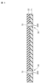
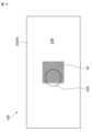
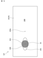
- FIG. 1 is a plan view of an electronic component according to an embodiment of the invention
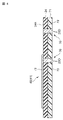
- FIG. FIG. 2 is a sectional view showing the AA section of FIG. 1
- FIG. 4 is a cross-sectional view when an interlayer connection conductor is formed on a substrate in the method of manufacturing an electronic component according to the embodiment of the present invention
- FIG. 4 is a cross-sectional view when internal electrodes are printed on a substrate in the method for manufacturing an electronic component according to the embodiment of the present invention
- FIG. 4 is a cross-sectional view showing a process of printing a mark on a substrate in the method of manufacturing an electronic component according to the embodiment of the present invention
- FIG. 2 is a cross-sectional view when a plurality of base materials are laminated to form an element body in the method for manufacturing an electronic component according to the embodiment of the present invention;
- An electronic component comprises body and a mark formed on the outer surface of the base body, A concave portion is formed on the outer surface of the element body, A portion of the mark is formed in the recess.
- part of the mark is formed in the recess. Therefore, a part of the mark and a part other than the part of the mark can have different depths. This makes it possible to change the appearance of the mark according to each position within the mark. For example, when the mark is illuminated, locations corresponding to recesses within the mark appear darker than locations corresponding to non-recesses within the mark. Due to this difference in appearance, the mark can be recognized as non-rotationally symmetric when factors other than shape such as brightness, color and pattern are included. As a result, the orientation of the electronic component can be determined based on the position of the mark.
- part of the mark is formed in the recess. Therefore, when the mark is illuminated with light, the position corresponding to the recess in the mark appears darker than the position corresponding to the portion other than the recess in the mark. As a result, a difference in density occurs between the position corresponding to the recess in the mark and the position not corresponding to the recess in the mark. As a result, the visibility of the mark can be improved.
- a portion of the mark formed in the concave portion may be asymmetric with respect to a center point of rotational symmetry of the mark when viewed from an orthogonal direction perpendicular to the outer surface of the base body.
- the portion of the mark formed in the recess is symmetrical with respect to the center point of the rotational symmetry of the mark when viewed from the orthogonal direction, the position corresponding to the recess in the mark and the position corresponding to the portion other than the recess in the mark
- the mark cannot be recognized as rotationally symmetric due to the difference in appearance from .
- the portion of the mark formed in the recess is asymmetric with respect to the center point of the rotational symmetry of the mark. Therefore, the mark can be recognized as non-rotationally symmetrical when factors other than shape such as brightness, color and pattern are included.
- the shape of the mark may be different from the shape of the recess when viewed from an orthogonal direction perpendicular to the outer surface of the base body.
- the difference between the portion formed in the concave portion and the portion formed in the non-concave portion of the mark can be made clearer than the configuration in which the shape of the mark and the shape of the concave portion are the same when viewed from the orthogonal direction. can be done. Thereby, the visibility of the mark can be improved.
- the concave portion when viewed from an orthogonal direction orthogonal to the outer surface of the base body, the concave portion includes a portion of the outer surface of the base body where the mark is formed and the mark of the outer surface of the base body. may be formed across the portion where is not formed.
- the concave portion can be made larger than the configuration in which the concave portion is formed only in the portion where the mark is formed. This makes it easy to form the recesses in the element.
- the concave portion may be formed only in a portion of the outer surface of the element where the mark is formed, when viewed from an orthogonal direction perpendicular to the outer surface of the element.
- the recess is not formed outside the mark.
- the part for forming the mark and the part for forming the recess can be made common. Therefore, the electronic component can be miniaturized.
- a plurality of recesses may be formed on the outer surface of the base body.
- the position corresponding to the recess in the mark appears darker than the position corresponding to the portion other than the recess in the mark.
- a plurality of recesses are formed on the outer surface of the base body. Therefore, a plurality of dark-looking portions are formed in the mark. As a result, a large number of bright and dark boundaries can be formed in the mark. As a result, the visibility of the mark can be improved.
- the depth of the recess along the orthogonal direction perpendicular to the outer surface of the base body may be greater than or equal to the thickness of the mark along the orthogonal direction perpendicular to the outer surface of the base body.
- the depth of the recess in the orthogonal direction is greater than or equal to the thickness of the mark in the orthogonal direction. Therefore, the visibility of the mark can be enhanced by the configuration in which the depth of the concave portion along the orthogonal direction is smaller than the thickness of the mark along the orthogonal direction.
- the mark may have a rotationally symmetrical shape when viewed from an orthogonal direction orthogonal to the outer surface of the element body, and the mark may have a rotationally symmetric shape when viewed from an orthogonal direction orthogonal to the outer surface of the element body
- the outer surface may have a rotationally symmetrical shape, and when viewed from an orthogonal direction perpendicular to the outer surface of the element body, the center point of rotational symmetry of the mark coincides with the center point of rotational symmetry of the outer surface of the element body. They may substantially match.
- the mark and the outer surface of the base body have rotationally symmetric shapes when viewed in the orthogonal direction, and the center point of the rotational symmetry of the mark when viewed in the orthogonal direction coincides or substantially coincides with the center point of the rotational symmetry of the outer surface of the base body. Even with the configuration, the following effects can be obtained. As described above, a mark with a rotationally symmetrical shape can be recognized as non-rotationally symmetrical in terms of factors other than shape, such as brightness, color, and pattern, depending on how it looks when illuminated. . As a result, the orientation of the electronic component can be determined based on the position of the mark on the base body.
- the element body may be made of ceramic.
- FIG. 1 is a plan view of an electronic component according to an embodiment of the invention.
- FIG. 2 is a cross-sectional view showing the AA cross section of FIG.
- the electronic component has a mark provided on the base body.
- an internal conductor and an external electrode are provided on the base body.
- Electronic components can be mounted on a mother board or the like via external electrodes.
- the electronic component 10 includes a base body 20, interlayer connection conductors 30, internal electrodes 40, external electrodes 50, plating layers 55, and identification marks 60.
- the identification mark 60 is an example of a mark.
- the element body 20 has a rectangular parallelepiped shape as a whole.
- the shape of the element body 20 is not limited to a rectangular parallelepiped shape.
- the element body 20 is formed by integrating laminated base materials 22 to 28 . Note that the number of base materials constituting the base body 20 is not limited to seven.
- Each of the substrates 22-28 is insulative and plate-shaped.
- the element body 20 (each base material 22 to 28) is made of LTCC (Low Temperature Co-fired Ceramics).
- the base body 20 is not limited to LTCC, and may be made of ceramics other than LTCC such as alumina, or may be made of resin such as glass epoxy, Teflon (registered trademark), or paper phenol.
- the element body 20 is a sintered body of the same material, there is no interface between the base materials 22-28.
- dashed lines are drawn between the substrates 22 to 28 for convenience of explanation.
- an interface may remain at the location indicated by the dashed line in FIG.
- the base body 20 has main surfaces 20A and 20B and side surfaces 20C.
- the main surface 20A is the main surface of the base material 22 and faces the outside of the element body 20 .
- the main surface 20B is the main surface of the base material 28 and faces the outside of the element body 20 .
- the principal surface 20B faces away from the principal surface 20A.
- the side surface 20C is composed of side surfaces of the substrates 22-28. The side surface 20C connects the main surfaces 20A and 20B.
- the plan view of FIG. 1 is a diagram when the electronic component 10 is viewed from the orthogonal direction 100 (see FIG. 2).
- the orthogonal direction 100 is a direction orthogonal to the main surface 20B of the element body 20 .
- the orthogonal direction 100 is the direction orthogonal to the identification mark 60 .
- the main surface 20B of the element body 20 when viewed from the orthogonal direction 100, is rectangular. That is, in the present embodiment, when viewed from the orthogonal direction 100, the main surface 20B of the base body 20 has a rotationally symmetrical shape with the rotation center as the center point 20Ba.
- the main surface 20B of the element body may have a non-rotationally symmetrical shape when viewed in the orthogonal direction 100, such as a T shape when viewed in the orthogonal direction 100.
- FIG. 1 is a diagram when the electronic component 10 is viewed from the orthogonal direction 100 (see FIG. 2).
- the orthogonal direction 100 is a direction orthogonal
- the main surface 20B of the element body 20 is formed with a recess 20E.
- the recess 20E is formed on the surface on which the identification mark 60 is formed.
- the identification mark 60 is formed on the main surface 20B of the base body 20, as will be described later. Therefore, the recess 20E is formed on the main surface 20B of the base body 20.
- the surface on which the concave portion 20E is formed corresponds to the outer surface of the element. That is, in this embodiment, the main surface 20B of the element body 20 corresponds to the outer surface of the element body.
- the recess 20E may be formed on a surface other than the main surface 20B of the element.
- the recess 20E is formed on the main surface 20A of the base body.
- the recess 20E may be formed on both the principal surfaces 20A and 20B of the element body 20. may be formed on one of the main surfaces 20A and 20B of the . That is, when electronic component 10 has identification mark 60 on each of a plurality of surfaces, recess 20E is formed on at least one of the plurality of surfaces.
- the recess 20E is spherical.
- the surface forming the recess 20E is a spherical surface. That is, as shown in FIG. 1, the concave portion 20E has a circular shape when viewed from the orthogonal direction 100.
- the shape of the recess 20E is not limited to a spherical shape.
- the recess 20E may have a rectangular parallelepiped shape. In this case, when viewed from the orthogonal direction 100, the recess 20E is rectangular.
- the interlayer connection conductor 30 is formed inside the element body 20. As shown in FIG. 2, the interlayer connection conductor 30 may be formed on at least one of substrates 22-28. In this embodiment, the interlayer connection conductors 30 are formed on the substrates 22-26.
- the interlayer connection conductor 30 is made of a ceramic (LTCC in this embodiment) filled with a conductive paste in a through hole 20D penetrating through at least one of the plurality of substrates 22 to 28 in the thickness direction of the substrates 22 to 28. It is co-fired.
- the conductive paste contains conductive powder such as copper.
- the conductive powder contained in the conductive paste is not limited to copper, and may be silver, for example.
- the interlayer connection conductor 30 is formed by plating a conductive metal made of copper or the like.
- the interlayer connection conductor 30 since the through hole 20D has a columnar shape, the interlayer connection conductor 30 has a columnar shape.
- the shape of the through-hole 20 ⁇ /b>D is not limited to a cylindrical shape, and may be, for example, a quadrangular prism shape.
- the interlayer connection conductor 30 includes four interlayer connection conductors 31-34.
- the interlayer connection conductor 31 is filled in the through hole 20D penetrating through the substrates 24-26.
- the interlayer connection conductor 32 is filled in the through hole 20 ⁇ /b>D passing through the substrates 25 and 26 .
- the interlayer connection conductor 33 is filled in the through hole 20D penetrating through the substrates 22-26.
- the interlayer connection conductor 34 is filled in the through hole 20 ⁇ /b>D passing through the substrates 22 and 23 .
- the number of interlayer connection conductors 30 is not limited to four.
- the length in the thickness direction of each of the interlayer connection conductors 31 to 34 (the number of substrates that penetrate through) is not limited to the length described above.
- the internal electrodes 40 are formed inside the element body 20 and are not exposed to the outside of the element body 20 .
- Internal electrodes 40 may be formed on at least one of substrates 22-28.
- the internal electrodes 40 are formed on the main surface 24A of the base material 24, the main surface 25A of the base material 25, and the main surface 27A of the base material 27. As shown in FIG.
- the internal electrodes 40 are formed by printing a conductive paste on the main surfaces of the substrate (main surfaces 24A, 25A and 27A in this embodiment). , which is co-fired with the substrate.
- the conductive paste is composed of copper or silver, for example.
- the internal electrodes 40 are formed on the main surface of the base material by known means such as etching a metal foil.
- the internal electrode 40 includes four internal electrodes 41-44.
- the internal electrodes 41 are formed on the main surface 24A of the base material 24.
- the internal electrodes 42 are formed on the main surface 25A of the base material 25 .
- the internal electrodes 43 and 44 are formed on the main surface 27A of the base material 27. As shown in FIG.
- Each internal electrode 40 is electrically connected to other internal electrodes 40 and external electrodes 50 via interlayer connection conductors 30 .
- the internal electrodes 41 and 43 are electrically connected to each other via the interlayer connection conductor 31 .
- the internal electrodes 42 and 44 are electrically connected to each other via the interlayer connection conductor 32 .
- each of the internal electrodes 41 and 43 is electrically connected to an external electrode 50 to be described later via interlayer connection conductors 33 and 34 .
- the external electrode 50 is formed outside the element body 20 . That is, the external electrodes 50 are exposed outside the element body 20 .
- the external electrodes 50 are formed on the main surface of the base material 22 , that is, on the main surface 20A of the element body 20 .
- the external electrodes 50 may be formed on the main surface of the base material 28 , that is, on the main surface 20B of the element body 20 .
- the external electrode 50 is configured in the same manner as the internal electrode 40 . That is, in this embodiment, the external electrodes 50 are formed by printing a conductive paste on the main surface 20A of the element body 20 and co-firing it with the substrates 22-28. In this embodiment, the electronic component 10 has two external electrodes 50 . As described above, each external electrode 50 is electrically connected to each internal electrode 41 , 43 .
- the plating layer 55 covers the external electrodes 50 .
- the plating layer 55 suppresses the influence of the atmosphere, moisture, etc. on the external electrodes 50 .
- the plated layer 55 is, for example, a film made of Ni—Sn, Ni—electroless Au, or the like. Although two plating layers 55 are depicted in FIG. 2 , the number of plating layers 55 provided in electronic component 10 is not limited to two.
- the identification mark 60 is formed on the base body 20.
- the identification mark 60 is for indicating the posture and direction of the electronic component 10 .
- the identification mark 60 is formed on the main surface 20B of the element body 20, which is the outer surface of the element body 20. As shown in FIG. Note that the identification mark 60 may be formed on another outer surface of the element body 20, for example, the main surface 20A of the element body.
- the electronic component 10 has one identification mark 60 in this embodiment, it may have a plurality of identification marks 60 .
- the color of the identification mark 60 is shown in gray in each drawing, the color of the identification mark 60 is not limited to gray, and may be other colors such as black and red.
- the identification mark 60 is embedded in the base body 20. It should be noted that the outer surface of the identification mark 60 does not have to enter the base body 20 . For example, the identification mark 60 may protrude with respect to the main surface 20B of the element body 20 by only partially entering the element body 20 .
- the identification mark 60 is composed of a material different from that of the base body 20.
- the identification mark 60 is made of a non-conductive inorganic material (eg, ceramic).
- the identification mark 60 is not limited to ceramic, and may be made of, for example, resin or a conductive member (eg, metal such as copper or silver). Also, the visibility of the identification mark 60 may be improved by making the ceramic a different color from that of the element body 20 . For example, oxide ceramics such as alumina, zirconia, cobalt, etc. may be mixed to change the color. Also, the identification mark 60 may be composed of a plurality of types of materials. For example, the identification mark 60 may be composed of a main material having the highest proportion among constituent materials and at least one other material having a lower proportion than the main material. In this case, for example, other materials of the identification mark 60 are added to the main material of the identification mark 60 , such as glass or a component similar to LTCC, which is the material of the base body 20 .
- LTCC which is the material of the base body 20 .
- the identification mark 60 has a circular shape when viewed from the orthogonal direction 100 . That is, in the present embodiment, the identification mark 60 has a rotationally symmetrical shape with the center point 60A as the center of rotation when viewed from the orthogonal direction 100 . In this embodiment, when viewed from the orthogonal direction 100, the rotationally symmetrical center point 60A of the identification mark 60 and the rotationally symmetrical center point 20Ba of the main surface 20B of the base body 20 coincide.
- the shape of the identification mark 60 when viewed from the orthogonal direction 100 is not limited to circular, and may be rectangular, for example.
- the rotationally symmetrical center point 60A of the identification mark 60 and the rotationally symmetrical center point 20Ba of the main surface 20B of the base body 20 do not need to match completely.
- the two center points 60 ⁇ /b>A and 20 ⁇ /b>Ba may differ by an error during formation of the identification mark 60 and a tolerance of the base body 20 . That is, when viewed from the orthogonal direction 100, the two center points 60A and 20Ba may substantially coincide.
- the recess 20E of the base body 20 when viewed from the orthogonal direction 100, the recess 20E of the base body 20 is circular as described above. Further, when viewed from the orthogonal direction 100, the recess 20E of the base body 20 has the same size as the identification mark 60. As shown in FIG.
- the center point 20Ea of the concave portion 20E is located at a position different from the rotationally symmetrical center point 60A of the identification mark 60. That is, the concave portion 20E is formed at a position shifted from the identification mark 60.
- part of the identification mark 60 overlaps part of the recess 20E of the base body 20.
- part of the identification mark 60 is formed in the recess 20E of the base body 20.
- the concave portion 20E of the element body 20 is formed by the portion of the principal surface 20B of the element body 20 where the identification mark 60 is formed and the identification mark of the principal surface 20B of the element body 20. 60 is formed straddling the portion where it is not formed.
- the portion of the identification mark 60 formed in the recess 20E (the hatched portion in FIG. 1, hereinafter referred to as the overlapping portion 60B) ) are asymmetrical with respect to the rotationally symmetric center point 60A of the identification mark 60 .
- the depth D of the concave portion 20E along the orthogonal direction 100 is greater than the thickness T of the identification mark 60 along the orthogonal direction 100.
- the depth D of the recess 20E is the maximum depth among the depths of the respective positions.
- the thickness T of the identification mark 60 is the maximum thickness among the thicknesses at each position.
- the depth D is 6 to 7 ( ⁇ m) and the thickness T is 5 ( ⁇ m).
- the depth D and thickness T are not limited to the above values.
- the depth D of the concave portion 20E along the orthogonal direction 100 may be the same as the thickness T of the identification mark 60 along the orthogonal direction 100, or smaller than the thickness T of the identification mark 60 along the orthogonal direction 100.
- part of the identification mark 60 is formed in the recess 20E. Therefore, a part of the identification mark 60 and a part other than the part of the identification mark 60 can have different depths. Thereby, the appearance of the identification mark 60 can be changed according to each position within the identification mark 60 . For example, when the identification mark 60 is illuminated, the position corresponding to the recess 20E in the identification mark 60 looks darker than the position corresponding to other than the recess 20E in the identification mark 60. FIG. Due to this difference in appearance, the identification mark 60 can be recognized as non-rotationally symmetrical when factors other than shape, such as brightness, color, and pattern, are included. As a result, the orientation of electronic component 10 can be determined based on the position of identification mark 60 .
- part of the identification mark 60 is formed in the recess 20E. Therefore, when the identification mark 60 is illuminated, the position corresponding to the recess 20E in the identification mark 60 looks darker than the position corresponding to the portion other than the recess 20E in the identification mark 60. FIG. As a result, a difference in density occurs between a position corresponding to the recess 20E in the identification mark 60 and a position not corresponding to the recess 20E in the identification mark 60. FIG. As a result, the visibility of the identification mark 60 can be improved.
- the center point 20Ea of the recess 20E coincides with the rotationally symmetrical center point 60A of the identification mark 60
- the portion of the identification mark 60 formed in the recessed portion 20E is aligned with the rotationally symmetrical center point 60A of the identification mark 60.
- the portion of the identification mark 60 formed in the recess 20E is asymmetric with respect to the center point 60A of the rotational symmetry of the identification mark 60.
- FIG. Therefore, the identification mark 60 can be recognized as non-rotationally symmetrical when factors other than the shape such as brightness, color and pattern are included.
- the concave portion 20E when viewed from the orthogonal direction 100, the concave portion 20E is a portion of the principal surface 20B of the element body 20 where the identification mark 60 is formed and the identification mark of the principal surface 20B of the element body 20. 60 is formed straddling the portion where it is not formed. Therefore, the concave portion 20E can be made larger than the configuration in which the concave portion 20E is formed only in the portion where the identification mark 60 is formed. This makes it easy to form the recesses 20E in the element body 20 .
- the depth D along the orthogonal direction 100 of the recess 20E is greater than the thickness T along the orthogonal direction 100 of the identification mark 60 . Therefore, the visibility of the identification mark 60 can be enhanced by the configuration in which the depth D of the concave portion 20E along the orthogonal direction 100 is smaller than the thickness T of the identification mark 60 along the orthogonal direction 100.
- the identification mark 60 and the main surface 20B of the base body 20 when viewed in the orthogonal direction 100 each have a rotationally symmetrical shape, and the central point 60A of the rotational symmetry of the identification mark 60 when viewed in the orthogonal direction 100 is the main surface of the base body 20.
- the following effects are obtained even with a configuration that coincides or substantially coincides with the rotationally symmetric center point 20Ba of 20B.
- the identification mark 60 which has a rotationally symmetrical shape, is recognized as non-rotationally symmetrical in terms of factors other than shape such as brightness, color, and pattern, depending on how it looks when illuminated. can do.
- the orientation of the electronic component 10 can be determined based on the position of the identification mark 60 on the base body 20 .
- the area of the overlapping portion 60B when viewed from the orthogonal direction 100, the area of the overlapping portion 60B (the hatched portion in FIG. % to 70%. That is, in the present embodiment, the lower limit of the ratio of the area of the overlapping portion 60B to the area of the identification mark 60 when viewed from the orthogonal direction 100 is 30% of the area of the identification mark 60. FIG. Further, in this embodiment, the upper limit of the ratio of the area of the overlapping portion 60B to the area of the identification mark 60 when viewed from the orthogonal direction 100 is 70% of the area of the identification mark 60.
- the above lower limit is not limited to 30%, and the above upper limit is not limited to 70%.
- the above lower limit and upper limit can be different values depending on the size, shape, etc. of the identification mark 60 .
- the lower limit may be lower than 30% (eg 20%) or higher than 30% (eg 40%).
- the upper limit may be higher than 70% (eg 80%) or lower than 70% (eg 60%).
- the appropriate value for example, 30%
- the area of the overlapping portion 60B viewed from the orthogonal direction 100 is too small, and the visibility of the overlapping portion 60B with respect to other portions of the identification mark 60 other than the overlapping portion 60B is improved. not sufficiently effective.
- the visibility improvement effect is that, for example, when the identification mark 60 is exposed to light, the overlapping portion 60B looks darker than other portions, thereby improving the visibility of the identification mark 60 .
- the above lower limit is lower than the appropriate value
- the area of the overlapped portion 60B as viewed from the orthogonal direction 100 is too small, and there is a possibility that the shape of the overlapped portion 60B cannot be sufficiently determined with respect to other portions.
- the identification mark 60 looks dark as a whole, so that the difference in shading with other than the identification mark 60 becomes clear, and the visibility of the identification mark 60 as a whole is improved.
- the area of the overlapping portion 60B as viewed in the orthogonal direction 100 is too large relative to the area of the other portions, there is a possibility that the shape of the overlapping portion 60B cannot be sufficiently determined.
- FIG. 3 is a cross-sectional view when an interlayer connection conductor is formed on a substrate in the method of manufacturing an electronic component according to the embodiment of the present invention.
- FIG. 4 is a cross-sectional view when internal electrodes are printed on a base material in the electronic component manufacturing method according to the embodiment of the present invention.
- FIG. 5 is a cross-sectional view showing a process of printing an identification mark on a substrate in the method of manufacturing an electronic component according to the embodiment of the present invention.
- FIG. 6 is a cross-sectional view when a base body is formed by laminating a plurality of base materials in the method of manufacturing an electronic component according to the embodiment of the present invention.
- the electronic component 10 is manufactured by singulating the laminate into a plurality of element bodies 20 .
- the laminate is formed by integrating a plurality of element bodies 20 in an arrayed state. 3 to 6 show only a portion of the laminate corresponding to one element body 20 for convenience of explanation.
- the method for manufacturing the electronic component 10 according to the present embodiment includes a sheet forming process, an interlayer connection conductor forming process, an electrode forming process, an identification mark forming process, an element forming process, a singulation process, a firing process, and a plating layer forming process. including.
- a sheet forming process is performed.
- the substrates 22 to 28 shown in FIG. 2 are individually formed.
- the base materials 22 to 28 formed in the sheet forming process are prepared by mixing raw materials including a main material, a plasticizer, a binder, etc. corresponding to each base material 22 to 28, thereby forming a slurry forming each base material 22 to 28. is produced.
- Each of the substrates 22-28 at this stage is a green sheet made up of slurry.
- sinterable ceramic powder or the like is used as the main material for each of the base materials 22-28.
- a plasticizer for example, a phthalate ester, di-n-butyl phthalate, or the like is used.
- a binder for example, acrylic resin, polyvinyl butyral, or the like is used.
- the slurry forming each of the base materials 22 to 28 is formed into a sheet on the carrier film 71 shown in FIG. 3 using, for example, a lip coater or doctor blade. That is, each of the seven substrates 22 to 28 is molded on each of the seven carrier films 71 .
- the carrier film 71 for example, a PET (polyethylene terephthalate) film or the like is used.
- the thickness of each of the substrates 22-28 is, for example, 5-100 ( ⁇ m).
- FIG. 3 shows the carrier film 71 and the base material 22 molded on the carrier film 71 .
- through-holes 20D are formed through the base materials 22 to 28 and the carrier film 71 in the thickness direction.
- the number of through holes 20D formed in each of the substrates 22 to 28 is not limited to two. Also, the number of through-holes 20D formed in the seven substrates 22 to 28 and the carrier film 71 may be the same or different. Also, the number of through holes 20D formed in the seven substrates 22 to 28 and the carrier film 71 may be the same or different.
- the penetrations formed in the seven substrates 22 to 28 and the carrier film 71 are finally formed so that the element body 20 as shown in FIG.
- the number and location of holes 20D are determined.
- interlayer connection conductor forming step Next, an interlayer connection conductor forming step is performed.
- the through holes 20D formed in the base materials 22 to 28 and the carrier film 71 in the sheet forming process are filled with a conductive paste 72 (see FIG. 3).
- the paste 72 is made, for example, by mixing raw materials including conductive powder, a plasticizer, and a binder.
- Electrode forming step Next, an electrode forming process is performed. In the electrode forming process, the external electrodes 50 and the internal electrodes 40 are formed.
- the paste 73 is formed by screen printing, inkjet printing, gravure printing, or the like, for example.
- the internal electrodes 42 to 44 and the external electrode 50 are also formed on the respective substrates 22, 25 and 27 in the same manner as the internal electrode 41.
- the paste 73 is made by mainly mixing raw materials including conductive powder, plasticizer, and binder, similarly to the paste 72 described above.
- the paste 73 may be made of the same material as the paste 72 or may be made of a material different from that of the paste 72 .
- the identification mark forming process includes a first printing process and a second printing process.
- a method for manufacturing an electronic component 10 includes a first printing step of printing an identification mark on a main surface of a base material to be printed with a mark, which is one of a plurality of base materials, and a part of the identification mark. a second printing step of printing a non-sinterable paste on the area of or on the area covering both a part of the main surface of the substrate to be printed with the mark and a part of the identification mark; including.
- the identification mark forming process will be described below with reference to FIG. In FIG. 5, the identification mark forming process is divided into two stages.
- the upper side of the paper surface of FIG. 5 is the first stage, and the lower side of the paper surface of FIG. 5 is the second stage.
- a paste 74 corresponding to the identification mark 60 is formed on the main surface 20B of the base material 28.
- the base material 28 is an example of a base material on which marks are printed.
- the paste 74 is formed by screen printing, inkjet printing, gravure printing, or the like, for example.
- the paste 74 is made of the material forming the identification mark 60 described above.
- the paste 75 is a paste of ceramic.
- the identification mark 60 is printed on the main surface 20B of the base material 28 in the first stage.
- the first stage corresponds to the first printing process of the identification mark forming process.
- the paste 75 is formed on the main surface 20B of the base material 28 .
- the material of the paste 75 a material that is burnt off during firing, which will be described later, is used.
- the material of the paste 75 is non-sinterable resin.
- the paste 75 is formed by, for example, screen printing, inkjet printing, gravure printing, etc., similarly to the paste 74 .
- the paste 75 is formed on a region covering both a portion of the main surface 20B of the base material 28 and a portion of the paste 74 formed in the first stage. As can be seen, in a second step, a non-sinterable paste 75 is printed over said areas.
- the second stage corresponds to the second printing process of the identification mark forming process.
- the paste 75 serves as a base for the recesses 20E of the base body 20. Therefore, the paste 75 is printed on the main surface 20B of the base material 28 in areas corresponding to the recesses 20E. For example, when forming the concave portion 20E as shown in FIG. be done. Further, for example, when forming a concave portion 20E as shown in FIG.
- a body forming step is performed.
- the plurality of A body forming step is included in which the base materials are laminated together to form a body.
- each of the base materials 22 to 28 excluding the carrier film 71 is laminated and pressed in a mold. Thus, the base body 20 is obtained.
- the seven substrates 22 to 28 are arranged in order from substrates with smaller reference numerals to substrates with larger reference numerals, specifically substrates 22, 23, 24, 25, and 26. , 27 and 28 are stacked.
- the main surface 20A of the base material 22 and the main surface 20B of the base material 28 become the outer surfaces of the element body 20 .
- the plurality of base materials 22 to 28 are laminated together so that the main surface 20B of the base material 28 is exposed.
- the external electrodes 50 enter the base material 22 and the identification mark 60 and the paste 75 enter the base material 28 by pressing the base materials 22 to 28 together.
- the plurality of base materials 22 to 28 are stacked one on top of the other such that the identification mark 60 and the paste 75 are embedded in the base material 28 .
- a singulation process is performed.
- a laminate in which a plurality of element bodies 20 are arranged is cut into a plurality of element bodies 20 .
- a dicing saw, a guillotine cutter, a laser, or the like, for example, is used to cut the laminate.
- the corners and edges of the blank 20 may be polished, such as by barreling. Note that the polishing may be performed after the firing process.
- the method of manufacturing the electronic component 10 according to the present embodiment includes a firing step of firing the body and removing the resin paste.
- each of the base materials 22 to 28 forming the element body 20 is cured. That is, each of the substrates 22-28, which are flexible green sheets, are cured and transformed into substrates.
- the paste 75 is burned off by firing the element body 20 .
- recesses 20E are formed where the paste 75 was present (see FIG. 2).
- the method of forming the recess 20E is not limited to the method of burning off the paste 75 as described above.
- the recesses 20E may be formed in the element body 20 by pressing the element body 20 with a mold having projections.
- plating layer forming step Next, a plating layer forming step is performed. In the plating layer lamination step, the external electrodes 50 are subjected to a known plating process. As a result, the plating layer 55 is formed to completely cover the external electrodes 50, as shown in FIG.
- the plating layer 55 may be formed so as to cover only a part of the external electrode 50 .
- the plating layer 55 may be formed so as to cover the main surface 20 ⁇ /b>A around the external electrodes 50 .
- the paste 75 that has entered the base material 28 in the element forming process is removed by the firing process.
- the concave portion 20E can be formed in a region including at least a part of the identification mark 60 in the principal surface 20B of the base material 28 .
- both the identification mark 60 and the recess 20E are circular (same shape) and the same size when viewed from the orthogonal direction 100 . Also, when viewed from the orthogonal direction 100, a portion of the identification mark 60 and a portion of the recess 20E overlap each other.
- the identification mark 60 and the concave portion 20E are not limited to the configurations described above. Modifications of the electronic component 10 according to the embodiment will be described below.
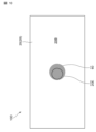
- FIG. 7 is a plan view of an electronic component according to Modification 1 of the embodiment of the invention.
- the identification mark 60 may have a different size than the recess 20E.
- both the identification mark 60 and the recess 20E are circular and have the same shape when viewed from the orthogonal direction 100. less than 60 Contrary to the above, the concave portion 20E may be larger than the identification mark 60.
- FIG. 7 is a plan view of an electronic component according to Modification 1 of the embodiment of the invention.
- the identification mark 60 may have a different size than the recess 20E.
- both the identification mark 60 and the recess 20E are circular and have the same shape when viewed from the orthogonal direction 100. less than 60 Contrary to the above, the concave portion 20E may be larger than the identification mark 60.
- FIG. 8 is a plan view of an electronic component according to Modification 2 of the embodiment of the present invention.
- FIG. 9 is a plan view of an electronic component according to Modification 3 of the embodiment of the present invention.
- the identification mark 60 and the recess 20E may have different shapes.
- the identification mark 60 in the electronic component 10B according to Modification 2, the identification mark 60 has a rectangular shape and the concave portion 20E has a circular shape when viewed from the orthogonal direction 100 .
- the identification mark 60 has a circular shape, while the concave portion 20E has an elliptical shape.
- the portion of the identification mark 60 formed in the recess 20E and the portion other than the recess 20E are formed.
- the difference between parts can be clarified. Thereby, the visibility of the identification mark 60 can be improved.
- FIG. 10 is a plan view of an electronic component according to Modification 4 of the embodiment of the present invention.
- the concave portion 20E of the base body 20 is the portion of the main surface 20B of the base body 20 where the identification mark 60 is formed and the base body. It is formed across a portion of the main surface 20B of the body 20 where the identification mark 60 is not formed.
- the concave portions 20E of the base body 20 are formed in the portion of the main surface 20B of the base body 20 where the identification mark 60 is formed. ing. That is, in the electronic component 10D, the recess 20E of the base body 20 is formed only in the portion of the main surface 20B of the base body 20 where the identification mark 60 is formed. Further, in the electronic component 10D, the concave portion 20E of the base body 20 occupies a part of the identification mark 60. As shown in FIG. That is, the identification mark 60 consists of a portion formed in the recess 20E of the main surface 20B of the element body 20 and a portion formed in the main surface 20B of the element body 20 other than the recess 20E.
- the recess 20E is not formed outside the identification mark 60.
- the portion for forming the identification mark 60 and the portion for forming the concave portion 20E can be made common. Therefore, the electronic component 10 can be miniaturized.
- FIG. 11 is a plan view of an electronic component according to Modification 5 of the embodiment of the present invention.
- main surface 20B of element body 20 is formed with a plurality of recesses 20E.
- main surface 20B of element body 20 is formed with four recesses 20Eb, 20Ec, 20Ed, and 20Ee.
- a portion of each of the recesses 20Eb, 20Ec, and 20Ed overlaps the identification mark 60 when viewed from the orthogonal direction 100 .
- All of the concave portions 20Ee overlap the identification mark 60 when viewed from the orthogonal direction 100 .
- the number of recesses 20E is not limited to four.
- the shape of the plurality of recesses 20E is not limited to a circular shape.
- the size of each recess 20E may be the same, or may be different from each other.
- FIG. 11 when viewed from the orthogonal direction 100, each of the three recesses 20Eb, 20Ec, and 20Ed partially overlaps the identification mark 60, and the recess 20Ee entirely overlaps the identification mark 60. , but not limited to this.
- all of the recesses 20E may partially overlap the identification mark 60.
- all of the plurality of recesses 20E may be formed within the identification mark 60 when viewed from the orthogonal direction 100 .
- the position corresponding to the recess 20E within the identification mark 60 appears darker than the position corresponding to the portion other than the recess 20E within the identification mark 60.
- the main surface 20B of the element body 20 is formed with a plurality of recesses 20E. Therefore, a plurality of dark-looking portions are formed in the identification mark 60 . As a result, a large number of bright and dark boundaries can be formed in the identification mark 60 . As a result, the visibility of the identification mark 60 can be improved.
- FIG. 12 is a plan view of an electronic component according to Modification 6 of the embodiment of the present invention.
- FIG. 13 is a plan view of an electronic component according to Modification 7 of the embodiment of the invention.
- the overlapping portion 60B (the hatched portion in FIG. 1) of the identification mark 60 formed in the concave portion 20E serves as an identification It is asymmetric with respect to the center point 60A of rotational symmetry of the mark 60 .
- the recess 20E of the identification mark 60 has The overlapping portion 60B (the hatched portion in FIGS. 12 and 13) is symmetrical about the center point 60A of rotational symmetry of the identification mark 60. As shown in FIG.
- the rotationally symmetrical center point 60A of the identification mark 60 is located at a position different from the rotationally symmetrical center point 20Ba of the main surface 20B of the base body 20.
- the orientation of the electronic component 10 can be determined based on the position of the identification mark 60 .
- the identification mark 60 is illuminated with light, the overlapping portion 60B of the identification mark 60 formed in the concave portion 20E appears darker than the other portions of the identification mark 60 . Thereby, the visibility of the identification mark 60 can be improved.
- the rotational symmetry center point 60A of the identification mark 60 and the rotational symmetry center point 20Ba of the main surface 20B of the base body 20 are different from each other when viewed from the orthogonal direction 100.
- an identification mark 60 may be formed.
Landscapes
- Engineering & Computer Science (AREA)
- Power Engineering (AREA)
- Microelectronics & Electronic Packaging (AREA)
- Manufacturing & Machinery (AREA)
- Structure Of Printed Boards (AREA)
- Details Of Resistors (AREA)
Abstract
マークの視認性を高めつつ、素体におけるマークの位置に基づいて部品の方向を判別することができる電子部品を提供する。電子部品は、素体と、素体の主面に形成されたマークと、素体の主面に形成された凹部とを備える。マークの一部は、凹部の一部に形成されている。これにより、素体の主面と直行する方向から見て、マークの一部と凹部の一部とが重複している。
Description
本発明は、素体と当該素体の外面に形成されたマークとを備える電子部品及びその製造方法に関する。
素体と当該素体の外面に形成されたマークとを備える電子部品の一例として、特許文献1には、部品の方向を示すマーカー部を備える受動電子部品が開示されている。
特許文献1に開示された受動電子部品では、マークに対応するマーカー部が素体に対応する絶縁体部の外面の中央部からずれた位置に形成されていたり、マーカー部が三角形等の非対称な形状であったりすることによって、部品の方向が判別可能である。
マークは、例えばカメラ等によって読み取られる。マークが素体の外面の中央部からずれた位置に形成されている場合、マークの位置が読み取られることによって、部品の方向が判別される。しかし、マークが素体の外面の中央部に形成されている場合、マークの位置では、部品の方向が判別できないおそれがある。
マークが非対称な形状である場合、マークが素体の外面の中央部に形成されていたとしても、マークの形状が読み取られることによって、部品の方向が判別可能である。しかし、マークの形状の読み取りは、マークの位置の読み取りより、高い読み取り精度が要求される。そのため、マークの形状を読み取ることによって部品の方向を判別するより、マークの位置を読み取ることによって部品の方向を判別することが望ましい。
また、素体のサイズが小さい場合、マークが形成されるスペースが制限される。また、マークが素体に形成された電極等と干渉するおそれがある。これらの問題の解決のため、マークのサイズを小さくすることが考えられる。しかし、マークを小さくすることによって、マークの視認性が低下するおそれがある。
従って、本発明の目的は、前記課題を解決することにあって、マークの視認性を高めつつ、素体におけるマークの位置に基づいて部品の方向を判別することができる電子部品を提供することにある。
前記目的を達成するために、本発明は以下のように構成する。
本発明の一態様に係る電子部品は、
素体と、
前記素体の外面に形成されたマークと、を備え、
前記素体の外面に、凹部が形成されており、
前記マークの一部は、前記凹部に形成されている。
本発明の一態様に係る電子部品は、
素体と、
前記素体の外面に形成されたマークと、を備え、
前記素体の外面に、凹部が形成されており、
前記マークの一部は、前記凹部に形成されている。
本発明によれば、マークの視認性を高めつつ、素体におけるマークの位置に基づいて部品の方向を判別することができる。
本発明の一態様に係る電子部品は、
素体と、
前記素体の外面に形成されたマークと、を備え、
前記素体の外面に、凹部が形成されており、
前記マークの一部は、前記凹部に形成されている。
素体と、
前記素体の外面に形成されたマークと、を備え、
前記素体の外面に、凹部が形成されており、
前記マークの一部は、前記凹部に形成されている。
この構成によれば、マークの一部は、凹部に形成される。そのため、マークの一部とマークの当該一部以外の部分とを、異なる深さとすることができる。これにより、マーク内の各位置に応じてマークの見え方を変えることができる。例えば、マークに光を当てたとき、マーク内の凹部に対応する位置は、マーク内の凹部以外に対応する位置より暗く見える。この見え方の違いによって、マークを、明るさ、色彩、模様等の形状以外の要素を含めた場合において非回転対称なものとして認識することができる。その結果、マークの位置に基づいて電子部品の方向を判別することができる。
この構成によれば、マークの一部が凹部に形成されている。そのため、マークに光を当てたとき、マーク内の凹部に対応する位置は、マーク内の凹部以外の部分に対応する位置より暗く見える。これにより、マーク内の凹部に対応する位置と、マーク内の凹部に対応しない位置とに、濃淡差が発生する。その結果、マークの視認性を高めることができる。
前記電子部品において、前記素体の外面と直交する直交方向から見て、前記マークのうちの前記凹部に形成された部分は、前記マークの回転対称の中心点に対して非対称であってもよい。
直交方向から見て、マークのうちの凹部に形成された部分がマークの回転対称の中心点に対して対称である場合、マーク内の凹部に対応する位置とマーク内の凹部以外に対応する位置との見え方の違いによっても、マークを非回転対称なものとして認識することができない。しかし、この構成によれば、マークのうちの凹部に形成された部分は、マークの回転対称の中心点に対して非対称である。そのため、マークを、明るさ、色彩、模様等の形状以外の要素を含めた場合において非回転対称なものとして認識することができる。
前記電子部品において、前記素体の外面と直交する直交方向から見て、前記マークの形状は、前記凹部の形状と異なっていてもよい。
この構成によれば、直交方向から見てマークの形状と凹部の形状とが同じである構成より、マークにおいて凹部に形成された部分と凹部以外に形成された部分との違いを明確にすることができる。これにより、マークの視認性を高めることができる。
前記電子部品において、前記素体の外面と直交する直交方向から見て、前記凹部は、前記素体の外面のうちの前記マークが形成された部分と、前記素体の外面のうちの前記マークが形成されていない部分とに跨って形成されていてもよい。
この構成によれば、マークが形成された部分のみに凹部が形成されている構成より、凹部を大きくすることができる。これにより、素体に凹部を形成することが容易である。
前記電子部品において、前記素体の外面と直交する直交方向から見て、前記凹部は、前記素体の外面のうちの前記マークが形成された部分のみに形成されていてもよい。
この構成によれば、凹部がマークの外部に形成されない。これにより、電子部品において、マークを形成するための部分と、凹部を形成するための部分とを、共通化することができる。そのため、電子部品を小型化することができる。
前記電子部品において、前記素体の外面に、複数の前記凹部が形成されていてもよい。
マークに光を当てたとき、マーク内の凹部に対応する位置は、マーク内の凹部以外の部分に対応する位置より暗く見える。この構成によれば、素体の外面には、複数の凹部が形成されている。そのため、マーク内の暗く見える箇所が複数箇所形成される。これにより、マークにおいて明暗の境界部を多数形成することができる。その結果、マークの視認性を高めることができる。
前記電子部品において、前記凹部の前記素体の外面と直交する直交方向に沿った深さは、前記マークの前記素体の外面と直交する直交方向に沿った厚み以上であってもよい。
凹部に形成されたマークに光を当てたとき、凹部が深い程、凹部に形成されたマークは暗く見える。この構成によれば、凹部の直交方向に沿った深さは、マークの直交方向に沿った厚み以上である。そのため、凹部の直交方向に沿った深さがマークの直交方向に沿った厚みより小さい構成より、マークの視認性を高めることができる。
前記電子部品において、前記素体の外面と直交する直交方向から見て、前記マークは回転対称な形状であってもよく、前記素体の外面と直交する直交方向から見て、前記素体の外面は回転対称な形状であってもよく、前記素体の外面と直交する直交方向から見て、前記マークの回転対称の中心点は、前記素体の外面の回転対称の中心点と一致または略一致していてもよい。
直交方向から見てマーク及び素体の外面がそれぞれ回転対称な形状を有し、直交方向から見てマークの回転対称の中心点が素体の外面の回転対称の中心点と一致または略一致する構成であっても、以下の効果を奏する。前述したように、光を当てたときの見え方の違いによって、回転対称な形状であるマークを、明るさ、色彩、模様等の形状以外の要素において非回転対称なものとして認識することができる。その結果、素体におけるマークの位置に基づいて電子部品の方向を判別することができる。
前記電子部品において、前記素体は、セラミックで構成されていてもよい。
<実施形態>
図1は、本発明の実施形態に係る電子部品の平面図である。図2は、図1のA-A断面を示す断面図である。電子部品は、素体にマークが設けられたものである。本実施形態に係る電子部品は、マークの他に内部導体と外部電極とが素体に設けられている。電子部品は、外部電極を介してマザー基板等に実装され得る。
図1は、本発明の実施形態に係る電子部品の平面図である。図2は、図1のA-A断面を示す断面図である。電子部品は、素体にマークが設けられたものである。本実施形態に係る電子部品は、マークの他に内部導体と外部電極とが素体に設けられている。電子部品は、外部電極を介してマザー基板等に実装され得る。
図1及び図2に示すように、本実施形態に係る電子部品10は、素体20と、層間接続導体30と、内部電極40と、外部電極50と、めっき層55と、識別マーク60とを備える。識別マーク60は、マークの一例である。
素体20は、全体として直方体形状である。素体20の形状は、直方体形状に限らない。本実施形態において、素体20は、積層された基材22~28が一体化されたものである。なお、素体20を構成する基材の数は7つに限らない。基材22~28の各々は、絶縁性であり、板状である。本施形態において、素体20(各基材22~28)は、LTCC(Low Temperature Co-fired Ceramics)で構成されている。素体20は、LTCCに限らず、例えばアルミナ等のLTCC以外のセラミックで構成されていてもよいし、ガラスエポキシ、テフロン(登録商標)、紙フェノール等の樹脂で構成されていてもよい。本実施形態の場合、素体20は同一材料の焼結体であるため各基材22~28間の界面が存在しない。図2では、説明の便宜上、各基材22~28間に破線を記している。なお、素体20が異種材料を積層して構成される場合には、図2に破線で示す箇所に界面が残ることがある。
図2に示すように、素体20は、主面20A,20Bと側面20Cとを備える。主面20Aは、基材22の主面であって素体20の外部に面している。主面20Bは、基材28の主面であって素体20の外部に面している。主面20Bは、主面20Aと反対を向いている。側面20Cは、基材22~28の側面で構成されている。側面20Cは、主面20A,20Bを繋いでいる。
図1の平面図は、電子部品10を直交方向100(図2参照)から見たときの図である。直交方向100は、素体20の主面20Bと直交する方向である。言い換えると、直交方向100は、識別マーク60と直交する方向である。図1に示すように、直交方向100から見て、素体20の主面20Bは、長方形である。つまり、本実施形態において、直交方向100から見て、素体20の主面20Bは、回転中心を中心点20Baとする回転対称な形状である。素体の主面20Bは、直交方向100から見て非回転対称な形状、例えば直交方向100から見てT字形状であってもよい。
図1及び図2に示すように、素体20の主面20Bに、凹部20Eが形成されている。凹部20Eは、識別マーク60が形成される面に形成されている。本実施形態では、後述するように、識別マーク60は素体20の主面20Bに形成されている。そのため、凹部20Eは、素体20の主面20Bに形成されている。凹部20Eが形成されている面は素体の外面に相当する。つまり、本実施形態では、素体20の主面20Bが素体の外面に相当する。
凹部20Eは、素体の主面20B以外に形成されていてもよい。例えば、識別マーク60が素体20の主面20Aに形成される場合、凹部20Eは、素体の主面20Aに形成される。また、例えば、識別マーク60が素体20の主面20A,20Bの双方に形成される場合、凹部20Eは、素体の主面20A,20Bの双方に形成されてもよいし、素体20の主面20A,20Bの一方に形成されてもよい。つまり、電子部品10が複数の面の各々に識別マーク60を備えている場合、当該複数の面の少なくとも1つの面に凹部20Eが形成されている。
凹部20Eは、球形状である。言い換えると、凹部20Eを構成する面は、球面である。つまり、図1に示すように、直交方向100から見て、凹部20Eは円形状である。しかし、凹部20Eの形状は、球形状に限らない。例えば、凹部20Eは、直方体形状であってもよい。この場合、直交方向100から見て、凹部20Eは長方形である。
図2に示すように、層間接続導体30は、素体20の内部に形成されている。層間接続導体30は、基材22~28の少なくとも1つに形成され得る。本実施形態では、層間接続導体30は、基材22~26に形成されている。
層間接続導体30は、複数の基材22~28の少なくとも1つを基材22~28の厚み方向に貫通する貫通孔20Dに、導電性のペーストが充填されセラミック(本実施形態ではLTCC)と共焼成されたものである。導電性のペーストは、例えば銅等の導電性粉末を含んでいる。導電性ペーストが含む導電性粉末は、銅に限らず、例えば銀でもよい。素体20が樹脂で構成されている場合、層間接続導体30は、銅などで構成された導電性金属がメッキ形成されたものである。本実施形態では、貫通孔20Dは円柱形状であるため、層間接続導体30は円柱形状である。貫通孔20Dの形状は、円柱形状に限らず、例えば四角柱等の形状であってもよい。
図2では、層間接続導体30は、4つの層間接続導体31~34を備えている。層間接続導体31は、基材24~26を貫通する貫通孔20Dに充填されている。層間接続導体32は、基材25,26を貫通する貫通孔20Dに充填されている。層間接続導体33は、基材22~26を貫通する貫通孔20Dに充填されている。層間接続導体34は、基材22,23を貫通する貫通孔20Dに充填されている。層間接続導体30の数は4つに限らない。各層間接続導体31~34の厚み方向の長さ(貫通する基材の数)は、前述した長さに限らない。
内部電極40は、素体20の内部に形成されており、素体20の外部に露出していない。内部電極40は、基材22~28の少なくとも1つに形成され得る。本実施形態では、内部電極40は、基材24の主面24A、基材25の主面25A、及び基材27の主面27Aに形成されている。
本実施形態のように素体20がセラミックで構成されている場合、内部電極40は、基材の主面(本実施形態では、主面24A,25A,27A)に導電性のペーストを印刷し、基材と共焼成されたものである。導電性のペーストは、例えば銅や銀で構成されている。素体20が樹脂で構成されている場合、内部電極40は、金属箔をエッチング等の公知の手段によって、基材の主面に形成されている。
図2では、内部電極40は、4つの内部電極41~44を備えている。内部電極41は、基材24の主面24Aに形成されている。内部電極42は、基材25の主面25Aに形成されている。内部電極43,44は、基材27の主面27Aに形成されている。
内部電極40の各々は、層間接続導体30を介して、他の内部電極40及び外部電極50と電気的に接続されている。本実施形態では、内部電極41,43は、層間接続導体31を介して互いに電気的に接続されている。また、内部電極42,44は、層間接続導体32を介して互いに電気的に接続されている。また、内部電極41,43の各々は、後述する外部電極50と層間接続導体33,34を介して電気的に接続されている。
外部電極50は、素体20の外部に形成されている。つまり、外部電極50は、素体20の外部に露出している。本実施形態では、外部電極50は、基材22の主面、つまり素体20の主面20Aに形成されている。なお、外部電極50は、基材28の主面、つまり素体20の主面20Bに形成されていてもよい。
外部電極50は、内部電極40と同様にして構成されている。つまり、本実施形態では、外部電極50は、素体20の主面20Aに導電性のペーストを印刷し、基材22~28と共焼成されたものである。本実施形態において、電子部品10は、2つの外部電極50を備えている。前述したように、各外部電極50は、内部電極41,43の各々と電気的に接続されている。
めっき層55は、外部電極50を覆っている。めっき層55は、外部電極50に対する雰囲気や水分等の影響を抑制する。めっき層55は、例えば、Ni-SnやNi-無電解Au等で構成された膜である。図2では、2つのめっき層55が描かれているが、電子部品10が備えるめっき層55の数は、2つに限らない。
識別マーク60は、素体20に形成されている。識別マーク60は、電子部品10の姿勢や方向を示すためのものである。本実施形態では、識別マーク60は、素体20の外面である素体20の主面20Bに形成されている。なお、識別マーク60は、素体20の他の外面、例えば素体の主面20Aに形成されていてもよい。また、本実施形態では、電子部品10は、1つの識別マーク60を備えているが、複数の識別マーク60を備えていてもよい。また、各図において、識別マーク60の色はグレーで示されているが、識別マーク60の色はグレー限らず、黒、赤等の他の色であってもよい。
本実施形態において、識別マーク60は、素体20に入り込んでいる。なお、識別マーク60の外面は、素体20に入り込んでいなくてもよい。例えば、識別マーク60は、一部のみが素体20に入り込んでいることによって、素体20の主面20Bに対して突出していてもよい。
識別マーク60は、素体20とは異なる材料で構成されている。本実施形態において、識別マーク60は、非導電性の無機物材料(例えばセラミック)で構成されている。
なお、識別マーク60は、セラミックに限らず、例えば、樹脂や、導電性の部材(例えば銅や銀等の金属)で構成されていてもよい。また、セラミックを素体20と異なる色とすることによって、識別マーク60の視認性を向上させてもよい。例えば、アルミナ、ジルコニア、コバルト等の酸化物セラミックを混ぜて色を変えてもよい。また、識別マーク60は、複数種類の材料で構成されていてもよい。例えば、識別マーク60は、構成材料の中で最も割合の高い主材料と、主材料より割合の低い少なくとも1種類の他材料とで構成されていてもよい。この場合、例えば、識別マーク60の他材料として、ガラスや、素体20の材料であるLTCCと近い成分等が、識別マーク60の主材料に添加される。
図1に示すように、直交方向100から見て、識別マーク60は、円形状である。つまり、本実施形態において、直交方向100から見て、識別マーク60は、回転中心を中心点60Aとする回転対称な形状である。また、本実施形態において、直交方向100から見て、識別マーク60の回転対称の中心点60Aと、素体20の主面20Bの回転対称の中心点20Baとは、一致している。識別マーク60の直交方向100から見た形状は、円形状に限らず、例えば四角形であってもよい。
なお、直交方向100から見て、識別マーク60の回転対称の中心点60Aと、素体20の主面20Bの回転対称の中心点20Baとは、完全に一致している必要はない。例えば、前記の2つの中心点60A,20Baは、識別マーク60の形成時の誤差、及び素体20の公差の分だけ相違していてもよい。つまり、直交方向100から見て、前記の2つの中心点60A,20Baは、略一致していてもよい。
本実施形態では、直交方向100から見て、素体20の凹部20Eは、前述したように円形状である。また、直交方向100から見て、素体20の凹部20Eは、識別マーク60と同じ大きさである。
直交方向100から見て、凹部20Eの中心点20Eaは、識別マーク60の回転対称の中心点60Aと異なる位置にある。つまり、凹部20Eは、識別マーク60からずれた位置に形成されている。これにより、直交方向100から見て、識別マーク60の一部が、素体20の凹部20Eの一部と重複している。つまり、識別マーク60の一部は、素体20の凹部20Eに形成されている。言い換えると、直交方向100から見て、素体20の凹部20Eは、素体20の主面20Bのうちの識別マーク60が形成された部分と、素体20の主面20Bのうちの識別マーク60が形成されていない部分とに跨って形成されている。
前記のように構成されていることにより、直交方向100から見て、識別マーク60のうちの凹部20Eに形成された部分(図1にハッチングが付された部分であり、以下では重複部分60Bと記載する。)は、識別マーク60の回転対称の中心点60Aに対して非対称である。
図2に示すように、凹部20Eの直交方向100に沿った深さDは、識別マーク60の直交方向100に沿った厚みTより大きい。凹部20Eの直交方向100に沿った深さが凹部20E内の各位置で異なる場合、凹部20Eの深さDは、当該各位置の深さのうちの最大深さである。識別マーク60の直交方向100に沿った厚みが識別マーク60内の各位置で異なる場合、識別マーク60の厚みTは、当該各位置の厚みのうちの最大厚みである。例えば、本実施形態では、深さDは6~7(μm)であり、厚みTは5(μm)である。もちろん、深さD及び厚みTは前記の値に限らない。
なお、凹部20Eの直交方向100に沿った深さDは、識別マーク60の直交方向100に沿った厚みTと同じ大きさでもよいし、識別マーク60の直交方向100に沿った厚みTより小さくてもよい。
本実施形態によれば、識別マーク60の一部は、凹部20Eに形成される。そのため、識別マーク60の一部と識別マーク60の当該一部以外の部分とを、異なる深さとすることができる。これにより、識別マーク60内の各位置に応じて識別マーク60の見え方を変えることができる。例えば、識別マーク60に光を当てたとき、識別マーク60内の凹部20Eに対応する位置は、識別マーク60内の凹部20E以外に対応する位置より暗く見える。この見え方の違いによって、識別マーク60を、明るさ、色彩、模様等の形状以外の要素を含めた場合において非回転対称なものとして認識することができる。その結果、識別マーク60の位置に基づいて電子部品10の方向を判別することができる。
本実施形態によれば、識別マーク60の一部が凹部20Eに形成されている。そのため、識別マーク60に光を当てたとき、識別マーク60内の凹部20Eに対応する位置は、識別マーク60内の凹部20E以外の部分に対応する位置より暗く見える。これにより、識別マーク60内の凹部20Eに対応する位置と、識別マーク60内の凹部20Eに対応しない位置とに、濃淡差が発生する。その結果、識別マーク60の視認性を高めることができる。
直交方向100から見て、識別マーク60のうちの凹部20Eに形成された部分が識別マーク60の回転対称の中心点60Aに対して対称である場合、識別マーク60内の凹部20Eに対応する位置と識別マーク60内の凹部20E以外に対応する位置との見え方の違いによっても、識別マーク60を非回転対称なものとして認識することができない。例えば、凹部20Eの中心点20Eaが識別マーク60の回転対称の中心点60Aと一致する場合、識別マーク60のうちの凹部20Eに形成された部分は、識別マーク60の回転対称の中心点60Aに対して対称である。しかし、本実施形態によれば、識別マーク60のうちの凹部20Eに形成された部分は、識別マーク60の回転対称の中心点60Aに対して非対称である。そのため、識別マーク60を、明るさ、色彩、模様等の形状以外の要素を含めた場合において非回転対称なものとして認識することができる。
本実施形態によれば、直交方向100から見て、凹部20Eは、素体20の主面20Bのうちの識別マーク60が形成された部分と、素体20の主面20Bのうちの識別マーク60が形成されていない部分とに跨って形成されている。そのため、識別マーク60が形成された部分のみに凹部20Eが形成されている構成より、凹部20Eを大きくすることができる。これにより、素体20に凹部20Eを形成することが容易である。
凹部20Eに形成された識別マーク60に光を当てたとき、凹部20Eが深い程、凹部20Eに形成された識別マーク60は暗く見える。本実施形態によれば、凹部20Eの直交方向100に沿った深さDは、識別マーク60の直交方向100に沿った厚みTより大きい。そのため、凹部20Eの直交方向100に沿った深さDが識別マーク60の直交方向100に沿った厚みTより小さい構成より、識別マーク60の視認性を高めることができる。
直交方向100から見て識別マーク60及び素体20の主面20Bがそれぞれ回転対称な形状を有し、直交方向100から見て識別マーク60の回転対称の中心点60Aが素体20の主面20Bの回転対称の中心点20Baと一致または略一致する構成であっても、以下の効果を奏する。つまり、前述したように、光を当てたときの見え方の違いによって、回転対称な形状である識別マーク60を、明るさ、色彩、模様等の形状以外の要素において非回転対称なものとして認識することができる。その結果、素体20における識別マーク60の位置に基づいて電子部品10の方向を判別することができる。
本実施形態では、直交方向100から見て、識別マーク60と凹部20Eとが重なった部分である重複部分60B(図1にハッチングが付された部分)の面積は、識別マーク60の面積の30%~70%の範囲である。つまり、本実施形態では、直交方向100から見て、識別マーク60の面積に対する重複部分60Bの面積の割合の下限は識別マーク60の面積の30%である。また、本実施形態では、直交方向100から見て、識別マーク60の面積に対する重複部分60Bの面積の割合の上限は識別マーク60の面積の70%である。
なお、前記の下限は30%に限らず、前記の上限は70%に限らない。前記の下限及び上限は、識別マーク60の大きさ及び形状等に応じて異なる値となり得る。例えば、前記の下限は30%より低く(例えば20%)てもよく、30%より高く(例えば40%)てもよい。また、例えば、前記の上限は70%より高く(例えば80%)てもよく、70%より低く(例えば60%)てもよい。
前記の下限が適正値(例えば30%)より低い場合、直交方向100から見た重複部分60Bの面積が小さ過ぎて、識別マーク60における重複部分60B以外の他部分に対する重複部分60Bの視認性改善効果が十分に奏されない。視認性改善効果は、例えば、識別マーク60に光を当てたとき、重複部分60Bが他部分より暗く見えることによって識別マーク60の視認性が向上することである。また、前記の下限が適正値より低い場合、直交方向100から見た重複部分60Bの面積が小さすぎて、他部分に対する重複部分60Bの形状判別が十分にできないおそれがある。
前記の上限が適正値(例えば70%)より高い場合、識別マーク60が全体として暗く見えるため、識別マーク60以外との濃淡差が鮮明になり、識別マーク60全体としての視認性は改善される。しかし、直交方向100から見た重複部分60Bの面積が他部分の面積に対して大きすぎるために、重複部分60Bに対する他部分の形状判別が十分にできないおそれがある。
<本実施形態に係る電子部品の製造方法>
以下に、本実施形態に係る電子部品10の製造方法が、図3~図6が参照されつつ説明される。図3は、本発明の実施形態に係る電子部品の製造方法において基材に層間接続導体が形成されたときの断面図である。図4は、本発明の実施形態に係る電子部品の製造方法において基材に内部電極が印刷されたときの断面図である。図5は、本発明の実施形態に係る電子部品の製造方法において基材に識別マークが印刷される過程を示す断面図である。図6は、本発明の実施形態に係る電子部品の製造方法において複数の基材が積層されて素体が形成されたときの断面図である。
以下に、本実施形態に係る電子部品10の製造方法が、図3~図6が参照されつつ説明される。図3は、本発明の実施形態に係る電子部品の製造方法において基材に層間接続導体が形成されたときの断面図である。図4は、本発明の実施形態に係る電子部品の製造方法において基材に内部電極が印刷されたときの断面図である。図5は、本発明の実施形態に係る電子部品の製造方法において基材に識別マークが印刷される過程を示す断面図である。図6は、本発明の実施形態に係る電子部品の製造方法において複数の基材が積層されて素体が形成されたときの断面図である。
電子部品10は、積層体を複数の素体20に個片化することにより製造される。積層体は、複数の素体20が配列された状態で一体化されたものである。図3~図6では、説明の便宜上、積層体のうち1つの素体20に対応する部分のみが示される。本実施形態に係る電子部品10の製造方法は、シート成形工程、層間接続導体形成工程、電極形成工程、識別マーク形成工程、素体形成工程、個片化工程、焼成工程、及びめっき層形成工程を含む。
(シート成形工程)
最初に、シート成形工程が実行される。シート成形工程では、図2に示す基材22~28が個別に成形される。シート成形工程において成形される基材22~28は、各基材22~28に応じた主材、可塑剤、バインダ等を含む原料を混合することにより、各基材22~28を構成するスラリが作製される。この段階での各基材22~28は、スラリで構成されたグリーンシートである。
最初に、シート成形工程が実行される。シート成形工程では、図2に示す基材22~28が個別に成形される。シート成形工程において成形される基材22~28は、各基材22~28に応じた主材、可塑剤、バインダ等を含む原料を混合することにより、各基材22~28を構成するスラリが作製される。この段階での各基材22~28は、スラリで構成されたグリーンシートである。
各基材22~28には、主材として、例えば焼結性セラミック粉末等が使用される。可塑剤としては、例えば、フタル酸エステルやジ-n-ブチルフタレート等が使用される。バインダとしては、例えば、アクリル樹脂やポリビニルブチラール等が使用される。
各基材22~28を構成するスラリは、例えばリップコータやドクターブレード等を用いて、図3に示すキャリアフィルム71上にシート状に成形される。つまり、7枚の基材22~28の各々が、7枚のキャリアフィルム71の各々の上に成形される。キャリアフィルム71としては、例えば、PET(ポリエチレンテレフタレート)フィルム等が使用される。各基材22~28の厚さは、例えば5~100(μm)である。
図3では、キャリアフィルム71と、キャリアフィルム71上に成形された基材22とが示されている。
次に、各基材22~28及びキャリアフィルム71を厚み方向に貫通する貫通孔20Dが形成される。
なお、図3では、2つの貫通孔20Dが基材22及びキャリアフィルム71に形成されているが、各基材22~28に形成される貫通孔20Dの数は2つに限らない。また、7枚の基材22~28及びキャリアフィルム71に形成される貫通孔20Dの数は、同数であってもよいし、異なる数であってもよい。また、また、7枚の基材22~28及びキャリアフィルム71に形成される貫通孔20Dの数は、同じ位置であってもよいし、異なる位置であってもよい。
本実施形態に係る電子部品10の製造方法では、最終的に、図2に示すような素体20が形成されるように、7枚の基材22~28及びキャリアフィルム71に形成される貫通孔20Dの数及び位置が決定される。
(層間接続導体形成工程)
次に、層間接続導体形成工程が実行される。層間接続導体形成工程では、シート成形工程において各基材22~28及びキャリアフィルム71に形成された貫通孔20Dに、導電性のペースト72が充填される(図3参照)。
次に、層間接続導体形成工程が実行される。層間接続導体形成工程では、シート成形工程において各基材22~28及びキャリアフィルム71に形成された貫通孔20Dに、導電性のペースト72が充填される(図3参照)。
ペースト72は、例えば、導電性粉末と可塑剤とバインダとを含む原料を混合することにより作製される。
(電極形成工程)
次に、電極形成工程が実行される。電極形成工程では、外部電極50及び内部電極40が形成される。
次に、電極形成工程が実行される。電極形成工程では、外部電極50及び内部電極40が形成される。
本実施形態に係る電子部品10の製造方法では、例えば、図4に示すように、基材24の主面24Aに、内部電極41に対応するペースト73が形成される。ペースト73は、例えば、スクリーン印刷、インクジェット印刷、グラビア印刷等により形成される。なお、内部電極42~44及び外部電極50も、内部電極41と同様にして、各基材22,25,27に形成される。
ペースト73は、前述したペースト72と同様に、導電性粉末と可塑剤とバインダとを含む原料を主として混合することにより作製される。なお、ペースト73は、ペースト72と同じ原料で構成されていてもよいし、ペースト72と異なる原料で構成されていてもよい。
(識別マーク形成工程)
次に、識別マーク形成工程が実行される。識別マーク形成工程は、第1印刷工程と第2印刷工程とを含む。
次に、識別マーク形成工程が実行される。識別マーク形成工程は、第1印刷工程と第2印刷工程とを含む。
本実施形態に係る電子部品10の製造方法は、複数の基材のうちの1つであるマーク印刷対象基材の主面に識別マークを印刷する第1印刷工程と、前記識別マークの一部の領域上に、または、前記マーク印刷対象基材の主面の一部と前記識別マークの一部との双方に亘る領域上に、非焼結性のペーストを印刷する第2印刷工程と、を含む。
以下、図5が参照されつつ、識別マーク形成工程が説明される。図5では、識別マーク形成工程が2段階に分けて記されている。図5の紙面の上側が第1段階で、図5の紙面の下側が第2段階である。
第1段階では、基材28の主面20Bに、識別マーク60に対応するペースト74が形成される。基材28は、マーク印刷対象基材の一例である。ペースト74は、例えば、スクリーン印刷、インクジェット印刷、グラビア印刷等により形成される。ペースト74は、前述した識別マーク60を構成する材料よりなる。本工程では、ペースト75は、セラミックがペースト状にされたものである。以上のように、第1段階において、識別マーク60が、基材28の主面20Bに印刷される。第1段階が、識別マーク形成工程の第1印刷工程に相当する。
次に実行される第2段階では、基材28の主面20Bに、ペースト75が形成される。ペースト75の材料は、後述する焼成時に焼失するものが用いられる。本工程では、ペースト75の材料は、非焼結性の樹脂である。ペースト75は、ペースト74と同様に、例えば、スクリーン印刷、インクジェット印刷、グラビア印刷等により形成される。
ペースト75は、基材28の主面20Bの一部と第1段階で形成されたペースト74の一部との双方に亘る領域上に形成される。以上のように、第2段階において、非焼結性のペースト75が、前記の領域上に印刷される。第2段階が、識別マーク形成工程の第2印刷工程に相当する。
ペースト75は、素体20の凹部20Eの基となる。そのため、ペースト75は、基材28の主面20Bのうち、凹部20Eに対応する領域に印刷される。例えば、図1に示すように凹部20Eを形成する場合、ペースト75は、前述したように、基材28の主面20Bの一部と識別マーク60の一部との双方に亘る領域上に形成される。また、例えば、後述する図10に示すように凹部20Eを形成する場合、ペースト75の全部が、識別マーク60の一部の領域上に形成される。
(素体形成工程)
次に、素体形成工程が実行される。本実施形態に係る電子部品10の製造方法は、前記マーク印刷対象基材の主面が露出するように且つ前記識別マーク及び前記樹脂ペーストが前記マーク印刷対象基材に入り込むように、前記複数の基材が互いに積層されて素体が形成される素体形成工程を含む。
次に、素体形成工程が実行される。本実施形態に係る電子部品10の製造方法は、前記マーク印刷対象基材の主面が露出するように且つ前記識別マーク及び前記樹脂ペーストが前記マーク印刷対象基材に入り込むように、前記複数の基材が互いに積層されて素体が形成される素体形成工程を含む。
素体形成工程では、図6に示すように、キャリアフィルム71を除いた各基材22~28が積層され、金型内で圧着される。これにより、素体20が得られる。
素体形成工程では、7つの基材22~28が、参照符号番号の小さい基材から参照符号番号の大きい基材への順序で、具体的には基材22,23,24,25,26,27,28の順序で積層される。これにより、基材22の主面20Aと基材28の主面20Bとが、素体20の外面となる。つまり、素体形成工程では、基材28の主面20Bが露出するように、複数の基材22~28が互いに積層される。
素体形成工程では、各基材22~28が圧着されることによって、外部電極50が基材22内へ入り込み、識別マーク60及びペースト75が基材28内へ入り込む。つまり、素体形成工程では、識別マーク60及びペースト75が基材28に入り込むように、複数の基材22~28が互いに積層される。
(個片化工程)
次に、個片化工程が実行される。個片化工程では、複数の素体20が配列された積層体が、複数の素体20に切断される。積層体の切断には、例えば、ダイシングソー、ギロチンカッタ、レーザ等が使用される。積層体の切断後、素体20の角部および縁部は、例えばバレル加工等により研磨されてもよい。なお、前記の研磨は、焼成工程後に実行されてもよい。
次に、個片化工程が実行される。個片化工程では、複数の素体20が配列された積層体が、複数の素体20に切断される。積層体の切断には、例えば、ダイシングソー、ギロチンカッタ、レーザ等が使用される。積層体の切断後、素体20の角部および縁部は、例えばバレル加工等により研磨されてもよい。なお、前記の研磨は、焼成工程後に実行されてもよい。
(焼成工程)
次に、焼成工程が実行される。本実施形態に係る電子部品10の製造方法は、前記素体が焼成されて前記樹脂ペーストが除去される焼成工程を含む。
次に、焼成工程が実行される。本実施形態に係る電子部品10の製造方法は、前記素体が焼成されて前記樹脂ペーストが除去される焼成工程を含む。
焼成工程では、素体20が焼成される。これにより、素体20を構成する各基材22~28が、硬化される。つまり、柔軟性のあるグリーンシートである各基材22~28が、硬化されて基板へ変質する。
また、素体20が焼成されることにより、ペースト75が焼失する。これにより、ペースト75が存在していた部分に、凹部20Eが形成される(図2参照)。
凹部20Eを形成する方法は、前述したようなペースト75を焼失させる方法に限らない。例えば、凸を有する金型によって素体20が押されることによって、素体20に凹部20Eが形成されてもよい。
(めっき層形成工程)
次に、めっき層形成工程が実行される。めっき層積層工程では、外部電極50に、公知のめっき処理が施される。これにより、図2に示すように、めっき層55が、外部電極50を完全に覆うように形成される。
次に、めっき層形成工程が実行される。めっき層積層工程では、外部電極50に、公知のめっき処理が施される。これにより、図2に示すように、めっき層55が、外部電極50を完全に覆うように形成される。
なお、めっき層55は、外部電極50の一部のみを覆うように形成されてもよい。また、めっき層55は、外部電極50に加えて、外部電極50の周囲の主面20Aを覆うように形成されてもよい。
この製造方法によれば、素体形成工程において基材28に入り込んだペースト75が、焼成工程によって除去される。これにより、基材28の主面20Bのうち、識別マーク60の少なくとも一部を含む領域に、凹部20Eを形成することができる。
<実施形態の変形例>
以上説明した実施形態に係る電子部品10では、直交方向100から見て、識別マーク60及び凹部20Eが共に円形(同一形状)であって同一の大きさである。また、直交方向100から見て、識別マーク60の一部と凹部20Eの一部とが互いに重複している。しかし、識別マーク60及び凹部20Eは、前述したような構成に限らない。以下、実施形態に係る電子部品10の変形例が説明される。
以上説明した実施形態に係る電子部品10では、直交方向100から見て、識別マーク60及び凹部20Eが共に円形(同一形状)であって同一の大きさである。また、直交方向100から見て、識別マーク60の一部と凹部20Eの一部とが互いに重複している。しかし、識別マーク60及び凹部20Eは、前述したような構成に限らない。以下、実施形態に係る電子部品10の変形例が説明される。
<変形例1>
図7は、本発明の実施形態の変形例1に係る電子部品の平面図である。識別マーク60は、凹部20Eと異なる大きさでもよい。例えば、図7に示すように、変形例1に係る電子部品10Aでは、直交方向100から見て、識別マーク60及び凹部20Eが共に円形であって同一形状であるが、凹部20Eは、識別マーク60より小さい。なお、前記とは逆に、凹部20Eは、識別マーク60より大きくてもよい。
図7は、本発明の実施形態の変形例1に係る電子部品の平面図である。識別マーク60は、凹部20Eと異なる大きさでもよい。例えば、図7に示すように、変形例1に係る電子部品10Aでは、直交方向100から見て、識別マーク60及び凹部20Eが共に円形であって同一形状であるが、凹部20Eは、識別マーク60より小さい。なお、前記とは逆に、凹部20Eは、識別マーク60より大きくてもよい。
<変形例2,3>
図8は、本発明の実施形態の変形例2に係る電子部品の平面図である。図9は、本発明の実施形態の変形例3に係る電子部品の平面図である。識別マーク60と凹部20Eとは、互いに異なる形状であってもよい。例えば、図8に示すように、変形例2に係る電子部品10Bでは、直交方向100から見て、識別マーク60が四角形状である一方、凹部20Eが円形状である。また、例えば、図9に示すように、変形例3に係る電子部品10Cでは、直交方向100から見て、識別マーク60が円形状である一方、凹部20Eが楕円形状である。
図8は、本発明の実施形態の変形例2に係る電子部品の平面図である。図9は、本発明の実施形態の変形例3に係る電子部品の平面図である。識別マーク60と凹部20Eとは、互いに異なる形状であってもよい。例えば、図8に示すように、変形例2に係る電子部品10Bでは、直交方向100から見て、識別マーク60が四角形状である一方、凹部20Eが円形状である。また、例えば、図9に示すように、変形例3に係る電子部品10Cでは、直交方向100から見て、識別マーク60が円形状である一方、凹部20Eが楕円形状である。
この変形例によれば、直交方向100から見て識別マーク60の形状と凹部20Eの形状とが同じである構成より、識別マーク60において凹部20Eに形成された部分と凹部20E以外に形成された部分との違いを明確にすることができる。これにより、識別マーク60の視認性を高めることができる。
<変形例4>
図10は、本発明の実施形態の変形例4に係る電子部品の平面図である。
図10は、本発明の実施形態の変形例4に係る電子部品の平面図である。
図1に示すように、前述した電子部品10では、直交方向100から見て、素体20の凹部20Eは、素体20の主面20Bのうちの識別マーク60が形成された部分と、素体20の主面20Bのうちの識別マーク60が形成されていない部分とに跨って形成されている。
一方、図10に示すように、変形例2に係る電子部品10Dでは、素体20の凹部20Eの全部は、素体20の主面20Bのうちの識別マーク60が形成された部分に形成されている。つまり、電子部品10Dでは、素体20の凹部20Eは、素体20の主面20Bのうちの識別マーク60が形成された部分のみに形成されている。また、電子部品10Dでは、素体20の凹部20Eは、識別マーク60の一部を占めている。つまり、識別マーク60は、素体20の主面20Bのうちの凹部20Eに形成されている部分と、素体20の主面20Bのうちの凹部20E以外に形成されている部分とよりなる。
この変形例によれば、凹部20Eが識別マーク60の外部に形成されない。これにより、電子部品において、識別マーク60を形成するための部分と、凹部20Eを形成するための部分とを、共通化することができる。そのため、電子部品10を小型化することができる。
<変形例5>
図11は、本発明の実施形態の変形例5に係る電子部品の平面図である。変形例5に係る電子部品10Eでは、素体20の主面20Bに、複数の凹部20Eが形成されている。図11に示すように、電子部品10Eでは、素体20の主面20Bに、4つの凹部20Eb,20Ec,20Ed,20Eeが形成されている。直交方向100から見て、凹部20Eb,20Ec,20Edの各々の一部が、識別マーク60と重複している。直交方向100から見て、凹部20Eeの全部が、識別マーク60と重複している。
図11は、本発明の実施形態の変形例5に係る電子部品の平面図である。変形例5に係る電子部品10Eでは、素体20の主面20Bに、複数の凹部20Eが形成されている。図11に示すように、電子部品10Eでは、素体20の主面20Bに、4つの凹部20Eb,20Ec,20Ed,20Eeが形成されている。直交方向100から見て、凹部20Eb,20Ec,20Edの各々の一部が、識別マーク60と重複している。直交方向100から見て、凹部20Eeの全部が、識別マーク60と重複している。
なお、凹部20Eの数は4つに限らない。複数の凹部20Eの形状は円形状に限らない。各凹部20Eの大きさは同一であってもよいし、互いに異なっていてもよい。図11では、直交方向100から見て、3つの凹部20Eb,20Ec,20Edの各々の一部が識別マーク60と一部重複しており、凹部20Eeの全部が識別マーク60と重複しているが、これに限らない。例えば、直交方向100から見て、複数の凹部20Eの全てが、識別マーク60と一部のみ重複していてもよい。また、例えば、直交方向100から見て、複数の凹部20Eの全てが、識別マーク60内に形成されていてもよい。
識別マーク60に光を当てたとき、識別マーク60内の凹部20Eに対応する位置は、識別マーク60内の凹部20E以外の部分に対応する位置より暗く見える。この変形例によれば、素体20の主面20Bには、複数の凹部20Eが形成されている。そのため、識別マーク60内の暗く見える箇所が複数箇所形成される。これにより、識別マーク60において明暗の境界部を多数形成することができる。その結果、識別マーク60の視認性を高めることができる。
<変形例6,7>
図12は、本発明の実施形態の変形例6に係る電子部品の平面図である。図13は、本発明の実施形態の変形例7に係る電子部品の平面図である。
図12は、本発明の実施形態の変形例6に係る電子部品の平面図である。図13は、本発明の実施形態の変形例7に係る電子部品の平面図である。
図1に示すように、前述した電子部品10では、直交方向100から見て、識別マーク60のうちの凹部20Eに形成された重複部分60B(図1にハッチングが付された部分)は、識別マーク60の回転対称の中心点60Aに対して非対称である。
一方、図12及び図13に示すように、変形例6に係る電子部品10F及び変形例7に係る電子部品10Gでは、直交方向100から見て、識別マーク60のうちの凹部20Eに形成された重複部分60B(図12及び図13にハッチングが付された部分)は、識別マーク60の回転対称の中心点60Aに対して対称である。
この場合、図12及び図13に示すように、直交方向100から見て、識別マーク60の回転対称の中心点60Aが素体20の主面20Bの回転対称の中心点20Baと異なる位置となるように、識別マーク60が形成されることによって、識別マーク60の位置に基づいて電子部品10の方向を判別することができる。また、識別マーク60に光を当てたときに、識別マーク60のうちの凹部20Eに形成された重複部分60Bが識別マーク60の他の部分に比べて暗く見える。これにより、識別マーク60の視認性を高めることができる。
なお、変形例6,7以外の構成において、直交方向100から見て、識別マーク60の回転対称の中心点60Aが素体20の主面20Bの回転対称の中心点20Baと異なる位置となるように、識別マーク60が形成されてもよい。
なお、前記様々な実施形態及び変形例のうちの任意の実施形態及び変形例を適宜組み合わせることにより、それぞれの有する効果を奏するようにすることができる。
本発明は、適宜図面を参照しながら好ましい実施の形態に関連して充分に記載されているが、この技術に熟練した人々にとっては種々の変形や修正は明白である。そのような変形や修正は、添付した請求の範囲による本発明の範囲から外れない限りにおいて、その中に含まれると理解されるべきである。
10 電子部品
20 素体
20B 主面(外面)
20E 凹部
60 識別マーク
20 素体
20B 主面(外面)
20E 凹部
60 識別マーク
Claims (9)
- 素体と、
前記素体の外面に形成されたマークと、を備え、
前記素体の外面に、凹部が形成されており、
前記マークの一部は、前記凹部に形成されている電子部品。 - 前記素体の外面と直交する直交方向から見て、前記マークのうちの前記凹部に形成された部分は、前記マークの回転対称の中心点に対して非対称である請求項1に記載の電子部品。
- 前記素体の外面と直交する直交方向から見て、前記マークの形状は、前記凹部の形状と異なる請求項1または2に記載の電子部品。
- 前記素体の外面と直交する直交方向から見て、前記凹部は、前記素体の外面のうちの前記マークが形成された部分と、前記素体の外面のうちの前記マークが形成されていない部分とに跨って形成されている請求項1から3のいずれか1項に記載の電子部品。
- 前記素体の外面と直交する直交方向から見て、前記凹部は、前記素体の外面のうちの前記マークが形成された部分のみに形成されている請求項1から3のいずれか1項に記載の電子部品。
- 前記素体の外面に、複数の前記凹部が形成されている請求項1から5のいずれか1項に記載の電子部品。
- 前記凹部の前記素体の外面と直交する直交方向に沿った深さは、前記マークの前記素体の外面と直交する直交方向に沿った厚み以上である請求項1から6のいずれか1項に記載の電子部品。
- 前記素体の外面と直交する直交方向から見て、前記マークは回転対称な形状であり、
前記素体の外面と直交する直交方向から見て、前記素体の外面は回転対称な形状であり、
前記素体の外面と直交する直交方向から見て、前記マークの回転対称の中心点は、前記素体の外面の回転対称の中心点と一致または略一致する請求項1から7のいずれか1項に記載の電子部品。 - 前記素体は、セラミックで構成されている請求項1から8のいずれか1項に記載の電子部品。
Priority Applications (2)
| Application Number | Priority Date | Filing Date | Title |
|---|---|---|---|
| CN202290000571.3U CN222233472U (zh) | 2021-07-26 | 2022-07-08 | 电子部件 |
| US18/411,124 US12573552B2 (en) | 2021-07-26 | 2024-01-12 | Electronic component |
Applications Claiming Priority (2)
| Application Number | Priority Date | Filing Date | Title |
|---|---|---|---|
| JP2021121734 | 2021-07-26 | ||
| JP2021-121734 | 2021-07-26 |
Related Child Applications (1)
| Application Number | Title | Priority Date | Filing Date |
|---|---|---|---|
| US18/411,124 Continuation US12573552B2 (en) | 2021-07-26 | 2024-01-12 | Electronic component |
Publications (1)
| Publication Number | Publication Date |
|---|---|
| WO2023008136A1 true WO2023008136A1 (ja) | 2023-02-02 |
Family
ID=85086770
Family Applications (1)
| Application Number | Title | Priority Date | Filing Date |
|---|---|---|---|
| PCT/JP2022/027041 Ceased WO2023008136A1 (ja) | 2021-07-26 | 2022-07-08 | 電子部品 |
Country Status (3)
| Country | Link |
|---|---|
| US (1) | US12573552B2 (ja) |
| CN (1) | CN222233472U (ja) |
| WO (1) | WO2023008136A1 (ja) |
Families Citing this family (2)
| Publication number | Priority date | Publication date | Assignee | Title |
|---|---|---|---|---|
| WO2023002862A1 (ja) * | 2021-07-19 | 2023-01-26 | 株式会社村田製作所 | 電子部品 |
| WO2023112882A1 (ja) * | 2021-12-17 | 2023-06-22 | 株式会社村田製作所 | セラミック電子部品 |
Citations (5)
| Publication number | Priority date | Publication date | Assignee | Title |
|---|---|---|---|---|
| JPH0794357A (ja) * | 1993-09-20 | 1995-04-07 | Murata Mfg Co Ltd | 積層セラミック部品 |
| JP2003007573A (ja) * | 2001-06-27 | 2003-01-10 | Rohm Co Ltd | 積層チップ型電子部品の構造及びその製造方法 |
| JP2004031833A (ja) * | 2002-06-27 | 2004-01-29 | Kyocera Corp | 電子部品 |
| JP2010073961A (ja) * | 2008-09-19 | 2010-04-02 | Soshin Electric Co Ltd | 積層型電子部品及びその製造方法 |
| JP2018037516A (ja) * | 2016-08-31 | 2018-03-08 | 太陽誘電株式会社 | 受動電子部品 |
Family Cites Families (3)
| Publication number | Priority date | Publication date | Assignee | Title |
|---|---|---|---|---|
| JP2003297705A (ja) * | 2002-04-04 | 2003-10-17 | Taiyo Yuden Co Ltd | 電子部品の製造方法及び製造装置 |
| JP2007242806A (ja) * | 2006-03-07 | 2007-09-20 | Mitsubishi Materials Corp | 積層型電子部品およびその製造方法 |
| JP2021057469A (ja) * | 2019-09-30 | 2021-04-08 | 株式会社村田製作所 | 電子部品 |
-
2022
- 2022-07-08 CN CN202290000571.3U patent/CN222233472U/zh active Active
- 2022-07-08 WO PCT/JP2022/027041 patent/WO2023008136A1/ja not_active Ceased
-
2024
- 2024-01-12 US US18/411,124 patent/US12573552B2/en active Active
Patent Citations (5)
| Publication number | Priority date | Publication date | Assignee | Title |
|---|---|---|---|---|
| JPH0794357A (ja) * | 1993-09-20 | 1995-04-07 | Murata Mfg Co Ltd | 積層セラミック部品 |
| JP2003007573A (ja) * | 2001-06-27 | 2003-01-10 | Rohm Co Ltd | 積層チップ型電子部品の構造及びその製造方法 |
| JP2004031833A (ja) * | 2002-06-27 | 2004-01-29 | Kyocera Corp | 電子部品 |
| JP2010073961A (ja) * | 2008-09-19 | 2010-04-02 | Soshin Electric Co Ltd | 積層型電子部品及びその製造方法 |
| JP2018037516A (ja) * | 2016-08-31 | 2018-03-08 | 太陽誘電株式会社 | 受動電子部品 |
Also Published As
| Publication number | Publication date |
|---|---|
| US12573552B2 (en) | 2026-03-10 |
| US20240194404A1 (en) | 2024-06-13 |
| CN222233472U (zh) | 2024-12-24 |
Similar Documents
| Publication | Publication Date | Title |
|---|---|---|
| US11627662B2 (en) | Passive component and electronic device | |
| US12573552B2 (en) | Electronic component | |
| US12525395B2 (en) | Electronic component | |
| US20240321516A1 (en) | Ceramic electronic component | |
| US12512263B2 (en) | Ceramic electronic component | |
| US20240249861A1 (en) | Ceramic electronic component | |
| JP2005322743A (ja) | 積層コイル部品の製造方法 | |
| US12603231B2 (en) | Electronic component and method for manufacturing the same | |
| US20240087793A1 (en) | Electronic component and method for manufacturing the same | |
| JP4285125B2 (ja) | 積層型セラミック電子部品の製造方法 | |
| JP3076215B2 (ja) | セラミック多層基板及びその製造方法 | |
| JP3988250B2 (ja) | 多層回路基板の製造方法 | |
| CN219181776U (zh) | 电子部件 | |
| US7156935B2 (en) | Method of manufacturing ceramic laminated body | |
| CN114864217A (zh) | 层叠线圈部件 | |
| US20250292951A1 (en) | Coil component | |
| CN222233475U (zh) | 陶瓷电子部件 | |
| JP7212783B2 (ja) | 電子素子実装用基板、電子装置、電子モジュールおよび電子素子実装用基板の製造方法 | |
| JP2004128135A (ja) | セラミック積層体 | |
| JP2000332378A (ja) | 配線基板の製造方法 | |
| WO2025094590A1 (ja) | セラミック配線基板、電子装置、電子モジュール及び多数個取り配線基板 | |
| WO2023048212A1 (ja) | 電子部品 | |
| JP2005072416A (ja) | 複数個取り用母基板 | |
| JP2003273526A (ja) | セラミック多層基板及びその製造方法 | |
| WO2023048211A1 (ja) | 電子部品 |
Legal Events
| Date | Code | Title | Description |
|---|---|---|---|
| 121 | Ep: the epo has been informed by wipo that ep was designated in this application |
Ref document number: 22849201 Country of ref document: EP Kind code of ref document: A1 |
|
| NENP | Non-entry into the national phase |
Ref country code: DE |
|
| 122 | Ep: pct application non-entry in european phase |
Ref document number: 22849201 Country of ref document: EP Kind code of ref document: A1 |
|
| NENP | Non-entry into the national phase |
Ref country code: JP |