WO2022259503A1 - 圧接型半導体装置 - Google Patents
圧接型半導体装置 Download PDFInfo
- Publication number
- WO2022259503A1 WO2022259503A1 PCT/JP2021/022239 JP2021022239W WO2022259503A1 WO 2022259503 A1 WO2022259503 A1 WO 2022259503A1 JP 2021022239 W JP2021022239 W JP 2021022239W WO 2022259503 A1 WO2022259503 A1 WO 2022259503A1
- Authority
- WO
- WIPO (PCT)
- Prior art keywords
- semiconductor chip
- plate electrode
- flexible insulator
- base plate
- current
- Prior art date
- Legal status (The legal status is an assumption and is not a legal conclusion. Google has not performed a legal analysis and makes no representation as to the accuracy of the status listed.)
- Ceased
Links
Images




Classifications
-
- H—ELECTRICITY
- H10—SEMICONDUCTOR DEVICES; ELECTRIC SOLID-STATE DEVICES NOT OTHERWISE PROVIDED FOR
- H10W—GENERIC PACKAGES, INTERCONNECTIONS, CONNECTORS OR OTHER CONSTRUCTIONAL DETAILS OF DEVICES COVERED BY CLASS H10
- H10W90/00—Package configurations
-
- H—ELECTRICITY
- H10—SEMICONDUCTOR DEVICES; ELECTRIC SOLID-STATE DEVICES NOT OTHERWISE PROVIDED FOR
- H10W—GENERIC PACKAGES, INTERCONNECTIONS, CONNECTORS OR OTHER CONSTRUCTIONAL DETAILS OF DEVICES COVERED BY CLASS H10
- H10W72/00—Interconnections or connectors in packages
Definitions
- This application relates to pressure contact type semiconductor devices.
- Patent Document 1 a pressure contact type semiconductor device including a pressure contact type semiconductor chip is known (see Patent Document 1).
- the semiconductor substrate plays a role of a current-carrying path that conducts current during ON operation, and a role of insulating layer that blocks current and maintains high voltage during OFF operation.
- creeping discharge occurs in the gas layer on the surface of the surface protective layer between the surface electrode and the edge of the semiconductor chip even if the semiconductor chip has sufficient insulation performance.
- the dielectric breakdown of the semiconductor device may occur.
- Creeping discharge can be prevented by making the termination distance sufficiently long.
- the termination distance of semiconductor chips is becoming smaller. Due to this, it is difficult to ensure the insulation of the outer peripheral portion.
- the present invention has been made to solve the above-described problems, and aims to provide a press-fit type semiconductor device having high insulation reliability by enhancing the insulation of the outer periphery of a semiconductor chip through a simple assembly process. aim.
- the pressure contact type semiconductor device disclosed in the present application is The semiconductor chip is pressed between the base plate electrode and the top plate electrode, the semiconductor chip is electrically connected to the base plate electrode and the top plate electrode, and the first electrode is provided so as to surround the side portion of the semiconductor chip.
- a second flexible insulator covering the end of the semiconductor chip; a first member, a second member provided between the base plate electrode and the top plate electrode and press-contacting the second flexible insulator, wherein the first flexible insulator and the second flexible insulator The side and end portions of the semiconductor chip are covered without gaps by the flexible insulator.
- the assembly process is simplified. becomes possible.
- the semiconductor chip and the first and second flexible insulators are in close contact with each other by pressure contact, the adhesion between the chip and the insulator does not occur due to thermal stress caused by repeated temperature cycles, and insulation reliability is improved. It enables a pressure contact type semiconductor device with high resistance.
- FIG. 1 is a diagram showing a configuration of a pressure contact type semiconductor device according to a first embodiment
- FIG. 4A and 4B are cross-sectional views illustrating shapes of a first flexible insulator and a second flexible insulator according to Embodiment 1
- 3 is an enlarged cross-sectional view of a terminal portion of a semiconductor chip
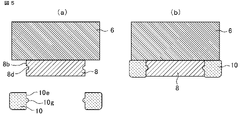
- FIG. FIG. 4 is a cross-sectional view illustrating the shape of a second flexible insulator according to Embodiment 1
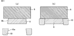
- 8 is another cross-sectional view for explaining the shape of the second flexible insulator according to Embodiment 1
- FIG. 8 is another cross-sectional view for explaining the shape of the second flexible insulator according to Embodiment 1
- FIG. 10 is a diagram showing the configuration of a pressure contact type semiconductor device according to a second embodiment
- FIG. 8 is a cross-sectional view for explaining shapes of a first flexible insulator and a second flexible insulator according to Embodiment 2
- FIG. 10 is a diagram showing the configuration of a pressure contact type semiconductor device according to a third embodiment
- FIG. 10 is a cross-sectional view illustrating shapes of a first flexible insulator and a second flexible insulator according to Embodiment 3;
- FIG. 1 is a diagram showing the configuration of a pressure contact type semiconductor device according to the first embodiment.
- the pressure-contact type semiconductor device is in a state of being pressure-contacted by an external pressure-contact force.
- a first flexible insulator 9 arranged on the base plate electrode 1 to surround the semiconductor chip 4; the base plate electrode 1 and the first flexible insulator 9;
- a frame 3 arranged between the plate electrode 2, an elastic conductor 6 and a current-carrying block 8 which are electrically connected to the semiconductor chip 4 by pressure contact force, and a current-carrying block 8, which are arranged on the elastic conductor 6 and are electrically connected to the elastic conductor 6.
- the current-carrying block 8 is arranged directly below the elastic conductor 6 and has a smaller horizontal cross-sectional area than the elastic conductor 6 . As a result, stepped machining of the current-carrying block 8 is not required.
- the gate wiring extending from the semiconductor chip 4 toward the top plate electrode 2 is the same in the following embodiments, it is omitted.
- the semiconductor chip 4 is, for example, a three-terminal type such as an insulated gate bipolar transistor (IGBT) or a two-terminal type such as a flywheel diode.
- the frame 3 is made of insulating resin such as ceramic, PPS (Poly Phenylene Sulfide), PEEK (Poly Ether Ether Ketone), epoxy, or fluorine resin.
- the first flexible insulator 9 and the second flexible insulator 10 have the flexibility to elastically deform when pressure is applied from the outside, and are made of silicone, epoxy, polyimide, polyamide, or fluorine resin. , and composite resins thereof.
- the first flexible insulator 9 and the second flexible insulator 10 are pre-cured.
- the top plate electrode 2 and the upper surface 6 a of the elastic conductor 6 , the lower surface 6 b of the elastic conductor 6 and the upper surface 8 a of the conducting block 8 , the lower surface 8 f of the conducting block 8 and the upper surface electrode 5 of the semiconductor chip 4 . and the interface between the lower surface 4f of the semiconductor chip 4 and the base plate electrode 1 are electrically and thermally connected to establish contact, and have a spring-like mechanism, for example.
- the term "pressure contact” refers to external mechanical pressure applied between the base plate electrode 1 and the top plate electrode 2 by a pressure contact mechanism or the like.
- the frame 3 is sandwiched between at least one of the base plate electrode 1 and the first flexible insulator 9, and the top plate electrode 2, and is placed between the semiconductor chip 4, the elastic conductor 6, and the current-carrying block 8 during pressure contact. They are held at a constant interval that allows electrical connection between the base plate electrode 1 and the top plate electrode 2 .
- FIG. 2(a) shows the state before pressure contact
- FIG. 2(b) shows the state after pressure contact.
- the first flexible insulator 9 is in contact with the entire height of the side portion 4d of the semiconductor chip 4 and the entire circumference without gaps.
- the outer periphery and upper surface of the first flexible insulator 9 are in contact with the frame 3 without gaps.
- the second flexible insulator 10 is arranged in the space defined by the frame 3, the semiconductor chip 4, the current-carrying block 8, and the elastic conductor 6 in the pressed state, and the entire side surface 8b of the current-carrying block 8 and the lower surface 6b of the elastic conductor 6 without any gap.
- the height 13 of the second flexible insulator is longer than the height of the side surface 8b of the current-carrying block 8, and the thickness 14 of the second flexible insulator is longer than the lower surface 6b of the elastic conductor 6. characterized by By setting the length in this way, when pressure is applied, the semiconductor chip 4, the end of the upper surface electrode 5, the first flexible insulator 9, and the frame 3 are formed as shown in FIG. 2(b). , the current-carrying block 8, and the elastic conductor 6 can be brought into contact with each other without creating a gap.
- the second flexible insulator 10 is in close contact so as to cover the entire circumference of the chip end portion 4b without gaps. Further, the second flexible insulator 10 and the side surface of the frame 3 are in close contact with each other without a gap over the entire circumference. Further, the contact surface between the chip end portion 4b and the first flexible insulator 9 is covered with the bottom surface 10d of the second flexible insulator.
- the electrical connection between the base plate electrode 1 and the top plate electrode 2 is maintained through the semiconductor chip 4, the current-carrying block 8, and the elastic conductor 6, and the first flexibility is maintained.
- the insulator 9 and the second flexible insulator 10 cover the end portion 4b and the side portion 4d of the semiconductor chip 4 without gaps.
- the air discharge path can be blocked only by a simple assembly method that does not use an adhesive, and long-term insulation reliability of the terminal portion 4b of the semiconductor chip 4 is achieved.
- the bottom surface 10d of the second flexible insulator 10 has a slightly convex shape toward the lower side of the paper surface before being press-contacted. It is possible to prevent voids from being caught between the bottom surface 10d of the dielectric insulator 10 and the tip end portion 4b.
- the horizontal cross-sectional area of the current-carrying block 8 is formed to be smaller than the horizontal cross-sectional area of the elastic conductor 6, the current-carrying block does not need to be processed into a stepped structure, and the length of the current-carrying block can be shortened. It is possible to reduce the height of a pressure contact type semiconductor device.
- FIG. 3 is an enlarged cross-sectional view of the semiconductor chip 4.
- the semiconductor chip 4 includes a semiconductor substrate 4a made of a semiconductor material such as Si, SiC, GaN, Ga 2 O 3 , an upper surface electrode 5 for making electrical contact with the upper surface of the semiconductor substrate 4a, and a semiconductor substrate. It is composed of a surface protective material 11 for protecting the surface of 4a. Materials for the surface protective material 11 include TEOS (Tetraethoxysilane), Si 3 N 4 , DLC (Diamond Like Carbon), SIPOS (Semi Insulating POlycrystalline Silicon), parylene, polyimide, polyamide, and polyamideimide.
- the semiconductor chip 4 serves as an energization path that conducts current during ON operation, blocks current during OFF operation, and serves as an insulating layer that maintains a high voltage.
- the applied voltage can range from several kV to several tens of kV. In this case, even if the semiconductor chip 4 has sufficient insulation performance, creeping discharge occurs in the gas layer on the surface of the surface protective material 11 between the upper surface electrode 5 of the semiconductor chip 4 and the semiconductor chip 4. may cause insulation breakdown.
- the elastic conductor 6, the current-carrying block 8, and the second flexible insulator 10 cut off the creeping surface, thereby blocking the air discharge propagation path and improving the air withstand voltage.
- the surface of the surface protective material 11 is reinforced with insulation.
- a bonding process such as an adhesive and a heat curing process are not used, the process is simplified and there is no risk of detachment of the bonded portion due to thermal stress. be.
- the number of semiconductor chips 4 arranged in parallel in the frame is not limited.
- FIGS. 4(a), 5(a), and 6(a) show the current-carrying block 8 and the second flexible insulator 10 before being attached
- FIG. 6(b) shows the state after mounting.
- the side surface 8b of the current-carrying block has a convex portion 8c on at least part of the entire circumference of the block, and the second flexible insulator 10
- the side surface 10 e has a concave portion 10 f shaped to fit the convex portion 8 c of the current-carrying block 8 .
- the side surface 8b of the current-carrying block has a concave portion 8d in at least a part of the entire circumference of the block
- the second flexible insulator 10 has an inner surface 10 e has a convex portion 10 g that fits into the concave portion 8 d of the current-carrying block 8 .
- At least one of the side surfaces 8b of the current-carrying block is formed to widen downward from the top of the paper surface, and the second flexible insulator 10 has a shape that widens upward from the bottom of the paper surface so that the inner side surface 10e thereof fits into the shape of the side surface 8b of the current-carrying block, and as shown in FIG.
- the side surface 8b and the inner side surface 10e are fitted to each other and can be closely attached without any gap. This makes it possible to ensure stability when fixing the second flexible insulator 10 and to facilitate assembly.
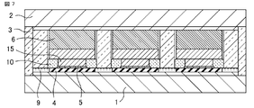
- FIG. 7 is a diagram showing the configuration of a pressure contact type semiconductor device according to the second embodiment.
- the press-contact type semiconductor device is in a press-contact state, a base plate electrode 1 which is a conductor, a semiconductor chip 4 arranged on the base plate electrode 1 and electrically connected to the base plate electrode 1, a base A first flexible insulator 9 arranged on the plate electrode 1 and arranged so as to surround the semiconductor chip 4, between the base plate electrode 1 or the first flexible insulator 9 and the top plate electrode 2 elastic conductor 6 and stepped current-carrying block 15 electrically connected to semiconductor chip 4 by pressing force, and stepped current-carrying block 15, arranged on elastic conductor 6 and electrically connected to elastic conductor 6
- the top plate electrode 2 and the second flexible insulator 10 are in close contact so as to cover the entire chip end portion 4b of the semiconductor chip 4.
- Electrical connection between the base plate electrode 1 and the top plate electrode 2 is made possible via the semiconductor chip 4 , the elastic conductor 6 , and the
- the stepped conducting block 15 is formed such that the horizontal cross-sectional area of the upper portion of the step is approximately the same as that of the elastic conductor 6 and is larger than the horizontal cross-sectional area of the lower portion of the step.
- FIG. 8(a) shows the state before pressure contact
- FIG. 8(b) shows the state after pressure contact
- the second flexible insulator 10 is arranged in a space defined by the frame 3, the semiconductor chip 4 and the stepped current-carrying block 15 in a press-contact state.
- the second flexible insulator 10 is attached to the entire lower side surface 15f of the stepped conducting block 15 and the upper lower surface 15g of the stepped conducting block 15 without gaps.
- the height 13 of the second flexible insulator 10 is longer than the lower side surface 15f of the stepped current-carrying block 15, and the thickness 14 of the second flexible insulator is the upper level of the stepped current-carrying block 15. Longer than the lower surface 15g.
- the same shape as the first to third examples described in the first embodiment can be formed in the combination of the semiconductor chip 4 and the stepped current-carrying block 15. .
- the state of contact between the semiconductor chip 4 and the second flexible insulator 10 during pressure contact is the same as that described with reference to FIG.
- the frame 3 and the stepped current-carrying block 15 can be brought into contact with each other without creating a gap.
- the second flexible insulator 10 is brought into intimate contact so as to cover the entire circumference of the chip end portion 4b without gaps.
- the second flexible insulator 10 and the side surface of the frame 3 are in close contact with each other without a gap over the entire circumference.
- the contact surface between the chip end portion 4b and the first flexible insulator 9 is covered with the bottom surface 10d of the second flexible insulator.
- the electrical connection between the base plate electrode 1 and the top plate electrode 2 is maintained through the semiconductor chip 4, the stepped current-carrying block 15, and the elastic conductor 6, and the first flexible contact is maintained.
- the flexible insulator 9 and the second flexible insulator 10 cover the end portion 4b and the side portion 4d of the semiconductor chip 4 without gaps.
- the air discharge path can be blocked only by a simple assembly method that does not use an adhesive or the like, and the dielectric breakdown voltage is improved. be. Thereby, long-term insulation reliability of the terminal portion 4b of the semiconductor chip 4 is achieved.
- the bottom surface 10d of the second flexible insulator 10 has a slightly convex shape toward the lower side of the paper surface before pressure contact. It is sometimes possible to prevent voids from being caught between the bottom surface 10d of the second flexible insulator 10 and the tip end portion 4b.
- FIG. 9 is a diagram showing the configuration of a pressure contact type semiconductor device according to the third embodiment.
- the press-contact type semiconductor device is in a press-contact state, and includes a base plate electrode 1, a top plate electrode 2, an elastic conductor 6 arranged above the base plate electrode 1, and an elastic conductor 6 arranged above the elastic conductor 6, which are conductors.
- a lower frame 3a provided between the base plate electrode 1 and the top plate electrode 2 so as to surround the elastic conductor 6; , a stepped conducting block 16 disposed on the semiconductor chip 4 and electrically connected to both the top plate electrode 2 and the semiconductor chip 4, the first flexible insulator 9 and the top plate electrode 2
- Upper frame 3b arranged to surround stepped current-carrying block 16, lower frame 3a, first flexible insulator 9, outer frame 3c arranged to surround upper frame 3b, semiconductor chip 4 is composed of a second flexible insulator 10 that adheres so as to cover the entire end portion 4b. Electrical connection between the base plate electrode 1 and the top plate electrode 2 is made possible via the elastic conductor 6 , the semiconductor chip 4 , and the stepped current-carrying block 16 .
- the configuration (materials and shape) is the same as that described in Embodiment 1 except for the configuration of the stepped current-carrying block 16, the configuration of the frame, and the arrangement location of the elastic conductor 6, and detailed description thereof will be omitted.
- the horizontal cross-sectional area of the stepped upper portion is larger than the horizontal cross-sectional area of the stepped lower portion.
- the semiconductor chip 4 has the same material and shape as those shown in the first embodiment.
- the lower frame 3a, the upper frame 3b and the outer frame 3c have the same material as the frame 3 shown in the first embodiment.
- FIG. 10(a) shows the state before pressure contact
- FIG. 10(b) shows the state after pressure contact.
- the second flexible insulator 10 is arranged in a space formed by the upper frame 3b, the semiconductor chip 4, and the stepped current-carrying block 16 in a press-contact state.
- the second flexible insulator 10 is attached to the entire lower side surface 16f of the stepped conducting block 16 and the upper lower surface 16g of the stepped conducting block 16 without gaps.
- the height 13 of the second flexible insulator 10 is longer than the lower side surface 16f of the stepped current-carrying block 16, and the thickness 14 of the second flexible insulator is the upper level of the stepped current-carrying block 16. Longer than the lower surface 16g.
- the same shape as the first to third examples described in the first embodiment can be formed in the combination of the semiconductor chip 4 and the stepped current-carrying block 16. .
- the state of contact between the semiconductor chip 4 and the second flexible insulator 10 during pressure contact is the same as that described with reference to FIG.
- the second flexible insulator 10 is brought into intimate contact so as to cover the entire circumference of the chip end portion 4b without gaps.
- the second flexible insulator 10 and the side surface of the frame 3 are in close contact with each other without a gap over the entire circumference.
- the contact surface between the chip end portion 4b and the first flexible insulator 9 is covered with the bottom surface 10d of the second flexible insulator.
- the electrical connection between the base plate electrode 1 and the top plate electrode 2 is maintained through the elastic conductor 6, the semiconductor chip 4, and the stepped current-carrying block 16, and the first flexible contact is maintained.
- the flexible insulator 9 and the second flexible insulator 10 cover the end portion 4b and the side portion 4d of the semiconductor chip 4 without gaps.
- the air discharge path can be blocked only by a simple assembly method that does not use an adhesive or the like, and the dielectric breakdown voltage is improved. be. Thereby, long-term insulation reliability of the terminal portion 4b of the semiconductor chip 4 is achieved.
- the bottom surface 10d of the second flexible insulator 10 has a slightly convex shape toward the lower side of the paper surface before pressure contact. It is sometimes possible to prevent voids from being caught between the bottom surface 10d of the second flexible insulator 10 and the tip end portion 4b.
Landscapes
- Die Bonding (AREA)
Priority Applications (3)
| Application Number | Priority Date | Filing Date | Title |
|---|---|---|---|
| JP2023526791A JP7580601B2 (ja) | 2021-06-11 | 2021-06-11 | 圧接型半導体装置 |
| PCT/JP2021/022239 WO2022259503A1 (ja) | 2021-06-11 | 2021-06-11 | 圧接型半導体装置 |
| DE112021007808.9T DE112021007808B4 (de) | 2021-06-11 | 2021-06-11 | Halbleitereinrichtung vom druckkontakttyp |
Applications Claiming Priority (1)
| Application Number | Priority Date | Filing Date | Title |
|---|---|---|---|
| PCT/JP2021/022239 WO2022259503A1 (ja) | 2021-06-11 | 2021-06-11 | 圧接型半導体装置 |
Publications (1)
| Publication Number | Publication Date |
|---|---|
| WO2022259503A1 true WO2022259503A1 (ja) | 2022-12-15 |
Family
ID=84425101
Family Applications (1)
| Application Number | Title | Priority Date | Filing Date |
|---|---|---|---|
| PCT/JP2021/022239 Ceased WO2022259503A1 (ja) | 2021-06-11 | 2021-06-11 | 圧接型半導体装置 |
Country Status (3)
| Country | Link |
|---|---|
| JP (1) | JP7580601B2 (https=) |
| DE (1) | DE112021007808B4 (https=) |
| WO (1) | WO2022259503A1 (https=) |
Citations (6)
| Publication number | Priority date | Publication date | Assignee | Title |
|---|---|---|---|---|
| JPH01152668A (ja) * | 1987-12-09 | 1989-06-15 | Fuji Electric Co Ltd | 半導体装置の製造方法 |
| JP2002057260A (ja) * | 2000-08-09 | 2002-02-22 | Fuji Electric Co Ltd | 平型半導体装置 |
| JP2002151646A (ja) * | 2000-11-10 | 2002-05-24 | Toshiba Corp | 圧接型半導体装置 |
| US20020145188A1 (en) * | 1999-09-07 | 2002-10-10 | Hironori Kodama | Flat semiconductor device and power converter employing the same |
| JP2017084850A (ja) * | 2015-10-22 | 2017-05-18 | 日本発條株式会社 | 電力用半導体装置 |
| WO2019116736A1 (ja) * | 2017-12-12 | 2019-06-20 | 三菱電機株式会社 | 圧接型半導体装置及び圧接型半導体装置の製造方法 |
Family Cites Families (3)
| Publication number | Priority date | Publication date | Assignee | Title |
|---|---|---|---|---|
| JP3256636B2 (ja) | 1994-09-15 | 2002-02-12 | 株式会社東芝 | 圧接型半導体装置 |
| US5726466A (en) * | 1995-09-11 | 1998-03-10 | Kabushiki Kaisha Toshiba | Press pack power semiconductor device incorporating a plurality of semiconductor elements |
| JP3684834B2 (ja) * | 1998-04-21 | 2005-08-17 | 三菱電機株式会社 | 圧接型半導体装置 |
-
2021
- 2021-06-11 DE DE112021007808.9T patent/DE112021007808B4/de active Active
- 2021-06-11 WO PCT/JP2021/022239 patent/WO2022259503A1/ja not_active Ceased
- 2021-06-11 JP JP2023526791A patent/JP7580601B2/ja active Active
Patent Citations (6)
| Publication number | Priority date | Publication date | Assignee | Title |
|---|---|---|---|---|
| JPH01152668A (ja) * | 1987-12-09 | 1989-06-15 | Fuji Electric Co Ltd | 半導体装置の製造方法 |
| US20020145188A1 (en) * | 1999-09-07 | 2002-10-10 | Hironori Kodama | Flat semiconductor device and power converter employing the same |
| JP2002057260A (ja) * | 2000-08-09 | 2002-02-22 | Fuji Electric Co Ltd | 平型半導体装置 |
| JP2002151646A (ja) * | 2000-11-10 | 2002-05-24 | Toshiba Corp | 圧接型半導体装置 |
| JP2017084850A (ja) * | 2015-10-22 | 2017-05-18 | 日本発條株式会社 | 電力用半導体装置 |
| WO2019116736A1 (ja) * | 2017-12-12 | 2019-06-20 | 三菱電機株式会社 | 圧接型半導体装置及び圧接型半導体装置の製造方法 |
Also Published As
| Publication number | Publication date |
|---|---|
| DE112021007808T5 (de) | 2024-03-21 |
| JPWO2022259503A1 (https=) | 2022-12-15 |
| DE112021007808B4 (de) | 2025-11-13 |
| JP7580601B2 (ja) | 2024-11-11 |
Similar Documents
| Publication | Publication Date | Title |
|---|---|---|
| US9171773B2 (en) | Semiconductor device | |
| JP6398270B2 (ja) | 半導体装置 | |
| EP1860697A2 (en) | Semiconductor device | |
| JP6676079B2 (ja) | 半導体装置およびその製造方法 | |
| JPH10335579A (ja) | 大電力半導体モジュール装置 | |
| WO2018194153A1 (ja) | 電力用半導体モジュール、電子部品および電力用半導体モジュールの製造方法 | |
| CN113206048B (zh) | 半导体装置及其制造方法 | |
| WO2017082122A1 (ja) | パワーモジュール | |
| JP2012015222A (ja) | 半導体装置 | |
| EP1739740A2 (en) | Power semiconductor | |
| JP7190985B2 (ja) | 半導体装置 | |
| JP2913247B2 (ja) | パワー半導体モジュール及び車両用インバータ装置 | |
| JP3440824B2 (ja) | 半導体装置 | |
| US10601307B1 (en) | Semiconductor device and method for manufacturing the same | |
| CN114078790B (zh) | 功率半导体模块装置及其制造方法 | |
| JPWO2021001927A1 (ja) | 半導体装置、半導体装置の製造方法および電力変換装置 | |
| JP2022144711A (ja) | 半導体装置の製造方法 | |
| CN113363231A (zh) | 半导体装置 | |
| JPH10173098A (ja) | パワー半導体装置およびその製法 | |
| CN104798194A (zh) | 半导体器件 | |
| JP2021028921A (ja) | 圧接型半導体装置及び圧接型半導体装置の製造方法 | |
| WO2022259503A1 (ja) | 圧接型半導体装置 | |
| JP7720918B2 (ja) | 電力用半導体装置および電力用半導体装置の製造方法 | |
| US12512378B2 (en) | Semiconductor module and semiconductor module manufacturing method | |
| JPH06302734A (ja) | 電力用半導体モジュール |
Legal Events
| Date | Code | Title | Description |
|---|---|---|---|
| 121 | Ep: the epo has been informed by wipo that ep was designated in this application |
Ref document number: 21945177 Country of ref document: EP Kind code of ref document: A1 |
|
| WWE | Wipo information: entry into national phase |
Ref document number: 2023526791 Country of ref document: JP |
|
| WWE | Wipo information: entry into national phase |
Ref document number: 112021007808 Country of ref document: DE |
|
| 122 | Ep: pct application non-entry in european phase |
Ref document number: 21945177 Country of ref document: EP Kind code of ref document: A1 |
|
| WWG | Wipo information: grant in national office |
Ref document number: 112021007808 Country of ref document: DE |