WO2022239167A1 - 金属補強板付きプリント配線板の製造方法、部材セット、及び金属補強板付きプリント配線板 - Google Patents
金属補強板付きプリント配線板の製造方法、部材セット、及び金属補強板付きプリント配線板 Download PDFInfo
- Publication number
- WO2022239167A1 WO2022239167A1 PCT/JP2021/018129 JP2021018129W WO2022239167A1 WO 2022239167 A1 WO2022239167 A1 WO 2022239167A1 JP 2021018129 W JP2021018129 W JP 2021018129W WO 2022239167 A1 WO2022239167 A1 WO 2022239167A1
- Authority
- WO
- WIPO (PCT)
- Prior art keywords
- conductive adhesive
- reinforcing plate
- metal reinforcing
- wiring board
- mpa
- Prior art date
- Legal status (The legal status is an assumption and is not a legal conclusion. Google has not performed a legal analysis and makes no representation as to the accuracy of the status listed.)
- Ceased
Links
Images








Classifications
-
- H—ELECTRICITY
- H05—ELECTRIC TECHNIQUES NOT OTHERWISE PROVIDED FOR
- H05K—PRINTED CIRCUITS; CASINGS OR CONSTRUCTIONAL DETAILS OF ELECTRIC APPARATUS; MANUFACTURE OF ASSEMBLAGES OF ELECTRICAL COMPONENTS
- H05K3/00—Apparatus or processes for manufacturing printed circuits
- H05K3/0058—Laminating printed circuit boards onto other substrates, e.g. metallic substrates
-
- C—CHEMISTRY; METALLURGY
- C09—DYES; PAINTS; POLISHES; NATURAL RESINS; ADHESIVES; COMPOSITIONS NOT OTHERWISE PROVIDED FOR; APPLICATIONS OF MATERIALS NOT OTHERWISE PROVIDED FOR
- C09J—ADHESIVES; NON-MECHANICAL ASPECTS OF ADHESIVE PROCESSES IN GENERAL; ADHESIVE PROCESSES NOT PROVIDED FOR ELSEWHERE; USE OF MATERIALS AS ADHESIVES
- C09J9/00—Adhesives characterised by their physical nature or the effects produced, e.g. glue sticks
- C09J9/02—Electrically-conducting adhesives
-
- H—ELECTRICITY
- H05—ELECTRIC TECHNIQUES NOT OTHERWISE PROVIDED FOR
- H05K—PRINTED CIRCUITS; CASINGS OR CONSTRUCTIONAL DETAILS OF ELECTRIC APPARATUS; MANUFACTURE OF ASSEMBLAGES OF ELECTRICAL COMPONENTS
- H05K1/00—Printed circuits
- H05K1/02—Details
-
- H—ELECTRICITY
- H05—ELECTRIC TECHNIQUES NOT OTHERWISE PROVIDED FOR
- H05K—PRINTED CIRCUITS; CASINGS OR CONSTRUCTIONAL DETAILS OF ELECTRIC APPARATUS; MANUFACTURE OF ASSEMBLAGES OF ELECTRICAL COMPONENTS
- H05K1/00—Printed circuits
- H05K1/02—Details
- H05K1/0213—Electrical arrangements not otherwise provided for
- H05K1/0216—Reduction of cross-talk, noise or electromagnetic interference
- H05K1/0218—Reduction of cross-talk, noise or electromagnetic interference by printed shielding conductors, ground planes or power plane
-
- H—ELECTRICITY
- H05—ELECTRIC TECHNIQUES NOT OTHERWISE PROVIDED FOR
- H05K—PRINTED CIRCUITS; CASINGS OR CONSTRUCTIONAL DETAILS OF ELECTRIC APPARATUS; MANUFACTURE OF ASSEMBLAGES OF ELECTRICAL COMPONENTS
- H05K1/00—Printed circuits
- H05K1/02—Details
- H05K1/0213—Electrical arrangements not otherwise provided for
- H05K1/0254—High voltage adaptations; Electrical insulation details; Overvoltage or electrostatic discharge protection ; Arrangements for regulating voltages or for using plural voltages
- H05K1/0256—Electrical insulation details, e.g. around high voltage areas
-
- H—ELECTRICITY
- H05—ELECTRIC TECHNIQUES NOT OTHERWISE PROVIDED FOR
- H05K—PRINTED CIRCUITS; CASINGS OR CONSTRUCTIONAL DETAILS OF ELECTRIC APPARATUS; MANUFACTURE OF ASSEMBLAGES OF ELECTRICAL COMPONENTS
- H05K3/00—Apparatus or processes for manufacturing printed circuits
- H05K3/30—Assembling printed circuits with electric components, e.g. with resistors
- H05K3/32—Assembling printed circuits with electric components, e.g. with resistors electrically connecting electric components or wires to printed circuits
-
- H—ELECTRICITY
- H05—ELECTRIC TECHNIQUES NOT OTHERWISE PROVIDED FOR
- H05K—PRINTED CIRCUITS; CASINGS OR CONSTRUCTIONAL DETAILS OF ELECTRIC APPARATUS; MANUFACTURE OF ASSEMBLAGES OF ELECTRICAL COMPONENTS
- H05K9/00—Screening of apparatus or components against electric or magnetic fields
-
- H—ELECTRICITY
- H05—ELECTRIC TECHNIQUES NOT OTHERWISE PROVIDED FOR
- H05K—PRINTED CIRCUITS; CASINGS OR CONSTRUCTIONAL DETAILS OF ELECTRIC APPARATUS; MANUFACTURE OF ASSEMBLAGES OF ELECTRICAL COMPONENTS
- H05K2203/00—Indexing scheme relating to apparatus or processes for manufacturing printed circuits covered by H05K3/00
- H05K2203/11—Treatments characterised by their effect, e.g. heating, cooling, roughening
Definitions
- the present invention relates to a method for manufacturing a printed wiring board with a metal reinforcing plate, a member set used in the manufacturing method, and a printed wiring board with a metal reinforcing plate.
- FPC flexible printed wiring boards
- Patent Document 1 discloses an FPC in which a conductive metal reinforcing plate and a ground circuit are connected with a conductive adhesive. Specifically, a conductive adhesive sheet is used to attach a metal reinforcing plate made of stainless steel or the like to the FPC, thereby electrically connecting the metal reinforcing plate to the ground circuit. With such a configuration, it is possible to obtain an FPC with good electromagnetic wave shielding properties, and to stably transmit circuit signals.
- Patent Literature 2 discloses a technique related to a conductive adhesive containing a thermosetting resin and a conductive filler.
- the conductive adhesive When attaching a metal reinforcing plate to an FPC, the conductive adhesive is required to have embedding properties in the opening formed in the insulating protective film of the FPC. Specifically, when a set of members arranged in the order metal reinforcing plate/conductive adhesive/FPC is hot-pressed at a predetermined press temperature (for example, 170° C.), the softening of the conductive adhesive is insufficient. , there is a problem that the fillability of the conductive adhesive into the opening deteriorates. In particular, when the opening is small, the filling property is remarkably deteriorated, resulting in poor conduction. Therefore, it is necessary to soften the conductive adhesive at the pressing temperature (eg 170°C). On the other hand, when the conductive adhesive oozes out from between the metal reinforcing plate and the FPC due to the press pressure in the pressing process, it causes problems such as poor appearance and short circuit.
- a predetermined press temperature for example, 170° C.
- the conductive adhesive will exude excessively from between the metal reinforcing plate and the FPC, causing poor appearance and short circuits.
- an object of the present invention is to provide a method for manufacturing a printed wiring board with a metal reinforcing plate, which has good fillability of a conductive adhesive in openings and can prevent appearance defects and short circuits, and the printed wiring board. and a printed wiring board with a metal reinforcing plate for use in the manufacturing method of the above.
- a method for manufacturing a printed wiring board with a metal reinforcing plate according to one aspect of the present invention is a printed wiring board in which a circuit pattern including a ground circuit and an insulating protective film that insulates and protects the circuit pattern and has an opening are formed.
- the member set is hot-pressed to bond the ground circuit and the metal reinforcing plate with the conductive adhesive through the opening provided in the insulating protective film, and the ground circuit and the metal reinforcing plate are bonded together.
- a member set according to an aspect of the present invention includes a printed wiring board having a circuit pattern including a ground circuit, and an insulating protective film that insulates and protects the circuit pattern and has an opening penetrating to the ground circuit.
- a metal reinforcing plate joined to the printed wiring board by hot pressing a member set used for manufacturing a printed wiring board with a metal reinforcing plate, It contains a binder resin that is softened by heat and a conductive filler, is filled into the opening by the heat press, electrically connects the ground circuit and the metal reinforcing plate, and connects the metal reinforcing plate to the printed wiring.
- a conductive adhesive to be bonded to the plate, the metal reinforcing plate, and a cushioning material that softens during the hot press and flows into the side surface of the conductive adhesive and the metal reinforcing plate are arranged in this order. .
- INDUSTRIAL APPLICABILITY it is used in a method for manufacturing a printed wiring board with a metal reinforcing plate, which has a good filling property of a conductive adhesive in an opening and can prevent appearance defects and short circuits, and a method for manufacturing the printed wiring board.
- a printed wiring board with a member set and a metal reinforcing plate can be provided.
- FIG. 10 is a diagram for explaining a member set preparation step [1] according to the embodiment;
- FIG. 10 is a diagram for explaining a member set preparation step [2] according to the embodiment;
- FIG. 10 is a diagram for explaining a member set preparation step [3] according to the embodiment;
- FIG. 2 is a diagram for explaining a method (step [1]) for manufacturing a printed wiring board with a metal reinforcing plate according to the embodiment;
- FIG. 4 is a diagram for explaining the method of manufacturing a printed wiring board with a metal reinforcing plate according to the embodiment (step [2]);
- FIG. 10 is a diagram for explaining a member set preparation step [1] according to the embodiment
- FIG. 10 is a diagram for explaining a member set preparation step [2] according to the embodiment
- FIG. 10 is a diagram for explaining a member set preparation step [3] according to the embodiment
- FIG. 2 is a diagram for explaining a method (step [1]) for manufacturing a printed wiring board with
- FIG. 4 is a diagram for explaining the method (step [3]) for manufacturing a printed wiring board with a metal reinforcing plate according to the embodiment; 1 is a cross-sectional view of a printed wiring board with a metal reinforcing plate according to an embodiment; FIG. It is a sectional view of a member set concerning an embodiment. FIG. 11 is a cross-sectional view of a member set according to another embodiment; FIG. 5 is a cross-sectional view of a printed wiring board with a metal reinforcing plate according to a comparative example, for explaining poor embedding properties of a conductive adhesive into an opening.
- FIG. 5 is a cross-sectional view of a printed wiring board with a metal reinforcing plate according to a comparative example, for explaining a defect in seeping of a conductive adhesive
- FIG. 10 is a plan view of a printed wiring board according to a comparative example for explaining a leaking defect of a conductive adhesive
- FIG. 4 is a schematic plan view of a printed wiring board with a metal reinforcing plate according to a comparative example, for explaining the bleeding failure of the conductive adhesive;
- a sheet in this specification includes not only a sheet defined in JIS but also a film. For clarity of explanation, the following description and drawings have been simplified where appropriate. Unless otherwise noted, the various components appearing in this specification may be used singly or in combination of two or more. In this specification, “printed wiring board” may be abbreviated as “wiring board”. Hereinafter, examples of embodiments of the present invention will be described.
- FIGS. 1A to 2C show a manufacturing process for attaching a metal reinforcing plate to a printed wiring board using a conductive adhesive.
- conductive adhesive refers to a conductive adhesive before heat curing
- conductive adhesive layer refers to a layer obtained by heat curing a conductive adhesive (that is, , conductive adhesive after thermosetting), and both are given the same reference numerals.
- a conductive adhesive sheet 13 having a conductive adhesive 12 formed on a peelable film 11 and a metal reinforcing plate 14 are prepared.
- the conductive adhesive 12 side of the conductive adhesive sheet 13 is attached to the metal reinforcing plate 14, and the conductive adhesive sheet 13 is temporarily attached to the metal reinforcing plate 14. do.
- the temperature at which the conductive adhesive sheet 13 is temporarily attached to the metal reinforcing plate 14 can be, for example, 110.degree. C. to 150.degree. C., preferably 130.degree.
- the conductive adhesive 12 is in a semi-cured state.
- the peelable film 11 is peeled off to expose the surface of the conductive adhesive 12 opposite to the metal reinforcing plate 14 .
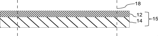
- the preliminary laminate 15 of the conductive adhesive 12 and the metal reinforcing plate 14 is cut to a predetermined size (the cutting line is indicated by reference numeral 18).
- the cutting of the pre-laminate 15 can be performed, for example, using a stamping process.
- the peelable film 11 may be peeled off after the cutting step.
- a printed wiring board is prepared on which a circuit pattern including a ground circuit and an insulating protective film that insulates and protects the circuit pattern and has an opening is formed. Then, above the insulating protective film of the printed wiring board, a member set having, in this order, a conductive adhesive containing a binder resin and a conductive filler that are softened by heat, a metal reinforcing plate, and a cushioning material is mounted on the wiring. In this step, the plate and the conductive adhesive are arranged so as to face each other.
- the member set of the present invention is used when (i) the layers of the conductive adhesive/metal reinforcing plate/cushion material are integrated and then used, and (ii) the respective layers are arranged in order above the printed wiring board. (iii) when a cushioning material is arranged in a preliminary laminate in which a conductive adhesive and a metal reinforcing plate are integrated; This includes the case where a preliminary laminate is arranged and used. That is, in this member set, the conductive adhesive, the metal reinforcing plate, and the cushioning material may be arranged in this order at the time of hot pressing. And the metal reinforcing plate and the cushion member may be independently non-integral or integral.
- integrated means not only being stacked but also stuck (laminated), and "non-integrated” means not stuck but stacked.
- at least the member set of this agent set is integrated.
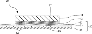
- Wiring board 20 has a structure in which base material 21 on the lower side and insulating film 22 on the upper side are adhered with insulating adhesive 23 .
- a signal circuit 24 and a ground circuit 25 are formed on the substrate 21.
- Above the ground circuit 25 are an insulating film 22 and an opening (through hole) 27 provided in an insulating adhesive 23. are placed. That is, part of the ground circuit 25 formed on the base material 21 is exposed through the opening 27 .
- Member set 17 is arranged above opening 27 of wiring board 20 .
- the insulating film 22 and the insulating adhesive 23 function as an insulating protective film.
- Step [2]> the member set is hot-pressed, the ground circuit and the metal reinforcing plate are bonded with a conductive adhesive through the opening provided in the insulating protective film of the printed wiring board, and the ground This is the step of electrically connecting the circuit and the metal reinforcing plate.
- the laminate of member set 17/wiring board 20 is hot-pressed (heated/heated) at a predetermined temperature (for example, 150 to 190° C., preferably 170° C.). pressure).
- a predetermined temperature for example, 150 to 190° C., preferably 170° C.
- the conductive adhesive 12 is softened and embedded in the openings 27 formed in the insulating film 22 and the insulating adhesive 23 .
- the conductive adhesive 12 contacts the ground circuit 25 exposed through the opening 27 .
- the conductive adhesive 12 is cured to bond the metal reinforcing plate 14 and the wiring board 20 together, and electrically connect the ground circuit 25 and the metal reinforcing plate 14 .
- the cushioning material 16 is fluidized by heat and pressure, flows into the side surfaces of the metal reinforcing plate 14 and the conductive adhesive 12, and prevents the conductive adhesive 12 from seeping out. That is, the cushion material 16 flows to the side surface of the conductive adhesive 12 before the conductive adhesive 12 seeps out from the metal reinforcing plate during hot pressing, and prevents the seepage. In this state, the cushion material 16 requires hardness (viscoelasticity) to suppress the exudation of the conductive adhesive 12 .
- the pressure during hot pressing is preferably about 3 to 30 kg/cm 2 .
- a flat pressing machine or a roll pressing machine can be used for the hot press.
- the time for hot pressing is not particularly limited as long as the member set of cushion material 16/metal reinforcing plate 14/conductive adhesive 12/wiring board 20 is sufficiently adhered, but usually from 1 minute to. It takes about 1 hour. If the hot press time is short, it is preferable to heat the conductive adhesive 12 in an oven at 150 to 190° C. for 30 minutes to 3 hours after the hot press to fully cure the conductive adhesive 12 .
- Step [3] is a step of peeling off the cushion material of the member set. After the hot pressing, as shown in FIG. 2C, the cushioning material 16 whose fluidity has disappeared due to the decrease in temperature is peeled off by a suction peeling device or manually. As a result, as shown in FIG. 3, the metal reinforcing plate 14 and the ground circuit 25 of the wiring board 20 are electrically connected via the conductive adhesive layer 12, thereby forming a printed wiring with a metal reinforcing plate having electromagnetic wave shielding properties.
- a plate 30 can be manufactured.
- a member set according to the present embodiment is used in the above-described method for manufacturing a printed wiring board with a metal reinforcing plate, and is arranged in the order of a cushion material, a metal reinforcing plate, and a conductive adhesive. As shown in FIG. 4A, each member may have substantially the same size in plan view. In addition, as shown in FIG. 4B , a mode in which a protruding region of the cushion material on which the metal reinforcing plate and the conductive adhesive are not superimposed is provided outside the outer edge of the metal reinforcing plate and the conductive adhesive in a plan view. good too.
- the size of the cushioning material in plan view may be larger than that of the conductive adhesive and the metal reinforcing plate, and the cushioning material may have a region that protrudes from the metal reinforcing plate or the like in plan view.
- the storage elastic modulus of the cushion material is 10 MPa or more and 100 MPa or less at 170 ° C.
- the storage elastic modulus of the conductive adhesive is 170 ° C. is 2 MPa or more and 50 MPa or less
- the storage elastic modulus of the cushion material is preferably higher than that of the conductive adhesive.
- the member set After forming the preliminary laminate 15 composed of the metal reinforcing plate 14 and the conductive adhesive 12 as described above, the member set includes the step of stacking the cushioning material, or the conductive adhesive/metal reinforcement in advance before placing on the wiring board.
- a member set (laminate) in which the plate/cushion material is integrated may be formed.
- a member set that satisfies any one of the following conditions (I) to (III) is preferable from the viewpoint of having excellent embedding properties in openings and more effectively exuding the conductive adhesive.
- the storage modulus of the conductive adhesive at 170° C. is 5.5 MPa or more and 50 MPa or less, and the storage modulus of the cushioning material at 170° C. is 10 MPa or more and 100 MPa or less, and the storage modulus of the conductive adhesive is A component set with a higher cushioning material.
- the storage modulus of the conductive adhesive at 170°C is 2 MPa or more and 50 MPa or less, and the storage modulus of the cushioning material at 170°C is 10 MPa or more and 100 MPa or less, and the storage modulus is higher than that of the conductive adhesive.
- the storage modulus of the conductive adhesive at 170° C. is 2 MPa or more and 50 MPa or less, and the storage modulus of the cushioning material at 170° C. is 10 MPa or more and 100 MPa or less, and the storage modulus is higher than that of the conductive adhesive.
- a member set in which the material is high and the thickness ratio between the metal reinforcing plate and the cushioning material is 1.5 to 2.
- thickness ratio between the metal reinforcing plate and the cushioning material is 1.5 to 2.
- the cushion material uniformly transmits the press pressure of the hot press to the metal reinforcing plate and the conductive adhesive, flows during the hot press, and has a role of suppressing the seepage of the conductive adhesive.
- the storage elastic modulus of the cushioning material at 170°C is preferably 10 MPa or more and 100 MPa or less, more preferably 12 MPa or more and 90 MPa or less, and even more preferably 15 MPa or more and 70 MPa or less.
- the storage elastic modulus of the cushioning material exceeds 100 MPa, as shown in FIG. 4B, the cushioning material cannot disperse the press pressure, and the conductive adhesive 12 is strongly applied to the pressure, so that it softens and tends to seep out.
- the storage elastic modulus is less than 10 MPa, the hardness of the cushioning material is insufficient, and it becomes difficult to suppress exudation due to softening of the conductive adhesive.
- the storage elastic modulus of the cushioning material according to this embodiment can be measured as follows. That is, using a dynamic viscoelasticity measuring device, the storage elastic modulus (E′), loss elastic modulus (E′′), and loss tangent (tan ⁇ ) changes in the temperature range of 25 to 200 ° C. of the cushion material are measured. It can be obtained by extracting the storage elastic modulus (E′) in .
- the melt flow rate (MFR) of the cushioning material is preferably 0.002 g/10 min or more and 17 g/10 min or less, more preferably 0.01 g/10 min or more and 4.0 g/10 min or less.
- MFR melt flow rate
- the cushioning material reaches the side surface and effectively exhibits the effect of suppressing oozing out.
- the embedding of the conductive adhesive 12 is improved by suppressing excessive flow and uniformly transmitting the press pressure.
- the cushion material can be formed from a thermoplastic resin composition containing a thermoplastic resin.
- the thermoplastic resin composition may contain a plasticizer, a thermosetting agent, an inorganic filler, etc. in addition to the thermoplastic resin.
- thermoplastic resins include polyolefin resins, acid-modified polyolefin resins grafted with acid, copolymer resins of polyolefins and unsaturated esters, vinyl resins, styrene/acrylic resins, diene resins, cellulose resins, Polyamide resins, polyurethane resins, polyester resins, polycarbonate resins, polyimide resins, fluorine resins, and the like can be used. Among these, polyolefin resins, acid-modified polyolefin resins grafted with acid, copolymer resins of polyolefins and unsaturated esters, and vinyl resins are preferred.
- the thermoplastic resins may be used singly or as a mixture of two or more at any ratio as required.
- Polyolefin-based resins are preferably homopolymers or copolymers of ethylene, propylene, ⁇ -olefin compounds, and the like. Specific examples include low-density polyethylene, ultra-low-density polyethylene, linear low-density polyethylene, high-density polyethylene, polypropylene homopolymer, polypropylene copolymer, and the like. Among these, polyethylene resin and polypropylene resin are preferred, and polyethylene resin is more preferred.
- the acid-modified polyolefin resin is preferably a polyolefin resin grafted with maleic acid, acrylic acid, methacrylic acid, itaconic acid, or the like. Among these, maleic acid-modified polyolefin resins are preferred.
- Examples of unsaturated esters in copolymer resins of polyolefins and unsaturated esters include methyl acrylate, ethyl acrylate, isobutyl acrylate, n-butyl acrylate, isooctyl acrylate, methyl methacrylate, isobutyl methacrylate, dimethyl maleate, diethyl maleate and glycidyl methacrylate, and the like.
- an ethylene-glycidyl methacrylate copolymer resin composed of ethylene as a polyolefin and glycidyl methacrylate as an unsaturated ester is preferred.
- the vinyl-based resin is preferably a polymer obtained by polymerization of a vinyl ester such as vinyl acetate, or a copolymer of a vinyl ester and an olefin compound such as ethylene.
- a vinyl ester such as vinyl acetate
- a copolymer of a vinyl ester and an olefin compound such as ethylene.
- Specific examples include ethylene-vinyl acetate copolymer, ethylene-vinyl propionate copolymer, partially saponified polyvinyl alcohol, and the like. Among these, ethylene-vinyl acetate copolymers are preferred.
- the styrene-acrylic resin is preferably a homopolymer or copolymer composed of styrene, (meth)acrylonitrile, acrylamides, maleimides, and the like. Specific examples include syndiotactic polystyrene, polyacrylonitrile, and acrylic copolymers.
- the diene-based resin is preferably a homopolymer or copolymer of a conjugated diene compound such as butadiene or isoprene, and a hydrogenated product of these homopolymers or copolymers.
- a conjugated diene compound such as butadiene or isoprene
- a hydrogenated product of these homopolymers or copolymers e.g., styrene-butadiene rubber, styrene-isoprene block copolymer, styrene-ethylene/butylene-styrene block copolymer, styrene-ethylene/propylene-styrene block copolymer, styrene-isoprene-styrene block copolymer, styrene-butylene/butadiene- Examples include styrene block copolymers, mixtures of styrene-ethylene/buty
- Cellulose-based resin is preferably cellulose acetate butyrate resin.
- Polycarbonate resin is preferably bisphenol A polycarbonate.
- Polyimide-based resins are preferably thermoplastic polyimides, polyamide-imide resins, and polyamic acid-type polyimide resins.
- the cushion material may include a release layer in addition to the cushioning member.
- a release layer it is preferable to form a layer made of polypropylene, polymethylpentene, cyclic olefin polymer, silicone, or fluororesin. Among these, more preferable are polypropylene, polymethylpentene, silicone and fluororesin.
- a form in which a release agent such as alkyd or silicone is coated is also preferable.
- the thickness of the release layer is preferably 0.001-70 ⁇ m, more preferably 0.01-50 ⁇ m.
- CR1012 "CR1012MT4", “CR1040”, “CR2031MT4", etc. manufactured by Mitsui Tocello can be used as commercially available cushioning materials.
- These commercially available cushioning materials have a layered structure in which both sides of the cushioning material are sandwiched between polymethylpentene as release layers, and the integral structure of these is called a cushioning material in the present application.
- the thickness of the cushion material is preferably 50-300 ⁇ m, more preferably 75-250 ⁇ m, and even more preferably 100-200 ⁇ m. By setting the thickness to 50 to 300 ⁇ m, the exudation property can be improved. In addition, the said thickness is a value including a mold release layer, when it has a mold release layer.
- Metal reinforcing plates include conductive metals such as gold, silver, copper, iron and stainless steel. Among these, stainless steel is preferable in terms of strength, cost and chemical stability as a reinforcing plate.
- the thickness of the metal reinforcing plate is preferably 50-500 ⁇ m, more preferably 60-400 ⁇ m, even more preferably 75-300 ⁇ m.
- the thickness of the metal reinforcing plate is preferably 50-500 ⁇ m, more preferably 60-400 ⁇ m, even more preferably 75-300 ⁇ m.
- the metal reinforcing plate preferably has a plated layer formed on its surface in order to suppress an increase in resistance value due to non-conductivity of the surface.
- the plating layer is preferably gold, silver, nickel, or phosphorous-containing nickel plating.
- the plating method is preferably electrolytic plating or electroless plating.
- the thickness of the plated layer is approximately 0.1 to 5 ⁇ m, preferably 0.2 to 4 ⁇ m. Incidentally, the thickness of the metal reinforcing plate is a value including the plated layer when it has a plated layer. From the viewpoint of cost reduction, it is preferable to avoid plating.
- the thickness ratio between the metal reinforcing plate and the cushioning material is preferably 2 or less. It is more preferably 1.7 or less, even more preferably 1.3 or less.
- the lower limit is preferably 0.1 or more, more preferably 0.5 or more.
- the conductive adhesive according to the present embodiment preferably contains at least a binder resin softened by heat and a conductive filler, and preferably has the following properties.
- the storage elastic modulus of the conductive adhesive at 170° C. may be 2 MPa or more and 50 MPa or less, preferably 4 MPa or more and 25 MPa or less, more preferably 7 MPa or more and 15 MPa or less.
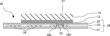
- the conductive adhesive 12 is sufficiently softened during hot pressing (see step [1] in FIG. 2A to step [3] in FIG. 2C). It is possible to improve the fillability of the conductive adhesive 12 into the opening. Therefore, the formation of a gap 29b (see FIG.
- Methods for increasing the storage elastic modulus at 170° C. to 2 MPa or more include, for example, increasing the weight-average molecular weight Mw of the binder resin, making the binder resin a skeleton having many aromatic rings to increase rigidity, and conducting fillers and inorganic fillers.
- the binder resin is a thermosetting resin
- methods such as increasing the cross-linking density with the curing agent in the B stage can be used.
- Techniques for making the storage elastic modulus at 170° C. to 50 MPa or less include, for example, lowering the weight average molecular weight Mw of the binder resin, reducing the rigidity of the binder resin by reducing aromatic rings, adding conductive fillers, inorganic fillers, and the like. Techniques include reducing the amount of filler component added, and when the binder resin is a thermosetting resin, lowering the crosslink density with the curing agent in the B stage, which is in the semi-cured state.
- the storage elastic modulus of the conductive adhesive at 170° C. to the range described above, a conductive adhesive having good filling properties in openings during manufacturing of a printed wiring board with a metal reinforcing plate can be obtained. and a printed wiring board with a metal reinforcing plate.
- the storage elastic modulus of the conductive adhesive according to this embodiment can be obtained by the same method as for the cushion material.
- the storage elastic modulus of the cushioning material is preferably higher than that of the conductive adhesive.
- the difference in storage elastic modulus at 170° C. between the cushion material and the conductive adhesive is preferably 4 to 100 MPa, more preferably 10 to 87 MPa.
- the loss tangent (tan ⁇ ) of the conductive adhesive at 170° C. is preferably 0.05 or more and 0.4 or less, more preferably 0.15 or more and 0.35 or less, and 0.20 or more and 0.20 or more. 3 or less is more preferable.
- the loss tangent (tan ⁇ ) of the conductive adhesive at 170° C. is preferably 0.05 or more and 0.4 or less, more preferably 0.15 or more and 0.35 or less, and 0.20 or more and 0.20 or more. 3 or less is more preferable.
- Techniques for making the loss tangent at 170° C. 0.05 or more include, for example, lowering the weight average molecular weight Mw of the binder resin, lowering the acid value of the binder resin, lowering the glass transition temperature (Tg) of the binder resin, and and adding a curing agent that is liquid at room temperature.
- Methods for making the loss tangent at 170° C. 0.40 or less include, for example, increasing the weight-average molecular weight Mw of the binder resin, increasing the acid value of the binder resin, increasing the Tg of the binder resin, and adding a solid at room temperature. For example, a curing agent is added.
- the loss tangent (tan ⁇ ) of the conductive adhesive according to the present embodiment is the storage elastic modulus (E' ), loss modulus (E′′), and loss tangent (tan ⁇ ), and extract the loss tangent (tan ⁇ ) at each temperature.
- the conductive adhesive of the present embodiment can be determined using the peak temperature in the temperature-loss tangent (tan ⁇ ) curve obtained by viscoelasticity measurement.
- the conductive adhesive of the present invention preferably has first and second glass transition temperatures, with the low temperature peak defined as the first glass transition temperature and the high temperature peak defined as the second glass transition temperature.
- the first glass transition temperature is 10° C. or higher and 45° C. or lower
- the second glass transition temperature is 70° C. or higher and 140° C. or lower. More preferably, the first glass transition temperature is 25° C. or higher and 40° C. or lower
- the second glass transition temperature is 75° C. or higher and 110° C. or lower.
- the first glass transition temperature is 27° C. or higher and 36° C. or lower
- the second glass transition temperature is 78° C. or higher and 95° C. or lower.
- Techniques for setting the first glass transition temperature to 10° C. or higher and 45° C. or lower include, for example, a method of controlling the Tg of the binder resin, and when the binder resin is a thermosetting resin, the cross-linking density with the curing agent is adjusted. There are methods of control. In order to set the second glass transition temperature to 70° C. or higher and 140° C. or lower, the same method as described above can be used for adjustment.
- the thickness of the conductive adhesive is preferably 15-70 ⁇ m, more preferably 20-65 ⁇ m. By setting the thickness to 15 ⁇ m or more, it is possible to improve the embedding property in a small opening via. By setting the thickness to 70 ⁇ m or less, the bleeding property can be suppressed.
- the thickness of the conductive adhesive can be measured by a contact-type film thickness meter, cross-sectional observation, or the like.
- the conductive adhesive that constitutes the member set can be produced, for example, from a conductive adhesive sheet using a conductive resin composition and forming a conductive adhesive on a peelable film.
- the conductive adhesive according to the present embodiment is preferably formed from a conductive resin composition containing a binder resin softened by heat and conductive fine particles.
- the binder resin softened by heat is not particularly limited as long as it does not deviate from the gist of the present invention, but thermosetting resins are preferred.
- Thermoplastic resins are preferred for applications in which there is no heating process such as a reflow process in the post-process.
- a self-crosslinking type and a curing agent reaction type can be used for the thermosetting resin.
- a thermosetting resin having a reactive functional group capable of reacting with a curing agent is suitable as the curing agent reaction type binder resin.
- thermosetting resin is a resin having a plurality of functional groups that can be used for a cross-linking reaction by heating.
- functional groups include hydroxyl groups, phenolic hydroxyl groups, carboxyl groups, amino groups, epoxy groups, oxetanyl groups, oxazoline groups, oxazine groups, aziridine groups, thiol groups, isocyanate groups, blocked isocyanate groups, silanol groups, and the like.
- Thermosetting resins having the above functional groups include, for example, acrylic resins, maleic acid resins, polybutadiene resins, polyester resins, condensation type polyester resins, addition type polyester resins, melamine resins, polyurethane resins, polyurethane urea resins, and epoxy resins. , oxetane resins, phenoxy resins, polyimide resins, polyamide resins, polyamideimide resins, phenolic resins, alkyd resins, amino resins, polylactic acid resins, oxazoline resins, benzoxazine resins, silicone resins, and fluorine resins.
- polyurethane resins, polyurethane urea resins, epoxy resins, addition type polyester resins, polyimide resins, polyamide resins, and polyamideimide resins are preferred.
- the weight average molecular weight (Mw) of the thermosetting resin is preferably 50,000 to 200,000, more preferably 70,000 to 130,000.
- Mw weight average molecular weight
- the glass transition temperature (Tg) of the thermosetting resin is preferably -20°C to 20°C, more preferably -7°C to 150°C. By setting the glass transition temperature within the above range, the storage elastic modulus of the conductive adhesive at 25°C can be made suitable.
- the acid value of the thermosetting resin is preferably 1-40 mgKOH/g, more preferably 4-15 mgKOH/g, and even more preferably 6-13 mgKOH/g.
- the curing agent can be arbitrarily selected according to the type of thermosetting resin. As a curing agent, it functions to make a semi-cured state when forming a conductive adhesive by a cross-linking reaction, and does not completely cure when forming a conductive adhesive sheet, and is hot-pressed to a wiring board or a metal reinforcing plate. A curing agent that cures at the time can also be appropriately selected. Curing agents include epoxy compounds, isocyanate curing agents, amine curing agents, aziridine curing agents, and imidazole curing agents.
- epoxy compound a glycidyl ether type epoxy compound, a glycidyl amine type epoxy compound, a glycidyl ester type epoxy compound, a cycloaliphatic (alicyclic type) epoxy compound, and the like are preferable.
- Examples of the glycidyl ether type epoxy compounds include bisphenol A type epoxy compounds, bisphenol F type epoxy compounds, bisphenol S type epoxy compounds, bisphenol AD type epoxy compounds, cresol novolak type epoxy compounds, phenol novolak type epoxy compounds, ⁇ -naphthol novolak type.
- Epoxy compounds, bisphenol A type novolak type epoxy compounds, dicyclopentadiene type epoxy compounds, tetrabromobisphenol A type epoxy compounds, brominated phenol novolac type epoxy compounds, tris(glycidyloxyphenyl)methane, tetrakis(glycidyloxyphenyl)ethane, etc. is mentioned.
- glycidylamine-type epoxy compounds examples include tetraglycidyldiaminodiphenylmethane, triglycidyl para-aminophenol, triglycidylmethaminophenol, tetraglycidylmethaxylylenediamine, and the like.
- Examples of the glycidyl ester type epoxy compound include diglycidyl phthalate, diglycidyl hexahydrophthalate, and diglycidyl tetrahydrophthalate.
- cycloaliphatic (alicyclic) epoxy compounds examples include epoxycyclohexylmethyl-epoxycyclohexanecarboxylate and bis(epoxycyclohexyl)adipate.
- Isocyanate-based curing agents include tolylene diisocyanate, diphenylmethane diisocyanate, hexamethylene diisocyanate, isophorone diisocyanate, xylylene diisocyanate, dicyclohexylmethane diisocyanate, 1,5-naphthalene diisocyanate, tetramethylxylylene diisocyanate, trimethylhexamethylene diisocyanate, and the like. be done.
- Amine-based curing agents include diethylenetriamine, triethylenetetramine, methylenebis(2-chloroaniline), methylenebis(2-methyl-6-methylaniline), 1,5-naphthalenediisocyanate, n-butylbenzylphthalic acid, and the like.
- Aziridine curing agents include trimethylolpropane-tri- ⁇ -aziridinylpropionate, tetramethylolmethane-tri- ⁇ -aziridinylpropionate, N,N'-diphenylmethane-4,4'-bis( 1-aziridinecarboxamide), N,N'-hexamethylene-1,6-bis(1-aziridinecarboxamide) and the like.
- imidazole curing agents examples include 2-methylimidazole, 2-heptadecylimidazole, 2-phenyl-4-methylimidazole, 1-cyanoethyl-2-undecylimidazolium trimellitate and the like.
- the curing agent is preferably blended in an amount of 0.3 to 80 parts by weight, more preferably 1 to 50 parts by weight, per 100 parts by weight of the thermosetting resin.
- the crosslink density of the conductive adhesive can be optimized, and the storage elastic modulus at 170° C. can be in the range of 2 MPa or more and 50 MPa or less.
- the conductive adhesive sheet is less likely to flow after semi-curing, so that blocking is easily suppressed.
- thermoplastic resin may be used together.
- thermoplastic resins include polyolefin resins, vinyl resins, styrene/acrylic resins, diene resins, terpene resins, petroleum resins, cellulose resins, polyamide resins, polyurethane resins, and polyester resins that do not have the curable functional group. , polycarbonate resins, polyimide resins, fluorine resins, and the like.
- Polyolefin-based resins are preferably homopolymers or copolymers of ethylene, propylene, ⁇ -olefin compounds, and the like. Specific examples include polyethylene propylene rubber, olefinic thermoplastic elastomer, ⁇ -olefin polymer, and the like.
- the vinyl-based resin is preferably a polymer obtained by polymerization of a vinyl ester such as vinyl acetate, or a copolymer of a vinyl ester and an olefin compound such as ethylene.
- a vinyl ester such as vinyl acetate
- a copolymer of a vinyl ester and an olefin compound such as ethylene.
- Specific examples include ethylene-vinyl acetate copolymer, partially saponified polyvinyl alcohol, and the like.
- the styrene-acrylic resin is preferably a homopolymer or copolymer of styrene, (meth)acrylonitrile, acrylamides, (meth)acrylic acid esters, maleimides and the like. Specific examples include syndiotactic polystyrene, polyacrylonitrile, acrylic copolymers, ethylene-methyl methacrylate copolymers, and the like.
- the diene resin is preferably a homopolymer or copolymer of a conjugated diene compound such as butadiene or isoprene, and hydrogenated products thereof. Specific examples include styrene-butadiene rubber and styrene-isoprene block copolymers.
- the terpene resin is preferably a polymer composed of terpenes or a hydrogenated product thereof. Specific examples include aromatic modified terpene resins, terpene phenol resins, and hydrogenated terpene resins.
- the petroleum-based resin is preferably a dicyclopentadiene-type petroleum resin or a hydrogenated petroleum resin.
- Cellulose-based resin is preferably cellulose acetate butyrate resin.
- Polycarbonate resin is preferably bisphenol A polycarbonate.
- the polyimide resin is preferably thermoplastic polyimide, polyamideimide resin, or polyamic acid type polyimide resin.
- the conductive fine particles are preferably fine particles of conductive metals such as gold, platinum, silver, copper and nickel, alloys thereof, and conductive polymers. From the viewpoint of cost reduction, it is preferable to use composite fine particles in which metal or resin is used instead of fine particles of a single composition, and the coating layer that coats the surface of the core is formed of a material having higher conductivity than the core. It is preferable to appropriately select the core material from inexpensive nickel, silica, copper and their alloys, and resin.
- the coating layer may be made of any conductive material, preferably a conductive metal or a conductive polymer. Conductive metals include gold, platinum, silver, tin, manganese, indium, and the like, and alloys thereof. Examples of conductive polymers include polyaniline and polyacetylene. Among these, silver is preferable from the aspect of conductivity.
- the conductive fine particles may be used alone or in combination of two or more.
- the fine composite particles preferably have a coating layer in a proportion of 1 to 40 parts by weight, more preferably 5 to 30 parts by weight, per 100 parts by weight of the core. Coating with 1 to 40 parts by weight can further reduce costs while maintaining electrical conductivity. In addition, it is preferable that the coating layer of the fine composite particles completely covers the nucleus. However, in reality, part of the nuclear body may be exposed. Even in such a case, if 70% or more of the surface area of the core is covered with the conductive fine particles, the conductivity can be easily maintained.
- the shape of the conductive fine particles is not limited as long as the desired conductivity is obtained.
- spherical, flake-like, leaf-like, dendritic, plate-like, needle-like, rod-like and grape-like are preferred.
- a spherical shape and a dendritic shape are more preferable in order to efficiently form a vertical conducting path between the metal reinforcing plate and the wiring board.
- the D50 average particle size of the conductive fine particles is preferably 1 to 120 ⁇ m, more preferably 5 to 60 ⁇ m. When the D50 average particle size is within this range, blocking can be suppressed.
- the D50 average particle size can be determined by a laser diffraction/scattering method particle size distribution analyzer. For example, a conductive adhesive sheet having a conductive adhesive on a peelable film is rolled up and transported. Blocking is a phenomenon in which the conductive adhesive sheet adheres to the back surface of the peelable film when the conductive adhesive sheet is unwound from the rolled conductive adhesive sheet.
- the amount of conductive fine particles added is preferably 30 to 90% by weight, more preferably 40 to 80% by weight, based on 100% by weight of the conductive adhesive.
- Each storage elastic modulus at 170° C. can be set within a suitable range by adjusting the amount to be added as described above.
- the conductive resin composition in the present embodiment contains other optional components such as a solvent, a heat stabilizer, an inorganic filler, a pigment, a dye, a tackifying resin, a plasticizer, a silane coupling agent, an ultraviolet absorber, an antifoaming agent, A leveling adjuster or the like can be blended.
- inorganic fillers examples include silica, alumina, aluminum hydroxide, magnesium hydroxide, barium sulfate, calcium carbonate, titanium oxide, zinc oxide, antimony trioxide, magnesium oxide, talc, montmorolinite, kaolin, and bentonite. be done.
- silica silica
- alumina aluminum hydroxide
- magnesium hydroxide barium sulfate
- calcium carbonate titanium oxide
- zinc oxide zinc oxide
- antimony trioxide magnesium oxide
- talc montmorolinite
- kaolin kaolin
- bentonite be done.
- the conductive resin composition can be obtained by mixing and stirring the above components.
- a known stirring device can be used, and Dispermat is generally used, but a homogenizer is also preferable.
- the conductive resin composition is applied to the release surface of the release film by methods such as knife coating, die coating, lip coating, roll coating, curtain coating, bar coating, gravure coating, flexo coating, dip coating, spray coating, and spin coating. and heated to a temperature of usually 40 to 20° C. to remove volatile components such as solvents, thereby forming a conductive adhesive sheet having a conductive adhesive layer.
- peelable film As the peelable film, any film having one side or both sides subjected to release treatment can be used without limitation.
- base materials for peelable films include polyethylene terephthalate, polyethylene naphthalate, polyvinyl fluoride, polyvinylidene fluoride, rigid polyvinyl chloride, polyvinylidene chloride, nylon, polyimide, polystyrene, polyvinyl alcohol, and ethylene/vinyl alcohol copolymer.
- Coalescing polycarbonate, polyacrylonitrile, polybutene, soft polyvinyl chloride, polyvinylidene fluoride, polyethylene, polypropylene, polyurethane, ethylene vinyl acetate copolymer, plastic sheets such as polyvinyl acetate, glassine paper, fine paper, kraft paper, coated Examples include papers such as paper, various non-woven fabrics, synthetic papers, metal foils, and composite films in which these are combined.
- the surface of the peelable film can be matte treated as needed.
- matting include sand matting, etching matting, coating matting, chemical matting, and kneading matting.
- the peelable film can be obtained by applying a release agent to the substrate.
- Release agents include hydrocarbon resins such as polyethylene and polypropylene, higher fatty acids and their metal salts, higher fatty acid soaps, waxes, animal and vegetable oils, mica, talc, silicone surfactants, silicone oils, silicone resins, fluorine-based Surfactants, fluorine resins, fluorine-containing silicone resins, melamine resins, acrylic resins, and the like are used.
- Examples of the method of applying the release agent include conventionally known methods, gravure coating, kiss coating, die coating, lip coating, comma coating, blade coating, roll coating, knife coating, spray coating, and bar coating. method, spin coating method, dip coating method, or the like.
- a printed wiring board is provided with a circuit pattern including a ground circuit and an insulating protective film that insulates and protects the circuit pattern and has an opening on a substrate.
- Circuit patterns including ground circuits are generally formed by etching copper.
- the insulating protective film is preferably formed of a polyimide coverlay comprising a polyimide film and an insulating adhesive, a resist film, or a solder resist. Drilling, etching, and laser processing are preferred methods for forming an opening on the ground circuit. The area, shape, etc. of the opening will be described later.
- a printed wiring board 30 with a metal reinforcing plate according to the present embodiment has a circuit pattern including a ground circuit 25 arranged on a base material 21, and an insulating protective film (insulating layer) for insulating and protecting the upper layer thereof. It has a wiring board 20 on which an insulating film 22 and an insulating adhesive 23) are formed. A ground circuit 25 exposed through an opening 27 provided in the insulating protective film, and a conductive adhesive layer 12 arranged on the wiring board 20 and formed using the conductive adhesive described above. and a metal reinforcing plate 14 disposed on the conductive adhesive layer 12 and bonded to the wiring board 20 via the conductive adhesive layer 12 .
- opening 27 is partially filled with conductive adhesive layer 12, so that ground circuit 25 and metal reinforcing plate 14 are bonded with the conductive adhesive. They are electrically connected through layer 12 .
- a signal circuit 24 may be further provided on the wiring board 20 .
- the area of opening 27 (see FIG. 3) of printed wiring board 30 with a metal reinforcing plate is not particularly limited, but may be 0.16 mm 2 or more and 0.81 mm 2 or less. By setting the area of the opening 27 to 0.16 mm 2 or more, the filling property of the conductive adhesive 12 into the opening 27 can be improved. Further, by setting the area of opening 27 to 0.81 mm 2 or less, the area of opening 27 occupying printed wiring board 30 with a metal reinforcing plate can be reduced.
- the area of the opening 27 may be preferably 0.25 mm 2 or more and 0.64 mm 2 or less, more preferably 0.36 mm 2 or more and 0.49 mm 2 or less.
- the filling of the opening 27 with the conductive adhesive 12 can be improved, and the contact resistance between the conductive adhesive 12 and the ground circuit 25 can be reduced. can be done.
- the conductive adhesive can be sufficiently filled, and the printed wiring board with the metal reinforcing plate has good embedding properties.
- the shape of the opening 27 when viewed from above may be square (see opening 27b in FIG. 6A) or circular (see opening 27a in FIG. 6A).
- opening 27b in FIG. 6A When the shape of the opening 27 is square, it is particularly difficult to fill the four corners of the square opening with the conductive adhesive, and gaps 29b as shown in FIG. 5A are likely to be formed at the four corners.
- the conductive adhesive according to the present embodiment it is possible to satisfactorily fill the opening with the conductive adhesive even if the opening is square.
- the opening 27c is formed in a part (side wall) of the outer circumference of the wiring board 20 (in the example shown in FIG. 6A, the opening is formed at the corner of the wiring board 20)
- the portion 27c is formed) is in a state in which no wall is provided outside the opening 27c to block the flow of the conductive adhesive.
- FIG. 6B when the metal reinforcing plate 14 is adhered to the wiring board 20 using the conductive adhesive 12, the conductive adhesive 12a exudes toward the outside of the opening 27c. There was a problem of hoarding.
- wiring board 20 and metal reinforcing plate 14 are bonded by using a member set consisting of cushioning material/metal reinforcing plate/conductive adhesive having the above-described characteristics during hot pressing. In this case, it is possible to prevent the conductive adhesive from seeping out from the end opening 27c (or to reduce the amount of seepage).
- Such a printed wiring board with a metal reinforcing plate can be mounted, for example, in electronic devices such as mobile phones, smartphones, notebook PCs, digital cameras, and liquid crystal displays. It can also be suitably mounted on transportation equipment such as automobiles, trains, ships, and aircraft.
- the member set according to the present embodiment may be used to join a metal reinforcing plate collectively or separately to a large-sized mother board on which a plurality of printed wiring boards are formed in an array.
- a large-sized mother board in which a printed wiring board is formed in each section of m rows x n columns (m and n are each independently an integer of 1 or more, at least one of which is 2 or more), conductive A pre-laminate consisting of an adhesive and a metal plate is arranged, and a large-sized cushioning material is arranged on the upper layer to obtain a member set consisting of the conductive adhesive/metal plate/cushioning material, which is then hot-pressed together.
- a mother board having a plurality of printed wiring boards with metal reinforcing plates may be manufactured. Also, in place of the large-sized cushioning material, a cushioning material corresponding to each printed wiring board may be arranged, or a plurality of cushioning materials may be arranged over a plurality of printed wiring boards, and the same process may be performed.
- a mother substrate having a plurality of printed wiring boards with metal reinforcing plates may be manufactured collectively or/and dividedly.
- An arbitrary layer such as a metal foil may be provided between the conductive adhesive and the metal reinforcing plate.
- a protective film may be formed at an arbitrary position on the metal reinforcing plate.
- the weight average molecular weight (Mw) is a polystyrene-equivalent numerical value obtained by GPC (gel permeation chromatography) measurement. Measurement conditions are as follows. Apparatus: Shodex GPC System-21 (manufactured by Showa Denko) Column: A connection column in which one Shodex KF-802 (manufactured by Showa Denko), one Shodex KF-803L (manufactured by Showa Denko), and one Shodex KF-805L (manufactured by Showa Denko) are connected in series.
- the cushioning material was obtained by the same method.
- MFR Melt flow rate
- a melt indexer model EB01, manufactured by Toyo Seiki Co., Ltd.
- the measurement temperature was 230° C. and the load was 10 kg.
- the cushioning material formed by superimposing layers of different materials was kneaded in advance with two rolls at 190° C., and the MFR was measured after kneading and homogenizing the layered state of the layers of different materials.
- Binder resin (a-1 to 6): Polyurethane resin (manufactured by Toyochem)
- c-1 bisphenol A type epoxy resin: epoxy equivalent 189 g/eq (jER1001, manufactured by Mitsubishi Chemical) [Curing accelerator]
- d-1 aziridine compound (trimethylolpropane tris [ ⁇ -(N-aziridinyl) propionate], manufactured by Nippon Shokubai) [Other ingredients]
- e-1 Silica (AEROSIL R974, manufactured by Nippon Aerosil) [solvent]
- g-1 polyethylene terephthalate (thickness 25 ⁇ m, 170° C.
- g-2 polybutylene terephthalate (thickness 50 ⁇ m, 170° C. storage modulus 89 MPa, MFR 17 g/10 min)
- g-3 Polymethylpentene (thickness 50 ⁇ m, 170° C. storage modulus 62 MPa, MFR 0.002 g/10 min)
- g-4 Cushion material consisting of three layers of polymethylpentene/styrene-ethylene-butylene-styrene block copolymer/polymethylpentene (thickness: 25 ⁇ m/70 ⁇ m/25 ⁇ m, 170° C.
- g-5 Cushion material consisting of three layers of polymethylpentene/styrene-butadiene-styrene block copolymer/polymethylpentene (thickness: 25 ⁇ m/100 ⁇ m/25 ⁇ m, 170° C. storage modulus: 51 MPa, MFR: 0.2 g/10 min)
- g-6 Cushion material consisting of three layers of polymethylpentene/ethylene-glycidyl methacrylate copolymer/polymethylpentene (thickness: 25 ⁇ m/100 ⁇ m/25 ⁇ m, 170° C.
- h-1 SUS304 with a total thickness of 200 ⁇ m with nickel layers of 2 ⁇ m thickness formed on both surfaces
- h-2 SUS304 with a total thickness of 150 ⁇ m with a nickel layer of 2 ⁇ m thickness formed on both surfaces
- h-3 SUS304 with a total thickness of 100 ⁇ m with nickel layers of 2 ⁇ m thickness formed on both surfaces
- h-4 SUS304 with a total thickness of 75 ⁇ m with a nickel layer of 2 ⁇ m thickness formed on both surfaces
- Printed wiring board Printed Wiring Board 1: The printed wiring board 1 is formed of a 32 ⁇ m thick copper foil circuit on both sides of a 75 ⁇ m thick polyimide film.
- Printed wiring board 2 A printed wiring board having the same configuration as printed wiring board 1 except that it is a square with a side of 0.4 mm and the opening area of the through hole (opening) is 0.16 mm 2 .
- Printed wiring board 3 A printed wiring board having the same configuration as printed wiring board 1 except that it is a square with a side of 0.2 mm and the opening area of the through hole (opening) is 0.04 mm 2 .
- Example 1 100 parts by weight of the binder resin (a-1) and 250 parts by weight of the conductive fine particles (b-1) were charged in a container, and the solvent (f-1) was added and mixed so that the concentration of the non-volatile matter was 40% by weight. .
- the conductive resin composition prepared above is applied to a release film (substrate material: foamed polyethylene terephthalate, substrate thickness 50 ⁇ m, release film) so that the thickness after drying is 60 ⁇ m.
- Molding agent: alkyd-based release agent) was coated on the release-treated side and dried in an electric oven at 100°C for 2 minutes to obtain a conductive adhesive sheet on which a conductive adhesive was formed. .
- the conductive adhesive sheet is cut to a width of 20 mm and a length of 20 mm, and the conductive adhesive sheet is cut so that the exposed surface of the conductive adhesive is in contact with the metal reinforcing plate (h-1) having a width of 20 mm and a length of 20 mm.
- a flexible adhesive sheet was placed on the metal reinforcing plate.
- the conductive adhesive sheet and the metal reinforcing plate were roll-laminated under the conditions of 90° C., 3 kgf/cm 2 and 1 m/min to obtain a SUS plate with the conductive adhesive sheet.
- metal reinforcing plate with conductive adhesive After peeling off and removing the peelable film of the conductive adhesive sheet in the metal reinforcing plate with conductive adhesive sheet, a square with a side of 10 mm is punched with a punching machine, and the metal reinforcing plate with conductive adhesive ( hereinafter referred to as "metal reinforcing plate with conductive adhesive").
- metal reinforcing plate with conductive adhesive hereinafter referred to as "metal reinforcing plate with conductive adhesive”
- the surface where the conductive adhesive of the metal reinforcing plate with conductive adhesive is exposed is attached to the printed wiring board.
- the metal reinforcing plate with the conductive adhesive and the printed wiring board were laminated under the conditions of 130° C., 3 kgf/cm 2 and 1 m/min using a roll laminator. After that, a member set was obtained in which a cushion material (g-2) cut into a square with a side of 20 mm was superimposed on the metal reinforcing plate. Next, after hot pressing these under the conditions of 170 ° C., 2 MPa, 5 minutes, the cushioning material is removed, and the printed wiring boards 1 to 1 with metal reinforcing plates are heated using an electric oven at 160 ° C. for 60 minutes. got 3.
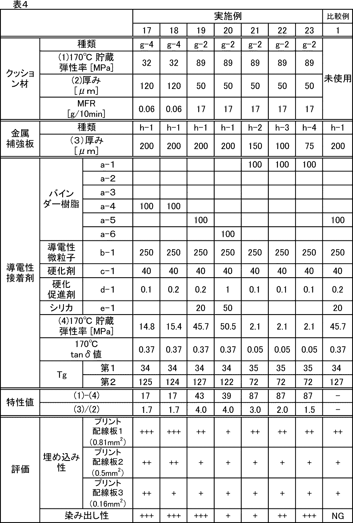
- Examples 2 to 23 The same operation as in Example 1 was performed except that the types and amounts of each component to be blended were as described in Tables 2 to 4, and member sets and printed wiring boards with metal reinforcing plates of Examples 2 to 23 were obtained. rice field.
- Example 1 A member set and a printed wiring board with a metal reinforcing plate were obtained using printed wiring boards 1 to 3 in the same manner as in Example 19, except that no cushion material was used during hot pressing.
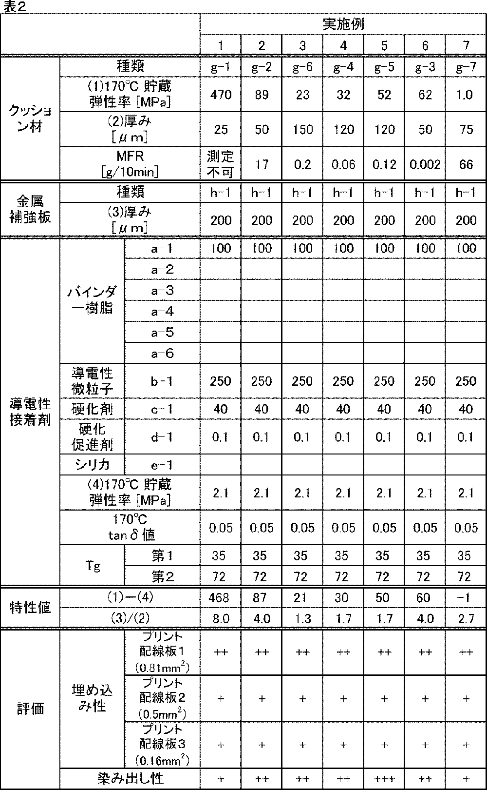
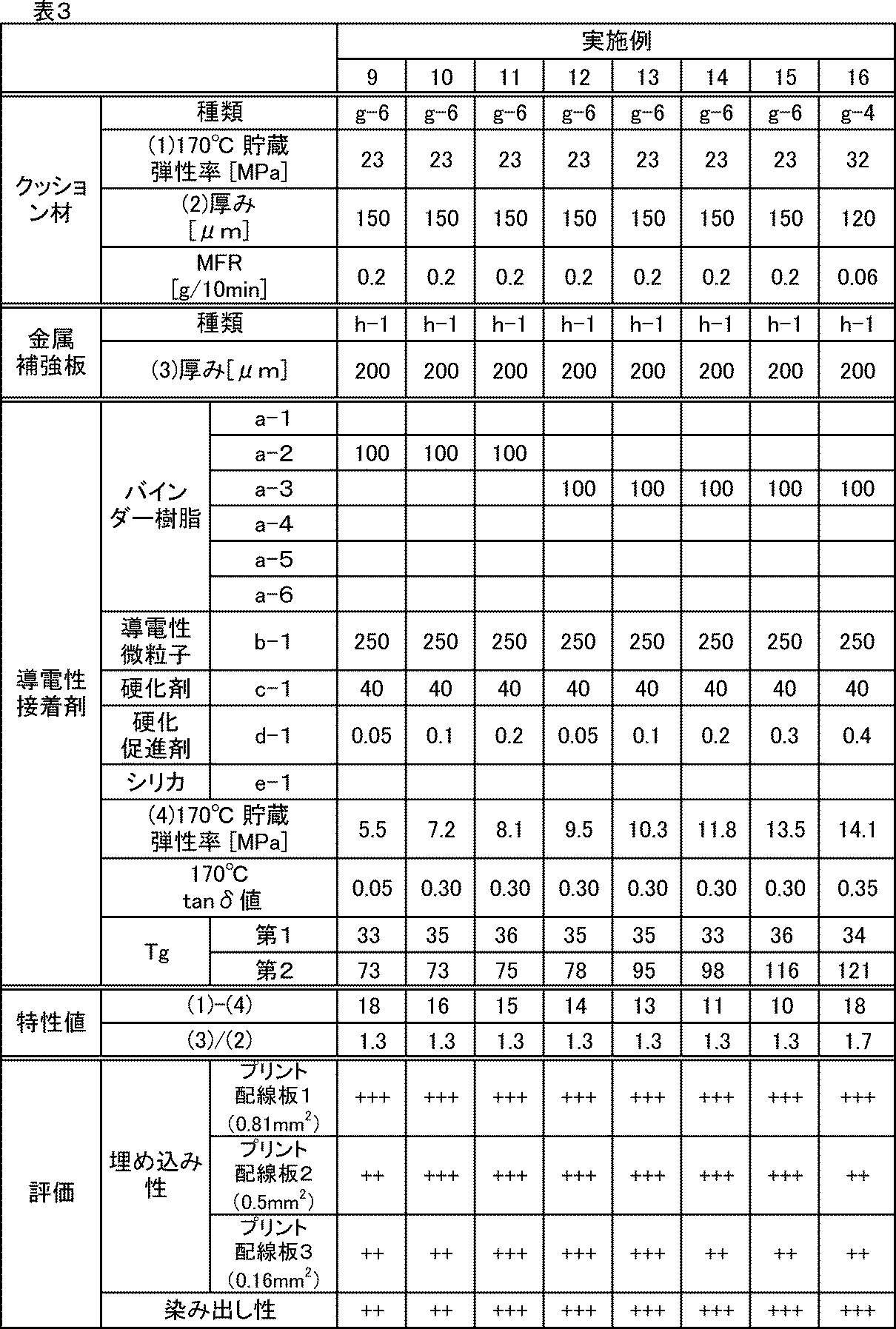
- Tables 2 to 4 show the 170° C. storage elastic modulus (MPa) of the cushion material of each example ⁇ 170° C. storage elastic modulus (MPa) of the conductive adhesive (characteristic values "(1)-(4)” in the table). ), and the value of thickness ( ⁇ m) of metal reinforcing plate/thickness ( ⁇ m) of cushion material (characteristic value “(3)/(2)” in the table).
- the member set is hot-pressed at 150 to 190° C., the ground circuit and the metal reinforcing plate are electrically connected through the opening, and the ground circuit and the metal reinforcing plate are connected by the conductive adhesive.
- the conductive adhesive has a storage modulus of 5.5 MPa or more and 50 MPa or less at 170°C
- the cushion material has a storage modulus of 10 MPa or more and 100 MPa or less at 170°C.
- a method for producing a printed wiring board with a metal reinforcing plate according to any one of 1 to 7. (Appendix 10) In any one of steps [1-1] to [1-3], A laminate obtained by laminating the conductive adhesive, the metal reinforcing plate, and the cushion material in this order is obtained in advance, and the printed wiring board and the conductive adhesive in the laminate face each other.
- Appendix 11 A printed wiring board with a metal reinforcing plate obtained by the manufacturing method according to any one of Appendices 1 to 10. (Appendix 12) 12.
- Appendix 13 13
Landscapes
- Engineering & Computer Science (AREA)
- Microelectronics & Electronic Packaging (AREA)
- Manufacturing & Machinery (AREA)
- Physics & Mathematics (AREA)
- Electromagnetism (AREA)
- Chemical & Material Sciences (AREA)
- Organic Chemistry (AREA)
- Structure Of Printed Boards (AREA)
Abstract
Description
一方、プレス工程のプレス圧によって金属補強板とFPCの間から導電性接着剤の染み出しが生じると、外観不良及び短絡の原因となり、問題となっていた。
本発明の一態様にかかる金属補強板付きプリント配線板の製造方法は、グランド回路を含む回路パターンと、前記回路パターンを絶縁保護し、開口部を有する絶縁保護膜とが形成されたプリント配線板の上方に、熱により軟化するバインダー樹脂および導電性フィラーを含有する導電性接着剤と、金属補強板と、クッション材とがこの順に配置された部材セットを、前記プリント配線板と前記導電性接着剤が対向するように配置する工程[1]、
前記部材セットを熱プレスし、前記絶縁保護膜に設けられた開口部を介して、前記導電性接着剤により前記グランド回路と前記金属補強板とを接着すると共に、前記グランド回路と前記金属補強板とを電気的に接続する工程[2]、ならびに
前記部材セットの前記クッション材を剥離する工程[3]、を備える。
また、本発明の一態様にかかる部材セットは、グランド回路を含む回路パターン、および当該回路パターンを絶縁保護し、前記グランド回路まで貫通する開口部が形成された絶縁保護膜を有するプリント配線板と、前記プリント配線板に熱プレスにより接合された金属補強板とを備える、金属補強板付きプリント配線板の製造に用いる部材セットであって、
熱により軟化するバインダー樹脂および導電性フィラーを含有し、前記熱プレスによって前記開口部に充填されて前記グランド回路と前記金属補強板とを電気的に導通させ、且つ当該金属補強板を前記プリント配線板に接合する導電性接着剤と、前記金属補強板と、前記熱プレス時に軟化して、前記導電性接着剤および前記金属補強板の側面側に流れ込むクッション材と、がこの順で配置される。
図1A~図2Cを用いて金属補強板付きプリント配線板の製造方法について説明する。図2A~図2Cでは、プリント配線板に導電性接着剤を用いて金属補強板を貼り付ける際の製造工程を示している。尚、各々の部材を構成する材料の詳細については後述する。また、本明細書において、「導電性接着剤」は、熱硬化前の導電性接着剤を示し、「導電性接着剤層」は導電性接着剤を熱硬化することで得られた層(つまり、熱硬化後の導電性接着剤)を示すものとし、両者には同一の符号を付す。
まず、図1Aの準備工程[1]に示すように、剥離性フィルム11上に導電性接着剤12が形成された導電性接着シート13と、金属補強板14と、を準備する。そして、図1Bの準備工程[2]に示すように、金属補強板14に導電性接着シート13の導電性接着剤12側を貼り付けて、金属補強板14に導電性接着シート13を仮貼りする。金属補強板14に導電性接着シート13を仮貼りする際の温度(仮貼り温度)は、例えば110℃~150℃、好ましくは130℃とすることができる。仮貼り後、導電性接着剤12は半硬化状態である。
まず、グランド回路を含む回路パターンと、前記回路パターンを絶縁保護し、開口部を有する絶縁保護膜が形成されたプリント配線板を用意する。そして、プリント配線板の絶縁保護膜の上方に、熱により軟化するバインダー樹脂および導電性フィラーを含有する導電性接着剤と、金属補強板と、クッション材とをこの順に有する部材セットを、前記配線板と前記導電性接着剤が対向するように配置する工程である。
工程[2]は、部材セットを熱プレスし、プリント配線板の絶縁保護膜に設けられた開口部を介して、導電性接着剤により前記グランド回路と金属補強板とを接着すると共に、前記グランド回路と金属補強板とを電気的に接続する工程である。
工程[3]は、部材セットのクッション材を剥離する工程である。
熱プレスの後、図2Cに示すように、温度が低下し流動性が消滅したクッション材16を吸引剥離装置又は手作業で剥離する。
これにより、図3に示すように導電性接着剤層12を介して金属補強板14と配線板20のグランド回路25とが電気的に接続された電磁波シールド性を備えた金属補強板付きプリント配線板30を製造することができる。
<部材セット>
本実施の形態にかかる部材セットは、上述した金属補強板付きプリント配線板の製造方法に用いられるものであって、クッション材、金属補強板および導電性接着剤の順に配置される。図4Aに示すように各部材の平面視上のサイズを実質的に同一としてもよい。また、図4Bに示すように、金属補強板および導電性接着剤の平面視上の外縁の外側に、当該金属補強板および導電性接着剤が重畳されていないクッション材の突出領域を有する態様としてもよい。即ち、クッション材の平面視上のサイズを導電性接着剤および金属補強板より大きくし、且つクッション材が金属補強板等より平面視上突出する領域を有する態様としてもよい。かかる構成により、熱プレス時に、導電性接着剤層の側面側への染み出しをより効果的に防止することができる。
また、本発明の部材セットは、染み出し性を防止する観点からは、クッション材の貯蔵弾性率が、170℃において10MPa以上100MPa以下であり、前記導電性接着剤の貯蔵弾性率が、170℃において2MPa以上50MPa以下であり、且つ前記クッション材の貯蔵弾性率が、前記導電性接着剤の貯蔵弾性率よりも高いことが好ましい。
(I)導電性接着剤の170℃における貯蔵弾性率が5.5MPa以上50MPa以下であり、クッション材の170℃における貯蔵弾性率が10MPa以上100MPa以下であって、貯蔵弾性率が導電性接着剤よりもクッション材が高い部材セット。
(II)導電性接着剤の170℃における貯蔵弾性率が2MPa以上50MPa以下であり、クッション材の170℃における貯蔵弾性率が10MPa以上100MPa以下であって、貯蔵弾性率が導電性接着剤よりもクッション材の方が21MPa以上50MPa以内の範囲で高い部材セット。
(III)導電性接着剤の170℃における貯蔵弾性率が2MPa以上50MPa以下であり、クッション材の170℃における貯蔵弾性率が10MPa以上100MPa以下であり、貯蔵弾性率が導電性接着剤よりもクッション材が高く、更に、金属補強板とクッション材の厚みの比率(金属補強板の厚み[μm]/クッション材の厚み[μm])が1.5~2である部材セット。
以下、各層について詳細に説明する。
クッション材は、熱プレス機のプレス圧を均一に金属補強板及び導電性接着剤に伝え、熱プレス時に流動し、導電性接着剤の染み出しを抑制する役割を有する。
金属補強板は、例えば金、銀、銅、鉄およびステンレスの導電性金属が挙げられる。これらの中で補強板としての強度、コストおよび化学的安定性の面でステンレスが好ましい。
本実施の形態にかかる導電性接着剤は、熱により軟化するバインダー樹脂と導電性フィラーとを少なくとも含み、下記の特性を備えることが好ましい。
本実施の形態では、導電性接着剤の170℃における貯蔵弾性率を2MPa以上50MPa以下、好ましくは4MPa以上25MPa以下、更に好ましくは7MPa以上15MPa以下としてもよい。導電性接着剤の170℃における貯蔵弾性率をこの範囲とすることで、熱プレス時(図2Aの工程[1]~図2Cの工程[3]参照)に導電性接着剤12を十分に軟化させることができ、導電性接着剤12の開口部への充填性を向上させることができる。したがって、導電性接着剤12とグランド回路25との間に隙間29b(図5A参照)が形成されることを抑制することができ、金属補強板14とグランド回路25との間の抵抗値が高くなることを抑制することができる。また、導電性接着剤が過剰に軟化することで染み出しが悪化することを抑制することができる(図5B参照)。
本実施の形態では、導電性接着剤の170℃における損失正接(tanδ)は、0.05以上0.4以下が好ましく、0.15以上0.35以下がより好ましく、0.20以上0.3以下がさらに好ましい。導電性接着剤の170℃における損失正接(tanδ)をこの範囲とすることで、導電性接着剤12の開口部への充填性を更に向上させることができる。
また、本実施の形態の導電性接着剤は、粘弾性測定により得られる温度-損失正接(tanδ)曲線におけるピークの温度を用いて求めることができる。本発明の導電接着剤は第1と第2のガラス転移温度を有することが好ましく、低温側のピークを第1のガラス転移温度、高温側のピークを第2のガラス転移温度と定義する。第1のガラス転移温度は10℃以上45℃以下、第2のガラス転移温度は70℃以上140℃以下であることが好ましい。第1のガラス転移温度が25℃以上40℃以下、第2のガラス転移温度が75℃以上110℃以下であることがより好ましい。第1のガラス転移温度が27℃以上36℃以下、第2のガラス転移温度が78℃以上95℃以下であることがさらに好ましい。導電性接着剤のガラス転移温度をこのような範囲とすることで、導電性接着剤の密着性、開口部への充填性を更に向上させることができる。
第2のガラス転移温度を70℃以上140℃以下とするためには、上記と同様の手法により調整することができる。
導電性接着剤の厚さは、15~70μmが好ましく、20~65μmがより好ましい。厚さを15μm以上とすることで小開口ビアへの埋め込み性を向上できる。厚さを70μm以下とすることで染み出し性を抑制できる。導電性接着剤の厚さの測定方法は、接触式の膜厚計、断面観察による計測などで測定することができる。
部材セットを構成する導電性接着剤は、例えば、導電性樹脂組成物を用い、剥離性フィルム上に導電性接着剤を形成した導電性接着シートにより製造することができる。
本実施の形態にかかる導電性接着剤は、熱により軟化するバインダー樹脂、および導電性微粒子を含む導電性樹脂組成物により形成されることが好ましい。
熱硬化性樹脂は、加熱による架橋反応に利用できる官能基を複数有する樹脂である。
官能基は、例えば、水酸基、フェノール性水酸基、カルボキシル基、アミノ基、エポキシ基、オキセタニル基、オキサゾリン基、オキサジン基、アジリジン基、チオール基、イソシアネート基、ブロック化イソシアネート基、シラノール基等が挙げられる。
上記の官能基を有する熱硬化性樹脂は、例えば、アクリル樹脂、マレイン酸樹脂、ポリブタジエン系樹脂、ポリエステル樹脂、縮合型ポリエステル樹脂、付加型ポリエステル樹脂、メラミン樹脂、ポリウレタン樹脂、ポリウレタンウレア樹脂、エポキシ樹脂、オキセタン樹脂、フェノキシ樹脂、ポリイミド樹脂、ポリアミド樹脂、ポリアミドイミド樹脂、フェノール系樹脂、アルキド樹脂、アミノ樹脂、ポリ乳酸樹脂、オキサゾリン樹脂、ベンゾオキサジン樹脂、シリコーン樹脂、フッ素樹脂が挙げられる。これらの中でも、ポリウレタン樹脂、ポリウレタンウレア樹脂、エポキシ樹脂、付加型ポリエステル樹脂、ポリイミド樹脂、ポリアミド樹脂、ポリアミドイミド樹脂が好ましい。
硬化剤は、熱硬化性樹脂の種類に応じて任意に選択できる。硬化剤として、架橋反応により導電性接着剤を形成する際に半硬化状態にするために機能し、導電性接着シート形成の際には完全硬化せず、配線板または金属補強板に熱プレスする際に硬化するような硬化剤も適宜選択できる。硬化剤は、エポキシ系化合物、イソシアネート系硬化剤、アミン系硬化剤、アジリジン系硬化剤、イミダゾール系硬化剤が挙げられる。
本実施の形態では熱可塑性樹脂を併用してもよい。熱可塑性樹脂としては、前記硬化性官能基を有しないポリオレフィン系樹脂、ビニル系樹脂、スチレン・アクリル系樹脂、ジエン系樹脂、テルペン樹脂、石油樹脂、セルロース系樹脂、ポリアミド樹脂、ポリウレタン樹脂、ポリエステル樹脂、ポリカーボネート樹脂、ポリイミド系樹脂、フッ素樹脂などが挙げられる。
ジエン系樹脂は、ブタジエンやイソプレン等の共役ジエン化合物のホモポリマーまたはコポリマーおよびそれらの水素添加物が好ましい。具体的には、例えば、スチレン-ブタジエンゴム、スチレン-イソプレンブロックコポリマー等が挙げられる。テルペン樹脂は、テルペン類からなるポリマーまたはその水素添加物が好ましい。具体的には、例えば、芳香族変性テルペン樹脂、テルペンフェノール樹脂、水添テルペン樹脂が挙げられる。
導電性微粒子は、金、白金、銀、銅およびニッケル等の導電性金属、およびその合金、ならびに導電性ポリマーの微粒子が好ましい。また単一組成の微粒子ではなく金属や樹脂を核体とし、前記核体の表面を被覆する被覆層を核体よりも導電性が高い素材で形成した複合微粒子がコストダウンの観点から好ましい。
核体は、価格が安いニッケル、シリカ、銅およびその合金、ならびに樹脂から適宜選択することが好ましい。
被覆層は、導電性を有する素材であればよく、導電性金属または導電性ポリマーが好ましい。導電性金属は、金、白金、銀、錫、マンガン、およびインジウム等、ならびにその合金が挙げられる。また導電性ポリマーは、ポリアニリン、ポリアセチレン等が挙げられる。これらの中でも導電性の面から銀が好ましい。
導電性微粒子は、単独で用いてもよく、2種類以上を併用してもよい。
剥離性フィルムは、片面あるいは両面に離型処理をしたフィルムであれば制限なく使用することができる。
剥離性フィルムの基材の一例としては、ポリエチレンテレフタレート、ポリエチレンナフタレート、ポリフッ化ビニル、ポリフッ化ビニリデン、硬質ポリ塩化ビニル、ポリ塩化ビニリデン、ナイロン、ポリイミド、ポリスチレン、ポリビニルアルコール、エチレン・ビニルアルコール共重合体、ポリカーボネート、ポリアクリロニトリル、ポリブテン、軟質ポリ塩化ビニル、ポリフッ化ビニリデン、ポリエチレン、ポリプロピレン、ポリウレタン、エチレン酢酸ビニル共重合体、ポリ酢酸ビニル等のプラスチックシート等、グラシン紙、上質紙、クラフト紙、コート紙等の紙類、各種の不織布、合成紙、金属箔や、これらを組み合わせた複合フィルムなどが挙げられる。
プリント配線板は、基材上に、グランド回路を含む回路パターンと前記回路パターンを絶縁保護し、開口部を有する絶縁保護膜を備える。グランド回路を含む回路パターンは銅をエッチングして形成されることが一般的である。絶縁保護膜はポリイミドフィルムと絶縁性接着剤からなるポリイミドカバーレイまたは、レジストフィルム、ソルダーレジストによって形成することが好ましい。グランド回路上の開口部を形成する方法としてドリル加工、エッチング加工、レーザー加工が好ましい。開口部の面積および形状等については後述する。
本実施の形態にかかる金属補強板付きプリント配線板30(図3参照)は、基材21上にグランド回路25を含む回路パターンが配置されており、その上層に絶縁保護する絶縁保護膜(絶縁性フィルム22および絶縁性接着剤23)が形成された配線板20を有する。そして、絶縁保護膜に設けられた開口部27を介して露出しているグランド回路25と、配線板20上に配置され、上述の導電性接着剤を用いて構成された導電性接着剤層12と、導電性接着剤層12上に配置され、導電性接着剤層12を介して配線板20と接着されている金属補強板14と、を備える。本実施の形態にかかる金属補強板付きプリント配線板30は、導電性接着剤層12の一部が開口部27に充填されることで、グランド回路25と金属補強板14とが導電性接着剤層12を介して電気的に接続されている。配線板20には更に信号回路24が設けられていてもよい。
本発明の金属補強板付きプリント配線板の製造方法により、開口部の面積が小さい場合にも、充分に導電性接着剤の充填が可能であり、埋め込み性が良好な金属補強板付きプリント配線板とすることができる。
本実施形態にかかる部材セットは、複数のプリント配線板がアレイ状に形成された大判サイズのマザー基板に対して、一括もしくは分割して金属補強板を接合するために用いてもよい。例えば、m行×n列(m、nはそれぞれ独立に1以上の整数であり、少なくとも一方は2以上である)の区画それぞれにプリント配線板が形成された大判のマザー基板に対し、導電性接着剤および金属板からなる予備積層体を配置し、その上層に大判のクッション材を配置することにより、導電性接着剤/金属板/クッション材からなる部材セットを得、熱プレスにより一括して金属補強板付きプリント配線板を複数有するマザー基板を製造してもよい。また、大判のクッション材に代えて、それぞれのプリント配線板に対応するクッション材を配置したり、複数枚のクッション材を、複数のプリント配線板に亘って配置したりして、同様の工程により一括または/及び分割して金属補強板付きプリント配線板を複数有するマザー基板を製造してもよい。
また、表中の配合量は、重量部であり、溶剤以外は、不揮発分換算値である。尚、表中の空欄は配合していないことを表す。
重量平均分子量(Mw)は、GPC(ゲルパーミエーションクロマトグラフィー)測定で求めたポリスチレン換算の数値である。測定条件は、以下のとおりである。
装置:Shodex GPC System-21(昭和電工製)
カラム:1本のShodex KF-802(昭和電工製)と、1本のShodex KF-803L(昭和電工製)と、1本のShodex KF-805L(昭和電工製)とを直列に連結した連結カラム
溶媒:テトラヒドロフラン
流速:1.0mL/min
温度:40℃
試料濃度:0.2%
試料注入量:100μL
[酸価]
JIS K 0070の電位差滴定法に準拠し、測定した酸価(mgKOH/g)を固形分換算することで求めた。
[ガラス転移温度(Tg)]
熱硬化性樹脂のガラス転移温度の測定は、示差走査熱量計(型番:DSC-1、メトラー・トレド製)を用いて測定した。
[貯蔵弾性率]、[第1、第2のガラス転移温度]および[損失正接tanδ]
動的弾性率測定装置(型番:DVA-200、アイティー計測制御製)を用い、後述の方法により作製した導電性接着シートの剥離性フィルムから剥離した導電性接着剤に対して、変形様式「引張り」、周波数10Hz、昇温速度10℃/分、測定温度範囲-50~300℃の条件下において170℃における貯蔵弾性率E’、損失正接tanδの第1ピーク温度(第1のガラス転移温度)および第2ピーク温度(第2のガラス転移温度)、並びに170℃における損失正接tanδを測定した。クッション材についても同様の方法により求めた。
[メルトフローレート(MFR)]
メルトインデクサ (型式EB01、東洋精機製)を用い、JIS K7210に準拠して各クッション材のMFRを測定した。測定温度は230℃、荷重は10kgとした。尚、異なる材質の層を重ね合わせて形成したクッション材についてはあらかじめ190℃の2本ロールで練り、異なる材質の層の積層状態を混練して均一化した後にMFRを測定した。
実施例および比較例において使用した各部材セットおよび金属補強板付きプリント配線板の作製に用いる導電性樹脂組成物の各材料、クッション材、金属補強板を以下に示す。尚、表1にバインダー樹脂のMw、酸価およびTgを示す。
バインダー樹脂(a-1~6):ポリウレタン系樹脂(トーヨーケム製)

b-1:銀コート銅粒子、D50平均粒子径=12μm、核体:樹枝状(福田金属製)
[硬化剤]
c-1:ビスフェノールA型エポキシ樹脂:エポキシ当量189g/eq(jER1001、三菱ケミカル製)
[硬化促進剤]
d-1:アジリジン化合物(トリメチロールプロパントリス〔β-(N-アジリジニル)プロピオネート〕、日本触媒製)
[その他の成分]
e-1:シリカ(AEROSIL R974、日本アエロジル製)
[溶媒]
f-1:トルエン:イソプロピルアルコール(質量比=2:1)の混合溶媒
[クッション材]
g-1:ポリエチレンテレフタレート(厚み25μm、170℃貯蔵弾性率470MPa、MFR測定不可)
g-2:ポリブチレンテレフタレート(厚み50μm、170℃貯蔵弾性率89MPa、MFR17g/10min)
g-3:ポリメチルペンテン(厚み50μm、170℃貯蔵弾性率62MPa、MFR0.002g/10min)
g-4:ポリメチルペンテン/スチレン-エチレン-ブチレン-スチレンブロックコポリマー/ポリメチルペンテンの3層からなるクッション材(厚み25μm/70μm/25μm、170℃貯蔵弾性率32MPa、MFR0.06g/10min)
g-5:ポリメチルペンテン/スチレン-ブタジエン-スチレンブロックコポリマー/ポリメチルペンテンの3層からなるクッション材(厚み25μm/100μm/25μm、170℃貯蔵弾性率51MPa、MFR0.2g/10min)
g-6:ポリメチルペンテン/エチレン-メタクリル酸グリシジル共重合体/ポリメチルペンテンの3層からなるクッション材(厚み25μm/100μm/25μm、170℃貯蔵弾性率23MPa、MFR0.2g/10min)
g-7:軟質塩化ビニル(厚み75μm、170℃貯蔵弾性率1MPa、MFR66g/10min)
[金属補強板]
h-1:両表面に厚さ2μmのニッケル層を形成した総厚200μmのSUS304
h-2:両表面に厚さ2μmのニッケル層を形成した総厚150μmのSUS304
h-3:両表面に厚さ2μmのニッケル層を形成した総厚100μmのSUS304
h-4:両表面に厚さ2μmのニッケル層を形成した総厚75μmのSUS304
[プリント配線板]
プリント配線板1:プリント配線板1は、厚み75μmのポリイミドフィルムの両面それぞれに厚み32μmの銅箔回路が形成されている。この銅箔回路上には、一辺が0.7mmの正方形であって開口面積が0.49mm2のスルーホール(開口部)を有する厚み37.5μmの接着剤付き絶縁性カバーフィルムが形成されている。また、もう一方の銅箔回路上にはスルーホールを有さない接着剤付きの厚み37.5μmの絶縁性のカバーフィルムが形成されたものである(プリント配線板が反らないように、ポリイミドフィルムに対して銅箔回路およびカバーフィルムを対称に配置した)。
プリント配線板2:一辺が0.4mmの正方形であってスルーホール(開口部)の開口面積が0.16mm2である以外は、プリント配線板1と同様の構成を有するプリント配線板である。
プリント配線板3:一辺が0.2mmの正方形であってスルーホール(開口部)の開口面積を0.04mm2である以外は、プリント配線板1と同様の構成を有するプリント配線板である。
バインダー樹脂(a-1)100重量部、および導電性微粒子(b-1)250重量部を容器に仕込み、不揮発分濃度が40重量%となるように溶媒(f-1)を加えて混合した。次いで、硬化剤(c-1)40重量部、および硬化促進剤(d-1)0.05重量部を加え、攪拌機により10分間攪拌して導電性樹脂組成物を調製した。
次に、上記調製した導電性樹脂組成物を、ドクターブレードを使用して、乾燥後の厚みが60μmになるように剥離性フィルム(基材の材質:発泡ポリエチレンテレフタレート、基材の厚み50μm、離型剤:アルキッド系離型剤)の剥離処理された一方の面上に塗工し、100℃の電気オーブンで2分間乾燥することで導電性接着剤が形成された導電性接着シートを得た。
配合する各成分の種類および配合量を表2~4に記載した通りとした以外は実施例1と同様に操作し、各実施例2~23の部材セット並びに金属補強板付きプリント配線板を得た。
熱プレス時にクッション材を用いなかった以外は、実施例19と同様にして、プリント配線板1~3を用い、部材セットおよび金属補強板付きプリント配線板を得た。
得られた各金属補強板付きプリント配線板について、埋め込み性、および染み出し外観を下記方法に従って評価した。その評価結果を表2~4に示す。
異なる開口面積を有する金属補強板付きプリント配線板1~3について、抵抗値測定器およびBSPプローブ(型番:MCP-TP05P、三菱ケミカルアナリテック製)を用い、金属補強板付きプリント配線板のSUS板と銅箔回路との間の電気抵抗(接続抵抗値)を測定し、この測定値を指標として下記評価基準に従い埋め込み性を評価した。
+++:接続抵抗値が20mΩ/□未満、非常に良好。
++:接続抵抗値が20mΩ/□以上100mΩ/□未満、良好。
+:接続抵抗値が100mΩ/□以上300mΩ/□未満、実用可能。
NG:接続抵抗値が300mΩ/□以上、実用不可能。
金属補強板付きプリント配線板1について、倍率200倍~1000倍の拡大鏡を用いて金属補強板の端部からはみ出した導電性接着剤のフロー量(導電性接着剤層の縁部の最大移動距離、SUS板の端部とはみ出した導電性接着剤層の端部との最大長さ)を測定し、この測定値を指標として下記評価基準に従い外観を評価した。
+++:フロー量が100μm以下、非常に良好。
++:フロー量が100μm超130μm以下、良好。
+:フロー量が130μm超150μm以下、実用可能。
NG:フロー量が150μm超、実用不可能。
(付記1)
グランド回路を含む回路パターンと、前記回路パターンを絶縁保護し、開口部を有する絶縁保護膜とが形成されたプリント配線板の上方に、
熱により軟化するバインダー樹脂および導電性フィラーを含有する導電性接着剤と、厚みが50~500μmの金属補強板と、170℃における貯蔵弾性率が前記導電性接着剤よりも高いクッション材とをこの順で配置された部材セットを、
前記プリント配線板と前記導電性接着剤が対向するように配置する工程[1]、
前記部材セットを150~190℃で熱プレスし、前記開口部を介して前記グランド回路と前記金属補強板とを電気的に接続し、前記導電性接着剤により前記グランド回路と前記金属補強板とを接着すると共に、前記クッション材が、前記導電性接着剤および前記金属補強板の側面側に流れ込み、前記金属補強板よりも外部への前記導電性接着剤の染み出しをせき止める工程[2]、ならびに
前記クッション材を剥離する工程[3]、
を備え、
前記工程[1]において、工程[1-1]~工程[1-3]のいずれかを満たす金属補強板付きプリント配線板の製造方法。
工程[1-1]:前記導電性接着剤の170℃における貯蔵弾性率が5.5MPa以上50MPa以下であり、前記クッション材の170℃における貯蔵弾性率が10MPa以上100MPa以下である。
工程[1-2]:前記導電性接着剤の170℃における貯蔵弾性率が2MPa以上50MPa以下であり、前記クッション材の170℃における貯蔵弾性率が10MPa以上100MPa以下であって、前記170℃における貯蔵弾性率が、前記導電性接着剤よりも前記クッション材の方が21MPa以上50MPa以内の範囲で高い。
工程[1-3]:前記導電性接着剤の170℃における貯蔵弾性率が2MPa以上50MPa以下であり、前記クッション部材の170℃における弾性率が10MPa以上100MPa以下であって、前記金属補強板の厚み[μm]/前記クッション材の厚み[μm]が1.5~2である。
(付記2)
工程[1-1]または工程[1-3]において、前記クッション材と前記導電性接着剤の170℃における貯蔵弾性率差は、10~87MPaである、付記1記載の金属補強板付きプリント配線板の製造方法。
(付記3)
工程[1-1]または工程[1-2]において、前記金属補強板と前記クッション材の厚みの比率(金属補強板の厚み[μm]/クッション材の厚み[μm])が、2以下である、付記1または2記載の金属補強板付きプリント配線板の製造方法。
(付記4)
工程[1-1]~[1-3]いずれか1つの工程において、
170℃における損失正接(tanδ)が0.05以上、0.4以下である、前記導電性接着剤を用いることを特徴とする、
付記1~3いずれかに記載の金属補強板付きプリント配線板の製造方法。
(付記5)
工程[1-1]~[1-3]いずれか1つの工程において、
粘弾性測定により得られる温度-損失正接(tanδ)曲線における、
第1のガラス転移温度が10℃以上45℃以下であり、
第2のガラス転移温度が70℃以上140℃以下である、
前記導電性接着剤を用いることを特徴とする、
付記1~4いずれかに記載の金属補強板付きプリント配線板の製造方法。
(付記6)
工程[1-1]~[1-3]いずれか1つの工程において、
平面視した際に、前記金属補強板および前記導電性接着剤よりも大きい前記クッション材を用いることを特徴とする、
付記1~5いずれかに記載の金属補強板付きプリント配線板の製造方法。
(付記7)
工程[1-1]~[1-3]いずれか1つの工程において、
厚みが15~70μmである前記導電性接着剤を用いることを特徴とする、
付記1~6いずれかに記載の金属補強板付きプリント配線板の製造方法。
(付記8)
工程[1-1]~[1-3]いずれか1つの工程において、
前記プリント配線板上に、前記導電性接着剤を配置し、
前記導電性接着剤上に、前記金属補強板を配置し、
前記金属補強板上に、前記クッション材を配置することを特徴とする、付記1~7いずれかに記載の金属補強板付きプリント配線板の製造方法。
(付記9)
工程[1-1]~[1-3]いずれか1つの工程において、
前記導電性接着剤と、前記金属補強板との予備積層体を予め得ておき、
前記プリント配線板と前記予備積層体中の前記導電性接着剤とが対向し、前記予備積層体中の前記金属補強板と前記クッション材とが対向するように配置することを特徴とする、付記1~7いずれかに記載の金属補強板付きプリント配線板の製造方法。
(付記10)
工程[1-1]~[1-3]いずれか1つの工程において、
前記導電性接着剤と、前記金属補強板と、前記クッション材とをこの順で積層してなる積層体を予め得ておき、前記プリント配線板と前記積層体中の前記導電性接着剤が対向するように配置することを特徴とする、付記1~7いずれかに記載の金属補強板付きプリント配線板の製造方法。
(付記11)
付記1~10いずれかに記載の製造方法により得られる金属補強板付きプリント配線板。
(付記12)
平面視した際の前記開口部の面積が0.16mm2以上、0.81mm2以下である、付記11記載の金属補強板付きプリント配線板。
(付記13)
前記開口部が、前記プリント配線板の外周の一部に形成されている、付記11または12記載の金属補強板付きプリント配線板。
12 導電性接着剤(導電性接着剤層)
13 導電性接着シート
14 金属補強板
15 予備積層体
16 クッション材
17 部材セット
18 切断線
20 配線板
21 基材
22 絶縁性フィルム
23 絶縁性接着剤
24 信号回路
25 グランド回路
27 開口部
29b 隙間
30 金属補強板付きプリント配線板
Claims (11)
- グランド回路を含む回路パターンと、前記回路パターンを絶縁保護し、開口部を有する絶縁保護膜とが形成されたプリント配線板の上方に、
熱により軟化するバインダー樹脂および導電性フィラーを含有する導電性接着剤と、金属補強板と、クッション材とがこの順に配置された部材セットを、
前記プリント配線板と前記導電性接着剤が対向するように配置する工程[1]、
前記部材セットを熱プレスし、前記絶縁保護膜に設けられた開口部を介して、前記導電性接着剤により前記グランド回路と前記金属補強板とを接着すると共に、前記グランド回路と前記金属補強板とを電気的に接続する工程[2]、ならびに
前記部材セットの前記クッション材を剥離する工程[3]、
を備えた金属補強板付きプリント配線板の製造方法。 - グランド回路を含む回路パターン、および当該回路パターンを絶縁保護し、前記グランド回路まで貫通する開口部が形成された絶縁保護膜を有するプリント配線板と、前記プリント配線板に熱プレスにより接合された金属補強板とを備える、金属補強板付きプリント配線板の製造に用いる部材セットであって、
熱により軟化するバインダー樹脂および導電性フィラーを含有し、前記熱プレスによって前記開口部に充填されて前記グランド回路と前記金属補強板とを電気的に導通させ、且つ当該金属補強板を前記プリント配線板に接合する導電性接着剤と、
前記金属補強板と、
前記熱プレス時に軟化して、前記導電性接着剤および前記金属補強板の側面側に流れ込むクッション材と、がこの順で配置された部材セット。 - 前記熱プレス時に、前記導電性接着剤の側面側への染み出しを防止するために、前記金属補強板および前記導電性接着剤の平面視上の外縁の外側に、当該金属補強板および導電性接着剤が重畳されていない前記クッション材の突出領域がある請求項2記載の部材セット。
- 前記クッション材の貯蔵弾性率は、
170℃において10MPa以上100MPa以下であり、
前記導電性接着剤の貯蔵弾性率は、
170℃において2MPa以上50MPa以下であり、
前記クッション材の貯蔵弾性率は、前記導電性接着剤の貯蔵弾性率よりも高いことを特徴とする請求項2または3記載の部材セット。 - 前記クッション材の230℃荷重10kgにおけるメルトフローレート(MFR)は、0.001g/10min以上、17g/10min以下であることを特徴とする請求項2~4のいずれか1項記載の部材セット。
- 前記導電性接着剤の損失正接(tanδ)は、
170℃において0.05以上0.4以下である、
請求項2~5のいずれか1項記載の部材セット。 - 前記導電性接着剤は、
粘弾性測定により得られる温度-損失正接(tanδ)曲線において、
第1のガラス転移温度が10℃以上45℃以下であり、
第2のガラス転移温度が70℃以上140℃以下である、
請求項2~6いずれか1項記載の部材セット。 - 以下の(I)~(III)の条件のいずれかを満たす請求項2~7のいずれか1項記載の部材セット。
(I)前記導電性接着剤の170℃における貯蔵弾性率が5.5MPa以上50MPa以下であり、前記クッション材の170℃における貯蔵弾性率が10MPa以上100MPa以下であって、前記貯蔵弾性率が前記導電性接着剤よりも前記クッション材が高い。
(II)前記導電性接着剤の170℃における貯蔵弾性率が2MPa以上50MPa以下であり、前記クッション材の170℃における貯蔵弾性率が10MPa以上100MPa以下であって、前記貯蔵弾性率が前記導電性接着剤よりも前記クッション材の方が21MPa以上50MPa以内の範囲で高い。
(III)前記導電性接着剤の170℃における貯蔵弾性率が2MPa以上50MPa以下であり、前記クッション材の170℃における貯蔵弾性率が10MPa以上100MPa以下であり、前記貯蔵弾性率が前記導電性接着剤よりも前記クッション材が高く、更に、前記金属補強板と前記クッション材の厚みの比率(金属補強板の厚み[μm]/クッション材の厚み[μm])が1.5~2である。 - 前記金属補強板の厚みが50~500μmである請求項2~8のいずれか1項記載の部材セット。
- 請求項1記載の製造方法により得られ、
平面視した際の前記開口部の面積が0.16mm2以上0.81mm2以下である金属補強板付きプリント配線板。 - 前記開口部の少なくとも一部が、前記プリント配線板の前記絶縁保護膜の外周の側壁により形成されている、請求項10記載の金属補強板付きプリント配線板。
Priority Applications (3)
| Application Number | Priority Date | Filing Date | Title |
|---|---|---|---|
| KR1020237037117A KR102929822B1 (ko) | 2021-05-12 | 2021-05-12 | 금속 보강판 부착 프린트 배선판의 제조 방법, 부재 세트, 및 금속 보강판 부착 프린트 배선판 |
| PCT/JP2021/018129 WO2022239167A1 (ja) | 2021-05-12 | 2021-05-12 | 金属補強板付きプリント配線板の製造方法、部材セット、及び金属補強板付きプリント配線板 |
| CN202180097940.5A CN117280876A (zh) | 2021-05-12 | 2021-05-12 | 带金属增强板的印刷布线板的制造方法、构件组及带金属增强板的印刷布线板 |
Applications Claiming Priority (1)
| Application Number | Priority Date | Filing Date | Title |
|---|---|---|---|
| PCT/JP2021/018129 WO2022239167A1 (ja) | 2021-05-12 | 2021-05-12 | 金属補強板付きプリント配線板の製造方法、部材セット、及び金属補強板付きプリント配線板 |
Publications (1)
| Publication Number | Publication Date |
|---|---|
| WO2022239167A1 true WO2022239167A1 (ja) | 2022-11-17 |
Family
ID=84028063
Family Applications (1)
| Application Number | Title | Priority Date | Filing Date |
|---|---|---|---|
| PCT/JP2021/018129 Ceased WO2022239167A1 (ja) | 2021-05-12 | 2021-05-12 | 金属補強板付きプリント配線板の製造方法、部材セット、及び金属補強板付きプリント配線板 |
Country Status (3)
| Country | Link |
|---|---|
| KR (1) | KR102929822B1 (ja) |
| CN (1) | CN117280876A (ja) |
| WO (1) | WO2022239167A1 (ja) |
Citations (5)
| Publication number | Priority date | Publication date | Assignee | Title |
|---|---|---|---|---|
| JP2000013031A (ja) * | 1998-06-19 | 2000-01-14 | Hitachi Chem Co Ltd | 多層プリント配線板の製造方法 |
| JP2005154977A (ja) * | 2003-11-28 | 2005-06-16 | Daio Paper Corp | クッション紙 |
| WO2016032006A1 (ja) * | 2014-08-29 | 2016-03-03 | タツタ電線株式会社 | フレキシブルプリント配線板用補強部材、及びそれを備えたフレキシブルプリント配線板 |
| JP2018168323A (ja) * | 2017-03-30 | 2018-11-01 | 信越ポリマー株式会社 | 熱硬化性組成物、硬化物、電磁波シールドフィルム及びその製造方法、並びに電磁波シールドフィルム付きプリント配線板及びその製造方法 |
| JP2021097152A (ja) * | 2019-12-18 | 2021-06-24 | 東洋インキScホールディングス株式会社 | 金属補強板付きプリント配線板の製造方法、積層体、及び金属補強板付きプリント配線板 |
Family Cites Families (4)
| Publication number | Priority date | Publication date | Assignee | Title |
|---|---|---|---|---|
| TWI476103B (zh) * | 2003-07-01 | 2015-03-11 | Sumitomo Bakelite Co | A release film and a method of manufacturing a flexible printed wiring board using the release film |
| CN104487534B (zh) | 2012-07-11 | 2016-11-09 | 大自达电线股份有限公司 | 硬化导电胶组成物、电磁波屏蔽膜、导电胶膜、黏合方法及线路基板 |
| TWI727167B (zh) | 2017-08-07 | 2021-05-11 | 日商拓自達電線股份有限公司 | 導電性接著劑 |
| JP6904464B2 (ja) * | 2019-06-12 | 2021-07-14 | 東洋インキScホールディングス株式会社 | プリント配線板 |
-
2021
- 2021-05-12 KR KR1020237037117A patent/KR102929822B1/ko active Active
- 2021-05-12 WO PCT/JP2021/018129 patent/WO2022239167A1/ja not_active Ceased
- 2021-05-12 CN CN202180097940.5A patent/CN117280876A/zh active Pending
Patent Citations (5)
| Publication number | Priority date | Publication date | Assignee | Title |
|---|---|---|---|---|
| JP2000013031A (ja) * | 1998-06-19 | 2000-01-14 | Hitachi Chem Co Ltd | 多層プリント配線板の製造方法 |
| JP2005154977A (ja) * | 2003-11-28 | 2005-06-16 | Daio Paper Corp | クッション紙 |
| WO2016032006A1 (ja) * | 2014-08-29 | 2016-03-03 | タツタ電線株式会社 | フレキシブルプリント配線板用補強部材、及びそれを備えたフレキシブルプリント配線板 |
| JP2018168323A (ja) * | 2017-03-30 | 2018-11-01 | 信越ポリマー株式会社 | 熱硬化性組成物、硬化物、電磁波シールドフィルム及びその製造方法、並びに電磁波シールドフィルム付きプリント配線板及びその製造方法 |
| JP2021097152A (ja) * | 2019-12-18 | 2021-06-24 | 東洋インキScホールディングス株式会社 | 金属補強板付きプリント配線板の製造方法、積層体、及び金属補強板付きプリント配線板 |
Also Published As
| Publication number | Publication date |
|---|---|
| KR20230163499A (ko) | 2023-11-30 |
| KR102929822B1 (ko) | 2026-02-24 |
| CN117280876A (zh) | 2023-12-22 |
Similar Documents
| Publication | Publication Date | Title |
|---|---|---|
| KR101794147B1 (ko) | 도전성 접착제 층, 도전성 접착 시트, 프린트 배선판 및 전자 기기 | |
| TWI745273B (zh) | 附有接著劑層之積層體、以及使用其之可撓性覆銅積層板及可撓性扁平電纜 | |
| JP5854248B1 (ja) | 導電性接着剤、ならびにそれを用いた導電性接着シートおよび電磁波シールドシート | |
| JP6904464B2 (ja) | プリント配線板 | |
| JP6578142B2 (ja) | 接着剤組成物、プリント配線板用カバーレイ、プリント配線板用ボンディングフィルム及びプリント配線板 | |
| WO2019239710A1 (ja) | 電磁波シールドシート | |
| TWI784366B (zh) | 黏接劑組成物 | |
| TW201736457A (zh) | 預浸材 | |
| TW202214808A (zh) | 黏接劑組成物 | |
| JP5771988B2 (ja) | 熱硬化性樹脂組成物 | |
| KR102611197B1 (ko) | 도전성 조성물, 도전성 시트, 금속 보강판, 금속 보강판을 포함하는 배선판, 및 전자기기 | |
| TWI754611B (zh) | Fpc用導電性黏著片材及使用此片材之fpc | |
| JP7056723B2 (ja) | 部材セット | |
| JP2018129493A (ja) | 部品搭載基板の製造方法 | |
| JP2004256678A (ja) | 樹脂組成物、カバーレイ及びそれを用いたフレキシブルプリント配線板用銅張積層板 | |
| WO2022239167A1 (ja) | 金属補強板付きプリント配線板の製造方法、部材セット、及び金属補強板付きプリント配線板 | |
| JP2010018676A (ja) | 難燃性接着剤組成物、ならびにそれを用いた接着シート、カバーレイフィルムおよびフレキシブル銅張積層板 | |
| JP4433693B2 (ja) | 樹脂組成物、カバーレイ、フレキシブルプリント配線板用金属張積層板およびフレキシブルプリント配線板 | |
| JP2017183376A (ja) | フレキシブル基板、フレキシブル回路基板および支持体レスフレキシブル回路基板の製造方法 | |
| KR20160108968A (ko) | 커버레이 필름 제조방법 및 연성인쇄회로기판의 제조 방법 | |
| KR102516292B1 (ko) | 전자장치 제조용 절연필름 | |
| KR102560185B1 (ko) | 밀봉용 수지 조성물층, 지지체 부착 수지 시트, 밀봉용 수지 경화층, 반도체 패키지 및 반도체 장치 | |
| JP2019169484A (ja) | 電磁波シールド材 | |
| JP2008063361A (ja) | エポキシ系接着剤、カバーレイ、プリプレグ、金属張積層板、プリント配線基板 | |
| JP2006160994A (ja) | 接着剤組成物、金属張積層板およびフレキシブルプリント配線基板 |
Legal Events
| Date | Code | Title | Description |
|---|---|---|---|
| 121 | Ep: the epo has been informed by wipo that ep was designated in this application |
Ref document number: 21941901 Country of ref document: EP Kind code of ref document: A1 |
|
| ENP | Entry into the national phase |
Ref document number: 20237037117 Country of ref document: KR Kind code of ref document: A |
|
| WWE | Wipo information: entry into national phase |
Ref document number: 202180097940.5 Country of ref document: CN |
|
| NENP | Non-entry into the national phase |
Ref country code: DE |
|
| 122 | Ep: pct application non-entry in european phase |
Ref document number: 21941901 Country of ref document: EP Kind code of ref document: A1 |
|
| NENP | Non-entry into the national phase |
Ref country code: JP |