WO2022230900A1 - 固体電池パッケージ - Google Patents
固体電池パッケージ Download PDFInfo
- Publication number
- WO2022230900A1 WO2022230900A1 PCT/JP2022/018942 JP2022018942W WO2022230900A1 WO 2022230900 A1 WO2022230900 A1 WO 2022230900A1 JP 2022018942 W JP2022018942 W JP 2022018942W WO 2022230900 A1 WO2022230900 A1 WO 2022230900A1
- Authority
- WO
- WIPO (PCT)
- Prior art keywords
- layer
- substrate
- solid
- water vapor
- state battery
- Prior art date
- Legal status (The legal status is an assumption and is not a legal conclusion. Google has not performed a legal analysis and makes no representation as to the accuracy of the status listed.)
- Ceased
Links
Images


Classifications
-
- H—ELECTRICITY
- H01—ELECTRIC ELEMENTS
- H01M—PROCESSES OR MEANS, e.g. BATTERIES, FOR THE DIRECT CONVERSION OF CHEMICAL ENERGY INTO ELECTRICAL ENERGY
- H01M50/00—Constructional details or processes of manufacture of the non-active parts of electrochemical cells other than fuel cells, e.g. hybrid cells
- H01M50/10—Primary casings; Jackets or wrappings
- H01M50/116—Primary casings; Jackets or wrappings characterised by the material
- H01M50/124—Primary casings; Jackets or wrappings characterised by the material having a layered structure
- H01M50/126—Primary casings; Jackets or wrappings characterised by the material having a layered structure comprising three or more layers
-
- H—ELECTRICITY
- H01—ELECTRIC ELEMENTS
- H01M—PROCESSES OR MEANS, e.g. BATTERIES, FOR THE DIRECT CONVERSION OF CHEMICAL ENERGY INTO ELECTRICAL ENERGY
- H01M10/00—Secondary cells; Manufacture thereof
- H01M10/05—Accumulators with non-aqueous electrolyte
- H01M10/056—Accumulators with non-aqueous electrolyte characterised by the materials used as electrolytes, e.g. mixed inorganic/organic electrolytes
- H01M10/0561—Accumulators with non-aqueous electrolyte characterised by the materials used as electrolytes, e.g. mixed inorganic/organic electrolytes the electrolyte being constituted of inorganic materials only
- H01M10/0562—Solid materials
-
- H—ELECTRICITY
- H01—ELECTRIC ELEMENTS
- H01M—PROCESSES OR MEANS, e.g. BATTERIES, FOR THE DIRECT CONVERSION OF CHEMICAL ENERGY INTO ELECTRICAL ENERGY
- H01M10/00—Secondary cells; Manufacture thereof
- H01M10/05—Accumulators with non-aqueous electrolyte
- H01M10/058—Construction or manufacture
- H01M10/0585—Construction or manufacture of accumulators having only flat construction elements, i.e. flat positive electrodes, flat negative electrodes and flat separators
-
- H—ELECTRICITY
- H01—ELECTRIC ELEMENTS
- H01M—PROCESSES OR MEANS, e.g. BATTERIES, FOR THE DIRECT CONVERSION OF CHEMICAL ENERGY INTO ELECTRICAL ENERGY
- H01M50/00—Constructional details or processes of manufacture of the non-active parts of electrochemical cells other than fuel cells, e.g. hybrid cells
- H01M50/10—Primary casings; Jackets or wrappings
- H01M50/102—Primary casings; Jackets or wrappings characterised by their shape or physical structure
- H01M50/11—Primary casings; Jackets or wrappings characterised by their shape or physical structure having a chip structure, e.g. micro-sized batteries integrated on chips
-
- H—ELECTRICITY
- H01—ELECTRIC ELEMENTS
- H01M—PROCESSES OR MEANS, e.g. BATTERIES, FOR THE DIRECT CONVERSION OF CHEMICAL ENERGY INTO ELECTRICAL ENERGY
- H01M50/00—Constructional details or processes of manufacture of the non-active parts of electrochemical cells other than fuel cells, e.g. hybrid cells
- H01M50/10—Primary casings; Jackets or wrappings
- H01M50/116—Primary casings; Jackets or wrappings characterised by the material
- H01M50/117—Inorganic material
- H01M50/119—Metals
-
- H—ELECTRICITY
- H01—ELECTRIC ELEMENTS
- H01M—PROCESSES OR MEANS, e.g. BATTERIES, FOR THE DIRECT CONVERSION OF CHEMICAL ENERGY INTO ELECTRICAL ENERGY
- H01M50/00—Constructional details or processes of manufacture of the non-active parts of electrochemical cells other than fuel cells, e.g. hybrid cells
- H01M50/10—Primary casings; Jackets or wrappings
- H01M50/116—Primary casings; Jackets or wrappings characterised by the material
- H01M50/121—Organic material
-
- H—ELECTRICITY
- H01—ELECTRIC ELEMENTS
- H01M—PROCESSES OR MEANS, e.g. BATTERIES, FOR THE DIRECT CONVERSION OF CHEMICAL ENERGY INTO ELECTRICAL ENERGY
- H01M50/00—Constructional details or processes of manufacture of the non-active parts of electrochemical cells other than fuel cells, e.g. hybrid cells
- H01M50/10—Primary casings; Jackets or wrappings
- H01M50/131—Primary casings; Jackets or wrappings characterised by physical properties, e.g. gas permeability, size or heat resistance
-
- H—ELECTRICITY
- H01—ELECTRIC ELEMENTS
- H01M—PROCESSES OR MEANS, e.g. BATTERIES, FOR THE DIRECT CONVERSION OF CHEMICAL ENERGY INTO ELECTRICAL ENERGY
- H01M50/00—Constructional details or processes of manufacture of the non-active parts of electrochemical cells other than fuel cells, e.g. hybrid cells
- H01M50/50—Current conducting connections for cells or batteries
- H01M50/543—Terminals
- H01M50/547—Terminals characterised by the disposition of the terminals on the cells
-
- Y—GENERAL TAGGING OF NEW TECHNOLOGICAL DEVELOPMENTS; GENERAL TAGGING OF CROSS-SECTIONAL TECHNOLOGIES SPANNING OVER SEVERAL SECTIONS OF THE IPC; TECHNICAL SUBJECTS COVERED BY FORMER USPC CROSS-REFERENCE ART COLLECTIONS [XRACs] AND DIGESTS
- Y02—TECHNOLOGIES OR APPLICATIONS FOR MITIGATION OR ADAPTATION AGAINST CLIMATE CHANGE
- Y02E—REDUCTION OF GREENHOUSE GAS [GHG] EMISSIONS, RELATED TO ENERGY GENERATION, TRANSMISSION OR DISTRIBUTION
- Y02E60/00—Enabling technologies; Technologies with a potential or indirect contribution to GHG emissions mitigation
- Y02E60/10—Energy storage using batteries
Definitions
- the present invention relates to solid-state battery packages. More specifically, the present invention relates to solid state batteries that are packaged to facilitate packaging.
- Secondary batteries that can be repeatedly charged and discharged have been used for various purposes.
- secondary batteries are used as power sources for electronic devices such as smartphones and notebook computers.
- liquid electrolytes are generally used as a medium for ion transfer that contributes to charging and discharging. That is, a so-called electrolytic solution is used in the secondary battery.
- electrolytic solution is used in the secondary battery.
- safety is generally required in terms of preventing electrolyte leakage.
- organic solvent and the like used in the electrolytic solution are combustible substances, safety is required in this respect as well.
- solid-state batteries will be used together with other electronic components mounted on printed wiring boards, etc.
- a structure suitable for mounting is required.
- a package in which a solid-state battery is arranged on a substrate contributes to mounting by making the substrate responsible for electrical connection with the outside.
- a package in which a solid-state battery is arranged on a substrate cannot necessarily be said to be able to sufficiently prevent the infiltration of water vapor from the substrate side.
- the substrate itself is thick enough to block water vapor penetration to some extent, it may not be sufficient for solid-state batteries, and there remains concern that solid-state battery characteristics may deteriorate over the long term.
- the inventors of the present application have found that.
- the present invention has been made in view of such problems. That is, it is a primary object of the present invention to provide a technology for a solid-state battery that has a substrate that contributes to mounting and that can more effectively prevent water vapor permeation associated with the substrate.
- the inventors of the present application have attempted to solve the above problems by dealing with them in a new direction, rather than dealing with them on the extension of the conventional technology. As a result, the inventors have invented a solid-state battery that achieves the above-described main object.
- the present invention provides a solid battery package comprising a substrate and a solid battery provided on the substrate, and having a water vapor barrier layer between the substrate and the solid battery.
- the solid-state battery package according to the present invention has a substrate that contributes to mounting, and is more excellent in preventing water vapor permeation.
- the present invention is a solid-state battery package in which prevention of water vapor permeation through a substrate that contributes to mounting is more appropriately considered.
- a water vapor barrier layer is provided between the substrate and the solid state battery to reduce undesirable permeation of water vapor from the external environment through the substrate and into the solid state battery. Therefore, the solid-state battery package of the present invention is less likely to cause deterioration of solid-state battery characteristics over a long period of time, and has high reliability.
- FIG. 1 is a cross-sectional view schematically showing a solid battery package.
- FIG. 2 is a cross-sectional view schematically showing a solid battery package.
- FIG. 3 is a cross-sectional view schematically showing a solid-state battery package, and is a diagram particularly for explaining "layers constituting a substrate" and "layers constituting a solid-state battery”.
- FIG. 4 is a cross-sectional view schematically showing the solid battery package and a partially enlarged view thereof, and is a view for explaining, in particular, the wide extension form of the water vapor barrier layer.
- FIG. 5 is a cross-sectional view schematically showing the solid battery package and a partially enlarged view thereof, and is a diagram for explanation particularly related to the resist layer.
- FIG. 1 is a cross-sectional view schematically showing a solid battery package.
- FIG. 2 is a cross-sectional view schematically showing a solid battery package.
- FIG. 3 is a cross-sectional view schematically showing a solid
- FIG. 6 is a cross-sectional view schematically showing a solid battery package and a schematic diagram showing a substrate configuration.
- FIG. 7 is a schematic diagram showing each layer constituting the substrate.
- FIG. 8 is a cross-sectional view schematically showing a solid battery package and a plan view showing a metal layer included in a substrate.
- 9A to 9E are process cross-sectional views schematically showing the process of obtaining a solid battery package.
- FIG. 10 is a cross-sectional view schematically showing the solid state battery package, and is a view for explaining a mode particularly related to non-arrangement of the resist.
- FIG. 11 is a cross-sectional view schematically showing the solid battery package, and is a view particularly for explaining the aspect of the covering inorganic layer.
- FIG. 12 is a cross-sectional view schematically showing a solid-state battery package, and is a schematic diagram particularly showing a certain substrate configuration example.
- FIG. 13 is a cross-sectional view schematically showing the solid battery package and a partially enlarged view thereof, and is a diagram for explanation particularly related to the conductive paste.
- solid battery package broadly refers to a solid battery device (or solid battery product) configured to protect the solid battery from the external environment. It refers to a solid-state battery product that is provided with a substrate that contributes to mounting and that protects the solid-state battery from the external environment.
- cross-sectional view refers to a form captured from a direction substantially perpendicular to the stacking direction in the stacking structure of a solid-state battery (straightforwardly, when cut in a plane parallel to the thickness direction of the layer) morphology).
- planar view or “planar view shape” used herein refers to a sketch of the object when viewed from above or below along the thickness direction of the layer (that is, the lamination direction described above). ing. To put it simply, the shape obtained by capturing the target surface from its normal direction can be said to be the “plane view shape”.
- Up-down direction and “left-right direction” used directly or indirectly in this specification correspond to the up-down direction and left-right direction in the drawing, respectively. Unless otherwise specified, the same symbols or symbols shall indicate the same parts and/or parts or the same meaning.
- the downward vertical direction that is, the direction in which gravity acts
- the opposite direction corresponds to the “upward direction”/“top side”.
- solid battery as used in the present invention broadly refers to a battery whose components are solid, and narrowly refers to an all-solid-state battery whose components (particularly preferably all components) are solid.
- the solid-state battery in the present invention is a stacked-type solid-state battery in which layers constituting battery structural units are stacked with each other, and preferably each such layer is made of a sintered body.
- Solid battery includes not only a so-called “secondary battery” that can be repeatedly charged and discharged, but also a "primary battery” that can only be discharged.
- the "solid battery” is a secondary battery.
- Secondary battery is not limited to its name, and can include, for example, power storage devices.
- the solid-state battery contained in the package can also be referred to as a "solid-state battery element.”
- a solid battery comprises at least positive and negative electrode layers and a solid electrolyte.
- the solid battery 100 has a solid battery stack including a battery structural unit consisting of a positive electrode layer 110, a negative electrode layer 120, and at least a solid electrolyte 130 interposed therebetween. It consists
- each layer constituting the battery may be formed by firing, and the positive electrode layer, the negative electrode layer, the solid electrolyte, and the like may form a fired layer.
- the positive electrode layer, the negative electrode layer, and the solid electrolyte are each co-fired with each other, and therefore the solid battery laminate preferably constitutes an co-fired body.
- the positive electrode layer 110 is an electrode layer containing at least a positive electrode active material.
- the positive electrode layer may further comprise a solid electrolyte.
- the positive electrode layer is composed of a sintered body containing at least positive electrode active material particles and solid electrolyte particles.
- the negative electrode layer is an electrode layer containing at least a negative electrode active material.
- the negative electrode layer may further comprise a solid electrolyte.
- the negative electrode layer is composed of a sintered body containing at least negative electrode active material particles and solid electrolyte particles.
- the positive electrode active material and negative electrode active material are substances involved in the transfer of electrons in solid-state batteries. Ions are transferred (or conducted) between the positive electrode layer and the negative electrode layer via the solid electrolyte, and electrons are transferred, whereby charging and discharging are performed.
- Each of the positive electrode layer and the negative electrode layer is preferably a layer capable of intercalating and deintercalating lithium ions or sodium ions. That is, the solid-state battery is preferably an all-solid-state secondary battery in which charge and discharge are performed by moving lithium ions or sodium ions between the positive electrode layer and the negative electrode layer via a solid electrolyte.
- Examples of the positive electrode active material contained in the positive electrode layer 110 include a lithium-containing phosphate compound having a Nasicon type structure, a lithium-containing phosphate compound having an olivine type structure, a lithium-containing layered oxide, and lithium having a spinel type structure. At least one selected from the group consisting of contained oxides and the like can be mentioned.
- Li3V2 ( PO4) 3 etc. are mentioned as an example of the lithium containing phosphate compound which has a Nasicon type structure.
- Examples of lithium-containing phosphate compounds having an olivine structure include Li3Fe2 ( PO4) 3 , LiFePO4 , and/or LiMnPO4 .
- lithium - containing layered oxides examples include LiCoO2 and/or LiCo1 / 3Ni1 / 3Mn1 / 3O2 .
- lithium-containing oxides having a spinel structure examples include LiMn 2 O 4 and/or LiNi 0.5 Mn 1.5 O 4 .
- the type of lithium compound is not particularly limited, for example, a lithium transition metal composite oxide and a lithium transition metal phosphate compound may be used.
- Lithium transition metal composite oxide is a general term for oxides containing lithium and one or more transition metal elements as constituent elements
- lithium transition metal phosphate compounds are lithium and one or more transition metal elements.
- the types of transition metal elements are not particularly limited, but examples include cobalt (Co), nickel (Ni), manganese (Mn) and iron (Fe).
- the positive electrode active material capable of occluding and releasing sodium ions includes a sodium-containing phosphate compound having a Nasicon-type structure, a sodium-containing phosphate compound having an olivine-type structure, a sodium-containing layered oxide, and a spinel-type structure. At least one selected from the group consisting of sodium-containing oxides and the like can be mentioned.
- Na3V2 (PO4) 3 NaCoFe2 (PO4) 3 , Na2Ni2Fe ( PO4) 3 , Na3Fe2 ( PO4 ) 3 , Na 2 FeP 2 O 7 , Na 4 Fe 3 (PO 4 ) 2 (P 2 O 7 ), and at least one selected from the group consisting of NaFeO 2 as the sodium-containing layered oxide.
- the positive electrode active material may be, for example, an oxide, a disulfide, a chalcogenide, or a conductive polymer.
- the oxide may be, for example, titanium oxide, vanadium oxide, manganese dioxide, or the like.
- Disulfides are, for example, titanium disulfide or molybdenum sulfide.
- the chalcogenide may be, for example, niobium selenide.
- the conductive polymer may be, for example, disulfide, polypyrrole, polyaniline, polythiophene, polyparastyrene, polyacetylene, polyacene, or the like.
- the negative electrode active material contained in the negative electrode layer 120 includes, for example, titanium (Ti), silicon (Si), tin (Sn), chromium (Cr), iron (Fe), niobium (Nb), and molybdenum (Mo).
- Examples of lithium alloys include Li—Al and the like.
- Li3V2 ( PO4) 3 and/or LiTi2 ( PO4) 3 etc. are mentioned as an example of the lithium containing phosphate compound which has a Nasicon type structure.
- Examples of lithium - containing phosphate compounds having an olivine structure include Li3Fe2 (PO4)3 and /or LiCuPO4 .
- Li4Ti5O12 etc. are mentioned as an example of the lithium containing oxide which has a spinel type structure.
- a sodium-containing phosphate compound having a Nasicon-type structure a sodium-containing phosphate compound having an olivine-type structure, a sodium-containing oxide having a spinel-type structure, and the like. At least one selected from the group consisting of
- the positive electrode layer and the negative electrode layer may be made of the same material.
- the positive electrode layer and/or the negative electrode layer may contain a conductive material. At least one of metal materials such as silver, palladium, gold, platinum, aluminum, copper and nickel, and carbon can be used as the conductive material contained in the positive electrode layer and the negative electrode layer.
- the positive electrode layer and/or the negative electrode layer may contain a sintering aid.
- Sintering aids include at least one selected from the group consisting of lithium oxide, sodium oxide, potassium oxide, boron oxide, silicon oxide, bismuth oxide and phosphorus oxide.
- the thicknesses of the positive electrode layer and the negative electrode layer are not particularly limited, for example, they may be independently 2 ⁇ m or more and 50 ⁇ m or less, particularly 5 ⁇ m or more and 30 ⁇ m or less.
- the positive electrode layer 110 and the negative electrode layer 120 may each include a positive current collecting layer and a negative current collecting layer.
- the positive current collecting layer and the negative current collecting layer may each have the form of a foil.
- the positive electrode current collecting layer and the negative electrode current collecting layer are in the form of fired bodies, respectively.
- the positive electrode current collector that constitutes the positive electrode current collecting layer and the negative electrode current collector that constitutes the negative electrode current collecting layer it is preferable to use materials having high electrical conductivity, such as silver, palladium, gold, platinum, aluminum, and copper. , and/or nickel, etc. may be used.
- Each of the positive electrode current collector and the negative electrode current collector may have an electrical connection portion for electrical connection with the outside, and may be configured to be electrically connectable to the end face electrode.
- the positive electrode current collecting layer and the negative electrode current collecting layer may be composed of a fired body containing a conductive material and a sintering aid.
- the conductive material contained in the positive electrode current collecting layer and the negative electrode current collecting layer may be selected from, for example, the same conductive materials that can be contained in the positive electrode layer and the negative electrode layer.
- the sintering aid contained in the positive electrode current collecting layer and the negative electrode current collecting layer may be selected, for example, from materials similar to those of the sintering aid that can be contained in the positive electrode layer and the negative electrode layer.
- a positive electrode current collecting layer and a negative electrode current collecting layer are not essential in a solid battery, and a solid battery without such a positive electrode current collecting layer and a negative electrode current collecting layer is also conceivable. That is, the solid-state battery included in the package of the present invention may be a solid-state battery without a current collecting layer.
- a solid electrolyte is a material that can conduct lithium ions or sodium ions.
- the solid electrolyte 130 forming a battery structural unit in a solid battery may form a layer capable of conducting lithium ions between the positive electrode layer 110 and the negative electrode layer 120 .
- the solid electrolyte may be provided at least between the positive electrode layer and the negative electrode layer. That is, the solid electrolyte may exist around the positive electrode layer and/or the negative electrode layer so as to protrude from between the positive electrode layer and the negative electrode layer.
- Specific solid electrolytes include, for example, one or more of crystalline solid electrolytes, glass-based solid electrolytes, glass-ceramics-based solid electrolytes, and the like.
- Crystalline solid electrolytes include, for example, oxide-based crystal materials and sulfide-based crystal materials.
- oxide-based crystal materials include lithium-containing phosphate compounds having a Nasicon structure, oxides having a perovskite structure, oxides having a garnet-type or garnet-like structure, oxide glass-ceramics-based lithium ion conductors, and the like. be done.
- lithium-containing phosphate compounds having a Nasicon structure include LixMy (PO4) 3 ( 1 ⁇ x ⁇ 2 , 1 ⁇ y ⁇ 2 , M is titanium (Ti), germanium (Ge), aluminum (Al ), at least one selected from the group consisting of gallium (Ga) and zirconium (Zr)).
- An example of the lithium-containing phosphate compound having a Nasicon structure includes Li 1.2 Al 0.2 Ti 1.8 (PO 4 ) 3 and the like.
- An example of an oxide having a perovskite structure is La 0.55 Li 0.35 TiO 3 or the like.
- An example of an oxide having a garnet - type or garnet - like structure is Li7La3Zr2O12 .
- the sulfide - based crystal materials include thio - LISICON , such as Li3.25Ge0.25P0.75S4 and Li10GeP2S12 .
- the crystalline solid electrolyte may contain a polymeric material (eg, polyethylene oxide (PEO), etc.).
- Glass-based solid electrolytes include, for example, oxide-based glass materials and sulfide-based glass materials.
- oxide-based glass materials include 50Li 4 SiO 4 and 50Li 3 BO 3 .
- sulfide-based glass materials include, for example, 30Li 2 S.26B 2 S 3.44LiI, 63Li 2 S.36SiS 2.1Li 3 PO 4 , 57Li 2 S.38SiS 2.5Li 4 SiO 4 , 70Li 2 S. 30P2S5 and 50Li2S.50GeS2 .
- Glass-ceramics solid electrolytes include, for example, oxide-based glass-ceramics materials and sulfide-based glass-ceramics materials.
- oxide-based glass-ceramics material for example, a phosphate compound (LATP) containing lithium, aluminum and titanium as constituent elements and a phosphate compound (LAGP) containing lithium, aluminum and germanium as constituent elements can be used.
- LATP is, for example , Li1.07Al0.69Ti1.46 ( PO4 ) 3 .
- LAGP is, for example, Li 1.5 Al 0.5 Ge 1.5 (PO 4 ).
- sulfide glass-ceramic materials include Li 7 P 3 S 11 and Li 3.25 P 0.95 S 4 .
- Solid electrolytes capable of conducting sodium ions include, for example, sodium-containing phosphate compounds having a Nasicon structure, oxides having a perovskite structure, and oxides having a garnet-type or garnet-like structure.
- the sodium-containing phosphate compound having a Nasicon structure includes Na x My (PO 4 ) 3 ( 1 ⁇ x ⁇ 2 , 1 ⁇ y ⁇ 2, M is selected from the group consisting of Ti, Ge, Al, Ga and Zr). selected at least one).
- the solid electrolyte may contain a sintering aid.
- the sintering aid contained in the solid electrolyte may be selected, for example, from materials similar to those of the sintering aid that can be contained in the positive electrode layer and the negative electrode layer.
- the thickness of the solid electrolyte is not particularly limited.
- the thickness of the solid electrolyte layer positioned between the positive electrode layer and the negative electrode layer may be, for example, 1 ⁇ m or more and 15 ⁇ m or less, particularly 1 ⁇ m or more and 5 ⁇ m or less.
- End face electrode A solid-state battery is generally provided with end face electrodes 140 .
- end-face electrodes are provided on the side faces of the solid-state battery. More specifically, a positive end surface electrode 140A connected to the positive electrode layer 110 and a negative end surface electrode 140B connected to the negative electrode layer 120 are provided (see FIG. 1).
- Such edge electrodes preferably comprise a material with high electrical conductivity. Specific materials for the end face electrodes are not particularly limited, but at least one selected from the group consisting of silver, gold, platinum, aluminum, copper, tin and nickel can be mentioned.
- the present invention is a packaged solid state battery.
- it is a solid battery package that includes a substrate that contributes to mounting and that has a structure in which the solid battery is protected from the external environment.
- the solid-state battery package of the present invention is unique in that it can more effectively prevent water vapor permeation associated with the substrate. In other words, not only is it simply packaged, but it is also designed to prevent permeation of water vapor from the standpoint of the substrate that contributes to mounting.
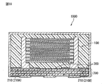
- the solid battery package of the present invention comprises a substrate, a solid battery provided thereon, and a water vapor barrier layer therebetween. That is, as shown in FIG. 2, the solid state battery package 1000 includes a substrate 200 to support the solid state battery 100, and the water vapor barrier layer 300 is provided between the solid state battery 100 and the substrate 200. . In such a solid state battery package, undesirable permeation of water vapor from the external environment through the substrate and into the solid state battery is reduced, thereby reducing or preventing deterioration of solid state battery characteristics over the long term.
- the substrate 200 is arranged close to one main surface side of the solid-state battery 100, and arranged so as to shield the main surface of the solid-state battery 100 from the external environment. Therefore, although it is generally considered that the presence of the substrate can prevent water vapor from penetrating into the solid-state battery, the inventors of the present application have focused on the fact that the substrate alone is not sufficient to prevent water vapor permeation. This is because, in the long term, the substrate may exhibit permeability to water vapor in the external environment due to the material and/or structure of the substrate. For this reason, in the present invention, the water vapor barrier layer 300 is provided between the solid battery 100 and the substrate 200 to effectively suppress water vapor permeation reaching the solid battery 100 through the substrate 200 . Therefore, for example, an undesirable event such as a decrease in the ionic conductivity of the solid electrolyte due to the reaction between water vapor (or moisture) entering from the substrate and the solid electrolyte can be suppressed or prevented.
- Water vapor as used herein is not particularly limited to water in a gaseous state, but also includes water in a liquid state.
- water vapor is used to broadly encompass items related to water regardless of its physical state. Therefore, “water vapor” can also be referred to as moisture, and in particular, water in a liquid state may include condensed water in which water in a gaseous state is condensed.
- the present invention is a packaged solid-state battery, and may have a structure that contributes to water vapor permeation prevention not only in the substrate but also in the whole.
- the solid state battery package of the present invention may be covered with a covering material to generally surround the solid state battery provided on the substrate. That is, the solid-state battery on the substrate may be packaged such that the side surfaces and main surface are surrounded by the covering material. With such a configuration, all the surfaces forming the solid-state battery are not exposed to the outside, and water vapor permeation can be more effectively prevented.
- the covering material may consist of a covering insulating layer and a covering inorganic film. That is, as shown in FIG. 2, the solid-state battery 100 provided on the substrate 200 may have a configuration in which the covering material 150 is covered with the covering insulating layer 160 and the covering inorganic layer 170 thereon.
- Covering insulating layer 160 is a layer provided to cover the main surface and side surfaces of solid-state battery 100 . As shown in FIG. 2, the insulating coating layer 160 is provided to cover at least the top surface 100A and the side surfaces 100B of the solid state battery 100, and the solid battery 100 on the substrate 200 is largely wrapped by the insulating coating layer 160 as a whole.
- the material of the insulating coating layer 160 may be of any type as long as it exhibits insulating properties.
- the insulating cover layer 160 may contain a resin (that is, may be a resin layer), and the resin may be either a thermosetting resin or a thermoplastic resin. That is, the coating material may be a resin layer (coating resin layer), and in a preferred embodiment, the coating material 150 may be composed of the resin layer (coating resin layer) 160 and the coating inorganic layer 170 provided thereon.
- the insulating cover layer 160 may contain an inorganic filler. Although this is merely an example, the insulating coating layer 160 may be made of an epoxy-based resin containing an inorganic filler such as SiC.
- the covering inorganic layer 170 is provided so as to cover the covering insulating layer 160 . As shown in FIG. 2 , the covering inorganic layer 170 is positioned on the covering insulating layer 160 , and thus has a shape that largely envelops the solid battery 100 on the substrate 200 as a whole together with the covering insulating layer 160 .
- the insulating coating layer 160 works together with the inorganic coating layer 170 to form a suitable water vapor barrier, and the inorganic coating layer 170 also works together with the insulating coating layer 160 to form a suitable water vapor barrier.
- the material of the coating inorganic layer 170 is not particularly limited, and may be metal, glass, oxide ceramics, or a mixture thereof.
- the covering inorganic layer 170 may be an inorganic film. That is, the covering inorganic layer 170 may correspond to an inorganic layer having a thin film form, such as a metal film. Although merely one example, the covering inorganic layer 170 may be formed of a Cu-based and/or Ni-based material having a thickness of 2 ⁇ m or more and 50 ⁇ m or less by plating.
- the substrate 200 may be a package member provided so as to support the solid-state battery 100 . That is, the substrate 200 provided closer to one main surface side (the main surface opposite to the main surface forming the top surface) of the solid-state battery 100 may serve as the support substrate. As shown in FIG. 2, the substrate 200 has a major surface larger than that of the solid-state battery 100, for example. Also, the substrate 200 may be a resin substrate. Alternatively, substrate 200 may be a ceramic substrate. In short, the substrate 200 may belong to a printed circuit board, a flexible substrate, an LTCC substrate, an HTCC substrate, or the like.
- the substrate 200 is preferably a member for external terminals of the packaged solid state battery. That is, the substrate 200 may serve as a terminal substrate for external terminals of the solid-state battery 100 .
- a solid-state battery package with such a substrate can mount the solid-state battery on another external substrate (ie, secondary substrate) such as a printed wiring board with the substrate interposed therebetween.
- the solid state battery can be surface mounted through the substrate through solder reflow or the like.
- the solid battery package of the present invention is preferably an SMD (SMD: Surface Mount Device) type battery package.
- the board preferably has wiring and/or electrode layers.
- the substrate may comprise electrode layers for electrical connection between the upper and lower major surfaces. That is, the substrate 200 according to a preferred embodiment includes electrode layers (upper main surface electrode layer 210, lower main surface electrode layer 220) that electrically connect the upper and lower main surfaces of the substrate, and is packaged. It is also a member for the external terminal of the solid-state battery (see Fig. 2).
- the electrode layer of the substrate and the terminal portion of the solid battery are connected to each other.
- the electrode layer of the substrate and the end face electrodes of the solid battery are electrically connected to each other.
- the positive electrode 140A of the solid battery is electrically connected to the positive electrode layer (210A, 220A) of the substrate, while the negative electrode 140B of the solid battery is connected to the negative electrode of the substrate. are electrically connected to the electrode layers (210B, 220B) of the .
- the electrode layers on the positive and negative sides of the substrate serve as the positive and negative terminals of the solid battery package, respectively.
- the solid-state battery package 1000 of the present invention has a configuration in which a water vapor barrier layer 300 is interposed between the solid-state battery 100 and the substrate 200 so as to favorably provide barrier properties that prevent moisture from penetrating into the solid-state battery (Fig. 2).
- the term “barrier” means having a property of preventing water vapor permeation such that water vapor in the external environment does not cause undesirable property deterioration of the solid-state battery.
- “barrier” as used herein means having a water vapor transmission rate of less than 5 ⁇ 10 ⁇ 3 g/(m 2 ⁇ Day).
- the water vapor barrier layer preferably has a water vapor transmission rate of 0 g/(m 2 ⁇ Day) or more and less than 5 ⁇ 10 ⁇ 3 g/(m 2 ⁇ Day) (for example, 0 .5 ⁇ 10 ⁇ 3 g/(m 2 ⁇ Day) or more and less than 5 ⁇ 10 ⁇ 3 g/(m 2 ⁇ Day)).
- water vapor transmission rate refers to the transmission rate obtained by the MA method under the measurement conditions of 85°C and 85% RH using a gas transmission rate measuring device of model WG-15S manufactured by MORESCO. pointing to
- the water vapor barrier layer 300 may be provided so as to be in contact with the covering insulation layer 160 . That is, the covering insulating layer 160 is preferably provided so as to cover not only the side surfaces of the solid battery 100 but also the bottom surface of the solid battery 100. The covering insulating layer 160 covering the side surfaces and/or the bottom surface of the solid battery 100 A water vapor barrier layer 300 may be provided so as to be in contact with the . This means that a water vapor barrier layer is provided between the sealing resin surrounding the solid-state battery and the substrate.
- the resist layer 400 is provided on the substrate 200 (a mode of providing the resist layer will be described later)
- the water vapor barrier layer 300 may be arranged between the insulating coating layer 160 and the resist layer 400 .
- the water vapor barrier layer is thinner than the layers forming the solid-state battery. That is, as shown in FIG. 3, the thickness of the water vapor barrier layer 300 located between the solid state battery 100 and the substrate 200 is equal to the thickness of the layers 110, 120, 130 (for example, at least one of them) forming the laminated structure of the solid state battery. may be smaller than the layer thickness of In other words, the water vapor barrier layer may be thinner than the positive electrode layer, thinner than the negative electrode layer, and/or thinner than the solid electrolyte layer. In another preferred embodiment, the water vapor barrier layer is thinner than the layers that make up the substrate. That is, as shown in FIG.
- the thickness of the water vapor barrier layer 300 positioned between the solid battery 100 and the substrate 200 is equal to the layer thickness of the layers 200′ (for example, at least one of them) forming the laminated structure of the substrate 200.
- the water vapor barrier layer may be thinner than the metal layer included in the substrate, and if the substrate is a resin substrate, it is smaller than the thickness of each resin layer that constitutes the substrate. It may be smaller than the layer thickness of each ceramic layer constituting the substrate.
- This relative thickness of the water vapor barrier layer relative to the various constituent layers of the solid state battery package prevents undesirable water vapor permeation in a design that is compatible with a low profile or compact solid state battery package. In other words, while preventing the permeation of water vapor, its influence on others is suppressed.
- the water vapor barrier layer may have, for example, a film form.
- the term “layers forming a laminated structure of a solid battery” as used herein broadly means a layer forming a battery structural unit of a solid battery, and narrowly means a positive electrode layer and a negative electrode layer. and any layer of the solid electrolyte layer between them.
- the water vapor barrier layer is thinner than the battery electrode layers, such as the positive and/or negative electrode layers of the solid state battery, and/or the water vapor barrier layer is thinner than the solid electrolyte layer of the solid state battery.
- the "layers constituting the substrate” referred to in this specification mean, for example, each layer assumed when constituting the substrate by lamination.
- a resin substrate as an example, macroscopically, when the substrate is configured by laminating a resin layer (for example, a layer made of a resin material impregnated into a base material such as glass fiber cloth) and a metal layer, the Each layer such as a resin layer and/or a metal layer corresponds to "a layer constituting a substrate".
- a resin substrate for example, a layer made of a resin material impregnated into a base material such as glass fiber cloth
- a metal layer corresponds to "a layer constituting a substrate".
- a ceramic substrate when the substrate is configured by laminating a ceramic layer and other metal layers macroscopically, each layer such as the ceramic layer and the metal layer corresponds to "a layer that constitutes the substrate”. do.
- the thickness for each layer of the water vapor barrier layer and the solid state battery and substrate may be based on electron microscopic images.
- the thickness of the water vapor barrier layer and the thickness of the layers composing the substrate and the solid-state battery are determined by cutting out a cross section with an ion milling device (manufactured by Hitachi High-Tech Co., model number IM4000PLUS) and scanning electron microscope (SEM) (manufactured by Hitachi High-Tech Co., Ltd. model number SU-). 8040). That is, the thickness dimension in this specification may refer to a value calculated from a dimension measured from an image acquired by such a method.
- the water vapor barrier layer may extend along the surface direction of the substrate.
- the water vapor barrier layer 300 may extend in the width direction of the solid state battery package 1000 and may extend across the solid state battery package.
- "extending in a direction along the surface direction” means extending in a direction parallel to the main surface of the substrate.
- the water vapor barrier layer extends in a direction orthogonal to the stacking direction of the solid-state battery.
- the water vapor barrier layer extends in all directions (all directions) perpendicular to the "stacking direction of the solid state battery".
- the water vapor barrier layer extending widely in the surface direction of the substrate in this manner can more preferably block water vapor entering from the external environment via the substrate.
- the water vapor barrier layer can be more preferably acted so that the water vapor that permeates from the outside of the package does not finally reach the solid-state battery. Solid state battery packages can be obtained.
- the water vapor barrier layer extending along the surface direction of the substrate is provided widely up to the region outside the solid-state battery.
- the water vapor barrier layer is provided widely so as to protrude from the installation area of the solid battery.
- the water vapor barrier layer may extend to the periphery of the solid state battery package, for example, the water vapor barrier layer may extend to the covering material covering the solid state battery. It can be said that the water vapor barrier layer may extend (in particular, extend in the surface direction of the substrate) so that the outer peripheral edge (preferably the entire outer peripheral edge) of the water vapor barrier layer reaches the outer peripheral edge of the solid battery package.
- the water vapor barrier layer may extend to the outer surface of the covering insulating layer that covers the solid battery on the substrate. That is, when the solid battery package 1000 has the insulating coating layer 160 provided on the substrate 200 to cover at least the top surface 100A and the side surfaces 100B of the solid battery 100, the insulating coating layer 160 covering the side surfaces 100B is Preferably, the water vapor barrier layer 300 extends to the outer surface 160A (see FIG. 4). This is because, as can be seen from the cross-sectional view of FIG. 4, water vapor entering from the external environment via the substrate 200 can be prevented more reliably.
- the water vapor barrier layer can more reliably act so that external water vapor that permeates through the substrate does not reach the solid-state battery, and the solid-state battery is more suitable for suppressing deterioration of solid-state battery characteristics over a long period of time.
- a battery package is provided.
- the water vapor barrier layer is an insulating film. That is, the water vapor barrier layer is an insulating film or insulating layer having electrical insulation.
- the water vapor barrier layer may be a film containing a material with high electrical insulation.
- insulation refers to the insulation properties of general insulators and therefore may have electrical resistivity . , preferably 1.0 ⁇ 10 6 ⁇ m or more, more preferably 1.0 ⁇ 10 7 ⁇ m or more (room temperature 20° C.). This is because an inconvenient event such as a short circuit can be further suppressed. In other words, it is possible to suitably suppress adverse electrical effects caused by the prevention of water vapor permeation.
- the film or layer of such a water vapor barrier is not particularly limited as long as it is a material exhibiting insulation properties, and specific examples of such materials include inorganic insulators such as glass and alumina, and organic insulators such as resins. These may be used singly or in combination of two or more.
- the water vapor barrier layer may be an inorganic film containing an inorganic material, and may be an insulating film exhibiting electrical insulation in terms of the inorganic material.
- the water vapor barrier layer may be an organic film containing an organic material, and may be an insulating film exhibiting electrical insulation in terms of the organic material.
- it may be a film in which such an inorganic material and an organic material are combined.
- the term "film” or "thin film” refers to a form having a small layer thickness, for example, having a "nanometer order thickness" (10 nm or more and 900 nm or less). can be interpreted as
- the water vapor barrier layer may have the form of a single layer.
- the water vapor barrier layer may have a multi-layer configuration (ie, a multi-layer configuration as described below). There is no particular limitation on their form, provided that they provide the desired moisture vapor permeation prevention properties.
- the water vapor barrier layer is an insulating multilayer film. Multilayering can improve the water vapor barrier properties of the water vapor barrier layer.
- the same film for example, a film made of the same material
- different films for example, films made of mutually different materials
- an organic insulating barrier layer may be formed on an inorganic insulating barrier layer.
- the water vapor barrier layer is provided so as to occupy substantially a large planar view area of the solid battery package. Specifically, the water vapor barrier layer is provided so as to occupy the entire area of the solid battery package in plan view, excluding the connection area (i.e., connection portion) between the end surface electrode of the solid battery and the electrode layer on the main surface of the substrate. It's okay to be Such a water vapor barrier layer having a large area in plan view can more reliably prevent water vapor from entering through the substrate from the external environment. Note that the water vapor barrier layer 300 of this aspect may extend at the height level of the joining member 600 provided between the end surface electrode and the electrode layer on the main surface of the substrate (see FIG. 4).
- the water vapor barrier layer 300 may extend across the joining member 600 in a cross-sectional view. In a cross-sectional view, water vapor barrier layer 300 may extend in contact with joining member 600 and may extend further outward until it contacts outer surface 160A of the covering insulating layer.
- the joint member 600 is responsible for at least electrical connection between the end surface electrodes of the solid-state battery and the substrate, and may contain, for example, a conductive adhesive (this is merely an example, but the joint member 600 is 600 may be composed of an epoxy-based conductive adhesive containing a metal filler such as Ag).
- the water vapor barrier layer is preferably a layer containing silicon. This is because it is likely to be a suitable layer in terms of electrical insulation.
- the water vapor barrier layer may be an inorganic layer or film containing silicon.
- the water vapor barrier layer containing silicon may be a layer composed of a molecular structure containing not only silicon atoms but also nitrogen atoms and/or oxygen atoms. This is because it tends to be a suitable layer in terms of electrical insulation and thinning.
- a water vapor barrier layer comprises both Si--O bonds and Si--N bonds. That is, both Si--O bonds and Si--N bonds may be present in the molecular structure constituting the layer material for the water vapor barrier layer.
- the layer tends to be thin and dense, and the water vapor barrier layer tends to exhibit more favorable properties of preventing water vapor permeation.
- the water vapor barrier layer is likely to be not only desirable in terms of electrical insulation and film thickness, but also exhibit more suitable water vapor permeation prevention properties. While this is desirable to prevent water vapor permeation, it does not have adverse effects (especially from the standpoint of lowering and/or miniaturizing solid-state battery packages and/or from an electrical standpoint). It means that it can be suppressed.
- water vapor barrier layer containing silicon and “water vapor barrier layer having both Si--O bonds and Si--N bonds” are not based on siloxane. That is, the water vapor barrier layer according to the present invention preferably has a molecular structure that contains silicon and Si—O bonds but does not contain a siloxane skeleton.
- Si--O bond and Si--N bond refer to those that can be confirmed based on Fourier transform infrared spectroscopy (FT-IR), for example. That is, in the water vapor barrier layer according to this aspect, Si—O bonds and Si—N bonds can be confirmed by measuring the absorption of light in the infrared region.
- FT-IR refers to measurement by a microscopic ATR method using, for example, Spotlight 150 manufactured by PerkinElmer.
- the water vapor barrier layer having Si—O bonds and Si—N bonds is, for example, a film thinner than each layer forming the laminated structure of the solid-state battery and/or each layer constituting the substrate. It is a thinner film than Therefore, it is possible to suitably prevent water vapor permeation with a design that does not go against the reduction in height or size of the solid battery package.
- the water vapor barrier layer having Si—O bonds and Si—N bonds preferably has a thickness on the order of nanometers, preferably 10 nm or more and 900 nm or less, more preferably 50 nm or more and 700 nm or less, still more preferably. is 50 nm or more and 500 nm or less, such as 50 nm or more and 400 nm or less, 50 nm or more and 300 nm or less, or 100 nm or more and 300 nm or less.
- a water vapor barrier layer having Si--O bonds and Si--N bonds can be a layer with relatively high toughness. This means that the water vapor barrier layer can act favorably during charging and discharging of the solid-state battery.
- the movement of ions between the positive and negative electrode layers through the solid electrolyte layer can cause the solid-state battery to expand and contract. Because of the layers, cracks and/or cracks are less likely to occur.
- a layer with high water vapor barrier properties is dense and hard and may have a tendency to crack and/or crack easily due to stress or the like, while it is relatively flexible without such cracks and/or cracks.
- the water vapor barrier layer containing Si—O bonds and Si—N bonds according to the present invention is less likely to crack or crack even when subjected to the stress of expansion and contraction due to the solid-state battery.
- the layer becomes highly permeable, and the reliability of the solid battery package becomes high.
- the water vapor barrier layer according to the present invention may contain, for example, SiON and/or SiNH sites in its molecular structure. That is, a water vapor barrier layer having Si--O bonds and Si--N bonds may contain SiON and/or SiNH. Also, the water vapor barrier layer having Si--O bonds and Si--N bonds may have different molecular or atomic concentrations along its thickness. For example, a relatively lower layer region may have more SiNH formed thereon, while a relatively upper layer region may have more SiON formed thereon. In other words, in the water vapor barrier layer provided between the substrate and the solid-state battery, the relatively upper layer region (that is, the side relatively close to the solid-state battery) has relatively Si—O bonds.
- the relatively lower layer regions may contain more Si—N bonds.
- the upper half region of the water vapor barrier layer (the upper half region relatively close to the solid-state battery) contains more Si—O bonds
- the lower half region of the water vapor barrier layer (the upper half region relatively close to the substrate) contains more Si—O bonds.
- lower half region may contain more Si—N bonds. That is, the H atom concentration is relatively high in the relatively lower layer region of the water vapor barrier layer, and the O atom concentration is relatively high in the relatively upper layer region of the water vapor barrier layer.
- a water vapor barrier layer (in particular, a water vapor barrier layer having Si—O bonds and Si—N bonds) is a layer containing both SiON sites and SiNH sites in its molecular structure. It's okay.
- a water vapor barrier layer containing both SiON and SiNH moieties is a dense layer and can be a layer with better water vapor permeation prevention properties.
- the water vapor barrier layer having Si--O bonds and Si--N bonds is formed from liquid raw materials. Specifically, it is preferable to form a water vapor barrier layer having both Si--O bonds and Si--N bonds by applying a liquid raw material to a substrate and irradiating it with light. As a result, the water vapor barrier layer can be formed without subjecting the substrate to higher temperatures, and adverse thermal effects on the substrate can be suppressed.
- the vacuum deposition method and the like generally require an expensive deposition apparatus, but formation using such a liquid source does not require such an expensive apparatus, and the cost can be kept relatively low.
- the layer formed from the liquid raw material as described above has little or substantially no stress. typically no such stress occurs. Therefore, the risk of the substrate warping when manufacturing the water vapor barrier layer from the liquid raw material is reduced or prevented.
- the solid battery package of the present invention can be embodied in various ways. For example, the following aspects are conceivable.
- This aspect has a form in which a resist layer is arranged between the substrate and the solid-state battery.
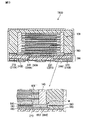
- solid state battery package 1000 may have a resist layer 400 between substrate 200 and solid state battery 100 (see FIG. 5).
- the resist layer 400 is particularly provided on the main surface of the substrate 200 .
- a resist layer is a layer that at least partially covers the substrate surface to protect it from physical processing or chemical reaction. Therefore, the resist layer may be an insulating layer containing a resin material provided on the main surface of the substrate 200 .
- Such a resist layer can also be regarded as equivalent to a heat-resistant coating provided on the main surface of substrate 200 .
- it may be a resist that maintains insulation when connecting the solid battery and the substrate and serves to protect the conductor portion such as the electrode layer of the substrate.
- the resist layer 400 provided on the main surface of the substrate 200 may be a so-called "solder resist" layer.
- the water vapor barrier layer may have higher barrier properties than the resist layer.
- the water vapor barrier layer 300 preferably has a lower water vapor transmission rate than the resist layer 400 .
- a resist layer made of solder resist is not necessarily sufficient in terms of preventing water vapor permeation, it can more preferably block water vapor entering from the external environment through the substrate.
- the resist layer is composed of a solder resist containing resin such as epoxy and/or acrylic, the resist layer can correspond to an insulating layer having a water vapor transmission rate of 1 g/(m 2 ⁇ Day) or more.
- the water vapor barrier layer may have a water vapor transmission rate lower than that of such an insulating layer (that is, a water vapor transmission rate of 0 g/(m 2 ⁇ Day) or more and less than 1 g/(m 2 ⁇ Day), for example). .
- a resist layer 400 may be provided on the main surface of the substrate 200 (in particular, the main surface on the side relatively close to the solid-state battery 100).
- the water vapor barrier layer 300 may be disposed at least on the resist layer 400 .
- the water vapor barrier layer 300 is arranged in direct contact with the resist layer 400 so that the water vapor barrier layer 300 and the resist layer 400 are stacked on each other.
- the water vapor barrier layer may also be partially provided on the substrate surface.
- the water vapor barrier layer 300 on the resist layer 400 may also be partially positioned on the substrate 200 (in FIG. 5, a water vapor barrier layer located on the substrate 200). A portion of the layer is shown as 310). That is, in a cross-sectional view, the water vapor barrier layer overlapping the resist layer in the stacking direction may extend beyond the resist layer so as to be partially aligned with the resist layer.
- the water vapor barrier layer is also partially positioned on the substrate in this manner, the water vapor barrier properties of the solid state battery package can be improved.
- the electrode layer of the substrate made of a metal with a high water vapor barrier property, the substrate resin portion with a low water vapor barrier property, and the interface can be more reliably covered with the water vapor barrier layer.
- the water vapor barrier properties of the solid state battery package can be improved. From this point of view, the water vapor barrier layer provided so as to overlap the resist layer may be positioned at least partially on the electrode of the substrate.
- the substrate has a metal layer as its moisture permeation retarding structure. That is, the substrate itself of the solid battery package has a structure that contributes to preventing water vapor permeation.
- a metal layer 240 is included as a layer constituting the substrate 200, and the outer contour of the substrate 200 in plan view and the outer contour of the metal layer 240 in plan view overlap (FIG. 6). and FIG. 7). That is, the metal layer 240 extends over a large area to the periphery of the substrate 200 .
- the substrate is a resin substrate, it can be said that the metal layer extends to a position exposed to the outer periphery (outermost periphery) of the resin substrate.
- the metal layer is denser than the resin portion and/or the ceramic portion and contributes to preventing water vapor permeation. Therefore, water vapor entering from the external environment can be prevented in advance at the substrate. In other words, combined with the effect of the water vapor barrier layer, the effect of preventing the infiltration of external water vapor through the substrate from reaching the solid-state battery becomes more reliable.
- a solid state battery package is provided. For example, if the substrate has a metal layer that contributes to moisture transmission retardation, the solid battery package can have a water vapor barrier property with a water vapor transmission rate of less than 2.5 ⁇ 10 ⁇ 3 g/(m 2 ⁇ Day) (this lower limit can be 0 g/(m 2 ⁇ Day).
- the metal layer may be, for example, a layer made of at least one metal material selected from the group consisting of copper, aluminum, stainless steel, nickel, silver, gold and tin.
- the metal layer may be a metal foil, for example a copper foil.
- the metal layer may correspond to a layer located inside the substrate. That is, the substrate has a first electrode layer for electrical connection with the solid battery on one main surface and a second electrode layer for mounting the solid battery package on the external substrate on the other main surface. If present, a metal layer may be positioned between the first electrode layer and the second electrode layer. For example, a metal layer in the substrate inner region between the first electrode layer 210 corresponding to the mounting layer of the solid battery 100 and the second electrode layer 220 (for example, the second electrode layer 220 corresponding to the so-called customer mounting layer) 240 may be provided (see FIG. 6). In this way, the metal layer can be provided exclusively for preventing water vapor permeation separately from the electrode layer, so that the substrate can more effectively prevent water vapor permeation.
- the metal layer may or may not be responsible for electrical connection between the upper and lower main surfaces of the substrate.
- the metal layer 240 corresponds to a non-electrically connecting metal layer provided in the substrate inner region. That is, the metal layer 240 in such a case is not electrically connected to the first electrode layer 210 and the second electrode layer 220 .
- the metal layer 240 corresponds to a metal layer for electrical connection provided in the inner region of the substrate when it is responsible for electrical connection between the upper and lower main surfaces of the substrate. That is, the metal layer 240 in such a case is electrically connected to the first electrode layer 210 and the second electrode layer 220 .
- the metal layer may be a dummy electrode layer that does not provide electrical connection between the upper and lower principal surfaces. That is, it may be a metal layer that is not electrically connected to the first electrode layer and the second electrode layer and is provided exclusively for preventing water vapor permeation.
- the metal layer may be a ground layer. That is, a metal layer for preventing water vapor permeation may be used as the ground layer.
- Such a water vapor permeation blocking metal layer may be a single layer, but is not necessarily limited to this.
- the metal layer may be provided as at least two layers on the substrate if more emphasis is placed on increasing the effect of preventing water vapor permeation. As shown in FIG.
- the substrate base material layer 250 such as a resin layer has a meandering shape when viewed in cross section.
- the water vapor entry path of the substrate becomes a detour, and water vapor permeation to the solid-state battery can be more preferably prevented.
- the metal layer extending across the substrate has a configuration that occupies substantially the entire planar level of the substrate. It can be said that the metal layer provided inside the substrate and extending in the plane direction of the substrate occupies substantially the entire substrate surface (virtual plane inside the substrate) at such an extension level.
- the area of the metal layer 240 in plan view is 90% or more, preferably 95% or more, more preferably 99% or more of the area of the substrate 200 in plan view. That is, the metal area ratio in the substrate may be 90% or more, preferably 95% or more, more preferably 99% or more.
- the upper limit of such area ratio may be 100% (other area ratios/occupancy ratios, etc. referred to herein may also have an upper limit of 100%).
- such a metal area ratio may include a metal portion (for example, a via) in an opening of a metal layer, which will be described later.
- the area of the planar view shape of the metal layer 240 is 90% or more and 99.5% or less, 95% or more and 99.5% or less, etc. with respect to the planar view shape area of the substrate 200.
- the substrate surface occupancy of the metal layer extending in the substrate surface direction inside the substrate may be 90% or more, preferably 95% or more, and more preferably 99% or more. This means that the plan view shape of the metal layer 240 and the plan view shape of the substrate 200 are substantially the same when viewed macroscopically (see FIG. 7). It becomes possible to more reliably block the coming water vapor at the substrate portion.
- the metal layer provided as the moisture permeation retardation structure of the substrate has a unique opening shape.
- the planar view shape of the opening region provided in the metal layer is circular.
- the metal layer 240 that extends widely to the periphery of the substrate 200 may have an opening region 245 that has a circular plan view shape (or a plan view outline of the opening).
- a circular shape in a plan view has little shape anisotropy and tends to contribute to an improvement in the metal area ratio.
- such an opening can improve the metal area ratio of the substrate in plan view, and can further enhance the effect of preventing water vapor permeation. Therefore, it is easy to obtain a long-life solid-state battery package in which the deterioration of the solid-state battery characteristics is more suitably suppressed in the long term.
- planar view shape of the opening region for the via that is responsible for the electrical connection between the upper and lower main surfaces may be circular.
- the metal portion or the conductive portion that joins the upper and lower layers of the substrate preferably has a circular shape (circular in a plan view).
- the term "circular” is not limited to a perfect circular shape (i.e., simply “circle” or “perfect circle”), but is usually included in “round shape” as recognized by those skilled in the art, although it may vary from that. It also includes the generally circular shape obtained. For example, not only a circle or a perfect circle, but also a shape whose arc has a locally different curvature, or a shape derived from a circle or a perfect circle, such as an ellipse, may be used.
- metal area ratio may be considered to include the metal area of the via portion.
- a metal layer having an opening region has a planar area of the metal layer including the area of the via located in the opening region (the area of the planar shape of the via on the same plane as the metal layer). , 90% or more, preferably 95% or more, more preferably 99% or more.
- the substrate is particularly a resin substrate. That is, the solid battery package includes a substrate containing resin as a base material.
- the laminate structure of the substrate may include a resin layer.
- the resin material of such resin layers may be any thermoplastic and/or any thermosetting resin.
- the resin layer may be formed by impregnating a fiber cloth and/or paper as a base material with a resin material. For example, it may be made by impregnating a glass fiber cloth with a resin material such as an epoxy resin.
- the resin substrate can act favorably during charging and discharging of the solid battery.
- the solid battery may expand and contract due to movement of ions between the positive and negative electrode layers through the solid electrolyte layer.
- the load on the layers can be reduced. In other words, the risk of damaging the water vapor barrier layer during use of the solid battery package is reduced, and the reliability of the package can be improved in terms of preventing water vapor permeation.
- the resin exhibits considerable permeability to water vapor (for example, various forms of water vapor including water vapor in the air).
- the inventors of the present application have found that there is a possibility that it will be lost. Therefore, when the substrate is a resin substrate, the effect of the substrate metal layer for retarding moisture permeation, that is, the effect of the metal layer that more reliably blocks water vapor from the external environment at the substrate portion, etc., tends to become apparent.
- the package product of the present invention is obtained by preparing a solid battery containing a battery structural unit having a positive electrode layer, a negative electrode layer, and a solid electrolyte between the electrodes, and then packaging the solid battery. be able to.
- the production of the solid-state battery package of the present invention can be broadly divided into the production of the solid-state battery itself (hereinafter also referred to as the "pre-packaged battery"), which corresponds to the pre-packaging stage, the preparation of the substrate, and the packaging. can.
- the prepackaged battery can be manufactured by a printing method such as a screen printing method, a green sheet method using a green sheet, or a combination thereof. That is, the pre-packaged battery itself may be produced according to a conventional solid-state battery production method (thus, solid electrolytes, organic binders, solvents, optional additives, positive electrode active materials, negative electrode active materials, etc. described below). may be those used in the manufacture of known solid-state batteries).
- a slurry is prepared by mixing a solid electrolyte, an organic binder, a solvent and optional additives.
- a sheet comprising a solid electrolyte is then formed from the prepared slurry by sintering.
- a positive electrode paste is prepared by mixing a positive electrode active material, a solid electrolyte, a conductive material, an organic binder, a solvent and optional additives.
- a negative electrode paste is prepared by mixing a negative electrode active material, a solid electrolyte, a conductive material, an organic binder, a solvent and optional additives.
- a negative electrode paste is printed on the sheet, and a current collection layer and/or a negative layer are printed as necessary.
- a laminate is obtained by alternately laminating a sheet printed with the positive electrode paste and a sheet printed with the negative electrode paste.
- the outermost layer (uppermost layer and/or lowermost layer) of the laminate may be an electrolyte layer, an insulating layer, or an electrode layer.
- the laminate is integrated by pressure bonding, it is cut into a predetermined size.
- the obtained cut laminate is subjected to degreasing and firing.
- a fired laminate is thus obtained.
- the laminate may be subjected to degreasing and baking before cutting, and then cutting may be performed.
- the end surface electrode on the positive electrode side can be formed by applying a conductive paste to the side surface of the fired laminate where the positive electrode is exposed.
- the end surface electrode on the negative electrode side can be formed by applying a conductive paste to the negative electrode exposed side surface of the fired laminate.
- the end surface electrodes on the positive electrode side and the negative electrode side may be provided so as to reach the main surface of the fired laminate. This is because it can be connected to the main surface electrode layer of the substrate in the next step in a small area (more specifically, the end surface electrode provided so as to extend to the main surface of the fired laminate has a folded portion on the main surface. but such folded portions can be electrically connected to the major surface electrode layer of the substrate).
- a component of the end face electrode can be selected from at least one selected from silver, gold, platinum, aluminum, copper, tin and nickel.
- end surface electrodes on the positive electrode side and the negative electrode side are not limited to being formed after firing the laminate, and may be formed before firing and subjected to simultaneous firing.
- a desired prepackaged battery can be finally obtained by going through the steps described above.
- the substrate is a resin substrate
- its preparation may be carried out by laminating a plurality of layers and subjecting them to heat and pressure treatment.
- at least one resin sheet formed by impregnating a resin raw material into a base material such as fiber cloth and/or paper, and at least one metal sheet (for example, a sheet of metal foil) are prepared, and these are placed together. Overlap to form a substrate precursor.
- a resin substrate can be obtained by subjecting the substrate precursor to heat and pressure using a press.
- the main surface electrode layer provided on the main surface of the substrate to be electrically connected may be appropriately patterned.
- a sheet having a desired shape may be included as the metal sheet.
- a metal sheet including at least a sheet for retarding moisture permeation is alternately laminated with the resin sheet to form a substrate precursor, and the resin substrate is provided with a metal layer for retarding moisture permeation by subjecting it to heat and pressure treatment. can be obtained.
- ceramic substrate When the substrate is a ceramic substrate, its preparation may be carried out, for example, by laminating and firing a plurality of green sheets.
- a semi-rack substrate may have vias and/or lands.
- holes are formed in the green sheet by a punch press or a carbon dioxide gas laser, and the holes are filled with a conductive paste material.
- Precursors of metal or conductive portions such as wiring layers and/or electrode layers may be formed.
- the ceramic substrate preferably comprises a non-connected metal layer with no electrical connection as a water vapor permeation blocking layer.
- the metal layer (particularly its precursor) may be formed on the green sheet.
- Such a metal layer may be formed by a printing method, or may be formed by arranging a metal foil or the like. Next, a predetermined number of such green sheets are stacked and thermally compressed to form a green sheet laminate, and the green sheet laminate is fired to obtain a ceramic substrate.
- the land and the like can also be formed after firing the green sheet laminate.
- a desired substrate can be finally obtained through the above steps.
- a water vapor barrier layer may be formed on the substrate. That is, the water vapor barrier may be formed on the substrate prior to packaging the substrate and solid state battery together.
- the water vapor barrier layer is not particularly limited as long as the desired barrier layer can be formed.
- a "water vapor barrier layer having Si--O bonds and Si--N bonds” can be formed by applying a liquid raw material and irradiating ultraviolet rays.
- a precursor layer obtained by coating a liquid raw material containing a silicon compound, such as a silicon compound containing a Si—N—Si bond and a solvent (for example, an organic solvent) is irradiated with ultraviolet light.
- a "water vapor barrier layer having Si--O bonds and Si--N bonds” can be obtained.
- the water vapor barrier layer is formed from a liquid raw material under relatively low temperature conditions (for example, temperature conditions of about 100° C.) without using a vapor deposition method such as CVD or PVD.
- a raw material containing a silicon compound such as silazane is prepared as a liquid raw material, and the liquid raw material is applied to a substrate by spin coating or spray coating and dried to form a barrier precursor. Then, by subjecting the barrier precursor to UV irradiation in an atmosphere containing nitrogen and/or oxygen, a "water vapor barrier layer having Si--O bonds and Si--N bonds" can be obtained.
- a layer" can be obtained by subjecting a barrier precursor layer comprising a silicon compound (eg silazane) containing Si--N--Si bonds to UV irradiation in an ambient atmosphere containing nitrogen and oxygen.
- a barrier precursor layer comprising a silicon compound (eg silazane) containing Si--N--Si bonds
- active oxygen is generated in the surrounding atmosphere by the UV irradiation, and the active oxygen penetrates from the outer surface of the barrier precursor layer to obtain the water vapor barrier layer.
- UV irradiation is performed to generate active oxygen in an ambient atmosphere containing oxygen and nitrogen, and to promote the breaking of molecular bonds of "silicon compounds containing Si—N—Si bonds" in the barrier precursor layer.
- the outer surface of the barrier precursor layer and the nearby inner layer region contain relatively many Si—O bonds, while the inner layer region relatively distal to the outer surface of the barrier precursor layer contains Since the effect of UV irradiation is relatively small and the breakage of the molecular bonds is less likely to be promoted, the Si—N bonds are relatively abundant.
- the layer region relatively close to the solid-state battery contains relatively many Si—O bonds, while the layer region relatively close to the substrate A water vapor barrier layer containing a relatively large number of Si—N bonds can be obtained.
- the water vapor barrier layer When forming the water vapor barrier layer, it is preferable to locally remove the barrier layer so that the water vapor barrier layer does not exist at the junction between the conductive portion of the substrate and the end face electrode of the solid-state battery.
- a mask may be utilized so that the water vapor barrier layer is not formed only at the junction. In other words, a mask may be applied to the regions to be joined, the water vapor barrier layer may be formed on the entire surface, and then the mask may be removed.
- a water vapor barrier layer 300 may be formed on the resist layer 400 as shown in FIGS. 9(A) and 9(B). At this time, as described above, it is preferable to form the water vapor barrier layer 300 so as to exclude the bonding region 500 with the solid battery 100 . That is, it is preferable to prepare the substrate 200 on which the resist layer 400 and the water vapor barrier layer 300 are formed so that the surface electrodes of the substrate are exposed. In addition, if necessary, a water vapor barrier layer may be formed on the resist layer so that a part of the water vapor barrier layer is positioned on the surface electrode of the substrate.
- the pre-packaged battery 100 is placed on the substrate 200 . That is, an "unpackaged solid battery” is placed on the substrate (hereinafter, the battery used for packaging is also simply referred to as a "solid battery”).
- the solid state battery is arranged on the substrate such that the conductive portion of the substrate and the end face electrodes of the solid state battery are electrically connected to each other.
- a conductive paste may be provided on the substrate (particularly for the "junction" areas described above), thereby electrically connecting the conductive portions of the substrate and the end-face electrodes of the solid-state battery to each other. You can connect. More specifically, the electrode layer on the main surface of the substrate and the folded portion of the end surface electrode on the positive electrode side of the solid battery are aligned, and the other electrode layer on the main surface of the substrate and the folded portion of the end surface electrode on the negative electrode side of the solid battery are aligned.
- a conductive paste for example, Ag conductive paste
- the precursor 600 ′ of the bonding member that is responsible for electrical connection between the solid-state battery 100 and the substrate 200 may be provided in advance.
- a bonding member precursor 600′ can be provided by printing a conductive paste that does not require washing such as flux after formation, such as Ag conductive paste, nanopaste, alloy paste, brazing material, etc. can.
- the solid battery 100 is placed on the substrate so that the end surface electrode of the solid battery and the precursor 600′ of the bonding member are in contact with each other, and the precursor 600′ is heated to separate the solid battery 100 and the substrate 200 from the precursor 600′.
- a joint member 600 contributing to electrical connection between them is formed.
- a covering material is formed. As shown in FIG. 9(E), as the covering material 150, a covering insulating layer 160 and a covering inorganic layer 170 may be provided.
- a covering insulating layer 160 is formed so as to cover the solid battery 100 on the substrate 200 . Therefore, the material for the covering insulating layer 160 is provided so as to completely cover the solid state battery on the substrate.
- the insulating coating layer is made of a resin material
- a resin precursor is provided on the substrate and subjected to curing or the like to form the insulating coating layer.
- the covering insulating layer may be molded through application of pressure with a mold.
- an overlying insulating layer may be molded through compression molding to encapsulate the solid state battery on the substrate.
- the raw material for the insulating coating layer may be in the form of granules, and may be of thermoplastic type.
- Such molding is not limited to mold molding, and may be performed through polishing, laser processing and/or chemical treatment.
- the covering inorganic layer 170 is formed. Specifically, the covering inorganic layer 170 is formed on the “covering precursor in which the individual solid-state batteries 100 are covered with the covering insulating layer 160 on the support substrate 200”. For example, a plating layer is formed. As an example only, dry plating may be performed to provide a dry plating film as the coating inorganic layer.
- the present invention is not particularly limited to this.
- no resist layer may be provided between the substrate 200 and the solid-state battery 100 (see FIG. 10). That is, for example, the resist layer 400 described with reference to FIG. 5 may not be provided.
- the water vapor barrier 300 is formed from the base material portion (eg, resin portion or ceramic portion) on the substrate and/or the electrode layer on the substrate surface. 210 (positive electrode layer 210A and/or negative electrode layer 210B).
- the present invention may have a form in which the solid-state battery 100 is largely covered with the covering material 150 .
- the covering inorganic layer 170 provided on the covering insulating layer 160 covering the solid battery 100 on the substrate 200 may extend to the lower main surface of the substrate 200 (see FIG. 2). That is, the covering inorganic layer 170 on the covering insulating layer 160 as the covering material 150 extends to the side surface of the substrate 200 and beyond the side surface to the lower main surface of the substrate 200 (particularly its peripheral portion). May be extended.
- the coating inorganic layer 170 can also be provided as a multi-layer structure consisting of at least two layers.
- FIG. 11 shows the covering inorganic layer 170 having a two-layer structure of 170A and 170B.
- Such a multilayer structure is not limited to between different materials, but may be between same materials. The provision of such a multi-layer structure of the covering inorganic layer may improve the water vapor barrier properties of the entire package.
- the water vapor barrier layer may extend up to or in contact with the covering inorganic layer.
- the water vapor barrier layer 300 may extend up to or against the covering inorganic layer 170 covering the sides of the solid state battery 100 (see FIGS. 2 and 11). This is because, as can be seen from the cross-sectional views of FIGS. 2 and 11, water vapor entering from the external environment via the substrate 200 can be more reliably blocked.
- the water vapor barrier layer 300 may extend up to .
- the water vapor barrier layer can more reliably act so that external water vapor that permeates through the substrate does not reach the solid-state battery, and the deterioration of solid-state battery characteristics is suppressed in the long term.
- a solid state battery package is provided.
- the vapor barrier layer 300 extending to the outer surface or the outer surface of the insulating coating layer 160 may be in contact with the inorganic coating layer 170 . I can say.
- a metal layer having a high "metal area ratio” was mentioned, but the present invention may achieve a high metal area ratio from a plurality of substrate metal layers.
- a plurality of metal layers for example, metal layers provided as metal layer 240A, metal layer 240B, and metal layer 240C, have a metal area ratio of 90% or more, preferably 95% or more, and more Preferably, a metal area percentage of 99% or more may be achieved. This is an area ratio of 90% or more, preferably 95% or more, more preferably 99% or more of the total area of the planar shapes of the metal layers 240A, 240B, and 240C (of the substrate 200).
- the target metal layer may more preferably have a metal area ratio of 99% or more in total in plan view.
- a plurality of metal layers eg, metal layer 240A, metal layer 240B, and metal layer 240C
- metal layer 240A, metal layer 240B, and metal layer 240C are positioned on different planes (in short, different height levels or depth levels) within the substrate. and/or may not overlap each other in a top perspective view of the substrate.
- the via in the opening region of the metal layer was mentioned, but it can also be understood that the metal layer or metal portion connecting the first electrode layer and the second electrode layer has a via structure. That is, the substrate may be provided with a metal structure or metal portion that communicates with one or more layers when viewed in cross section. Considering these matters, the substrate according to the present invention can be expressed in various metal layer forms. For example, in a substrate, a first electrode layer (an electrode layer for electrical connection with a solid-state battery on one main surface of the substrate) and a second electrode layer (an external substrate of a solid-state battery package on the other main surface of the substrate) and the substrate may further have a second metal layer that is not connected to the first electrode layer and the second electrode layer.
- the first metal layer may preferably correspond to a metal layer (or a metal part, eg a via part) electrically connecting the first electrode layer and the second electrode layer to each other.
- the substrate comprises, between the first electrode layer and the second electrode layer, a first metal layer (or a metal portion, e.g. a via portion) electrically connected to the first electrode layer and the second electrode layer. and a second metal layer that is not electrically connected to the first electrode layer and the second electrode layer.
- the first metal layer and the second metal layer may be made of the same metal material, or may be made of different metal materials.
- the package substrate serves as a terminal substrate for the external terminals of the solid-state battery
- permeation of water vapor from the external environment to the solid-state battery can be preferably prevented in the solid-state battery package.
- a first metal layer and a second metal layer may be positioned on the same plane (in short, the same height level or depth level) within the substrate, or may be positioned on different planes ( In short, they may be positioned at different height levels or depth levels).
- the area of the shape in plan view of the first metal layer and the second metal layer may be, for example, 90% or more of the area of the shape in plan view of the substrate.
- the total area of the plan view shape of the first metal layer and the plan view shape of the second metal layer is preferably 90% or more, and more preferably, the area of the plan view shape of the substrate. is 95% or more, more preferably 99% or more (the upper limit of such area ratio may be 100%).
- the upper limit of such area ratio may be 100%.
- the conductive paste provided on the substrate is used to electrically connect the conductive portion of the substrate and the end surface electrode of the solid-state battery to each other. It may finally have a form as shown in 13.
- the pressing force is applied from the solid battery 100 to the conductive paste 600 ′, so that the end surface electrode 140 of the solid battery 100 is apt to slightly bite into the conductive paste 600'. That is, the conductive paste 600' is pressed against the end face electrode 140 and tends to have a slightly protruding shape ("M" portion in FIG. 13) on the outer side thereof.
- the conductive paste 600′ is partially pressed to form a resist layer. It can flow over 400. That is, the conductive paste 600′ is positioned on the main surface electrode layer 210 of the substrate inside the resist layer 400 and the water vapor barrier layer 300 as shown in FIG. It will extend over the barrier layer 300 . This is related to the resist layer 400 and water vapor barrier layer 300 acting as a "dam" for the conductive paste 600'. More specifically, the opening portions of the resist layer 400 and the water vapor barrier layer 300 that expose the conductive portion of the substrate (especially the main surface electrode layer 210 of the substrate) are coated with the conductive paste 600 at the edges forming the opening.
- the conductive paste 600' once applied to the opening part flows onto the water vapor barrier layer 300 as the pressure is applied, while the conductive paste 600' Most of 600 ′ can remain in the openings of resist layer 400 and water vapor barrier layer 300 . That is, the resist layer (for example, solder resist layer) and the water vapor barrier layer thereon preferably act as a dam to suppress bleeding of the conductive paste.
- the bonding area between the water vapor barrier layer 300 and the insulating coating layer 160 is more likely to be secured. The sticking force between them can be more stable.
- the conductive paste 600 ′ is an expression based on the premise of manufacturing, but in terms of the solid battery after manufacturing, the conductive paste 600 ′ corresponds to the bonding member 600 . Therefore, in the solid battery package 1000 according to an embodiment of the present disclosure, as shown in FIG. 13, the bonding member 600 is positioned inside the resist layer 400 and the water vapor barrier layer 300 (especially on the upper main surface electrode layer 210 of the substrate). area), part of which extends over the water vapor barrier layer 300 .
- such a package may be provided as an electronic device mounted on an external substrate separate from its substrate.
- the substrate of the solid battery package can serve as a terminal substrate for the external terminals of the solid battery.
- a solid state battery package may be provided for such an electronic device.
- the solid battery package of the present invention can be used in various fields where battery use or power storage is assumed. Although it is only an example, the solid battery package of the present invention can be used in the electric, information, and communication fields where mobile devices are used (for example, mobile phones, smartphones, laptop computers and digital cameras, activity meters, arm computers, electronic devices, etc.). Paper, RFID tags, card-type electronic money, electric and electronic equipment fields including small electronic devices such as smart watches, or mobile equipment fields), household and small industrial applications (for example, power tools, golf carts, household / Nursing care and industrial robots), large industrial applications (e.g. forklifts, elevators, harbor cranes), transportation systems (e.g.
- hybrid vehicles electric vehicles, buses, trains, electrically assisted bicycles, electric motorcycles, etc.
- power system applications e.g., various power generation, load conditioners, smart grids, general household electrical storage systems, etc.
- medical applications medical equipment such as earphone hearing aids
- pharmaceutical applications medication management systems, etc.
- IoT field space/deep sea applications (for example, fields such as space probes and submersible research vessels).
Landscapes
- Chemical & Material Sciences (AREA)
- Chemical Kinetics & Catalysis (AREA)
- Electrochemistry (AREA)
- General Chemical & Material Sciences (AREA)
- Inorganic Chemistry (AREA)
- Engineering & Computer Science (AREA)
- Manufacturing & Machinery (AREA)
- Physics & Mathematics (AREA)
- Condensed Matter Physics & Semiconductors (AREA)
- General Physics & Mathematics (AREA)
- Secondary Cells (AREA)
- Sealing Battery Cases Or Jackets (AREA)
Priority Applications (3)
| Application Number | Priority Date | Filing Date | Title |
|---|---|---|---|
| CN202280030985.5A CN117203825A (zh) | 2021-04-26 | 2022-04-26 | 固体电池封装体 |
| JP2023517574A JP7626208B2 (ja) | 2021-04-26 | 2022-04-26 | 固体電池パッケージ |
| US18/487,403 US20240047793A1 (en) | 2021-04-26 | 2023-10-16 | Solid-state battery package |
Applications Claiming Priority (2)
| Application Number | Priority Date | Filing Date | Title |
|---|---|---|---|
| JP2021074349 | 2021-04-26 | ||
| JP2021-074349 | 2021-04-26 |
Related Child Applications (1)
| Application Number | Title | Priority Date | Filing Date |
|---|---|---|---|
| US18/487,403 Continuation US20240047793A1 (en) | 2021-04-26 | 2023-10-16 | Solid-state battery package |
Publications (1)
| Publication Number | Publication Date |
|---|---|
| WO2022230900A1 true WO2022230900A1 (ja) | 2022-11-03 |
Family
ID=83848458
Family Applications (1)
| Application Number | Title | Priority Date | Filing Date |
|---|---|---|---|
| PCT/JP2022/018942 Ceased WO2022230900A1 (ja) | 2021-04-26 | 2022-04-26 | 固体電池パッケージ |
Country Status (4)
| Country | Link |
|---|---|
| US (1) | US20240047793A1 (https=) |
| JP (1) | JP7626208B2 (https=) |
| CN (1) | CN117203825A (https=) |
| WO (1) | WO2022230900A1 (https=) |
Cited By (1)
| Publication number | Priority date | Publication date | Assignee | Title |
|---|---|---|---|---|
| JPWO2022230901A1 (https=) * | 2021-04-26 | 2022-11-03 |
Citations (4)
| Publication number | Priority date | Publication date | Assignee | Title |
|---|---|---|---|---|
| JP2015220107A (ja) * | 2014-05-19 | 2015-12-07 | Tdk株式会社 | 全固体リチウムイオン二次電池 |
| JP2017182945A (ja) * | 2016-03-29 | 2017-10-05 | Tdk株式会社 | 全固体リチウムイオン二次電池 |
| WO2019164006A1 (ja) * | 2018-02-26 | 2019-08-29 | 株式会社村田製作所 | 全固体電池 |
| WO2020203879A1 (ja) * | 2019-03-29 | 2020-10-08 | 株式会社村田製作所 | 固体電池 |
Family Cites Families (3)
| Publication number | Priority date | Publication date | Assignee | Title |
|---|---|---|---|---|
| JP5164369B2 (ja) * | 2006-12-08 | 2013-03-21 | 日本合成化学工業株式会社 | 二次電池 |
| JP2018186001A (ja) * | 2017-04-26 | 2018-11-22 | 昭和電工株式会社 | リチウムイオン二次電池 |
| CN112567562B (zh) * | 2018-08-10 | 2023-12-05 | 株式会社村田制作所 | 固态电池 |
-
2022
- 2022-04-26 WO PCT/JP2022/018942 patent/WO2022230900A1/ja not_active Ceased
- 2022-04-26 CN CN202280030985.5A patent/CN117203825A/zh active Pending
- 2022-04-26 JP JP2023517574A patent/JP7626208B2/ja active Active
-
2023
- 2023-10-16 US US18/487,403 patent/US20240047793A1/en active Pending
Patent Citations (4)
| Publication number | Priority date | Publication date | Assignee | Title |
|---|---|---|---|---|
| JP2015220107A (ja) * | 2014-05-19 | 2015-12-07 | Tdk株式会社 | 全固体リチウムイオン二次電池 |
| JP2017182945A (ja) * | 2016-03-29 | 2017-10-05 | Tdk株式会社 | 全固体リチウムイオン二次電池 |
| WO2019164006A1 (ja) * | 2018-02-26 | 2019-08-29 | 株式会社村田製作所 | 全固体電池 |
| WO2020203879A1 (ja) * | 2019-03-29 | 2020-10-08 | 株式会社村田製作所 | 固体電池 |
Cited By (2)
| Publication number | Priority date | Publication date | Assignee | Title |
|---|---|---|---|---|
| JPWO2022230901A1 (https=) * | 2021-04-26 | 2022-11-03 | ||
| JP7639898B2 (ja) | 2021-04-26 | 2025-03-05 | 株式会社村田製作所 | 固体電池パッケージ |
Also Published As
| Publication number | Publication date |
|---|---|
| JP7626208B2 (ja) | 2025-02-04 |
| CN117203825A (zh) | 2023-12-08 |
| JPWO2022230900A1 (https=) | 2022-11-03 |
| US20240047793A1 (en) | 2024-02-08 |
Similar Documents
| Publication | Publication Date | Title |
|---|---|---|
| JP7192866B2 (ja) | 固体電池 | |
| CN113614968B (zh) | 固体电池 | |
| US12519138B2 (en) | Solid-state battery | |
| JP7800329B2 (ja) | 固体電池パッケージ | |
| JP7287457B2 (ja) | 固体電池 | |
| JP2024175010A (ja) | 固体電池 | |
| WO2021235451A1 (ja) | 固体電池および固体電池用の外装体 | |
| JP7206836B2 (ja) | 電子部品の製造方法 | |
| US20240047793A1 (en) | Solid-state battery package | |
| US20240047792A1 (en) | Solid-state battery package | |
| US20240363932A1 (en) | Solid-state battery package | |
| JP7180685B2 (ja) | 固体電池 | |
| JP7131298B2 (ja) | 電子部品 | |
| JP7838652B2 (ja) | パッケージ化された固体電池 | |
| CN115735288A (zh) | 固体电池 | |
| WO2023243489A1 (ja) | 固体電池パッケージ | |
| JP2023180885A (ja) | 固体電池パッケージ | |
| JP7764945B2 (ja) | 固体電池パッケージ | |
| JP7823749B2 (ja) | 固体電池および電子デバイス | |
| JP7673755B2 (ja) | 固体電池 | |
| WO2025204301A1 (ja) | 固体電池パッケージおよびその製造方法 | |
| JP2023143252A (ja) | 固体電池パッケージ | |
| WO2024009963A1 (ja) | 固体電池 | |
| WO2026009696A1 (ja) | 固体電池およびその製造方法 | |
| WO2023171759A1 (ja) | 固体電池モジュール |
Legal Events
| Date | Code | Title | Description |
|---|---|---|---|
| 121 | Ep: the epo has been informed by wipo that ep was designated in this application |
Ref document number: 22795813 Country of ref document: EP Kind code of ref document: A1 |
|
| WWE | Wipo information: entry into national phase |
Ref document number: 202280030985.5 Country of ref document: CN |
|
| WWE | Wipo information: entry into national phase |
Ref document number: 2023517574 Country of ref document: JP |
|
| NENP | Non-entry into the national phase |
Ref country code: DE |
|
| 122 | Ep: pct application non-entry in european phase |
Ref document number: 22795813 Country of ref document: EP Kind code of ref document: A1 |