WO2022215680A1 - プラズマ処理装置及び電極機構 - Google Patents
プラズマ処理装置及び電極機構 Download PDFInfo
- Publication number
- WO2022215680A1 WO2022215680A1 PCT/JP2022/017038 JP2022017038W WO2022215680A1 WO 2022215680 A1 WO2022215680 A1 WO 2022215680A1 JP 2022017038 W JP2022017038 W JP 2022017038W WO 2022215680 A1 WO2022215680 A1 WO 2022215680A1
- Authority
- WO
- WIPO (PCT)
- Prior art keywords
- electrode
- plasma processing
- heater electrode
- shield member
- processing apparatus
- Prior art date
- Legal status (The legal status is an assumption and is not a legal conclusion. Google has not performed a legal analysis and makes no representation as to the accuracy of the status listed.)
- Ceased
Links
Images





Classifications
-
- H—ELECTRICITY
- H01—ELECTRIC ELEMENTS
- H01J—ELECTRIC DISCHARGE TUBES OR DISCHARGE LAMPS
- H01J37/00—Discharge tubes with provision for introducing objects or material to be exposed to the discharge, e.g. for the purpose of examination or processing thereof
- H01J37/32—Gas-filled discharge tubes
- H01J37/32431—Constructional details of the reactor
- H01J37/32623—Mechanical discharge control means
- H01J37/32651—Shields, e.g. dark space shields, Faraday shields
-
- H—ELECTRICITY
- H01—ELECTRIC ELEMENTS
- H01J—ELECTRIC DISCHARGE TUBES OR DISCHARGE LAMPS
- H01J37/00—Discharge tubes with provision for introducing objects or material to be exposed to the discharge, e.g. for the purpose of examination or processing thereof
- H01J37/32—Gas-filled discharge tubes
- H01J37/32009—Arrangements for generation of plasma specially adapted for examination or treatment of objects, e.g. plasma sources
- H01J37/32082—Radio frequency generated discharge
- H01J37/32091—Radio frequency generated discharge the radio frequency energy being capacitively coupled to the plasma
-
- H—ELECTRICITY
- H01—ELECTRIC ELEMENTS
- H01J—ELECTRIC DISCHARGE TUBES OR DISCHARGE LAMPS
- H01J37/00—Discharge tubes with provision for introducing objects or material to be exposed to the discharge, e.g. for the purpose of examination or processing thereof
- H01J37/32—Gas-filled discharge tubes
- H01J37/32431—Constructional details of the reactor
- H01J37/3244—Gas supply means
-
- H—ELECTRICITY
- H01—ELECTRIC ELEMENTS
- H01J—ELECTRIC DISCHARGE TUBES OR DISCHARGE LAMPS
- H01J37/00—Discharge tubes with provision for introducing objects or material to be exposed to the discharge, e.g. for the purpose of examination or processing thereof
- H01J37/32—Gas-filled discharge tubes
- H01J37/32431—Constructional details of the reactor
- H01J37/32532—Electrodes
-
- H—ELECTRICITY
- H01—ELECTRIC ELEMENTS
- H01J—ELECTRIC DISCHARGE TUBES OR DISCHARGE LAMPS
- H01J37/00—Discharge tubes with provision for introducing objects or material to be exposed to the discharge, e.g. for the purpose of examination or processing thereof
- H01J37/32—Gas-filled discharge tubes
- H01J37/32431—Constructional details of the reactor
- H01J37/32532—Electrodes
- H01J37/32541—Shape
-
- H—ELECTRICITY
- H01—ELECTRIC ELEMENTS
- H01J—ELECTRIC DISCHARGE TUBES OR DISCHARGE LAMPS
- H01J37/00—Discharge tubes with provision for introducing objects or material to be exposed to the discharge, e.g. for the purpose of examination or processing thereof
- H01J37/32—Gas-filled discharge tubes
- H01J37/32431—Constructional details of the reactor
- H01J37/32532—Electrodes
- H01J37/32559—Protection means, e.g. coatings
-
- H—ELECTRICITY
- H01—ELECTRIC ELEMENTS
- H01J—ELECTRIC DISCHARGE TUBES OR DISCHARGE LAMPS
- H01J37/00—Discharge tubes with provision for introducing objects or material to be exposed to the discharge, e.g. for the purpose of examination or processing thereof
- H01J37/32—Gas-filled discharge tubes
- H01J37/32431—Constructional details of the reactor
- H01J37/32532—Electrodes
- H01J37/32568—Relative arrangement or disposition of electrodes; moving means
-
- H—ELECTRICITY
- H01—ELECTRIC ELEMENTS
- H01J—ELECTRIC DISCHARGE TUBES OR DISCHARGE LAMPS
- H01J37/00—Discharge tubes with provision for introducing objects or material to be exposed to the discharge, e.g. for the purpose of examination or processing thereof
- H01J37/32—Gas-filled discharge tubes
- H01J37/32431—Constructional details of the reactor
- H01J37/32623—Mechanical discharge control means
- H01J37/32642—Focus rings
-
- H—ELECTRICITY
- H01—ELECTRIC ELEMENTS
- H01J—ELECTRIC DISCHARGE TUBES OR DISCHARGE LAMPS
- H01J37/00—Discharge tubes with provision for introducing objects or material to be exposed to the discharge, e.g. for the purpose of examination or processing thereof
- H01J37/32—Gas-filled discharge tubes
- H01J37/32431—Constructional details of the reactor
- H01J37/32715—Workpiece holder
-
- H—ELECTRICITY
- H01—ELECTRIC ELEMENTS
- H01J—ELECTRIC DISCHARGE TUBES OR DISCHARGE LAMPS
- H01J37/00—Discharge tubes with provision for introducing objects or material to be exposed to the discharge, e.g. for the purpose of examination or processing thereof
- H01J37/32—Gas-filled discharge tubes
- H01J37/32431—Constructional details of the reactor
- H01J37/32715—Workpiece holder
- H01J37/32724—Temperature
-
- H—ELECTRICITY
- H05—ELECTRIC TECHNIQUES NOT OTHERWISE PROVIDED FOR
- H05H—PLASMA TECHNIQUE; PRODUCTION OF ACCELERATED ELECTRICALLY-CHARGED PARTICLES OR OF NEUTRONS; PRODUCTION OR ACCELERATION OF NEUTRAL MOLECULAR OR ATOMIC BEAMS
- H05H1/00—Generating plasma; Handling plasma
- H05H1/24—Generating plasma
- H05H1/46—Generating plasma using applied electromagnetic fields, e.g. high frequency or microwave energy
-
- H—ELECTRICITY
- H10—SEMICONDUCTOR DEVICES; ELECTRIC SOLID-STATE DEVICES NOT OTHERWISE PROVIDED FOR
- H10P—GENERIC PROCESSES OR APPARATUS FOR THE MANUFACTURE OR TREATMENT OF DEVICES COVERED BY CLASS H10
- H10P14/00—Formation of materials, e.g. in the shape of layers or pillars
- H10P14/60—Formation of materials, e.g. in the shape of layers or pillars of insulating materials
-
- H—ELECTRICITY
- H10—SEMICONDUCTOR DEVICES; ELECTRIC SOLID-STATE DEVICES NOT OTHERWISE PROVIDED FOR
- H10P—GENERIC PROCESSES OR APPARATUS FOR THE MANUFACTURE OR TREATMENT OF DEVICES COVERED BY CLASS H10
- H10P50/00—Etching of wafers, substrates or parts of devices
- H10P50/20—Dry etching; Plasma etching; Reactive-ion etching
- H10P50/24—Dry etching; Plasma etching; Reactive-ion etching of semiconductor materials
- H10P50/242—Dry etching; Plasma etching; Reactive-ion etching of semiconductor materials of Group IV materials
Definitions
- the present disclosure relates to a plasma processing apparatus and an electrode mechanism.
- Patent Document 1 discloses a heater power supply electrically connected to a heating element provided in a mounting table that supports an object to be processed through a heater power supply line, and a heater power supply is provided from the heating element toward the heater power supply.
- a plasma processing apparatus is disclosed in which high-frequency noise entering the heater power supply line is attenuated or blocked by a filter provided on the heater power supply line.
- the technology according to the present disclosure appropriately suppresses high-frequency power from intruding as noise components into electric circuits arranged in a plasma processing apparatus.
- One aspect of the present disclosure is a plasma processing apparatus, which includes a processing chamber and an electrode mechanism used for plasma processing, wherein the electrode mechanism includes an electrode section to which high-frequency power is applied, and the electrode section. a dielectric portion arranged in a stack; an electric circuit at least partially arranged inside the dielectric portion; and a shield member arranged to overlap at least a portion of the.
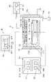
- FIG. 1 is a longitudinal sectional view showing a configuration example of a plasma processing system according to this embodiment;
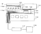
- FIG. 1 is a longitudinal sectional view showing a configuration example of a substrate support according to this embodiment;
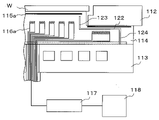
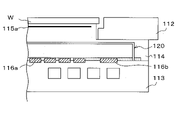
- FIG. 10 is a vertical cross-sectional view showing a configuration example of a substrate support according to another embodiment;
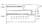
- FIG. 10 is a vertical cross-sectional view showing a configuration example of a substrate support according to another embodiment;
- FIG. 10 is an explanatory diagram showing the flow of high-frequency power in a conventional substrate support;
- FIG. 4 is an explanatory diagram showing the flow of high-frequency power in the substrate support according to the embodiment;
- FIG. 10 is a vertical cross-sectional view showing a configuration example of a substrate support according to another embodiment;
- FIG. 10 is a vertical cross-sectional view showing a configuration example of a substrate support according to another embodiment
- FIG. 10 is a vertical cross-sectional view showing a configuration example of a substrate support according to another embodiment
- FIG. 10 is a vertical cross-sectional view showing a configuration example of a substrate support according to another embodiment
- FIG. 10 is a vertical cross-sectional view showing a configuration example of a substrate support according to another embodiment
- FIG. 10 is a vertical cross-sectional view showing a configuration example of a substrate support according to another embodiment
- FIG. 10 is a vertical cross-sectional view showing a configuration example of a substrate support according to another embodiment
- FIG. 2 is a vertical cross-sectional view showing a configuration example of an upper electrode mechanism according to one embodiment
- a semiconductor substrate supported by a substrate support (hereinafter simply referred to as "substrate") is etched by exciting a processing gas supplied in a chamber to generate plasma.
- Various plasma treatments such as treatment, film formation, and diffusion are performed.
- a substrate support for supporting a substrate is provided with, for example, an electrostatic chuck that attracts and holds the substrate on a mounting surface by Coulomb force or the like, and an electrode section to which high-frequency power is applied during plasma processing.
- a plurality of heating elements are provided inside the electrostatic chuck, and the mounting surface temperature is controlled for each of a plurality of temperature control regions defined by these heating elements. is adjusted by A plurality of heating elements arranged inside the electrostatic chuck are connected to a heating element power supply for supplying power to the heating elements via corresponding power supply cables.
- high frequency noise part of the high frequency applied to the electrode part from the RF (Radio Frequency) power supply during plasma generation is common mode noise (hereinafter simply referred to as "high frequency noise ”) may cause abnormal discharge or backflow of high-frequency power.
- high frequency noise especially when high-frequency noise that has entered reaches the power source for the heating element, there is a risk of inducing damage or malfunction of the power source for the heating element. Therefore, in the plasma processing apparatus, as disclosed in Patent Document 1, an RF cut filter (filter unit) for attenuating or blocking high-frequency noise may be arranged on the power supply cable (line). It is done.
- the RF cut filter attempts to attenuate the high-frequency noise that has entered the power supply cable, but the high-frequency noise cannot be completely blocked. There is a risk that the heat will reach the power source for the heating element. If part of the high-frequency noise reaches the power source for the heating element in this way, it may cause damage or malfunction of the power source for the heating element, as described above.
- the RF cut filter placed on the power supply cable acts as a resistance when high frequency noise passes through, this may cause loss of high frequency power and reduce power efficiency. Furthermore, if there is a variation in the resistance value of the RF cut filter arranged on the power supply cable, there is a possibility that the variation in the resistance value will appear as an instrumental difference in the plasma processing apparatus.
- FIG. 1 is a longitudinal sectional view showing the outline of the configuration of the plasma processing system according to this embodiment.
- the plasma processing system includes a capacitively coupled plasma processing apparatus 1 and a controller 2.
- the plasma processing apparatus 1 includes a plasma processing chamber 10 , a gas supply section 20 , a power supply 30 and an exhaust system 40 .
- the plasma processing apparatus 1 also includes a substrate support 11 and a gas inlet.
- a substrate support 11 is positioned within the plasma processing chamber 10 .
- the gas introduction is configured to introduce at least one process gas into the plasma processing chamber 10 .
- the gas introduction section includes a showerhead 13 .
- a showerhead 13 is positioned above the substrate support 11 . In one embodiment, showerhead 13 forms at least a portion of the ceiling of plasma processing chamber 10 .
- the plasma processing chamber 10 has at least one gas supply port for supplying at least one processing gas to the plasma processing space 10s and at least one gas exhaust port for exhausting gas from the plasma processing space 10s.
- Plasma processing chamber 10 is grounded.
- showerhead 13 and substrate support 11 are electrically isolated from plasma processing chamber 10 .
- the substrate support 11 includes a body member 111 and a ring assembly 112 as an electrode mechanism.
- the top surface of body member 111 has a central region 111a (substrate support surface) for supporting a substrate (wafer) W and an annular region 111b (ring support surface) for supporting ring assembly 112 .
- the annular region 111b surrounds the central region 111a in plan view.
- Ring assembly 112 includes one or more annular members, at least one of which is an edge ring.
- the body member 111 includes a base 113 and an electrostatic chuck 114 as electrode units.
- the base 113 and the electrostatic chuck 114 are laminated and joined with an adhesive member G interposed therebetween.
- the electrostatic chuck 114 and the adhesive member G that constitute the main body member 111 correspond to the “dielectric portion” according to the technique of the present disclosure.
- the base 113 is made of a conductive member such as Al alloy.
- the conductive member of base 113 functions as a lower electrode.
- a channel C is formed inside the base 113 .
- a heat transfer medium (temperature control fluid) from a chiller unit (not shown) is circulated and supplied to the flow path C. As shown in FIG. By circulating the heat transfer medium in the flow path C, the ring assembly 112, the electrostatic chuck 114, which will be described later, and the substrate W are adjusted to desired temperatures.
- a coolant such as cooling water can be used as the heat transfer medium.
- the electrostatic chuck 114 is layered and joined to the upper surface of the base 113 .
- the upper surface of the electrostatic chuck 114 has the aforementioned central region 111a and annular region 111b.
- An adsorption electrode 115 , a heater electrode 116 and a shield member 120 are provided inside the electrostatic chuck 114 .
- the electrostatic chuck 114 is configured by sandwiching an adsorption electrode 115, a heater electrode 116, and a shield member 120 between a pair of dielectric films made of a non-magnetic dielectric such as ceramics.
- the attraction electrode 115 has a first attraction electrode 115a for attracting and holding the substrate W to the central region 111a, and a second attraction electrode 115b for attracting and holding the ring assembly 112 to the annular region 111b.
- the attracting electrode 115 is connected to an attracting power supply (not shown). By applying a voltage from the attracting power supply to the attracting electrode 115, an electrostatic force such as a Coulomb force is generated. W is held by adsorption.
- the power source 30 shown in FIG. 1 and described later may be used as the power source for adsorption, or a power source for adsorption (not shown) independent of the power source 30 may be connected.
- the heater electrode 116 as an electric circuit has one or more first heater electrodes 116 a for heating the substrate W and one or more second heater electrodes 116 b for heating the ring assembly 112 .
- a heating power source 118 is connected to the heater electrode 116 via an RF cut filter 117 .
- the heater electrode 116 heats at least one of the ring assembly 112 , the electrostatic chuck 114 and the substrate W by applying power from the heating power supply 118 .
- the RF cut filter 117 cuts off the noise when high-frequency power applied to the conductive member of the base 113 from the RF power source 31 (to be described later) enters the heater electrode 116 as a noise component when plasma is generated in the plasma processing space 10s. It prevents the components from reaching the heating power source 118 .
- the heating power source 118 is configured such that the power supply to each of the plurality of heater electrodes 116 can be individually controlled by, for example, the control unit 2 described later.
- the electrostatic chuck 114 has a central region 111a (substrate W) and an annular region 111b (ring assembly 112) for each of a plurality of temperature control regions defined by each or a combination of the plurality of heater electrodes 116 in plan view. temperature can be controlled.
- the heating power source 118 the power source 30 shown in FIG. 1 and described later may be used, or a heating power source 118 independent of the power source 30 may be connected.
- the shield member 120 is made of, for example, a conductive metal material having a sufficiently low resistance to the high frequency power applied to the conductive member of the base 113. made of a conductive metallic material (eg, tungsten, titanium, etc.) that attenuates or blocks the
- the shield member 120 is provided inside the electrostatic chuck 114 so as to surround at least the heater electrode 116 .
- the shield member 120 includes a substantially disk-shaped first top plate member 121 arranged to cover the first heater electrode 116a in a plan view, and a second heater electrode 116b. , and a substantially cylindrical first side wall member 123 arranged to surround the first heater electrode 116a in a side view. and a substantially cylindrical second side wall member 124 arranged to surround the second heater electrode 116b in a side view.
- the shield member 120 is provided inside the electrostatic chuck 114 on the opposite side of the base 113 with respect to the heater electrode 116 in the stacking direction of the base 113 and the electrostatic chuck 114 . It has a plate member. The shield member 120 also has a side wall member provided radially outside the heater electrode 116 inside the electrostatic chuck 114 .
- the first top plate member 121 is arranged along the surface direction of the electrostatic chuck 114 between the first adsorption electrode 115a and the first heater electrode 116a.
- the second top plate member 122 is arranged along the surface direction between the second adsorption electrode 115b and the second heater electrode 116b.
- the first side wall member 123 is arranged in the stacking direction of the base 113 and the electrostatic chuck 114 , that is, the electrostatic chuck 114 so as to electrically connect the first top plate member 121 and the second top plate member 122 .
- the second side wall member 124 is arranged along the stacking direction (thickness direction) so as to electrically connect the second top plate member 122 and the base 113 . That is, in one embodiment, the shield member 120 is arranged inside the electrostatic chuck 114 so as to have substantially the same potential as the base 113 .
- the heater electrode 116 arranged inside the electrostatic chuck 114 has the same potential space S ( 2) so as to be substantially housed therein.
- the first top plate member 121 and the second top plate member 122 arranged along the surface direction of the electrostatic chuck 114 are attracted in comparison with the heater electrode 116 in the thickness direction of the electrostatic chuck 114 .
- the electrode 115 (more preferably, the surface of the electrostatic chuck 114) be arranged at a position close to it.
- the distance between the heater electrode 116 and the top plate member is made larger than the distance between the adsorption electrode 115 (more preferably, the surface of the electrostatic chuck 114) and the top plate member.
- the position of the top plate member is determined.
- the substrate support 11 has a heat transfer gas supply unit configured to supply a heat transfer gas (backside gas) between the back surface of the substrate W and the top surface of the electrostatic chuck 114.
- a heat transfer gas backside gas
- the showerhead 13 is configured to introduce at least one processing gas from the gas supply 20 into the plasma processing space 10s.
- the showerhead 13 has at least one gas supply port 13a, at least one gas diffusion chamber 13b, and multiple gas introduction ports 13c.
- the processing gas supplied from the gas supply unit 20 to the gas supply port 13a passes through the gas diffusion chamber 13b and is introduced into the plasma processing space 10s through a plurality of gas introduction ports 13c.
- showerhead 13 also includes a conductive member.
- a conductive member of the showerhead 13 functions as an upper electrode.
- the gas introduction part may include one or more side gas injectors (SGI: Side Gas Injector) attached to one or more openings formed in the side wall 10a.
- SGI Side Gas Injector
- the gas supply unit 20 may include at least one gas source 21 and at least one flow controller 22 .
- gas supply 20 is configured to supply at least one process gas from respective gas sources 21 through respective flow controllers 22 to showerhead 13 .
- Each flow controller 22 may include, for example, a mass flow controller or a pressure controlled flow controller.
- gas supply 20 may include one or more flow modulation devices that modulate or pulse the flow of at least one process gas.
- Power supply 30 includes an RF power supply 31 coupled to plasma processing chamber 10 via at least one impedance matching circuit.
- the RF power supply 31 applies at least one RF signal (RF power), such as a source RF signal and a bias RF signal, to a conductive member of the substrate support 11 (lower electrode) or a conductive member of the showerhead 13 (upper electrode). to at least one of Thereby, plasma is formed from at least one processing gas supplied to the plasma processing space 10s.
- RF power source 31 may function as at least part of a plasma generator configured to generate a plasma from one or more process gases in plasma processing chamber 10 . Further, by supplying a bias RF signal to the lower electrode, a bias potential is generated in the substrate W, and ion components in the formed plasma can be drawn into the substrate W.
- the RF power supply 31 includes a first RF generator 31a and a second RF generator 31b.
- the first RF generator 31a is coupled to at least one of the lower electrode and the upper electrode via at least one impedance matching circuit and configured to generate a source RF signal (source RF power) for plasma generation.
- the source RF signal has a frequency within the range of 13 MHz to 150 MHz.
- the first RF generator 31a may be configured to generate multiple source RF signals having different frequencies.
- One or more source RF signals generated are provided to at least one of the bottom electrode or the top electrode.
- a second RF generator 31b is coupled to the lower electrode via at least one impedance matching circuit and configured to generate a bias RF signal (bias RF power).
- the bias RF signal has a lower frequency than the source RF signal.
- the bias RF signal has a frequency within the range of 400 kHz to 13.56 MHz.
- the second RF generator 31b may be configured to generate multiple bias RF signals having different frequencies.
- One or more bias RF signals generated are provided to the bottom electrode. Also, in various embodiments, at least one of the source RF signal and the bias RF signal may be pulsed.
- Power supply 30 may also include a DC power supply 32 coupled to plasma processing chamber 10 .
- the DC power supply 32 includes a first DC generator 32a and a second DC generator 32b.
- the first DC generator 32a is connected to the bottom electrode and configured to generate a first DC signal.
- the generated first bias DC signal is applied to the bottom electrode.
- the first DC signal may be applied to other electrodes, such as attracting electrode 115 within electrostatic chuck 114 .
- the second DC generator 32b is connected to the upper electrode and configured to generate the second DC signal.
- the generated second DC signal is applied to the upper electrode.
- at least one of the first and second DC signals may be pulsed. Note that the first and second DC generators 32a and 32b may be provided in addition to the RF power supply 31, and the first DC generator 32a may be provided instead of the second RF generator 31b. good.
- the exhaust system 40 may be connected to a gas exhaust port 10e provided at the bottom of the plasma processing chamber 10, for example.
- Exhaust system 40 may include a pressure regulating valve and a vacuum pump. The internal pressure of the plasma processing space 10s is adjusted by the pressure regulating valve.
- Vacuum pumps may include turbomolecular pumps, dry pumps, or combinations thereof.
- the controller 2 processes computer-executable instructions that cause the plasma processing apparatus 1 to perform the various steps described in this disclosure. Controller 2 may be configured to control elements of plasma processing apparatus 1 to perform the various processes described herein. In one embodiment, part or all of the controller 2 may be included in the plasma processing apparatus 1 .
- the control unit 2 may include, for example, a computer 2a.
- the computer 2a may include, for example, a processing unit (CPU: Central Processing Unit) 2a1, a storage unit 2a2, and a communication interface 2a3. Processing unit 2a1 can be configured to perform various control operations based on programs stored in storage unit 2a2.
- the storage unit 2a2 may include RAM (Random Access Memory), ROM (Read Only Memory), HDD (Hard Disk Drive), SSD (Solid State Drive), or a combination thereof.
- the communication interface 2a3 may communicate with the plasma processing apparatus 1 via a communication line such as a LAN (Local Area Network).
- the plasma processing system may be an inductively coupled plasma (ICP), an electron-cyclotron-resonance plasma (ECR plasma), a helicon wave excited plasma (HWP), or a surface wave plasma (SWP). It may have a processing apparatus including a plasma generation unit such as Plasma. Also, processing apparatus including various types of plasma generators may be used, including alternating current (AC) plasma generators and direct current (DC) plasma generators.
- ICP inductively coupled plasma
- ECR plasma electron-cyclotron-resonance plasma
- HWP helicon wave excited plasma
- SWP surface wave plasma
- processing apparatus including various types of plasma generators may be used, including alternating current (AC) plasma generators and direct current (DC) plasma generators.
- the heater electrode 116 includes a first heater electrode 116a for heating the substrate W and a second heater electrode 116b for heating the ring assembly 112.
- the second heater electrode 116b for heating the ring assembly 112 can be appropriately omitted as shown in FIG.
- the side wall member 123 may be configured to electrically connect the first top plate member 121 and the base 113 .
- the shield member 120 made of a conductive metal material having a sufficiently low resistance to high-frequency power is arranged inside the electrostatic chuck 114 . .
- the high-frequency power applied to the conductive member of the base 113 during plasma processing propagates on the surface of the base 113, which is a conductive member, and is supplied to the plasma processing space.
- the conventional substrate support 11' in which the shield member 120 is not arranged as shown in FIG.
- Part of the high-frequency power propagating on the surface of the base 113 may enter. More specifically, due to the potential difference between the base 113 and the heater electrode 116, part of the high-frequency power propagating on the surface of the base 113 enters the heater electrode 116 as a noise component, further increasing the potential difference. Discharge may occur at The noise components that enter the heater electrode 116 and the generated discharge may cause damage to the heater electrode 116 and the heating power supply 118, and may cause a decrease in power efficiency.
- the shield member 120 is provided inside the electrostatic chuck 114 so as to have substantially the same potential as the base 113 .
- the high-frequency power propagates through the surface of the shield member 120 instead of the surface of the base 113, as shown in FIG. Therefore, high-frequency power is suppressed from propagating on the surface of base 113 and reaching the vicinity of heater electrode 116 , thereby appropriately suppressing entry of high-frequency power into heater electrode 116 .
- the heater electrode 116 which may be exposed to high-frequency power, is placed in the same-potential space S defined by the base 113 and the shield member 120, which are arranged so as to have substantially the same potential. housed inside the As a result, generation of a potential difference between the heater electrode 116 and the base 113 is suppressed inside the same-potential space S, so that high-frequency power is more appropriately suppressed from entering the heater electrode 116 .
- the high-frequency power applied to the conductive member of the base 113 in this way propagates through the surface of the shield member 120 and reaches the vicinity of the surface of the electrostatic chuck 114, that is, the vicinity of the plasma processing space 10s. , thereby improving plasma generation efficiency during plasma processing.
- the first top plate member 121 and the second top plate member 122 are arranged with respect to the adsorption electrode 115 (the surface of the electrostatic chuck 114) as compared with the heater electrode 116. Plasma generation efficiency can be improved more appropriately by arranging them in close positions.
- the heater electrode 116 is accommodated in the same potential space S defined by the base 113 and the shield member 120 which are arranged to have substantially the same potential.
- the case of arrangement has been described as an example.
- the configuration of the substrate support 11 is not limited to this, and any configuration can be employed as long as it can at least attenuate or prevent the high-frequency power from entering the heater electrode 116 .
- the first top plate member 121 may be configured in a substantially annular shape so as to cover at least a portion of the first heater electrode 116a in plan view.
- the heater electrode 116 does not necessarily have to be arranged so as to be accommodated inside the same-potential space S.
- the high-frequency power is applied to the second side wall member 124, the second top plate member 122, and the first side wall member 123.
- the first top plate member 121 in a substantially annular shape in this way, the heat generated by the first heater electrode 116a can be transferred directly to the substrate W without going through the first top plate member 121. Since heat can be transferred, the heating efficiency of the substrate W by the first heater electrode 116a can be improved.
- the shield member 120 allows the high-frequency power to reach the vicinity of the surface of the electrostatic chuck 114 in this way, the first top plate member 121 may be omitted as shown in FIG. Even in such a case, it is possible to at least attenuate the intrusion of the high-frequency power to the first heater electrode 116a, and to improve the heating efficiency of the substrate W by the first heater electrode 116a.
- both the first top plate member 121 and the second top plate member 122 of the shield member 120 may be omitted.
- the shield member 120 may be composed only of the side wall members (the first side wall member 123 or the second side wall member 124). Specifically, when the heater electrode 116 includes the first heater electrode 116a and the second heater electrode 116b as shown in FIG. Moreover, when the heater electrode 116 includes only the first heater electrode 116a as shown in FIG.
- the upper end of the shield member 120 (the first side wall member 123 or the second side wall member 124 ) should be positioned at least above the heater electrode 116 , more preferably near the surface of the electrostatic chuck 114 . By doing so, it is possible to at least attenuate the penetration of the high-frequency power to the first heater electrode 116a.
- the high-frequency power applied to the conductive member of the base 113 propagates through the surfaces of the base 113 and the shield member 120 and near the surface of the electrostatic chuck 114, that is, for example, the first The top plate member 121 is reached. However, at this time, if at least part of the first top plate member 121 is omitted as shown in FIGS. There is a possibility that the uniformity of plasma processing results for W may be biased.
- the shield member 120 (specifically, the first top plate member 121 and the A second top plate member 122) is preferably arranged.
- the electrostatic chuck 114 that holds the substrate W is generally configured to have a sufficiently large size in the radial direction compared to the size in the thickness direction. Specifically, for example, while the size of the electrostatic chuck 114 in the radial direction is about 300 mm or more to match the size of the substrate W, the size of the electrostatic chuck 114 in the thickness direction is about 10 mm or less. It is. For this reason, in the electrostatic chuck 114 according to the present embodiment, when the shield member 120 is arranged inside, impedance design is performed by changing the installation position, thickness, etc.
- the shield member 120 does not necessarily have to be arranged to have substantially the same potential as the base 113 .
- the first top plate member 121 As the shield member 120 in this way, high-frequency power can be propagated over the entire surface of the first top plate member 121 (electrostatic chuck 114) in plan view. As a result, the uniformity of plasma processing results for the substrate W can be improved.
- holes are formed in the first top plate member 121 and the second top plate member 122 of the shield member 120 in order to appropriately suppress penetration of high-frequency power into the heater electrode 116. It was formed by a plate-shaped member that was not Similarly, the first side wall member 123 and the second side wall member 124 are each formed of a plate-like member without a hole, so that the base 113 and the shield member 120 are arranged around the heater electrode 116. Line contact was made to surround with.
- the configuration of the shield member 120 is not limited to this as long as it can at least dampen the entry of high-frequency power into the heater electrode 116 .
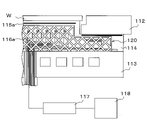
- the side wall members of the shield member 120 may be formed in a lattice shape (mesh shape) as shown in FIG.
- one or more holes may be formed in the top plate member and side wall members of the shield member 120 .
- the high-frequency power propagating on the surface of the base 113 can be propagated along the surface of the shield member 120, that is, the amount of high-frequency power propagating in the vicinity of the heater electrode 116 can be attenuated. As a result, penetration of high-frequency power into the heater electrode 116 can be suppressed.
- the first top plate member 121 is formed in a grid pattern in this way, high-frequency power can be propagated over the entire surface of the first top plate member 121 (electrostatic chuck 114) in plan view. As a result, the uniformity of plasma processing results for the substrate W can be improved.
- the sidewall members of the shield member 120 in a vertical grid pattern, at least the amount of high-frequency power propagating in the vicinity of the heater electrode 116 can be attenuated. , the intrusion of high-frequency power into the heater electrode 116 can be suppressed.
- the top plate member of the shield member 120 is formed in a grid shape or a vertical lattice shape. It may be configured in a vertical lattice shape. Even when the top plate member is calibrated in a grid pattern or a vertical grid pattern in this manner, high-frequency power can be propagated over the entire surface of the electrostatic chuck 114 in plan view, and as a result, the plasma processing result for the substrate W can be obtained. uniformity can be improved.
- the contact point positions are located around the heater electrode 116. If they are not uniformly arranged, the plasma processing result may be biased, or the shield member 120 and the base 113 may not be appropriately configured to have approximately the same potential. Therefore, when the shield member 120 and the base 113 are brought into point contact with each other in this way, it is desirable to arrange such contact point positions evenly over the entire circumference of the electrostatic chuck 114 . Specifically, for example, when six contact points are designed, it is desirable that the contact points are arranged at intervals of 60 degrees in the circumferential direction. When the shield member 120 and the base 113 are brought into point contact in this way, the number of such contact points should be increased as much as possible in order to appropriately configure the shield member 120 and the base 113 to have the same potential. is desirable.
- the shield member 120 separates the first heater electrode 116a and the second heater electrode 116b. are housed integrally in the same potential space S, the first heater electrode 116a and the second heater electrode 116b may be housed in the same potential space S independently of each other. In other words, by arranging a plurality of shield members 120 inside the electrostatic chuck 114, a plurality of spaces S having the same potential are formed. heater electrode 116b may be arranged.
- the heater electrode 116 may be arranged inside the electrostatic chuck 114 as a dielectric portion or inside the adhesive member G as long as it is inside the electrostatic chuck 114 . and the adhesive member G. In one embodiment, the heater electrode 116 may be in contact with the base 113 on one side as shown in FIG. Alternatively, a portion may be embedded in the base 113 as shown in FIG.
- the RF cut filter 117 for attenuating or blocking high-frequency power is provided on the power supply cable connecting the heater electrode 116 and the heating power supply 118. is provided.
- the shield member 120 cannot completely prevent high-frequency power from entering the heater electrode 116, it is possible to appropriately suppress noise components from reaching the heating power source 118.
- the effect of the shield member 120 at least attenuates the amount of high-frequency power that enters the heater electrode 116, so that the heating power supply 118 can be more easily protected by the RF cut filter 117. .
- high-frequency power entering the heater electrode 116 can be attenuated or blocked only by the effect of the shield member 120 . Therefore, in the substrate support 11 according to this embodiment, the RF cut filter 117 arranged on the power supply cable can be appropriately reduced in size or omitted.
- a plurality of RF cut filters 117 are usually provided in the space below the substrate support 11 (electrostatic chuck 114) corresponding to each of the plurality of heater electrodes 116 or each of the plurality of temperature control regions defined by the combination. There is a need. That is, it is necessary to arrange a plurality of RF cut filters 117 and power supply cables for connecting them in the space below the substrate support 11, which may occupy the space below the substrate support 11. rice field.
- the RF cut filter 117 can be miniaturized or omitted as described above. Therefore, the power supply cable and the RF cut filter 117 arranged in the lower space of the substrate support 11 (electrostatic chuck 114) can be reduced, and the space efficiency of the lower space can be improved. This cost can be reduced.
- the RF cut filter 117 acts as a resistance, thereby In some cases, power efficiency decreased. Moreover, at this time, especially when the resistance value of the RF cut filter 117 varies, the variation in the resistance value may appear as an instrumental difference of the plasma processing apparatus 1 . In this respect, according to the present embodiment, since the installation of the RF cut filter 117 can be omitted in this way, the power loss due to the RF cut filter 117 can be suppressed, and the power efficiency can be improved. You can improve the difference problem.
- the shield member 120 for suppressing or blocking the entry of high-frequency power into the electric circuit is placed inside the electrostatic chuck 114, more broadly inside the substrate support 11 constituting the lower electrode mechanism.
- the case of arranging inside is explained as an example.
- the installation position of the shield member according to the technology of the present disclosure is not limited to this, and can be arranged on any member that internally includes an electric circuit that should suppress the intrusion of high-frequency power.
- the shield member may be arranged inside the upper electrode mechanism.
- FIG. 14 is a cross-sectional view showing the outline of the configuration of the upper electrode mechanism 130 according to one embodiment.
- the upper electrode mechanism 130 includes a metal plate 131 as an electrode portion and a showerhead 132 .
- the metal plate 131 and the showerhead 132 are laminated with an adhesive member G interposed therebetween.
- the shower head 132 and the adhesive member G that constitute the upper electrode mechanism 130 correspond to the “dielectric portion” according to the technique of the present disclosure.
- the metal plate 131 is made of a conductive member such as Al alloy.
- the conductive member of metal plate 131 functions as an upper electrode.
- a gas supply port 13a and a gas diffusion chamber 13b are formed inside the metal plate 131.
- the metal plate 131 also has at least one channel C inside for controlling the temperature of the shower head 132 whose temperature fluctuates due to the heat input of the plasma.
- a heat transfer medium (temperature control fluid) from a chiller unit (not shown) is circulated and supplied to the flow path C. As shown in FIG.
- a plurality of gas introduction ports 13c are formed through the shower head 132 in the thickness direction (vertical direction).
- the gas introduction port 13c is connected to the gas supply unit 20 via a gas diffusion chamber 13b formed inside the metal plate 131 and a gas supply port 13a, and supplies at least one processing gas from the gas supply unit 20 to the plasma. configured to introduce into the processing space 10s.
- the showerhead 132 also has at least one heater electrode 140 therein for controlling the temperature of the showerhead 132 whose temperature fluctuates due to the heat input of the plasma. Note that in the present embodiment, the heater electrode 140 corresponds to the "electric circuit" according to the technique of the present disclosure.
- high-frequency power applied to the conductive member (upper electrode) of the metal plate 131 enters the heater electrode 140 .
- a shield member 150 is arranged to attenuate or block the The shield member 150 is made of, for example, a conductive metal material (eg, tungsten, titanium, etc.) having a sufficiently low resistance value with respect to high frequency power applied to the upper electrode.
- the shield member 150 is arranged inside the shower head 132 so as to surround at least the heater electrode 140 and have the same potential as the metal plate 131 .
- the upper electrode mechanism 130 has the same potential defined by the metal plate 131 and the shield member 120, which are arranged so that the heater electrode 140, which is likely to be invaded by high-frequency power, has substantially the same potential. It is housed inside the space S.
- the shield member 150 inside the shower head 132 in this way, the high-frequency power applied to the upper electrode is transferred to the metal plate 131 and the shield member 150 It propagates on the surface and reaches the vicinity of the surface of the shower head 132, that is, the vicinity of the plasma processing space 10s. As a result, it is possible to appropriately prevent the high-frequency power from entering the heater electrode 140 .
- the configuration of the shield member 150 arranged inside the shower head 132 is not limited to the illustrated example. That is, like the shield member 120 arranged inside the electrostatic chuck 114, either the top plate member or the side wall member constituting the shield member 150 may be omitted, or the top plate member or the side wall member may be omitted. may be configured in a lattice shape or vertical lattice shape.
- the arrangement of the heater electrode 140 as an electric circuit is not limited to the example shown in the drawing, and may be arranged so that at least a portion of the heater electrode 140 is in contact with the dielectric portion.
- the heater electrode 140 may be arranged inside the adhesive member G as long as it is inside the shower head 132 as the dielectric portion or the adhesive member G, or may be attached to the shower head 132 . It may be arranged so as to straddle the member G.
- the heater electrode 140 may be in contact with the metal plate 131 on one side, or may be partially in contact with the metal plate 131 as long as the heater electrode 140 is in contact with the shower head 132 as the dielectric portion or the adhesive member G. may be embedded in
- the shield member according to the technique of the present disclosure is not limited to the inside of the electrostatic chuck 114 of the lower electrode mechanism, and any member that has an electric circuit inside to prevent high-frequency power from entering. can be placed inside the
- the shield member can be arranged to protect any electric circuit that may malfunction due to intrusion of high-frequency power, such as thermocouples, piezo elements, drive mechanisms of other parts, and the like.
Landscapes
- Engineering & Computer Science (AREA)
- Physics & Mathematics (AREA)
- Plasma & Fusion (AREA)
- Chemical & Material Sciences (AREA)
- Analytical Chemistry (AREA)
- Power Engineering (AREA)
- Electromagnetism (AREA)
- Spectroscopy & Molecular Physics (AREA)
- Drying Of Semiconductors (AREA)
- Plasma Technology (AREA)
- Treatment Of Fiber Materials (AREA)
- Physical Or Chemical Processes And Apparatus (AREA)
Priority Applications (4)
| Application Number | Priority Date | Filing Date | Title |
|---|---|---|---|
| JP2023513012A JP7682260B2 (ja) | 2021-04-06 | 2022-04-04 | プラズマ処理装置及び電極機構 |
| KR1020237030767A KR20230164658A (ko) | 2021-04-06 | 2022-04-04 | 플라즈마 처리 장치 및 전극 기구 |
| US18/239,006 US20230402263A1 (en) | 2021-04-06 | 2023-08-28 | Plasma treatment device and electrode mechanism |
| JP2025080664A JP2025114799A (ja) | 2021-04-06 | 2025-05-13 | プラズマ処理装置及び基板支持体 |
Applications Claiming Priority (2)
| Application Number | Priority Date | Filing Date | Title |
|---|---|---|---|
| JP2021064704 | 2021-04-06 | ||
| JP2021-064704 | 2021-04-06 |
Related Child Applications (1)
| Application Number | Title | Priority Date | Filing Date |
|---|---|---|---|
| US18/239,006 Continuation US20230402263A1 (en) | 2021-04-06 | 2023-08-28 | Plasma treatment device and electrode mechanism |
Publications (1)
| Publication Number | Publication Date |
|---|---|
| WO2022215680A1 true WO2022215680A1 (ja) | 2022-10-13 |
Family
ID=83546097
Family Applications (1)
| Application Number | Title | Priority Date | Filing Date |
|---|---|---|---|
| PCT/JP2022/017038 Ceased WO2022215680A1 (ja) | 2021-04-06 | 2022-04-04 | プラズマ処理装置及び電極機構 |
Country Status (5)
| Country | Link |
|---|---|
| US (1) | US20230402263A1 (https=) |
| JP (2) | JP7682260B2 (https=) |
| KR (1) | KR20230164658A (https=) |
| TW (1) | TW202303648A (https=) |
| WO (1) | WO2022215680A1 (https=) |
Cited By (1)
| Publication number | Priority date | Publication date | Assignee | Title |
|---|---|---|---|---|
| WO2026042624A1 (ja) * | 2024-08-22 | 2026-02-26 | 東京エレクトロン株式会社 | プラズマ処理装置 |
Citations (5)
| Publication number | Priority date | Publication date | Assignee | Title |
|---|---|---|---|---|
| JP2014229734A (ja) * | 2013-05-22 | 2014-12-08 | 東京エレクトロン株式会社 | エッチング方法及びエッチング装置 |
| JP2017028111A (ja) * | 2015-07-23 | 2017-02-02 | 株式会社日立ハイテクノロジーズ | プラズマ処理装置 |
| JP2019140155A (ja) * | 2018-02-06 | 2019-08-22 | 株式会社日立ハイテクノロジーズ | プラズマ処理装置 |
| WO2020055565A1 (en) * | 2018-09-14 | 2020-03-19 | Applied Materials, Inc. | Semiconductor substrate supports with embedded rf shield |
| JP2020068247A (ja) * | 2018-10-23 | 2020-04-30 | 東京エレクトロン株式会社 | シャワーヘッドおよび基板処理装置 |
Family Cites Families (1)
| Publication number | Priority date | Publication date | Assignee | Title |
|---|---|---|---|---|
| JP6218650B2 (ja) | 2014-03-11 | 2017-10-25 | 東京エレクトロン株式会社 | プラズマ処理装置 |
-
2022
- 2022-04-04 JP JP2023513012A patent/JP7682260B2/ja active Active
- 2022-04-04 WO PCT/JP2022/017038 patent/WO2022215680A1/ja not_active Ceased
- 2022-04-04 KR KR1020237030767A patent/KR20230164658A/ko active Pending
- 2022-04-06 TW TW111112999A patent/TW202303648A/zh unknown
-
2023
- 2023-08-28 US US18/239,006 patent/US20230402263A1/en active Pending
-
2025
- 2025-05-13 JP JP2025080664A patent/JP2025114799A/ja active Pending
Patent Citations (5)
| Publication number | Priority date | Publication date | Assignee | Title |
|---|---|---|---|---|
| JP2014229734A (ja) * | 2013-05-22 | 2014-12-08 | 東京エレクトロン株式会社 | エッチング方法及びエッチング装置 |
| JP2017028111A (ja) * | 2015-07-23 | 2017-02-02 | 株式会社日立ハイテクノロジーズ | プラズマ処理装置 |
| JP2019140155A (ja) * | 2018-02-06 | 2019-08-22 | 株式会社日立ハイテクノロジーズ | プラズマ処理装置 |
| WO2020055565A1 (en) * | 2018-09-14 | 2020-03-19 | Applied Materials, Inc. | Semiconductor substrate supports with embedded rf shield |
| JP2020068247A (ja) * | 2018-10-23 | 2020-04-30 | 東京エレクトロン株式会社 | シャワーヘッドおよび基板処理装置 |
Cited By (1)
| Publication number | Priority date | Publication date | Assignee | Title |
|---|---|---|---|---|
| WO2026042624A1 (ja) * | 2024-08-22 | 2026-02-26 | 東京エレクトロン株式会社 | プラズマ処理装置 |
Also Published As
| Publication number | Publication date |
|---|---|
| TW202303648A (zh) | 2023-01-16 |
| US20230402263A1 (en) | 2023-12-14 |
| JP7682260B2 (ja) | 2025-05-23 |
| JP2025114799A (ja) | 2025-08-05 |
| JPWO2022215680A1 (https=) | 2022-10-13 |
| KR20230164658A (ko) | 2023-12-04 |
Similar Documents
| Publication | Publication Date | Title |
|---|---|---|
| KR102594442B1 (ko) | 플라즈마 처리 장치 | |
| CN108281342B (zh) | 等离子体处理装置 | |
| CN109509694B (zh) | 等离子体处理装置和等离子体处理方法 | |
| US20230090650A1 (en) | Plasma processing apparatus | |
| US20220130645A1 (en) | Plasma processing apparatus | |
| JP2023044634A (ja) | プラズマ処理装置 | |
| TW202329196A (zh) | 電漿處理裝置 | |
| JP7246450B2 (ja) | 基板処理装置及び基板処理方法 | |
| JP2025114799A (ja) | プラズマ処理装置及び基板支持体 | |
| TW202326928A (zh) | 基板支撐器、電漿處理裝置及電漿處理方法 | |
| JP7690575B2 (ja) | 下部電極機構及び基板処理装置 | |
| KR102770730B1 (ko) | 기판 처리 장치 및 기판 처리 방법 | |
| TWI917607B (zh) | 電漿處理裝置用之電極及電漿處理裝置 | |
| US12562344B2 (en) | Plasma processing apparatus | |
| JP7781702B2 (ja) | 基板支持アセンブリ、基板支持体、基板処理装置、及び基板処理方法 | |
| JP7150946B2 (ja) | 基板処理装置及び基板処理方法 | |
| JP2023097106A (ja) | プラズマ処理装置 | |
| JP2024018988A (ja) | 基板支持器及びプラズマ処理装置 | |
| WO2024142924A1 (ja) | プラズマ処理装置及び誘電体窓 | |
| JP2024115405A (ja) | プラズマ処理装置 | |
| WO2024150693A1 (ja) | 支持体、基板支持器及びプラズマ処理装置 | |
| TW202341344A (zh) | 基板支持器及電漿處理裝置 | |
| TW202509993A (zh) | 電漿處理裝置、基板支持部及邊緣環之消耗修正方法 | |
| JP2024014108A (ja) | プラズマ処理装置、載置台及びプラズマ処理方法 | |
| JP2022166511A (ja) | プラズマ処理装置用の電極及びプラズマ処理装置 |
Legal Events
| Date | Code | Title | Description |
|---|---|---|---|
| 121 | Ep: the epo has been informed by wipo that ep was designated in this application |
Ref document number: 22784662 Country of ref document: EP Kind code of ref document: A1 |
|
| WWE | Wipo information: entry into national phase |
Ref document number: 2023513012 Country of ref document: JP |
|
| NENP | Non-entry into the national phase |
Ref country code: DE |
|
| 122 | Ep: pct application non-entry in european phase |
Ref document number: 22784662 Country of ref document: EP Kind code of ref document: A1 |