WO2022202038A1 - 電子部品およびその製造方法 - Google Patents
電子部品およびその製造方法 Download PDFInfo
- Publication number
- WO2022202038A1 WO2022202038A1 PCT/JP2022/007002 JP2022007002W WO2022202038A1 WO 2022202038 A1 WO2022202038 A1 WO 2022202038A1 JP 2022007002 W JP2022007002 W JP 2022007002W WO 2022202038 A1 WO2022202038 A1 WO 2022202038A1
- Authority
- WO
- WIPO (PCT)
- Prior art keywords
- layer
- metal
- glass
- ceramic body
- underlayer
- Prior art date
- Legal status (The legal status is an assumption and is not a legal conclusion. Google has not performed a legal analysis and makes no representation as to the accuracy of the status listed.)
- Ceased
Links
Images







Classifications
-
- H—ELECTRICITY
- H01—ELECTRIC ELEMENTS
- H01F—MAGNETS; INDUCTANCES; TRANSFORMERS; SELECTION OF MATERIALS FOR THEIR MAGNETIC PROPERTIES
- H01F27/00—Details of transformers or inductances, in general
- H01F27/28—Coils; Windings; Conductive connections
- H01F27/29—Terminals; Tapping arrangements for signal inductances
- H01F27/292—Surface mounted devices
-
- H—ELECTRICITY
- H01—ELECTRIC ELEMENTS
- H01G—CAPACITORS; CAPACITORS, RECTIFIERS, DETECTORS, SWITCHING DEVICES, LIGHT-SENSITIVE OR TEMPERATURE-SENSITIVE DEVICES OF THE ELECTROLYTIC TYPE
- H01G4/00—Fixed capacitors; Processes of their manufacture
- H01G4/002—Details
- H01G4/228—Terminals
- H01G4/248—Terminals the terminals embracing or surrounding the capacitive element, e.g. caps
-
- H—ELECTRICITY
- H01—ELECTRIC ELEMENTS
- H01F—MAGNETS; INDUCTANCES; TRANSFORMERS; SELECTION OF MATERIALS FOR THEIR MAGNETIC PROPERTIES
- H01F17/00—Fixed inductances of the signal type
- H01F17/0006—Printed inductances
- H01F17/0013—Printed inductances with stacked layers
-
- H—ELECTRICITY
- H01—ELECTRIC ELEMENTS
- H01G—CAPACITORS; CAPACITORS, RECTIFIERS, DETECTORS, SWITCHING DEVICES, LIGHT-SENSITIVE OR TEMPERATURE-SENSITIVE DEVICES OF THE ELECTROLYTIC TYPE
- H01G4/00—Fixed capacitors; Processes of their manufacture
- H01G4/002—Details
- H01G4/005—Electrodes
- H01G4/008—Selection of materials
- H01G4/0085—Fried electrodes
-
- H—ELECTRICITY
- H01—ELECTRIC ELEMENTS
- H01G—CAPACITORS; CAPACITORS, RECTIFIERS, DETECTORS, SWITCHING DEVICES, LIGHT-SENSITIVE OR TEMPERATURE-SENSITIVE DEVICES OF THE ELECTROLYTIC TYPE
- H01G4/00—Fixed capacitors; Processes of their manufacture
- H01G4/002—Details
- H01G4/228—Terminals
- H01G4/232—Terminals electrically connecting two or more layers of a stacked or rolled capacitor
- H01G4/2325—Terminals electrically connecting two or more layers of a stacked or rolled capacitor characterised by the material of the terminals
-
- H—ELECTRICITY
- H01—ELECTRIC ELEMENTS
- H01G—CAPACITORS; CAPACITORS, RECTIFIERS, DETECTORS, SWITCHING DEVICES, LIGHT-SENSITIVE OR TEMPERATURE-SENSITIVE DEVICES OF THE ELECTROLYTIC TYPE
- H01G4/00—Fixed capacitors; Processes of their manufacture
- H01G4/30—Stacked capacitors
-
- H—ELECTRICITY
- H01—ELECTRIC ELEMENTS
- H01G—CAPACITORS; CAPACITORS, RECTIFIERS, DETECTORS, SWITCHING DEVICES, LIGHT-SENSITIVE OR TEMPERATURE-SENSITIVE DEVICES OF THE ELECTROLYTIC TYPE
- H01G4/00—Fixed capacitors; Processes of their manufacture
- H01G4/002—Details
- H01G4/018—Dielectrics
- H01G4/06—Solid dielectrics
- H01G4/08—Inorganic dielectrics
- H01G4/12—Ceramic dielectrics
- H01G4/1209—Ceramic dielectrics characterised by the ceramic dielectric material
-
- H—ELECTRICITY
- H01—ELECTRIC ELEMENTS
- H01G—CAPACITORS; CAPACITORS, RECTIFIERS, DETECTORS, SWITCHING DEVICES, LIGHT-SENSITIVE OR TEMPERATURE-SENSITIVE DEVICES OF THE ELECTROLYTIC TYPE
- H01G4/00—Fixed capacitors; Processes of their manufacture
- H01G4/002—Details
- H01G4/228—Terminals
- H01G4/232—Terminals electrically connecting two or more layers of a stacked or rolled capacitor
Definitions
- the present invention relates to an electronic component and its manufacturing method, and more particularly to an electronic component comprising a ceramic body and external electrodes provided on the surface of the ceramic body and its manufacturing method.
- the electronic component can have external electrodes for mounting on a circuit board or the like.
- external electrodes are formed by applying a conductive paste to a ceramic body and firing it to form a base layer derived from the conductive paste, and plating the base layer. ing.
- the external electrodes of the multilayer chip inductor are made of a porous member with a large number of pores.
- the porosity (porosity) of the external electrodes is preferably about 10% to 30%, and the average pore size of the pores is preferably 0.3 ⁇ m to 4.0 ⁇ m.
- the pores are impregnated with the same resin as the buffer interposed between the sintered body and the internal electrodes.
- a plated layer is formed on the surface layer of the external electrode.
- the external electrodes are formed by sintering, and are formed from a composition that produces a large number of pores after sintering.
- Ag particles spherical particles, average particle diameter 0.5 ⁇ m
- glass frit ZnO—B 2 O 3 —SiO 2
- ethyl cellulose is 10 wt %
- butyl carbitol acetate and ethyl carbitol are combined. It is described that the glass frit is gasified during firing to form a porous metal member by using a metal paste containing Ag as a main component in a 1:1 mixture of 13 wt %.
- the present invention provides an electronic component comprising a ceramic body and external electrodes, wherein the external electrodes include a base layer and a metal layer, and the electronic component has excellent adhesion between the base layer and the metal layer; It aims at providing the manufacturing method.
- An electronic component comprising a ceramic body and external electrodes provided on the surface of the ceramic body,
- the external electrode includes an underlying layer in contact with the surface of the ceramic body, and a metal layer formed on the surface of the underlying layer,
- the underlayer has pores communicating from its surface to the interface with the ceramic body, A portion of the metal layer extends to the interface through the pores,
- An electronic component is provided in which the voids in the underlayer are 1.5% by volume or less.
- a method for manufacturing an electronic component comprising a ceramic body and external electrodes provided on the surface of the ceramic body, comprising:
- the external electrode includes an underlying layer in contact with the surface of the ceramic body, and a metal layer formed on the surface of the underlying layer, the underlying layer containing an underlying metal and glass
- the method includes: a raw material composition containing a glass precursor as a raw material of the glass, a metal salt as a raw material of the base metal, an organic polymer as a thickening agent, and a solvent having a vapor pressure of 0.1 kPa or more at room temperature; a step of applying the raw material composition to the surface of the ceramic body and then heat-treating it to form a base layer; and forming the metal layer on the surface of the underlayer by electroplating.
- an electronic component comprising a ceramic body and an external electrode, the external electrode including a base layer and a metal layer, and excellent adhesion between the base layer and the metal layer.
- the present invention also provides a method of manufacturing such an electronic component.
- FIG. 1 is a schematic schematic cross-sectional view of an exemplary electronic component in an embodiment of the present invention, and (b) is an enlarged schematic cross-sectional view along the XX plane of (a).
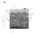
- 1 is an enlarged schematic schematic cross-sectional view of an underlying layer of an electronic component and its vicinity in an embodiment of the present invention; FIG. In the embodiment of the present invention, a TEM image of the cross section of the underlayer formed on the surface of the ceramic body (before plating) is shown.
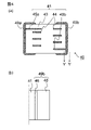
- 1(a) is a schematic schematic cross-sectional view of an exemplary electronic component in Example 1 of the present invention, and (b) is an enlarged schematic cross-sectional view along the YY plane of (a).
- FIG. 2 shows an STEM image of a cross section of the underlying layer in the sample produced in Example 1 of the present invention.
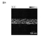
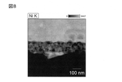
- FIG. 4 shows the result of investigating the distribution of Si by EDX analysis from a TEM image of the cross section of the underlying layer in the sample produced in Example 1 of the present invention. 4 shows the result of examining the distribution of Ag by EDX analysis from a TEM image of the cross section of the underlying layer in the sample produced in Example 1 of the present invention. 4 shows the result of examining the distribution of Ni by EDX analysis from a TEM image of the cross section of the underlying layer in the sample produced in Example 1 of the present invention. 1 shows an SEM image of the exposed surface (before plating) of the underlayer formed in Comparative Example 1 of the present invention. FIG.
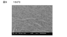
- FIG. 4 shows an SEM image of the exposed surface (before plating) of the underlayer formed in Example 2 of the present invention.
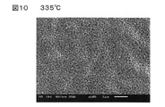
- FIG. FIG. 4 shows an SEM image of the exposed surface (before plating) of the underlayer formed in Example 3 of the present invention.
- FIG. FIG. 4 shows an SEM image of the exposed surface (before plating) of the underlayer formed in Example 4 of the present invention.
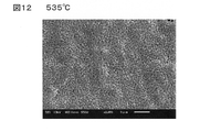
- FIG. FIG. 5 shows an SEM image of the exposed surface (before plating) of the underlayer formed in Example 5 of the present invention.
- FIG. FIG. 10 shows an SEM image of the exposed surface (before plating) of the underlayer formed in Example 6 of the present invention.
- FIG. FIG. 4 shows an SEM image of the exposed surface (before plating) of the underlayer formed in Comparative Example 2 of the present invention.
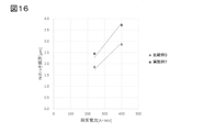
- FIG. 10 is a graph showing the Ni plating film thickness with respect to integrated current in Example 7 of the present invention and Comparative Example 3.
- FIG. 10 is a graph showing the Ni plating film thickness with respect to
- the electronic component of the present embodiment is an electronic component comprising a ceramic body and an external electrode provided on the surface of the ceramic body, the external electrode being a base layer in contact with the surface of the ceramic body. and a metal layer formed on the surface of the underlayer, the underlayer having pores communicating from the surface to the interface with the ceramic body, and part of the metal layer being , extends to the interface through the pores, and the voids in the underlayer are 1.5% by volume or less.
- the electronic component comprises a ceramic element body and external electrodes provided on the surface of the ceramic element body, the shape, size and material of the ceramic element body, the number, arrangement and shape of the external electrodes, etc. It is not particularly limited.
- the ceramic body may or may not have embedded internal electrodes, and if present, the internal electrodes are electrically connected to the external electrodes in a suitable manner.
- Electronic components that can be used in the present embodiment can be, for example, surface-mounted components, particularly chip components. (coils), resistors such as chip resistors, transistors, LC composites, and the like.
- the electronic component 10 of this embodiment can be a multilayer ceramic capacitor as shown in FIG. , 5b, and external electrodes 9a and 9b provided on the surface of the ceramic body 1 and electrically connected to the internal electrodes 5a and 5b, respectively. More specifically, the internal electrodes 5a and 5b are embedded in the ceramic body 1, laminated so as to be alternately exposed from the opposing end surfaces of the ceramic body 1, and electrically connected to the external electrodes 9a and 9b, respectively. ing.
- the electronic component 10 of the present embodiment is not limited to the one illustrated in FIG. 1(a), and may be various electronic components as described above.
- the external electrodes 9 are ceramic bodies 1 ( (mainly corresponding to the ceramic portion 3 illustrated in a)), and a metal layer 8 formed on the underlying layer 6 .
- the ceramic body 1 including the internal electrodes 5a and 5b shown in FIG. A metal layer 8 may be formed thereon.
- the material forming the metal layer 8 is not particularly limited as long as it is conductive, and examples thereof include nickel (Ni), copper (Cu), tin (Sn), and the like.
- the metal layer 8 may be a single layer or multiple layers.
- the thickness of the metal layer 8 is not particularly limited, but may be, for example, 100 nm or more and 10 ⁇ m or less.
- the metal layer 8 can include a nickel layer (Ni layer) in contact with the surface of the underlying layer 6 as a single layer, although this embodiment is not limited thereto.
- Ni layer nickel layer
- the metal layer 8 may be included as the innermost layer (the layer in contact with the surface of the ceramic body 1).
- the multi-layered metal layer 8 is a laminate (Ni/Cu/Sn layer) including a nickel layer (Ni layer), a copper layer (Cu layer) and a tin layer (Sn layer) in this order from the underlying layer 6. good.
- the nickel layer effectively prevents "solder erosion” in which the metal material contained in the underlying layer 6 is lost when an electronic component is soldered and mounted on a circuit board or the like (more specifically, on a land or the like). be able to.
- the tin layer can constitute the outermost layer of the external electrode 9, thereby improving "solder wettability" when mounting the electronic component on a circuit board or the like by soldering, and obtaining high strength at the solder joint. be able to.
- the copper layer can be appropriately provided according to the application of the electronic component.
- the underlayer 6 has pores P communicating from its surface 6a to the interface (back surface 6b) with the ceramic body 1.
- FIG. 2 shows the pores P communicating two-dimensionally (two-dimensionally) from the surface 6a to the back surface 6b, actually, inside the underlying layer 6, a large number of pores P are three-dimensionally (three-dimensionally) There are pores P, many of which communicate from the surface 6a to the back surface 6b. Therefore, it is difficult to directly confirm the communicating pores by image analysis.
- the underlying layer 6 is subjected to EDX analysis, and if an element (for example, Ni) that constitutes the metal layer 8 is present inside the underlying layer 6, it is found that the pores P are present there. I can guess.
- Ni element
- a part of the metal layer 8 passes through the pores P of the underlayer 6 and extends to the interface (back surface 6b) between the underlayer 6 and the ceramic body 1.
- the metal layer 8 extends over the entire thickness of the base layer 6 so as to extend the roots of a tree, so that the effect of anchoring the base layer 6 is high and the metal layer 8 is less likely to peel off.
- the voids in the underlying layer 6 are as low as 1.5% by volume or less.
- the term "void" means the space left after part of the metal layer 8 expands inside the pore P.
- a low porosity means that most of the pores P are filled with the metal layer 8 .
- the bonding strength between the underlying layer 6 and the metal layer 8 is further increased. That is, when the porosity is sufficiently low as 1.5% or less, the bonding strength between the underlying layer 6 and the metal layer 8 can be enhanced.
- the amount of voids (porosity) can be obtained by image analysis.
- the electronic component 10 is cut in the thickness direction of the base layer 6 into thin pieces, and the interface between the ceramic body 1 and the base layer 6 and the interface between the base layer 6 and the metal layer 8 are observed using TEM-EDX. After adjusting the position and direction of the sample so that the top is approximately horizontal, most of the image is the base layer 6, with a portion of the metal layer 8 on the front surface 6a side and the ceramic body 1 on the back surface 6b side. Enlarge so that part of the Next, all elements (except for carbon (C)) contained in the ceramic body 1, the underlayer 6 and the metal layer 8 are detected by EDX analysis, and each EDX image is synthesized and mapped. A threshold value is set so that a portion where no element is detected on the composite map becomes white, and binarization image processing is performed to obtain the area Sw of the white portion included inside the base layer 6 .
- the area of the entire underlying layer 6 is obtained on the same screen. On the screen, visually confirm the thickness of the base layer 6, select the thickest part, the thinnest part, and the middle thickness part, and lower the thickness at each position. The thickness of the formation 6 is measured.
- the average thickness Tave of the underlying layer 6 is obtained by averaging the three thickness measurements.
- the total length Ltotal of the base layer 6 is measured in the direction orthogonal to the visually determined thickness measurement direction. By multiplying the average thickness Tave of the underlayer 6 by the total length Ltotal, the total area Stotal of the underlayer 6 on the screen is obtained.
- the underlayer 6 preferably has a thickness of 0.1 ⁇ m or more and 2 ⁇ m or less.
- the thickness of the underlayer 6 is preferably 0.1 ⁇ m or more and 1.7 ⁇ m or less, more preferably 0.1 ⁇ m or more and 1.3 ⁇ m or less.
- Such a thin underlayer 6 can be formed by using a sol-gel method, for example.
- the thickness d T (see FIG. 2) of the underlayer 6 is understood as the distance between the ceramic body 1 and the metal layer 8 .
- the thickness of the underlayer 6 is measured at the central portion of the underlayer 6 using a cross-sectional image obtained by exposing a cross section in the thickness direction of the underlayer 6, observing the exposed cross section, and appropriately analyzing it as necessary. thickness.
- the above cross-sectional images are SEM images obtained using a scanning electron microscope (SEM), SIM images obtained using a scanning ion microscope (SIM), TEM images obtained using a transmission electron microscope (TEM), It may be an SEM/SIM/TEM-EDX image obtained by combining any of these with energy dispersive X-ray analysis (EDX).
- the exposed cross section may be obtained by processing an electronic component with a focused ion beam (FIB).
- the thickness of the underlying layer 6 is visually confirmed, and three portions, i.e., the thickest portion, the thinnest portion, and the intermediate thickness portion, are selected, and the respective positions are selected. , the thickness of the underlying layer 6 is measured. By averaging the measured values of the three thicknesses, the average thickness of the underlying layer 6 is obtained and defined as the thickness of the underlying layer 6 (corresponding to Tave described above).
- the base layer 6 may contain a base metal and glass. In the underlying layer 6, it can exist as a glass region 13 and an underlying metal region 11 (see FIG. 2).
- a portion A on the surface 6a side of the underlayer 6 (the interface side in contact with the metal layer 8) and a back surface 6b side of the underlayer 6 (in contact with the ceramic body 1) are shown. It is preferable that the area of the underlying metal region 11 within the range of the portion A is larger than the area of the underlying metal region 11 within the range of the portion B when compared with the portion B of the interface side where the substrate is located.
- the portion A of the base layer 6 closer to the metal layer 8 (the base layer 6
- the base metal/glass ratio in the portion B of the base layer 6 closer to the ceramic body 1 (the portion on the back surface 6b side of the base layer 6) is preferably higher than the base metal/glass ratio in the portion B (the portion on the back surface 6b side of the base layer 6).
- the “portion A closer to the metal layer 8 of the underlying layer 6” is defined by the thickness d A from the interface (surface 6a of the underlying layer 6) with the metal layer 8 of the underlying layer 6. refers to the part in
- the thickness d A can be appropriately set within a range of 50% or less of the thickness of the underlying layer 6 , and typically the thickness d A can be 30% of the thickness d T of the underlying layer 6 .
- “A portion B of the underlayer 6 closer to the ceramic body 1” is within a range defined by the thickness d B from the interface of the underlayer 6 with the ceramic body 1 (back surface 6b of the underlayer 6). It means part.
- the thickness d B should be equal to the thickness d A and may typically be 30% of the thickness d T of the underlayer 6 .
- a dense metal layer 8 can be formed by having a higher base metal/glass ratio in portion A of the base layer 6 than in portion B of the base layer 6 .
- the plated layer is formed on the surface of the conductive material (that is, the base metal region 11 of the base layer 6).
- the plated layer with sufficient density and thickness can be formed on the surface 6a of the base layer 6 when electroplating is performed (plating effect of improving the adhesion amount).
- the glass components tend to gather on the surface side of the underlayer (this is sometimes called "floating glass").
- the metal components are gathered on the surface 6a side of 6, which greatly differs from the conventional one.
- the underlayer metal/glass ratio of the underlayer 6 is large in the portion A located on the front surface 6a side and is located on the back surface 6b side. It can be made smaller at the portion B where it does.
- the base metal/glass ratio can be varied in the thickness direction of the base layer 6
- the sintered state of the glass formed by the sol-gel method and the metal salt It is presumed that the balance of the metallization state of the glass and the wettability between the glass and the metal have an effect.
- the "volume ratio of the metal to the glass (base metal/glass ratio)" can be specified as follows.
- the electronic component 10 is sliced in the thickness direction of the external electrode 9, and the base layer 6 of the external electrode 9 is photographed at an arbitrary position by TEM-EDX. Subsequently, an EDX image of the main component of the glass (for example, Si in the case of silica glass) and the main component of the underlying metal (for example, silver) is obtained.
- the range of width 650 nm is divided into 10 regions by dividing the thickness dT of the underlying layer 6 equally into 10 regions, and the regions are divided from the surface 6a side of the underlying layer 6 toward the back surface 6b side. numbered from 1 to 10.
- An image of a desired range (three areas No. 1 to No. 3 when the thickness dT is 30%) is cut out from the surface 6a side.
- a threshold value is set so that when the target element (Si) is present, the image becomes white, binarization image processing is performed, and the area of the white portion included in regions 1 to 3 is obtained.
- images of the same number of regions three regions of Nos.
- the thickness dT of the underlayer 6 is equally divided into 10 areas and divided into 10 areas, and from the surface 6a side of the underlayer 6 to the back surface 6b side, No. 1 to No. 10 Numbering.
- An image of a desired range from the surface 6a side (however, the same range as when the EDX image of the Si element was image-processed. In this example, 30% of the thickness dT , that is, three regions of Nos. 1 to 3). break the ice.
- a threshold value is set so that the target element (Ag) is white, and binarization image processing is performed to obtain the area of the white portion included in the regions No. 1 to No. 3.
- images of the same number of regions are cut out from the rear surface 6b side, and binarization image processing is performed in the same manner, and the area of the white portion included in the regions Nos. 7 to 10 is obtained.
- Ask for Those areas are the portion on the surface 6a side of the underlayer 6 (the portion A closer to the metal layer 8 of the underlayer 6) and the portion on the back surface 6b side of the underlayer 6 (the portion of the underlayer 6 closer to the ceramic body 1).
- B) is proportional to the content of the underlying metal in each.
- the area of Si and the area of Ag in the portion A on the front surface 6a side of the underlayer 6 are set to S1 and A1, respectively, and the area of Si and the area of Ag in the portion B on the back surface 6b side of the underlayer 6 are set to S2 and A2, respectively,
- the base metal/glass ratio is obtained by the following formulas (2) and (3).
- the base metal/glass ratio in the portion A of the base layer 6 closer to the metal layer 8 (on the surface 6a side of the base layer 6) is 50% or more, and electrolytic plating was performed to form the metal layer 8.
- a plated layer with higher density can be formed on the surface 6a of the underlayer 6 (effect of improving the amount of plating deposited). If the following formula (5) is satisfied, it can be confirmed that the base metal/glass ratio in the portion A is 50% (0.5) or more. A1/S1>0.5 (5)
- the underlying layer 6 includes an underlying metal region 11 made of an underlying metal and a glass region 13 made of glass. In a cross-sectional view as shown in FIG. Preferably, at least two base metal regions 11 and at least two glass regions 13 are alternately arranged.
- the electronic component 10 When the electronic component 10 is mounted, it is heated for solder reflow, and the thermal stress applied at that time may cause cracks in the underlying layer 6 . This is considered to be due to the coefficient of thermal expansion of the ceramic body 1 and the thermal expansion of the glass forming the matrix of the underlayer 6 .
- the concentration of stress due to thermal expansion on the glass regions 13 can be alleviated. The occurrence can be suppressed.
- the base metal is preferably silver.
- the underlying metal may be copper.
- the glass preferably contains silicon, titanium and zirconium atoms.
- the metal layer preferably contains one or more selected from the group consisting of nickel, copper, and tin.
- the electronic component 10 of this embodiment can be manufactured, for example, by the following method.
- the ceramic body 1 is prepared.
- the ceramic body 1 can be made by any suitable method.
- the ceramic material forming the ceramic body 1 is not particularly limited, and is not particularly limited as long as it is a ceramic material used for electronic components. Since the electronic component 10 exemplarily shown in FIG. 1(a) is a multilayer capacitor, the ceramic material is a dielectric material such as BaTiO 3 , CaTiO 3 , SrTiO 3 , CaZrO 3 , (BaSr)TiO 3 . , Ba( ZrTi )O3 and ( BiZn ) Nb2O7 .
- the material forming the internal electrodes 5a and 5b is not particularly limited as long as it is conductive, and examples thereof include Ag, Cu, Pt, Ni, Al, Pd, and Au. Ag, Cu, and Ni are preferable for the material forming the internal electrodes 5a and 5b.
- the ceramic material used in the present embodiment is not limited to the materials described above, and can be appropriately selected according to the type, configuration, etc. of the electronic component.
- the ceramic material may be a ferrite material containing Fe, Ni, Zn, Mn, Cu, or the like.
- the ceramic body may have coils instead of the internal electrodes.
- Such a coil may be, for example, pre-embedded in the ceramic body or wound around the ceramic body before or after forming the external electrodes, as long as it is finally electrically connected to the external electrodes.
- Base Layer 6 Formation of Base Layer 6 Next, a base layer 6 is formed in a predetermined region of the ceramic body 1 where the external electrode 9 is to be formed.
- the underlayer 6 can be formed by a thin film forming method using a solution.
- a sol-gel method, a MOD (metal organic compound decomposition method) method, a CSD (chemical solution deposition) method, and the like can be used as a method for forming a thin film. These methods are often treated synonymously.
- the term "sol-gel method” is used to encompass the narrow sense of "sol-gel method", MOD and CSD, unless otherwise specified. By using the sol-gel method, it is easy to form a thin film with a thickness of 0.1 ⁇ m or more and 2.0 ⁇ m or less.
- the raw material composition may be a liquid material (paste) in which a glass raw material (glass precursor), a base metal raw material (metal salt), and an organic polymer are dissolved or dispersed in a solvent.
- the glass precursor is a glass raw material, and any starting material that can form a glass matrix (glass region 13) may be used.
- Glass precursors include metal alkoxides, acetylacetonate complexes, acetates, and the like.
- these raw materials may be modified with functional groups such as long-chain alkyl groups and epoxy groups. Compounds that can be used as glass precursors are described below.
- metal alkoxide Elements capable of synthesizing metal alkoxides include Li, Be, B, C, Na, Mg, Al, Si, P, K, Ca, Sc, Ti, V, Cr, Mn, Fe, Co, Ni, Cu, Zn, Ga, Ge, As, Rb, Sr, Y, Zr, Nb, Mo, Cd, In, Sn, Sb, Cs, Ba, La, Ce, Pr, Nd, Pm, Sm, Eu, Gd, Tb, Dy, Ho, Er, Tm, Yb, Lu, Hf, Ta, W, Hg, Tl, Pb, Bi, Th, Pa, U, Pu. Alkoxides of these elements can be used as precursors for glasses.
- metal alkoxides that can be used as glass precursors are shown below.
- acetylacetonate complex Specific acetylacetonate complexes that can be used as glass precursors are illustrated below. Lithium acetylacetonate, Titanium(IV) oxyacetylacetonate, Titanium diisopropoxide bis(acetylacetonate), Zirconium(IV) trifluoroacetylacetonate, Zirconium(IV) acetylacetonate , aluminum acetylacetonate, aluminum (III) acetylacetonate, calcium (II) acetylacetonate, zinc (II) acetylacetonate, and other metal complexes of acetylacetonate.
- Acetate Specific acetates that can be used as glass precursors are exemplified below. Acetates such as zirconium acetate, zirconium(IV) acetate hydroxide, and basic aluminum acetate.
- additives for glass The glass contained in the underlayer 6 may contain additives (hereinafter referred to as "glass additives") as exemplified below. Additives can be mixed in the form of powders, microparticles or nanoparticles.
- Soda Ash (Sodium Carbonate Na2CO3 ), Sodium Hydrogen Carbonate ( NaHCO3 ) , Sodium Percarbonate ( 2Na2CO3.3H2O2 ), Sodium Sulfite ( Na2SO3 ), Sodium Hydrogen Sulfite ( NaHSO3 ) , sodium sulfate ( Na2SO4 ), sodium thiosulfate ( Na2S2O3 ), sodium nitrate ( NaNO3 ) , sodium sulfite ( NaNO2 ) and other oxoacid salts; sodium fluoride (NaF), chloride Halogen compounds such as sodium (NaCl), sodium bromide (NaBr) and sodium iodide (NaI); oxides such as sodium peroxide ( Na2O2 ) and sodium hydroxide (NaOH); hydroxides and hydrogenation Sodium (NaH), sodium sulfide ( Na2S), sodium hydrogen sulfide (NaHS), sodium silicate ( Na
- Calcium peroxide CaO2
- calcium hydroxide Ca(OH) 2
- calcium fluoride CaF2
- calcium chloride CaCl2.2H2O
- calcium bromide CaBr2.2H2O
- Inorganic salts such as calcium iodide (CaI 2 3H 2 O), calcium hydride (CaH 2 ), calcium carbide (CaC 2 ), calcium phosphide (Ca 3 P 2 ); calcium carbonate (CaCO 3 ), hydrogen carbonate Calcium (Ca( HCO3 ) 2 ), Calcium nitrate (Ca( NO3 ) 2.4H2O ), Calcium sulfate ( CaSO4.2H2O ), Calcium sulfite ( CaSO3 ) , Calcium silicate ( CaSiO3 or Ca 2 SiO 4 ), calcium phosphate (Ca 3 (PO 4 ) 2 ), calcium pyrophosphate (Ca 2 O 7 P 2 ), calcium hypochlorite (Ca[ClO)
- Lithium carbonate ( Li2CO3 ) lithium chloride (LiCl), lithium titanate ( Li2TiO3 ), lithium nitride ( Li3N ), lithium peroxide ( Li2O2 ), lithium citrate ( Li3C 6H5O7 ), lithium fluoride ( LiF), lithium hexafluorophosphate ( LiPF6 ), lithium acetate ( C2H3LiO2 ), lithium iodide ( LiI), lithium hypochlorite ( ClLiO ) , lithium tetraborate (Li 2 B 4 O 7 ), lithium bromide (LiBr), lithium nitrate (LiNO 3 ), lithium hydroxide (LiOH), lithium aluminum hydride (LiAlH 4 ), lithium triethylborohydride ( Li( C2H5 ) 3BH ) , lithium hydride (LiH), lithium amide ( LiNH2 ), lithium imide ( Li2NH ), lithium diisopropy
- boron triiodide (BI3), sodium cyanoborohydride ( NaBH3CN ), sodium borohydride (NaBH4), tetrafluoroboric acid ( HBF4 ), triethylborane ( ( CH3CH2 ) 3B ), Borax ( Na2B4O5 ( OH) 4.8H2O ), boric acid (B (OH)3 ) .
- the metal salt is a raw material of the underlying metal, and any starting material capable of producing the underlying metal region 11 may be used.
- Examples of metal salts include nitrates, carboxylates, and the like, and nitrates are preferably used.
- the metal in the metal salt is not particularly limited, and can be appropriately selected according to the metal material described above.
- the metal salt may be a single metal salt or a mixture of two or more metal salts.
- the metal salts may also be solvated, eg hydrated. When the underlying metal is silver, a silver salt is used as the metal salt.
- Silver salts include, for example, silver nitrate, silver azide, disilver monofluoride, silver monoxide, silver chloride, silver chlorate, silver perchlorate, silver chromate, silver acetate, silver oxide, silver cyanide, cyanic acid Silver, silver bromide, silver bromate, silver hydroxide, silver carbonate, silver thiocyanate, silver tetrafluoroborate, silver trifluoromethanesulfonate, silver fluoride, silver iodide, silver iodate, silver sulfide, silver sulfate , and silver phosphate are preferred. Silver nanoparticles can also be used instead of silver salts.
- Organic polymers are used to increase the viscosity of the raw material composition to make it pasty.
- organic polymers include acrylic (acrylic acid, methacrylic acid, or homopolymers or copolymers of their esters, specifically acrylic acid ester copolymers, methacrylic acid ester copolymers, acrylic acid ester-methacrylic acid ester copolymer, etc.), polyvinyl acetal (specifically, polyvinyl acetal, polyvinyl butyral, etc.), cellulose (specifically, hydroxypropylcellulose, cellulose ether, carboxymethylcellulose, acetylcellulose, acetylnitrocellulose, etc.), Polyvinyl alcohol-based, polyvinyl acetate-based, polyvinyl chloride, polypropylene carbonate-based, polyvinylpyrrolidone, and other homopolymers or copolymers may be mentioned, and at least one selected from these may be contained.
- Solvents are alcohol-based (specifically, ethanol vapor pressure 5.9 kPa, 2-propanol 4.3 kPa, 1-butanol 0.6 kPa, etc.), glycol ether-based (specifically, propylene glycol dimethyl ether 7.6 kPa, ethylene glycol dimethyl ether 6.4 kPa, etc.).
- solvents have a vapor pressure of 0.1 kPa or more at room temperature, and particularly preferably 0.5 kPa or more. They have a higher vapor pressure than other common solvents used in pastes.
- the solvents described in Patent Document 1 are 0.0053 kPa of butyl carbitol acetate and 0.013 Pa of ethyl carbitol. Therefore, by using such a solvent, a raw material composition in which the polymer is non-uniform can be obtained. This is because the solvent easily evaporates, and fluidity is quickly lost between application and drying. Note that if the paste dries too easily, the life of the paste will be shortened, so a solvent having a vapor pressure of less than 0.1 kPa may be appropriately mixed in consideration of productivity.
- this raw material composition is applied to a predetermined region of the ceramic body 1 and dried as described later, a coating film in which the polymers are unevenly dispersed can be obtained. When this coating film is heat-treated, the unevenly dispersed organic polymer is gasified, and the glass is then melted, thereby forming the base layer 6 having pores penetrating from the front surface to the back surface.
- the feedstock composition may include frit (and optionally glass additives), metal salts and solvents, as well as any suitable reactants and additives, and the like.
- a reactant for obtaining a compound having a structure represented by the formula -OMO- (M is a metal atom) as a main skeleton by reacting a metal alkoxide for example, water or an alkoxy group of a metal alkoxide is converted to a hydroxyl group. and hydroxy group-containing compounds that can be substituted for.
- additives include catalysts that promote such reactions, viscosity modifiers, pH modifiers, stabilizers, and the like.
- such a raw material composition is applied to a predetermined region of the ceramic body 1 and dried as appropriate to form a coating film derived from the raw material composition.
- the coating method is not particularly limited, and dipping, spraying, screen printing, brush coating, inkjet printing, and the like can be used. Drying is carried out such that most, preferably substantially all, of the solvent in the raw composition is removed. More specifically, drying can be carried out by heating the ceramic body coated with the raw material composition at, for example, 25 to 200° C. for 5 to 60 minutes.
- the heat treatment temperature and time may be, for example, 300° C. or higher and 900° C. or lower, for example, 10 to 60 minutes.
- the temperature of the heat treatment is preferably 300° C. or more and less than 835° C., and the base metal/glass ratio of the base layer 6 can be increased in the portion A on the front surface 6a side and decreased in the portion B on the back surface 6b side.
- the temperature of the heat treatment is more preferably 300° C. or higher and 800° C. or lower, and the base metal/glass ratio in the portion A on the surface 6a side of the base layer 6 can be 50% or more.
- the temperature of the heat treatment is particularly preferably 400° C. or higher and 750° C. or lower.
- the raw material composition is gelled to form the underlayer 6 as a sol-gel fired film. More specifically, as a result of the heat treatment, the glass matrix (glass region 13) is formed from the glass precursor, and the underlying metal region 11 is formed from the metal material formed from the metal salt.
- the underlayer 6 thus formed by the sol-gel method has pores P communicating from the front surface to the back surface (the interface with the ceramic body 1). Furthermore, such a base layer 6 is sufficiently thinner than a base layer formed using a conventional conductive paste, for example, a thin base layer 6 having a thickness of 0.1 ⁇ m or more and 2 ⁇ m or less can be formed.
- the base metal/glass ratio in the portion A of the base layer 6 closer to the metal layer 8 is the base metal/glass ratio in the portion B of the base layer 6 closer to the ceramic body 1. Underlayer 6 with a higher ratio can be formed (see FIG. 2). Therefore, when forming the metal layer 8 by electroplating, the metal film 8 (plating layer) with sufficient density and thickness can be formed on the surface 6 a of the underlying layer 6 .
- the metal layer 8 is preferably formed by electrolytic plating, and the metal material can be present at high density on the surface 6a side of the underlying layer 6.
- the plating solution can permeate the entire pores P of the underlying layer 6, a plating layer can be formed inside the pores P.
- the metal layer 8 can be formed on the surface of the underlayer 6, and a part of the metal layer 8 can reach the back surface 6b of the underlayer 6 (the interface with the ceramic body 1) through the pores P. can.
- the plating layer can be formed in most of the interior of the pores P, it is easy to reduce the voids within the underlying layer 6 to 1.5% by volume or less.
- Electroplating can be performed by immersing the ceramic body 1 on which the base layer 6 is formed in a plating solution (plating bath) and plating under predetermined conditions.
- the plating solution to be used and the conditions for the plating treatment can be appropriately selected according to the type of metal to be plated, the thickness of the plating film, and the like.
- the surface 6a of the base layer 6 is sufficiently coated with the metal when electroplating is performed.
- a plated layer having an appropriate density and thickness can be formed, and the adhesion of the metal layer 8 can be improved.
- the electronic component 10 of the present embodiment can be manufactured.
- ceramic bodies for laminated inductors were used on the assumption that the electronic components were laminated inductors, but these results also apply to other electronic components. .
- Example 1 Preparation of Ceramic Element Body 41 First, a ceramic element body 41 for the laminated inductor 40 was prepared (see FIG. 4(a)).
- the ceramic body 41 includes a ceramic portion 43 made of a ferrite material, a coil conductor 44 wound in a coil shape inside the ceramic portion 43, and lead portions (internal electrodes 45a and 45b) of the coil conductor 44. board.
- the ceramic body 41 with the coating film was subjected to heat treatment at 635° C. for 30 minutes in an air atmosphere (normal pressure) to form a base layer 46 derived from the coating film (see FIG. 4B). .
- a cross section of the sample of this example (temperature of heat treatment: 635°C) was observed using a SEM device.
- the thickness of the underlying layer 46 was 109 nm. While the thickness of the underlayer formed by using commercially available silver paste as the conductive paste can be about 10 ⁇ m, the underlayer 46 in the sample of the present example is thin to about 1/90th of that thickness. was able to transform
- the sample of this example ( Heat treatment temperature: 635° C.) was processed to expose a cross section in the thickness direction of the underlying layer 46, and the exposed cross section was observed and analyzed.
- the obtained STEM image is shown in FIG. 5, and the TEM-EDX images of Si, Ag and Ni are shown in FIGS. 6 to 8, respectively. 5 to 8, the internal electrodes 45a and 45b of the ceramic body 41 are on the lower side, and the Ni metal layer 48 is on the upper side.
- the area of the glass region (Si) in the underlayer 46 is It decreases toward the metal layer 48 side.
- the TEM-EDX image (Ag) of the underlying layer 46 shown in FIG. It increases toward the layer 48 side. Therefore, the base metal/glass ratio in the portion of the base layer 46 closer to the metal layer 48 is higher than the base metal/glass ratio in the portion of the base layer 46 closer to the ceramic body 41 (internal electrodes 45a, 45b). I found out.
- the internal electrodes 45a and 45b and the underlying metal regions are both made of Ag, but their interfaces could be clearly distinguished from the EDX of glass (Si).
- the Ni metal layer 48 Since a part of the Ni metal layer 48 reaches the interface with the ceramic element body 41 from the inside of the pores of the underlayer 46, the Ni metal layer 48 and the underlayer 46 are firmly bonded, and the Ni metal layer 48 It can be said that it is not easily separated from the base layer 46 (the bonding strength between the metal layer 48 and the base layer 46 is high).
- Examples 2-6, Comparative Examples 1-2 The surface of the ceramic body 41 was treated in the same manner as in Example 1, except that the raw material composition was prepared according to "other than Example 1" in Table 1, and the temperature of the heat treatment was set to the temperature shown in Table 2.
- a base layer 46 was formed on the substrate to obtain samples (Examples 2 to 6, Comparative Examples 1 and 2). SEM images of the exposed surface of the underlayer 46 obtained by heat treatment at each treatment temperature are shown in FIGS. 9 to 15.
- FIG. 9 to 15 SEM images of the exposed surface of the underlayer 46 obtained by heat treatment temperature are shown in FIGS. 9 to 15.
- the electrical resistance of the sample was measured by applying the adjusted paste on the ceramic substrate by spin coating, firing it, and measuring it with a digital multimeter at a distance of 0.5 mm between the terminals. As the air gap decreased, the electrical resistance decreased.
- the Ni metal layer 48 is formed on the surface of the base layer 46 and then processed. A section in the thickness direction of the stratum 46 was exposed, and an STEM image and a TEM-EDX image of the exposed section were observed and specified.
- the porosity of the underlayer 46 was obtained.
- the porosity was obtained by the method described above.
- the elements subjected to EDX analysis are oxygen (O), aluminum (Al), silicon (Si), titanium (Ti), iron (Fe), nickel (Ni), zinc (Zn), zirconium (Zr), silver (Ag) and tin (Sn).
- the adhesion between the base layer and the metal layer was evaluated as follows. A Ni metal layer 48 was formed on the surface of the underlying layer 46 . Thereafter, the surface of the metal layer 48 was adhered to the surface of the test substrate with an adhesive using the surface of the metal layer 48 as the adhesion surface. Next, the sample is pressed in a direction parallel to the surface of the test substrate (that is, a shearing force is applied), and the pressure (shearing force) at which the metal layer 48 is peeled off from the underlying layer 46 is determined, and the peeling strength ( N) was confirmed. A peel strength of 5 N or less was evaluated as NG (x), and a peel strength of 5 N or more was evaluated as G ( ⁇ ).
- Example 7 Comparative Example 3
- Comparative Example 3 is a common silver paste (73 wt% Ag particles, 4 wt% glass frit (ZnO—B 2 O 3 —SiO 2 ), 10 wt% ethyl cellulose, 1:1 mixture of butyl carbitol acetate and ethyl carbitol).
- Ni plating was performed on the base electrode formed using the liquid 13 wt %.
- the film thickness of the Ni plating film (Ni metal layer 48) in Example 7 is larger than that of the plating film in Comparative Example 3. all right. From this, it was found that Example 7 has a large base metal/glass ratio.
- Reference Signs List 1 41 ceramic element 3, 43 ceramic portion 5a, 5b, 45a, 45b internal electrode 6, 46 base layer 8, 48 metal layer 9, 9a, 9b, 49a, 49b external electrode 10 electronic component (multilayer ceramic capacitor) 11 base metal region 13 glass region 40 electronic component (laminated inductor) 44 coil conductor
Landscapes
- Engineering & Computer Science (AREA)
- Power Engineering (AREA)
- Microelectronics & Electronic Packaging (AREA)
- Manufacturing & Machinery (AREA)
- Chemical & Material Sciences (AREA)
- Materials Engineering (AREA)
- Fixed Capacitors And Capacitor Manufacturing Machines (AREA)
Abstract
外部電極が下地層および金属層を含み、下地層と金属層との密着性に優れた電子部品を提供する。セラミック素体と、該セラミック素体の表面に設けられた外部電極とを備える電子部品であって、該外部電極は、前記セラミック素体の表面に接触する下地層と、該下地層の表面上に形成された金属層とを含み、前記下地層は、その表面から、前記セラミック素体との界面まで連通する細孔を有し、前記金属層の一部は、前記細孔内を通って前記界面まで延在しており、前記下地層内の空隙は1.5体積%以下である、電子部品。
Description
本発明は、電子部品およびその製造方法に関し、より詳細には、セラミック素体と、該セラミック素体の表面に設けられた外部電極とを備える電子部品およびその製造方法に関する。
電子部品は、回路基板等に実装するための外部電極を備え得る。従来の一般的な電子部品において、外部電極は、導電性ペーストをセラミック素体に塗布および焼成して、導電性ペーストに由来する下地層を形成し、この下地層にめっきを施すことにより形成されている。
積層チップインダクタの外部電極は、多数の細孔を有した多孔質の部材からなる。例えば特許文献1には、外部電極の多孔度(気孔率)について10%~30%程度が望ましいこと、細孔の平均孔径は0.3μm~4.0μmが望ましいことが記載されている。この細孔には、焼結体と内部電極との間に介在させた緩衝材と同一物質の樹脂が含浸されている。外部電極の表層には、メッキ層が形成されている。
外部電極は焼成により形成され、焼成後に多数の細孔が生じるような組成のものから形成される。例えば、Ag粒子(球状粒子,平均粒径0.5μm)が73wt%,ガラスフリット(ZnO-B2O3-SiO2)が4wt%,エチルセルロースが10wt%,ブチルカルビトールアセテートとエチルカルビトールとの1:1混合液が13wt%からなるAgを主成分とする金属ペーストを用いることにより、焼成時にガラスフリットがガス化して多孔質の金属部材が形成されると記載されている。
特許文献1では、多孔質の外部電極(下地層)とめっき層(金属層)との結合力が十分ではなく、特に電子部品が小型化すると金属層が剥離するおそれがあった。
そこで本発明は、セラミック素体および外部電極を備える電子部品であって、外部電極が下地層および金属層を含み、下地層と金属層との密着性に優れた電子部品を提供すること、およびその製造方法を提供することを目的とする。
そこで本発明は、セラミック素体および外部電極を備える電子部品であって、外部電極が下地層および金属層を含み、下地層と金属層との密着性に優れた電子部品を提供すること、およびその製造方法を提供することを目的とする。
本発明の1つの要旨によれば、
セラミック素体と、該セラミック素体の表面に設けられた外部電極とを備える電子部品であって、
該外部電極は、前記セラミック素体の表面に接触する下地層と、該下地層の表面上に形成された金属層とを含み、
前記下地層は、その表面から、前記セラミック素体との界面まで連通する細孔を有し、
前記金属層の一部は、前記細孔内を通って前記界面まで延在しており、
前記下地層内の空隙は1.5体積%以下である電子部品が提供される。
セラミック素体と、該セラミック素体の表面に設けられた外部電極とを備える電子部品であって、
該外部電極は、前記セラミック素体の表面に接触する下地層と、該下地層の表面上に形成された金属層とを含み、
前記下地層は、その表面から、前記セラミック素体との界面まで連通する細孔を有し、
前記金属層の一部は、前記細孔内を通って前記界面まで延在しており、
前記下地層内の空隙は1.5体積%以下である電子部品が提供される。
本発明の別の要旨によれば、
セラミック素体と、該セラミック素体の表面に設けられた外部電極とを備える電子部品を製造する方法であって、
該外部電極は、前記セラミック素体の表面に接触する下地層と、該下地層の表面上に形成された金属層とを含み、前記下地層は下地金属とガラスとを含み、
前記方法は、
前記ガラスの原料となるガラス前駆体と、前記下地金属の原料となる金属塩と、増粘剤である有機高分子と、室温における蒸気圧が0.1kPa以上の溶媒とを含む原料組成物を調製し、当該原料組成物を前記セラミック素体の表面に塗布した後に加熱処理して下地層を形成する工程と、
前記下地層の表面に、電解めっきにより前記金属層を形成する工程とを含む、電子部品の製造方法が提供される。
セラミック素体と、該セラミック素体の表面に設けられた外部電極とを備える電子部品を製造する方法であって、
該外部電極は、前記セラミック素体の表面に接触する下地層と、該下地層の表面上に形成された金属層とを含み、前記下地層は下地金属とガラスとを含み、
前記方法は、
前記ガラスの原料となるガラス前駆体と、前記下地金属の原料となる金属塩と、増粘剤である有機高分子と、室温における蒸気圧が0.1kPa以上の溶媒とを含む原料組成物を調製し、当該原料組成物を前記セラミック素体の表面に塗布した後に加熱処理して下地層を形成する工程と、
前記下地層の表面に、電解めっきにより前記金属層を形成する工程とを含む、電子部品の製造方法が提供される。
本発明によれば、セラミック素体および外部電極を備える電子部品であって、外部電極が下地層および金属層を含み、下地層と金属層との密着性に優れた電子部品が提供される。また、本発明によれば、そのような電子部品の製造方法が提供される。
本実施形態の電子部品は、セラミック素体と、該セラミック素体の表面に設けられた外部電極とを備える電子部品であって、該外部電極は、前記セラミック素体の表面に接触する下地層と、該下地層の表面上に形成された金属層とを含み、前記下地層は、その表面から、前記セラミック素体との界面まで連通する細孔を有し、前記金属層の一部は、前記細孔内を通って前記界面まで延在しており、前記下地層内の空隙は1.5体積%以下である。
電子部品は、セラミック素体と、該セラミック素体の表面に設けられた外部電極とを備えるものであれば、セラミック素体の形状、寸法および材料、ならびに外部電極の数、配置および形状等は特に限定されない。セラミック素体は内部電極を埋設していても、いなくてもよく、存在する場合には内部電極は外部電極に適切な態様で電気的に接続される。
本実施形態に利用可能な電子部品は、例えば表面実装型、特にチップ部品であり得、より詳細には、積層セラミックコンデンサ等のコンデンサ(キャパシタ)、巻線インダクタ、フィルムインダクタ、積層インダクタ等のインダクタ(コイル)、チップ抵抗器等の抵抗器、トランジスタ、LC複合部品などであり得る。
例示的には、本実施形態の電子部品10は、図1(a)に示すような積層セラミックコンデンサであり得、セラミック材料からなるセラミック部3およびセラミック部3を介して互いに対向する内部電極5a、5bを含むセラミック素体1と、セラミック素体1の表面に設けられ、かつ内部電極5a、5bとそれぞれ電気的に接続された外部電極9a、9bとを備える。より詳細には、内部電極5a、5bは、セラミック素体1に埋設され、セラミック素体1の対向する端面から交互に露出するように積層され、それぞれ外部電極9a、9bと電気的に接続されている。しかしながら、本実施形態の電子部品10は、図1(a)に例示するものに限定されず、上述したような種々の電子部品であり得る。
本実施形態の電子部品10において、図1(b)に示すように、外部電極9(図1(a)に例示する外部電極9a、9bに対応する)は、セラミック素体1(図1(a)に例示するセラミック部3に主に対応する)の表面に接触する下地層6と、下地層6上に形成された金属層8とを含む。なお、図1(a)に示す内部電極5a、5bを含むセラミック素体1では、セラミック素体1の端面から露出した内部電極5a、5bと接するように下地層6を形成し、下地層6上に金属層8を形成し得る。
金属層8を構成する材料は、導電性であれば特に限定されず、例えばニッケル(Ni)、銅(Cu)、スズ(Sn)等が挙げられる。金属層8は、単層であっても、多層であってもよい。金属層8の厚さは、特に限定されないが、例えば100nm以上10μm以下であり得る。
本実施形態を限定するものではないが、より詳細には、金属層8は、下地層6の表面と接触するニッケル層(Ni層)を単層で含むことができる。
金属層8が多層の場合、最内層(セラミック素体1の表面に接触する層)として含み得る。例えば、多層の金属層8は、ニッケル層(Ni層)、銅層(Cu層)およびスズ層(Sn層)を下地層6からこの順に含む積層体(Ni/Cu/Sn層)であってよい。
金属層8が多層の場合、最内層(セラミック素体1の表面に接触する層)として含み得る。例えば、多層の金属層8は、ニッケル層(Ni層)、銅層(Cu層)およびスズ層(Sn層)を下地層6からこの順に含む積層体(Ni/Cu/Sn層)であってよい。
ニッケル層は、電子部品を回路基板等(より詳細にはランド等)にはんだ付けして実装する際に下地層6に含まれる金属材料が喪失するという「はんだ食われ」を効果的に防止することができる。スズ層は、外部電極9の最外層を構成し得、これにより、電子部品を回路基板等にはんだ付けにより実装する際に「はんだ濡れ性」が良好になり、はんだ接合部において高い強度を得ることができる。銅層は、電子部品の用途に応じて適宜設けられ得る。
図2に示すように、下地層6は、その表面6aから、セラミック素体1との界面(裏面6b)まで連通する細孔Pを有している。図2では平面的(二次元的)に表面6aから裏面6bまで連通する細孔Pを示しているが、実際には下地層6の内部には、立体的(三次元的)に、多数の細孔Pが存在し、その多くが表面6aから裏面6bまで連通している。そのため、連通する細孔を画像解析で直接的に確認することは難しい。金属層8を形成した後に下地層6をEDX分析し、金属層8を構成する元素(例えばNi)が下地層6の内部に存在している場合には、そこに細孔Pが存在していたと推測できる。なお、下地層6の表面6aに金属層8を形成すると、その細孔内にも金属層8の一部が形成されるため、最終製品の電子部品10では、細孔Pの多くは空隙としては残らない。
金属層8の一部は、下地層6の細孔P内を通って、下地層6とセラミック素体1との界面(裏面6b)まで延在している。これにより、金属層8は、木の根を張り巡らせるように下地層6の厚さ全体にわたって延在するので、下地層6に対するアンカー効果が高く、金属層8が剥離しにくいという効果を奏する。
本実施形態では、下地層6内の空隙は1.5体積%以下と低い。本明細書では「空隙」とは、細孔Pの内部に金属層8の一部が広がった後に残った空間のことを意味する。
空隙率が低いことは、細孔Pの大部分が金属層8で満たされていることを意味している。細孔Pの大部分が金属層8で満たされていると、下地層6と金属層8との結合力がさらに高まる。つまり、空隙率が1.5%以下と十分に低いと、下地層6と金属層8との結合力を高めることができる。
空隙率が低いことは、細孔Pの大部分が金属層8で満たされていることを意味している。細孔Pの大部分が金属層8で満たされていると、下地層6と金属層8との結合力がさらに高まる。つまり、空隙率が1.5%以下と十分に低いと、下地層6と金属層8との結合力を高めることができる。
空隙の量(空隙率)は、画像解析により求めることができる。電子部品10を、下地層6の厚さ方向に切断、薄片化し、TEM-EDXにて、セラミック素体1と下地層6との界面、および下地層6と金属層8との界面が観察画面上でおおよそ水平方向となるように試料の位置および方向を調整後、画像の大部分が下地層6で、その表面6a側に金属層8の一部と、その裏面6b側にセラミック素体1の一部が写るように拡大する。次いで、セラミック素体1、下地層6および金属層8に含まれる全ての元素(炭素(C)を除く)をEDX分析により検出し、各EDX像を合成マップ化する。合成マップ上で元素が検出されない部分が白色となるように閾値を設定して2値化の画像処理を行い、下地層6内部に含まれる白色部分の面積Swを求める。
同じ画面上で、下地層6全体の面積を求める。画面上で、下地層6の厚さを目視で確認して、最も厚いと思われる部分、最も薄いと思われる部分、その中間の厚さの部分の3カ所を選択し、それぞれの位置で下地層6の厚さを測定する。3つの厚さの測定値を平均して、下地層6の平均厚さTaveを求める。
同じ画面上で、目視により決定した厚さの測定方向と直交する方向における、下地層6の全長Ltotalを測定する。下地層6の平均厚さTaveと全長Ltotalを掛けて、画面上における下地層6の総面積Stotalを求める。
白色部分の面積Swを、下地層6の総面積Stotalで割ることにより、空隙率を算出する。つまり、空隙率は下式(1)で求めることができる。
空隙率(%)=Sw/(Ltotal×Tave)×100
=Sw/Stotal×100・・・(1)
同じ画面上で、目視により決定した厚さの測定方向と直交する方向における、下地層6の全長Ltotalを測定する。下地層6の平均厚さTaveと全長Ltotalを掛けて、画面上における下地層6の総面積Stotalを求める。
白色部分の面積Swを、下地層6の総面積Stotalで割ることにより、空隙率を算出する。つまり、空隙率は下式(1)で求めることができる。
空隙率(%)=Sw/(Ltotal×Tave)×100
=Sw/Stotal×100・・・(1)
なお、白色部分の面積Swを求める際の2値化のための閾値の設定が難しい場合は、EDX像を視認して、元素が検出できない領域(白っぽく表示される)の形状を識別し、それらの輪郭を手書きでなぞって、各々の面積を算出してもよい。
下地層6は、厚さが0.1μm以上2μm以下であることが好ましい。下地層6の厚さがこの範囲にあると、金属層8とセラミック素体1との結合力を向上する効果を十分に発揮でき、また、金属層8の一部が下地層6の細孔Pを通って下地層6とセラミック素体1との界面(下地層6の裏面6b)まで到達することが容易になる。
下地層6の厚さは、好ましくは0.1μm以上1.7μm以下であり、より好ましくは0.1μm以上1.3μm以下である。
このような薄い下地層6は、例えばゾル-ゲル法を用いることで形成することができる。
下地層6の厚さは、好ましくは0.1μm以上1.7μm以下であり、より好ましくは0.1μm以上1.3μm以下である。
このような薄い下地層6は、例えばゾル-ゲル法を用いることで形成することができる。
下地層6の厚さdT(図2参照)は、セラミック素体1と金属層8との間の距離として理解される。下地層6の厚さは、下地層6の厚さ方向断面を露出させ、その露出断面を観察および必要に応じて適宜分析して得られる断面像を使用して、下地層の中央部において測定した厚さとして求められ得る。上記断面像は、走査電子顕微鏡(SEM)を使用して得られるSEM像、走査イオン顕微鏡(SIM)を使用して得られるSIM像、透過電子顕微鏡(TEM)を使用して得られるTEM像、これらのいずれかをエネルギー分散型X線分析(EDX)と組み合わせて得られるSEM/SIM/TEM-EDX像などであってよい。上記露出断面は、電子部品を集束イオンビーム(FIB)により加工したものであってもよい。
適切な断面像において、下地層6の厚さを目視で確認して、最も厚いと思われる部分、最も薄いと思われる部分、その中間の厚さの部分の3カ所を選択し、それぞれの位置で下地層6の厚さを測定する。3つの厚さの測定値を平均して、下地層6の平均厚さを求めて下地層6の厚さ(上述したTaveに相当)とする。
下地層6は、下地金属とガラスとを含んでもよい。下地層6において、ガラス領域13と下地金属領域11として存在し得る(図2参照)。下地層6の断面視(図2)において、下地層6の表面6a側(金属層8と接している界面側)の部分Aと、下地層6の裏面6b側(セラミック素体1と接している界面側)の部分Bとを比較したときに、部分Aの範囲内における下地金属領域11の面積が、部分Bの範囲内における下地金属領域11の面積よりも大きいことが好ましい。これを、「ガラスに対する前記下地金属の体積比」(本明細書では「下地金属/ガラス比」と称することがある)として比較すると、下地層6の金属層8により近い部分A(下地層6の表面6a側の部分)における下地金属/ガラス比は、下地層6のセラミック素体1により近い部分B(下地層6の裏面6b側の部分)における下地金属/ガラス比より高いことが好ましい。
本明細書において「下地層6の金属層8により近い部分A」とは、下地層6の金属層8との界面(下地層6の表面6a)から、厚さdAで規定される範囲内にある部分のことをいう。厚さdAは、下地層6の厚さの50%以下の範囲で適宜設定され得、典型的には、厚さdAは下地層6の厚さdTの30%であり得る。
「下地層6のセラミック素体1により近い部分B」とは、下地層6のセラミック素体1との界面(下地層6の裏面6b)から、厚さdBで規定される範囲内にある部分のことをいう。厚さdBは、厚さdAと等しい厚さとし、典型的には、下地層6の厚さdTの30%であり得る。
「下地層6のセラミック素体1により近い部分B」とは、下地層6のセラミック素体1との界面(下地層6の裏面6b)から、厚さdBで規定される範囲内にある部分のことをいう。厚さdBは、厚さdAと等しい厚さとし、典型的には、下地層6の厚さdTの30%であり得る。
下地層6の部分Aにおける下地金属/ガラス比が、部分Bにおける下地金属/ガラス比より高いことにより、密度の高い金属層8を形成し得る。
電解めっきで金属層8を形成するとき、めっき層は導電性材料(つまり、下地層6の下地金属領域11)の表面に形成される。下地層6の表面6a側に下地金属領域11が多く存在すると、電解めっきを行ったときに、下地層6の表面6aに十分な密度と厚さのめっき層を形成することができる(めっきの付着量の向上効果)。
電解めっきで金属層8を形成するとき、めっき層は導電性材料(つまり、下地層6の下地金属領域11)の表面に形成される。下地層6の表面6a側に下地金属領域11が多く存在すると、電解めっきを行ったときに、下地層6の表面6aに十分な密度と厚さのめっき層を形成することができる(めっきの付着量の向上効果)。
通常、下地金属とガラスを含む下地層を形成すると、下地層の表面側にガラス成分が集まる傾向がある(これを「ガラスが浮く」と呼ぶことがある)が、本実施形態では、下地層6の表面6a側に金属成分が集まっている点で、従来と大きく異なる。
本実施の形態では、下地層6を形成するときの加熱処理の温度を制御することにより、下地層6の下地金属/ガラス比を表面6a側に位置する部分Aで大きく、裏面6b側に位置する部分Bで小さくすることができる。なお、下地金属/ガラス比を下地層6の厚さ方向で異ならせることができるメカニズムは定かではないが、下地層6の形成時に、ゾル-ゲル法で形成したガラスの焼結状態と金属塩の金属化状態のバランス、ガラスと金属との濡れ性などが影響していると推測される。
本実施の形態では、下地層6を形成するときの加熱処理の温度を制御することにより、下地層6の下地金属/ガラス比を表面6a側に位置する部分Aで大きく、裏面6b側に位置する部分Bで小さくすることができる。なお、下地金属/ガラス比を下地層6の厚さ方向で異ならせることができるメカニズムは定かではないが、下地層6の形成時に、ゾル-ゲル法で形成したガラスの焼結状態と金属塩の金属化状態のバランス、ガラスと金属との濡れ性などが影響していると推測される。
「前記ガラスに対する前記金属の体積比(下地金属/ガラス比)」は、次のように特定することができる。
電子部品10を外部電極9の厚さ方向に切断、薄片化し、TEM-EDXにて外部電極9の下地層6を任意の位置で撮影する。続いてガラスの主成分(例えば、シリカガラスであれはSi)と下地金属の主成分(例えば、銀)のEDX像をそれぞれ取得する。
電子部品10を外部電極9の厚さ方向に切断、薄片化し、TEM-EDXにて外部電極9の下地層6を任意の位置で撮影する。続いてガラスの主成分(例えば、シリカガラスであれはSi)と下地金属の主成分(例えば、銀)のEDX像をそれぞれ取得する。
次に、Si元素のEDX像上で、幅650nmの範囲について、下地層6の厚さdTを10等分して10領域に区分し、下地層6の表面6a側から裏面6b側に向かって1番~10番までナンバリングする。表面6a側から所望の範囲(厚さdTの30%とする場合は、1番~3番の3領域)の画像を切り出す。対象となる元素(Si)が存在する場合に白色となるように閾値を設定して2値化の画像処理を行い、領域1番~3番に含まれる白色部分の面積を求める。次に、裏面6b側から同数の領域(7番~10番の3領域)の画像を切り出して、同様に2値化の画像処理を行い、領域7番~10番に含まれる白色部分の面積を求める。それらの面積は、下地層6の表面6a側の部分(下地層6の金属層8により近い部分A)と、下地層6の裏面6b側の部分(下地層6のセラミック素体1により近い部分B)の各々におけるガラスの含有量に比例する。
そして、Ag元素のEDX像上で、下地層6の厚さdTを10等分して10領域に区分し、下地層6の表面6a側から裏面6b側に向かって1番~10番までナンバリングする。表面6a側から所望の範囲(但し、Si元素のEDX像について画像処理した時と同じ範囲にする。この例では厚さdTの30%、つまり1番~3番の3領域)の画像を切り出す。対象となる元素(Ag)が存在する場合に白色となるように閾値を設定して2値化の画像処理を行い、領域1番~3番に含まれる白色部分の面積を求める。次に、裏面6b側から同数の領域(7番~10番の3領域)の画像を切り出して、同様に2値化の画像処理を行い、領域7番~10番に含まれる白色部分の面積を求める。それらの面積は、下地層6の表面6a側の部分(下地層6の金属層8により近い部分A)と、下地層6の裏面6b側の部分(下地層6のセラミック素体1により近い部分B)の各々における下地金属の含有量に比例する。
なお、2値化のための閾値の設定が難しい場合は、EDX像を視認して、下地金属領域11とガラス領域13の形状を識別し、それらの輪郭を手書きでなぞって、各々の面積を算出してもよい。
下地層6の表面6a側の部分AにおけるSiの面積とAgの面積をそれぞれS1、A1とし、下地層6の裏面6b側の部分BにおけるSiの面積とAgの面積をそれぞれS2、A2として、以下の式(2)、(3)で下地金属/ガラス比を求める。
「下地層6の金属層8により近い部分Aにおけるガラスに対する下地金属の体積比」、つまり、下地層6の表面6a側の部分Aにおける下地金属/ガラス比=A1/S1・・・(2)
「下地層6のセラミック素体1により近い部分Bにおけるガラスに対する下地金属の体積比」つまり下地層6の裏面6b側の部分Bにおける下地金属/ガラス比=A2/S2・・・(3)
そして、下式(4)を満たせば、部分Aにおける下地金属/ガラス比が部分Bにおける下地金属/ガラス比より大きいことが確認できる。
A1/S1>A2/S2・・・(4)
「下地層6の金属層8により近い部分Aにおけるガラスに対する下地金属の体積比」、つまり、下地層6の表面6a側の部分Aにおける下地金属/ガラス比=A1/S1・・・(2)
「下地層6のセラミック素体1により近い部分Bにおけるガラスに対する下地金属の体積比」つまり下地層6の裏面6b側の部分Bにおける下地金属/ガラス比=A2/S2・・・(3)
そして、下式(4)を満たせば、部分Aにおける下地金属/ガラス比が部分Bにおける下地金属/ガラス比より大きいことが確認できる。
A1/S1>A2/S2・・・(4)
下地層6の金属層8により近い部分A(下地層6の表面6a側)における下地金属/ガラス比が50%以上であることが特に好ましく、金属層8の形成のために電解めっきを行ったときに、下地層6の表面6aに、より密度が高いめっき層を形成することができる(めっきの付着量の向上効果)。
下式(5)を満たせば、部分Aにおける下地金属/ガラス比が50%(0.5)以上であることが確認できる。
A1/S1>0.5・・・(5)
下式(5)を満たせば、部分Aにおける下地金属/ガラス比が50%(0.5)以上であることが確認できる。
A1/S1>0.5・・・(5)
下地層6は下地金属からなる下地金属領域11とガラスからなるガラス領域13とを含み、図3に示すような断面視において、下地層6の厚さ方向に沿って引いた直線L上に、少なくとも2つの下地金属領域11と少なくとも2つのガラス領域13が交互に配置されていることが好ましい。
電子部品10の実装時にはんだリフローのために加熱するが、そのときにかかる熱応力によって下地層6にクラックが発生することがある。これは、セラミック素体1の熱膨張率と、下地層6のマトリクスを構成するガラスとの熱膨張に起因すると考えられる。下地層6の厚さ方向に沿って、ガラス領域13と下地金属領域11とを交互に配置すると、ガラス領域13に熱膨張による応力が集中することを緩和でき、その結果、リフロー時のクラックの発生を抑制することができる。
電子部品10の実装時にはんだリフローのために加熱するが、そのときにかかる熱応力によって下地層6にクラックが発生することがある。これは、セラミック素体1の熱膨張率と、下地層6のマトリクスを構成するガラスとの熱膨張に起因すると考えられる。下地層6の厚さ方向に沿って、ガラス領域13と下地金属領域11とを交互に配置すると、ガラス領域13に熱膨張による応力が集中することを緩和でき、その結果、リフロー時のクラックの発生を抑制することができる。
下地金属は銀であるのが好ましい。また、下地金属は銅であってもよい。ガラスはケイ素原子、チタン原子およびジルコニウム原子を含むことが好ましい。また、金属層はニッケル、銅、スズからなる群から選択される1種以上を含むことが好ましい。
[製造方法]
本実施形態の電子部品10は、例えば以下の方法により製造可能である。
本実施形態の電子部品10は、例えば以下の方法により製造可能である。
1)セラミック素体1の準備
まず、セラミック素体1を準備する。セラミック素体1は、任意の適切な方法により作製され得る。
まず、セラミック素体1を準備する。セラミック素体1は、任意の適切な方法により作製され得る。
例えば、セラミック素体1(より詳細にはセラミック部3)を構成するセラミック材料は、特に限定されず、電子部品に用いられるセラミック材料であれば特に限定されない。図1(a)に例示的に示した電子部品10は積層コンデンサであるので、セラミック材料は、誘電体材料であり、例えば、BaTiO3、CaTiO3、SrTiO3、CaZrO3、(BaSr)TiO3、Ba(ZrTi)O3および(BiZn)Nb2O7等が挙げられる。存在する場合、内部電極5a、5bを構成する材料は、導電性であれば特に限定されず、例えば、Ag、Cu、Pt、Ni、Al、Pd、Au等が挙げられる。内部電極5a、5bを構成する材料は、Ag、Cu、及びNiが好ましい。
なお、本実施形態に用いられるセラミック材料は、上記した材料に限定されず、電子部品の種類、構成等に応じて適宜選択され得る。例えば、電子部品が、フェライトコイル部品である場合には、セラミック材料は、Fe、Ni、Zn、Mn、Cu等を含むフェライト材料であってもよい。この場合、セラミック素体は、内部電極の代わりに、コイルを備えていればよい。かかるコイルは、最終的に外部電極に電気的に接続される限り、例えばセラミック素体に予め埋設されていても、外部電極を形成する前または後にセラミック素体の周囲に巻き付けられてもよい。
2)下地層6の形成
次に、セラミック素体1の外部電極9を形成すべき所定の領域に下地層6を形成する。
次に、セラミック素体1の外部電極9を形成すべき所定の領域に下地層6を形成する。
本実施形態では、下地層6は、溶液を用いた薄膜作製法にて形成し得る。薄膜作製法としては、ゾル-ゲル法、MOD(金属有機化合物分解法)法、CSD(chemical solution deposition)法などが利用できる。なお、これらの方法は同義に扱われることが多い。本明細書で使用する「ゾル-ゲル法」の用語は、特に説明がない限り、狭義の「ゾル-ゲル法」、MODおよびCSDを包含するものとして使用する。
ゾル-ゲル法を用いると、厚さ0.1μm以上2.0μm以下の薄膜を形成することが容易である。
ゾル-ゲル法を用いると、厚さ0.1μm以上2.0μm以下の薄膜を形成することが容易である。
ゾル-ゲル法を用いて下地層6を形成する場合、下地層6を形成するための原料組成物を準備する。原料組成物は、ガラスの原料(ガラスの前駆体)、下地金属の原料(金属塩)、および有機高分子が溶媒中に溶解または分散した液状物(ペースト)であってもよい。
[ガラスの前駆体]
ガラスの前駆体はガラス原料であり、ガラスのマトリクス(ガラス領域13)を生じ得る出発原料であればよい。ガラスの前駆体としては、金属アルコキシド、アセチルアセトナート錯体、酢酸塩等が挙げられる。また、それらの原料は、長鎖アルキル基やエポキシ基等の官能基で修飾されていてもよい。以下に、ガラスの前駆体として使用し得る化合物について説明する。
ガラスの前駆体はガラス原料であり、ガラスのマトリクス(ガラス領域13)を生じ得る出発原料であればよい。ガラスの前駆体としては、金属アルコキシド、アセチルアセトナート錯体、酢酸塩等が挙げられる。また、それらの原料は、長鎖アルキル基やエポキシ基等の官能基で修飾されていてもよい。以下に、ガラスの前駆体として使用し得る化合物について説明する。
(金属アルコキシド)
金属アルコキシドを合成可能な元素としては、Li, Be, B, C, Na, Mg, Al, Si, P, K, Ca, Sc, Ti, V, Cr, Mn, Fe, Co, Ni, Cu, Zn, Ga, Ge, As, Rb, Sr, Y, Zr, Nb, Mo, Cd, In, Sn, Sb, Cs, Ba, La, Ce, Pr, Nd, Pm, Sm, Eu, Gd, Tb, Dy, Ho, Er, Tm, Yb, Lu, Hf, Ta, W, Hg, Tl, Pb, Bi, Th, Pa, U, Puが挙げられる。これらの元素のアルコキシドは、ガラスの前駆体として利用し得る。
金属アルコキシドを合成可能な元素としては、Li, Be, B, C, Na, Mg, Al, Si, P, K, Ca, Sc, Ti, V, Cr, Mn, Fe, Co, Ni, Cu, Zn, Ga, Ge, As, Rb, Sr, Y, Zr, Nb, Mo, Cd, In, Sn, Sb, Cs, Ba, La, Ce, Pr, Nd, Pm, Sm, Eu, Gd, Tb, Dy, Ho, Er, Tm, Yb, Lu, Hf, Ta, W, Hg, Tl, Pb, Bi, Th, Pa, U, Puが挙げられる。これらの元素のアルコキシドは、ガラスの前駆体として利用し得る。
ガラスの前駆体として利用できる具体的な金属アルコキシドを以下に例示する。
ナトリウムメトキシド、ナトリウムエトキシド、カルシウムジエトキシド、リチウムイソプロポキシド、リチウムエトキシド、リチウムtert-ブトキシド、リチウムメトキシド、ホウ素アルコキシド、カリウム t-ブトキシド、オルトケイ酸テトラエチル、アリルトリメトキシシラン、イソブチル(トリメトキシ)シラン、オルトケイ酸テトラプロピル、オルトケイ酸テトラメチル、 [3-(ジエチルアミノ)プロピル]トリメトキシシラン、トリエトキシ(オクチル)シラン、トリエトキシビニルシラン、トリエトキシフェニルシラン、トリメトキシフェニルシラン、トリメトキシメチルシラン、ブチルトリクロロシラン、n-プロピルトリエトキシシラン、メチルトリクロロシラン、ジメトキシ(メチル)オクチルシラン(Dimethoxy(methyl)octylsilane)、ジメトキシジメチルシラン、トリス(tert-ブトキシ)シラノール、トリス(tert-ペントキシ)シラノール、ヘキサデシルトリメトキシシラン、トリス(1,2-ベンゼンジオラート-O,O′)ケイ酸二カリウム(Dipotassium tris(1,2-benzenediolato-O,O′)silicate)、オルトケイ酸テトラブチル、ケイ酸アルミニウム、ケイ酸カルシウム、ケイ酸テトラメチルアンモニウム 溶液、クロロトリイソプロポキシチタン(IV)、チタン(IV)イソプロポキシド、チタン(IV) 2-エチルヘキシルオキシド、チタン(IV)エトキシド、チタン(IV)ブトキシド、チタン(IV)tert-ブトキシド、チタン(IV)プロポキシド、チタン(IV)メトキシド、ジルコニウム(IV)ビス(ジエチルシトレート)ジプロポキシド(Zirconium(IV) bis(diethyl citrato)dipropoxide)、ジルコニウム(IV)ジブトキシド(ビス-2,4-ペンタンジオネート)(Zirconium(IV) dibutoxide(bis-2,4-pentanedionate))、ジルコニウム(IV)2-エチルヘキサノエート(Zirconium(IV) 2-ethylhexanoate)、ジルコニウム(IV)イソプロポキシドイソプロパノール錯体、ジルコニウム(IV)エトキシド、ジルコニウム(IV)ブトキシド、ジルコニウム(IV)tert-ブトキシド、ジルコニウム(IV)プロポキシド、アルミニウムtert-ブトキシド(Aluminum tert-butoxide)、アルミニウムイソプロポキシド、アルミニウムエトキシド、アルミニウム-トリ-sec-ブトキシド、アルミニウムフェノキシド等の金属アルコキシド。
ナトリウムメトキシド、ナトリウムエトキシド、カルシウムジエトキシド、リチウムイソプロポキシド、リチウムエトキシド、リチウムtert-ブトキシド、リチウムメトキシド、ホウ素アルコキシド、カリウム t-ブトキシド、オルトケイ酸テトラエチル、アリルトリメトキシシラン、イソブチル(トリメトキシ)シラン、オルトケイ酸テトラプロピル、オルトケイ酸テトラメチル、 [3-(ジエチルアミノ)プロピル]トリメトキシシラン、トリエトキシ(オクチル)シラン、トリエトキシビニルシラン、トリエトキシフェニルシラン、トリメトキシフェニルシラン、トリメトキシメチルシラン、ブチルトリクロロシラン、n-プロピルトリエトキシシラン、メチルトリクロロシラン、ジメトキシ(メチル)オクチルシラン(Dimethoxy(methyl)octylsilane)、ジメトキシジメチルシラン、トリス(tert-ブトキシ)シラノール、トリス(tert-ペントキシ)シラノール、ヘキサデシルトリメトキシシラン、トリス(1,2-ベンゼンジオラート-O,O′)ケイ酸二カリウム(Dipotassium tris(1,2-benzenediolato-O,O′)silicate)、オルトケイ酸テトラブチル、ケイ酸アルミニウム、ケイ酸カルシウム、ケイ酸テトラメチルアンモニウム 溶液、クロロトリイソプロポキシチタン(IV)、チタン(IV)イソプロポキシド、チタン(IV) 2-エチルヘキシルオキシド、チタン(IV)エトキシド、チタン(IV)ブトキシド、チタン(IV)tert-ブトキシド、チタン(IV)プロポキシド、チタン(IV)メトキシド、ジルコニウム(IV)ビス(ジエチルシトレート)ジプロポキシド(Zirconium(IV) bis(diethyl citrato)dipropoxide)、ジルコニウム(IV)ジブトキシド(ビス-2,4-ペンタンジオネート)(Zirconium(IV) dibutoxide(bis-2,4-pentanedionate))、ジルコニウム(IV)2-エチルヘキサノエート(Zirconium(IV) 2-ethylhexanoate)、ジルコニウム(IV)イソプロポキシドイソプロパノール錯体、ジルコニウム(IV)エトキシド、ジルコニウム(IV)ブトキシド、ジルコニウム(IV)tert-ブトキシド、ジルコニウム(IV)プロポキシド、アルミニウムtert-ブトキシド(Aluminum tert-butoxide)、アルミニウムイソプロポキシド、アルミニウムエトキシド、アルミニウム-トリ-sec-ブトキシド、アルミニウムフェノキシド等の金属アルコキシド。
(アセチルアセトナート錯体)
ガラスの前駆体として利用できる具体的なアセチルアセトナート錯体を以下に例示する。
リチウムアセチルアセトナート、チタン(IV)オキシアセチルアセトナート、チタンジイソプロポキシドビス(アセチルアセトナート)、ジルコニウム(IV)トリフルオロアセチルアセトナート(Zirconium(IV) trifluoroacetylacetonate)、ジルコニウム(IV)アセチルアセトナート、アセチルアセトン酸アルミニウム、アルミニウム(III)アセチルアセトナート、カルシウム(II)アセチルアセトナート、亜鉛(II)アセチルアセトナート等のアセチルアセトナートの金属錯体。
ガラスの前駆体として利用できる具体的なアセチルアセトナート錯体を以下に例示する。
リチウムアセチルアセトナート、チタン(IV)オキシアセチルアセトナート、チタンジイソプロポキシドビス(アセチルアセトナート)、ジルコニウム(IV)トリフルオロアセチルアセトナート(Zirconium(IV) trifluoroacetylacetonate)、ジルコニウム(IV)アセチルアセトナート、アセチルアセトン酸アルミニウム、アルミニウム(III)アセチルアセトナート、カルシウム(II)アセチルアセトナート、亜鉛(II)アセチルアセトナート等のアセチルアセトナートの金属錯体。
(酢酸塩)
ガラスの前駆体として利用できる具体的な酢酸塩を以下に例示する。
酢酸ジルコニウム、酢酸水酸化ジルコニウム(IV)、塩基性酢酸アルミニウム等の酢酸塩。
ガラスの前駆体として利用できる具体的な酢酸塩を以下に例示する。
酢酸ジルコニウム、酢酸水酸化ジルコニウム(IV)、塩基性酢酸アルミニウム等の酢酸塩。
(ガラス用添加物)
下地層6に含まれるガラスは、以下に例示するような添加物(これを「ガラス用添加物」と称する)を含んでもよい。添加物は、粉末、微粒子またはナノ粒子の形態で混合し得る。
下地層6に含まれるガラスは、以下に例示するような添加物(これを「ガラス用添加物」と称する)を含んでもよい。添加物は、粉末、微粒子またはナノ粒子の形態で混合し得る。
ソーダ灰(炭酸ナトリウム Na2CO3)、炭酸水素ナトリウム(NaHCO3)、過炭酸ナトリウム(2Na2CO3・3H2O2)、亜硫酸ナトリウム(Na2SO3)、亜硫酸水素ナトリウム(NaHSO3)、硫酸ナトリウム(Na2SO4)、チオ硫酸ナトリウム(Na2S2O3)、硝酸ナトリウム(NaNO3)、亜硫酸ナトリウム(NaNO2)等のオキソ酸の塩;フッ化ナトリウム(NaF)、塩化ナトリウム(NaCl)、臭化ナトリウム(NaBr)、ヨウ化ナトリウム(NaI)等のハロゲン化合物;過酸化ナトリウム(Na2O2)、水酸化ナトリウム(NaOH)等の酸化物;水酸化物や水素化ナトリウム(NaH)、硫化ナトリウム(Na2S)、硫化水素ナトリウム(NaHS)、珪酸ナトリウム(Na2SiO3)、リン酸三ナトリウム(Na3PO4)、ほう酸ナトリウム(Na3BO3)、水素化ホウ素ナトリウム(NaBH4)、シアン化ナトリウム(NaCN)、シアン酸ナトリウム(NaOCN)、テトラクロロ金酸ナトリウム(Na[AuCl4])等の無機塩;酢酸ナトリウム(CH3COONa)、クエン酸ナトリウム等の有機酸塩。
過酸化カルシウム(CaO2)、水酸化カルシウム(Ca(OH)2)、フッ化カルシウム(CaF2)、塩化カルシウム(CaCl2・2H2O)、臭化カルシウム(CaBr2・2H2O)、ヨウ化カルシウム(CaI2・3H2O)、水素化カルシウム(CaH2)、炭化カルシウム(CaC2)、リン化カルシウム(Ca3P2)等の無機塩;炭酸カルシウム(CaCO3)、炭酸水素カルシウム(Ca(HCO3)2)、硝酸カルシウム(Ca(NO3)2・4H2O)、硫酸カルシウム(CaSO4・2H2O)、亜硫酸カルシウム(CaSO3)、ケイ酸カルシウム(CaSiO3またはCa2SiO4)、リン酸カルシウム(Ca3(PO4)2)、ピロリン酸カルシウム(Ca2O7P2)、次亜塩素酸カルシウム(Ca[ClO]2)、塩素酸カルシウム(Ca(ClO3)2)、過塩素酸カルシウム(Ca(ClO4)2)、臭素酸カルシウム(Ca(BrO3)2)、ヨウ素酸カルシウム(Ca(IO3)2、H2O)、亜ヒ酸カルシウム(Ca3(AsO4)2)、クロム酸カルシウム(CaCrO4)、タングステン酸カルシウム(CaWO4)、モリブデン酸カルシウム(CaMoO4)、炭酸カルシウムマグネシウム(CaMg(CO3)2)、ハイドロキシアパタイト(Ca5(PO4)3(OH)またはCa10(PO4)6(OH)2)等のオキソ酸塩;酢酸カルシウム(Ca(CH3COO)2)、グルコン酸カルシウム(C12H22CaO14)、クエン酸カルシウム(Ca3(C6H5O7)2)、リンゴ酸カルシウム(Ca(C2H4O(COO)2)、乳酸カルシウム(C6H10CaO6)、安息香酸カルシウム(C14H10CaO4)、ステアリン酸カルシウム(Ca(C17H35COO)2)、アスパラギン酸カルシウム(Ca(C4H6NO4)2)等の有機塩。
炭酸リチウム(Li2CO3)、塩化リチウム(LiCl)、チタン酸リチウム(Li2TiO3)、窒化リチウム(Li3N)、過酸化リチウム(Li2O2)、クエン酸リチウム(Li3C6H5O7)、フッ化リチウム(LiF)、ヘキサフルオロリン酸リチウム(LiPF6)、酢酸リチウム(C2H3LiO2)、ヨウ化リチウム(LiI)、次亜塩素酸リチウム(ClLiO)、四ホウ酸リチウム(Li2B4O7)、臭化リチウム(LiBr)、硝酸リチウム(LiNO3)、水酸化リチウム(LiOH)、水素化アルミニウムリチウム(LiAlH4)、水素化トリエチルホウ素リチウム(Li(C2H5)3BH)、水素化リチウム(LiH)、リチウムアミド(LiNH2)、リチウムイミド(Li2NH)、リチウムジイソプロピルアミド(C6H14LiN or LiN(C3H7)2)、リチウムテトラメチルピペリジド(C9H18LiN)、硫化リチウム(Li2S)、硫酸リチウム(Li2SO4)、リチウムチオフェノラート(C6H5LiS)、リチウムフェノキシド(C6H5LiO)。
三ヨウ化ホウ素(BI3)、シアノ水素化ホウ素ナトリウム(NaBH3CN)、水素化ホウ素ナトリウム(NaBH4)、テトラフルオロほう酸(HBF4)、トリエチルボラン((CH3CH2)3B)、硼砂(Na2B4O5(OH)4・8H2O)、ほう酸(B(OH)3)。
ヒ化カリウム (K3As)、臭化カリウム (KBr)、炭化カリウム (K2C2)、塩化カリウム (KCl)、フッ化カリウム (KF)、水素化カリウム (KH)、ヨウ化カリウム (KI)、三ヨウ化カリウム (KI3)、アジ化カリウム (KN3)、窒化カリウム (K3N)、超酸化カリウム (KO2)、オゾン化カリウム (KO3)、過酸化カリウム (K2O2)、リン化カリウム (K3P)、硫化カリウム (K2S)、セレン化カリウム (K2Se)、テルル化カリウム (K2Te)、テトラフルオロアルミン酸カリウム(KAlF4)、テトラフルオロホウ酸カリウム (KBF4)、テトラヒドロホウ酸カリウム (KBH4)、カリウムメタニド (KCH3)、シアン化カリウム (KCN)、ギ酸カリウム (KHCOO)、フッ化水素カリウム (KHF2)、テトラヨード水銀(II)酸カリウム (K2[HgI4])、硫化水素カリウム (KHS)、オクタクロロ二モリブデン(II)酸カリウム (K4[Mo2Cl8])、カリウムアミド (KNH2)、水酸化カリウム (KOH)、ヘキサフルオロリン酸カリウム (KPF6)、炭酸カリウム (K2CO3)、テトラクロリド白金(II)酸カリウム (K2[PtCl4])、ヘキサクロリド白金(IV)酸カリウム (K2[PtCl6])、ノナヒドリドレニウム(VII)酸カリウム (K2[ReH9])、硫酸カリウム (K2SO4)、酢酸カリウム (CH3COOK)、シアン化金(I)カリウム (K[Au(CN)2])、ヘキサニトロコバルト(III)酸カリウム (K3[Co(NO2)6])、ヘキサシアノ鉄(III)酸カリウム (K3[Fe(CN)6])、ヘキサシアノ鉄(II)酸カリウム (K4[Fe(CN)6])、カリウムメトキシド (KOCH3)、カリウムエトキシド (KOCH2CH3)、カリウム tert-ブトキシド (KOC(CH3)3)、シアン酸カリウム (KOCN)、雷酸カリウム (KONC)、チオシアン酸カリウム (KSCN)、硫酸カリウムアルミニウム (AlK(SO4)2)、アルミン酸カリウム (KAlO2)、ヒ酸カリウム (K3AsO4)、臭素酸カリウム (KBrO3)、次亜塩素酸カリウム (KClO)、亜塩素酸カリウム (KClO2)、塩素酸カリウム (KClO3)、過塩素酸カリウム (KClO4)、炭酸カリウム (K2CO3)、クロム酸カリウム (K2CrO4)、二クロム酸カリウム (K2Cr2O7)、テトラキス(ペルオキソ)クロム(V)酸カリウム (K3Cr(O2)4)、銅(III)酸カリウム (KCuO2)、鉄酸カリウム(K2FeO4)、ヨウ素酸カリウム (KIO3)、過ヨウ素酸カリウム(KIO4)、過マンガン酸カリウム (KMnO4)、マンガン酸カリウム (K2MnO4)、次亜マンガン酸カリウム(K3MnO4)、モリブデン酸カリウム (K2MoO4)、亜硝酸カリウム (KNO2)、硝酸カリウム (KNO3)、リン酸三カリウム (K3PO4)、過レニウム酸カリウム (KReO4)、セレン酸カリウム (K2SeO4)、ケイ酸カリウム (K2SiO3)、亜硫酸カリウム (K2SO3)、硫酸カリウム (K2SO4)、チオ硫酸カリウム (K2S2O3)、二亜硫酸カリウム (K2S2O5)、ジチオン酸カリウム (K2S2O6)、二硫酸カリウム (K2S2O7)、ペルオキソ二硫酸カリウム (K2S2O8)、ヒ酸二水素カリウム (KH2AsO4)、ヒ酸水素二カリウム (K2HAsO4)、炭酸水素カリウム (KHCO3)、リン酸二水素カリウム (KH2PO4)、リン酸水素二カリウム (K2HPO4)、セレン酸水素カリウム (KHSeO4)、亜硫酸水素カリウム (KHSO3)、硫酸水素カリウム (KHSO4)、ペルオキソ硫酸水素カリウム (KHSO5)。
亜硫酸バリウム(BaSO3)、塩化バリウム(BaCl2)、塩素酸バリウム(Ba(ClO3)2)、過塩素酸バリウム(Ba(ClO4)2)、過酸化バリウム(BaO2)、クロム酸バリウム(BaCrO4)、酢酸バリウム(C4H6O4Ba)、シアン化バリウム(Ba(CN)2)、臭化バリウム(BaBr2)、シュウ酸バリウム(BaC2O4)、硝酸バリウム(BaN2O6)、水酸化バリウム(Ba(OH)2)、水素化バリウム(H2Ba)、炭酸バリウム(BaCO3)、ヨウ化バリウム(BaI2)、硫化バリウム(BaS)、硫酸バリウム(BaSO4)。
酸化ナトリウム(Na2O)、酸化カルシウム(CaO)、酸化リチウム(Li2O)、酸化ホウ素(B2O3)、酸化カリウム (K2O)、酸化バリウム(BaO)、酸化ケイ素(SiO2)、酸化チタン(TiO2)、酸化ジルコン(ZrO2)、酸化アルミニウム(Al2O3)、酸化亜鉛(ZnO)、酸化マグネシウム(MgO)等の金属酸化物。
[金属塩]
金属塩は下地金属の原料であり、下地金属領域11を生じ得る出発原料であればよい。金属塩としては、硝酸塩、カルボン酸塩等が挙げられ、好ましくは硝酸塩が用いられる。金属塩における金属は、特に限定されず、上述した金属材料に応じて適宜選択され得る。金属塩は、1種の金属塩であっても、2種以上の金属塩の混合物であってもよい。金属塩は、溶媒和、例えば水和されていてもよい。
下地金属が銀の場合には、金属塩として銀塩が使用される。銀塩としては、例えば硝酸銀、アジ化銀、一フッ化二銀、一酸化銀、塩化銀、塩素酸銀、過塩素酸銀、クロム酸銀、酢酸銀、酸化銀、シアン化銀、シアン酸銀、臭化銀、臭素酸銀、水酸化銀、炭酸銀、チオシアン酸銀、テトラフルオロホウ酸銀、トリフルオロメタンスルホン酸銀、フッ化銀、ヨウ化銀、ヨウ素酸銀、硫化銀、硫酸銀、リン酸銀が好適である。また、銀塩に代えて銀ナノ粒子を用いることもできる。
金属塩は下地金属の原料であり、下地金属領域11を生じ得る出発原料であればよい。金属塩としては、硝酸塩、カルボン酸塩等が挙げられ、好ましくは硝酸塩が用いられる。金属塩における金属は、特に限定されず、上述した金属材料に応じて適宜選択され得る。金属塩は、1種の金属塩であっても、2種以上の金属塩の混合物であってもよい。金属塩は、溶媒和、例えば水和されていてもよい。
下地金属が銀の場合には、金属塩として銀塩が使用される。銀塩としては、例えば硝酸銀、アジ化銀、一フッ化二銀、一酸化銀、塩化銀、塩素酸銀、過塩素酸銀、クロム酸銀、酢酸銀、酸化銀、シアン化銀、シアン酸銀、臭化銀、臭素酸銀、水酸化銀、炭酸銀、チオシアン酸銀、テトラフルオロホウ酸銀、トリフルオロメタンスルホン酸銀、フッ化銀、ヨウ化銀、ヨウ素酸銀、硫化銀、硫酸銀、リン酸銀が好適である。また、銀塩に代えて銀ナノ粒子を用いることもできる。
[有機高分子]
有機高分子は、原料組成物の粘度を増加してペースト状にするために使用される。有機高分子としては、アクリル系(アクリル酸、メタクリル酸またはそれらのエステルの単独重合体または共重合体、具体的にはアクリル酸エステル共重合体、メタクリル酸エステル共重合体、アクリル酸エステル-メタクリル酸エステル共重合体等)、ポリビニルアセタール系(具体的にはポリビニルアセタール、ポリビニルブチラール等)、セルロース系(具体的にはヒドロキシプロピルセルロース、セルロースエーテル、カルボキシメチルセルロース、アセチルセルロース、アセチルニトロセルロース等)、ポリビニルアルコール系、ポリ酢酸ビニル系、ポリ塩化ビニル、ポリプロピレンカーボネート系、ポリビニルピロリドン等の単独重合体または共重合体が挙げられ、これらの中から選ばれる少なくとも1種を含有する。
有機高分子は、原料組成物の粘度を増加してペースト状にするために使用される。有機高分子としては、アクリル系(アクリル酸、メタクリル酸またはそれらのエステルの単独重合体または共重合体、具体的にはアクリル酸エステル共重合体、メタクリル酸エステル共重合体、アクリル酸エステル-メタクリル酸エステル共重合体等)、ポリビニルアセタール系(具体的にはポリビニルアセタール、ポリビニルブチラール等)、セルロース系(具体的にはヒドロキシプロピルセルロース、セルロースエーテル、カルボキシメチルセルロース、アセチルセルロース、アセチルニトロセルロース等)、ポリビニルアルコール系、ポリ酢酸ビニル系、ポリ塩化ビニル、ポリプロピレンカーボネート系、ポリビニルピロリドン等の単独重合体または共重合体が挙げられ、これらの中から選ばれる少なくとも1種を含有する。
[溶媒]
溶媒は、アルコール系(具体的には、エタノール蒸気圧5.9kPa、2-プロパノール4.3kPa、1-ブタノール0.6kPa等)、グリコールエーテル系(具体的には、プロピレングリコールジメチルエーテル7.6kPa、エチレングリコールジメチルエーテル6.4kPa、プロピレングリコールモノメチルエーテル0.89kPa、エチレングリコールモノメチルエーテル0.83kPa、ジエチレングリコールモノメチルエーテル0.83kPa、エチレングリコールモノメチルエーテル0.83kPa、2-メトキシエタノール0.82kPa、エチレングリコールモノエチルエーテル0.5kPa、エチレングリコールモノメチルエーテルアセテート0.27kPa等)が好ましい。これらの溶媒は、室温における蒸気圧が0.1kPa以上であり、特に0.5kPa以上の溶媒が好適である。これらは、ペーストに用いる一般的な他の溶媒に比べて蒸気圧が高い。因みに、特許文献1に記載されている溶媒は、ブチルカルビトールアセテート0.0053kPa、エチルカルビトール0.013Paである。そのため、そのような溶媒を用いることにより、高分子が不均等な状態の原料組成物が得られる。溶媒が揮発しやすいため、塗布から乾燥までの間で流動性が損なわれるのが早いためである。なお、あまりにも乾燥しやすいとペーストの寿命が短くなるため、生産性を考慮して、蒸気圧が0.1kPa未満の溶媒を適宜混合してもよい。この原料組成物を、後述するようにセラミック素体1の所定の領域に塗布して乾燥すると、高分子が不均等な状態で分散した状態の塗膜を得ることができる。この塗膜を加熱処理すると、不均等に分分散した有機高分子がガス化し、その後にガラスが溶融することにより、表面から裏面まで貫通した細孔を有する下地層6を形成することができる。
溶媒は、アルコール系(具体的には、エタノール蒸気圧5.9kPa、2-プロパノール4.3kPa、1-ブタノール0.6kPa等)、グリコールエーテル系(具体的には、プロピレングリコールジメチルエーテル7.6kPa、エチレングリコールジメチルエーテル6.4kPa、プロピレングリコールモノメチルエーテル0.89kPa、エチレングリコールモノメチルエーテル0.83kPa、ジエチレングリコールモノメチルエーテル0.83kPa、エチレングリコールモノメチルエーテル0.83kPa、2-メトキシエタノール0.82kPa、エチレングリコールモノエチルエーテル0.5kPa、エチレングリコールモノメチルエーテルアセテート0.27kPa等)が好ましい。これらの溶媒は、室温における蒸気圧が0.1kPa以上であり、特に0.5kPa以上の溶媒が好適である。これらは、ペーストに用いる一般的な他の溶媒に比べて蒸気圧が高い。因みに、特許文献1に記載されている溶媒は、ブチルカルビトールアセテート0.0053kPa、エチルカルビトール0.013Paである。そのため、そのような溶媒を用いることにより、高分子が不均等な状態の原料組成物が得られる。溶媒が揮発しやすいため、塗布から乾燥までの間で流動性が損なわれるのが早いためである。なお、あまりにも乾燥しやすいとペーストの寿命が短くなるため、生産性を考慮して、蒸気圧が0.1kPa未満の溶媒を適宜混合してもよい。この原料組成物を、後述するようにセラミック素体1の所定の領域に塗布して乾燥すると、高分子が不均等な状態で分散した状態の塗膜を得ることができる。この塗膜を加熱処理すると、不均等に分分散した有機高分子がガス化し、その後にガラスが溶融することにより、表面から裏面まで貫通した細孔を有する下地層6を形成することができる。
[その他の成分(反応物質、添加剤)]
原料組成物は、ガラス原料(および任意でガラス用添加物)、金属塩および溶媒に加えて、任意の適切な反応物質および添加剤等を含み得る。金属アルコキシドを反応させて式-O-M-O-(Mは金属原子)で表される構造を主骨格として有する化合物を得るための反応物質として、例えば水や、金属アルコキシドのアルコキシ基を水酸基に置換し得るヒドロキシ基含有化合物等が挙げられる。添加剤としては、例えば、かかる反応を促進する触媒や、粘度調整剤、pH調整剤、安定化剤等が挙げられる。
原料組成物は、ガラス原料(および任意でガラス用添加物)、金属塩および溶媒に加えて、任意の適切な反応物質および添加剤等を含み得る。金属アルコキシドを反応させて式-O-M-O-(Mは金属原子)で表される構造を主骨格として有する化合物を得るための反応物質として、例えば水や、金属アルコキシドのアルコキシ基を水酸基に置換し得るヒドロキシ基含有化合物等が挙げられる。添加剤としては、例えば、かかる反応を促進する触媒や、粘度調整剤、pH調整剤、安定化剤等が挙げられる。
次に、かかる原料組成物を、セラミック素体1の所定の領域に塗布し、適宜乾燥させて、原料組成物に由来する塗膜を形成する。塗布方法は、特に限定されず、浸漬、スプレー、スクリーン印刷、はけ塗り、インクジェット印刷等を用いることができる。乾燥は、原料組成物中の溶媒の大部分、好ましくは実質的に全部が除去されるように実施される。より詳細には、乾燥は、原料組成物を塗布したセラミック素体を、例えば25~200℃にて5~60分間、加熱することにより実施され得る。
次に、塗膜付きのセラミック素体を、加熱処理に付して、塗膜に由来する下地層6を得る。加熱処理の温度および時間は、例えば300℃以上900℃以下、例えば10~60分間であり得る。
特に、加熱処理の温度は300℃以上835℃未満であることが好ましく、下地層6の下地金属/ガラス比を表面6a側の部分Aで大きく、裏面6b側の部分Bで小さくすることができる。加熱処理の温度は、より好ましくは300℃以上800℃以下であり、下地層6の表面6a側の部分Aにおける下地金属/ガラス比を50%以上にすることができる。加熱処理の温度は、特に好ましくは400℃以上750℃以下である。
特に、加熱処理の温度は300℃以上835℃未満であることが好ましく、下地層6の下地金属/ガラス比を表面6a側の部分Aで大きく、裏面6b側の部分Bで小さくすることができる。加熱処理の温度は、より好ましくは300℃以上800℃以下であり、下地層6の表面6a側の部分Aにおける下地金属/ガラス比を50%以上にすることができる。加熱処理の温度は、特に好ましくは400℃以上750℃以下である。
この加熱処理の間(該当する場合には乾燥処理および加熱処理の間)に、原料組成物がゲル化して、ゾル-ゲル焼成膜として下地層6が形成される。より詳細には、加熱処理の結果、ガラスの前駆体からガラスマトリクス(ガラス領域13)が形成されると共に、金属塩から形成された金属材料から下地金属領域11が形成される。
このようにゾル-ゲル法で形成された下地層6は、表面から裏面(セラミック素体1との界面)まで連通する細孔Pを有している。さらにかかる下地層6は、従来の導電性ペーストを使用して形成された下地層に比べて十分に薄く、例えば厚さが0.1μm以上2μm以下である薄い下地層6を形成し得る。
また、このようなゾル-ゲル法を用いることにより、下地層6の金属層8により近い部分Aにおける下地金属/ガラス比が、下地層6のセラミック素体1により近い部分Bにおける下地金属/ガラス比より高い下地層6を形成し得る(図2参照)。そのため、金属層8を電解めっきで形成するときに、下地層6の表面6aに十分な密度と厚さの金属膜8(めっき層)を形成することができる。
3)金属層8の形成
次に、上記で得られた下地層6上に金属層8を形成する。
次に、上記で得られた下地層6上に金属層8を形成する。
金属層8は、電解めっきにより形成することが好ましく、下地層6の表面6a側に金属材料を高密度に存在させることができる。また、めっき液を下地層6の細孔P全体に浸透させることができるので、細孔Pの内部にめっき層を形成できる。つまり、下地層6の表面に金属層8を形成でき、かつ金属層8の一部を、細孔Pを通って下地層6の裏面6b(セラミック素体1との界面)まで到達させることができる。また、細孔Pの内部の大部分にめっき層を形成できるので、下地層6内部の空隙を1.5体積%以下にすることが容易である。
電解めっきは、下地層6を形成したセラミック素体1をめっき液(めっき浴)に浸漬して、所定の条件でめっき処理することにより実施され得る。使用するめっき液およびめっき処理の条件は、めっきする金属の種類、めっき膜の厚さ等に応じて適宜選択し得る。
上述したように、下地層6の部分Aにおける下地金属/ガラス比が、部分Bにおける下地金属/ガラス比より高くなっていると、電解めっきを行ったときに、下地層6の表面6aに十分な密度と厚さのめっき層を形成することができ、金属層8の付着性を向上することができる。
これにより、本実施形態の電子部品10が製造され得る。
以上、本発明の1つの実施形態について説明したが、本発明は当該実施形態に限定されるものではなく、種々の改変が可能である。
以下の実施例および比較例においては、電子部品が積層インダクタである場合を想定して、積層インダクタ用のセラミック素体を使用したが、これらの結果は、他の電子部品にも同様に当て嵌まる。
(実施例1)
1)セラミック素体41の準備
まず、積層インダクタ40用のセラミック素体41を準備した(図4(a)参照)。セラミック素体41は、フェライト材料から成るセラミック部43と、セラミック部43の内部においてコイル状に巻回されたコイル導体44と、コイル導体44の引き出し部(内部電極45a、45b)とを含んでいた。このセラミック素体41の各寸法は長さ=0.60mm、幅=0.30mm、高さ=0.30mmであった。
1)セラミック素体41の準備
まず、積層インダクタ40用のセラミック素体41を準備した(図4(a)参照)。セラミック素体41は、フェライト材料から成るセラミック部43と、セラミック部43の内部においてコイル状に巻回されたコイル導体44と、コイル導体44の引き出し部(内部電極45a、45b)とを含んでいた。このセラミック素体41の各寸法は長さ=0.60mm、幅=0.30mm、高さ=0.30mmであった。
2)下地層46の形成
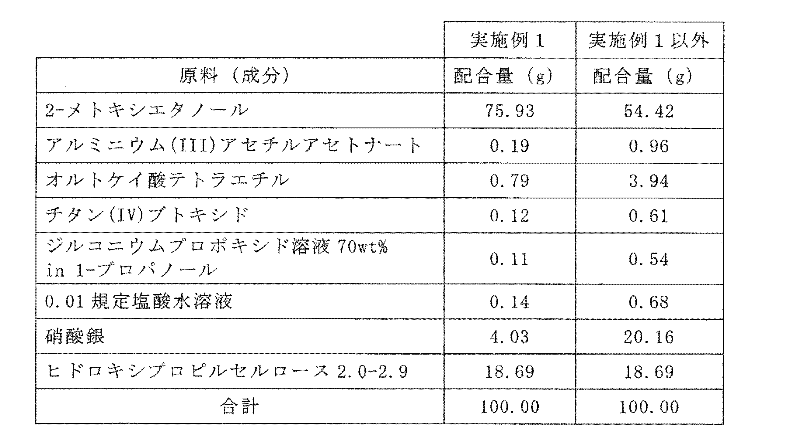
表1の「実施例1」に示す原料(成分)を、所定質量にて混合して原料組成物(ペースト)を調製した。なお、ペーストは、ガラスの前駆体として、Siアルコキシド(TEOS:オルトケイ酸テトラエチル)、Tiアルコキシド(TiBu:チタンブトキシド)、Zrアルコキシド(ZrPr:ジルコニアプロポキシド)を含む。0.01N-HCl(0.01規定塩酸水溶液)は、触媒である酸と加水分解用の水として機能し、HPC(ヒドロキシプロピルセルロース)は、粘度調整剤および安定化剤として機能する。
次に、上記セラミック素体41の両端部(両端面およびその近傍に位置する側面の一部)に、原料組成物を塗布し、空気雰囲気(常圧)下、150℃にて30分間乾燥させて、原料組成物に由来する塗膜を形成した。
表1の「実施例1」に示す原料(成分)を、所定質量にて混合して原料組成物(ペースト)を調製した。なお、ペーストは、ガラスの前駆体として、Siアルコキシド(TEOS:オルトケイ酸テトラエチル)、Tiアルコキシド(TiBu:チタンブトキシド)、Zrアルコキシド(ZrPr:ジルコニアプロポキシド)を含む。0.01N-HCl(0.01規定塩酸水溶液)は、触媒である酸と加水分解用の水として機能し、HPC(ヒドロキシプロピルセルロース)は、粘度調整剤および安定化剤として機能する。
次に、上記セラミック素体41の両端部(両端面およびその近傍に位置する側面の一部)に、原料組成物を塗布し、空気雰囲気(常圧)下、150℃にて30分間乾燥させて、原料組成物に由来する塗膜を形成した。
その後、塗膜付きのセラミック素体41を、空気雰囲気(常圧)下、635℃にて30分間加熱処理を行い、塗膜に由来する下地層46を形成した(図4(b)参照)。
3)金属層48の形成
得られた下地層46付きのセラミック素体41を用いて、電解めっきにより、下地層46上に金属層48としてNi金属層を形成した(図4(b)参照)。
得られた下地層46付きのセラミック素体41を用いて、電解めっきにより、下地層46上に金属層48としてNi金属層を形成した(図4(b)参照)。
これにより、セラミック素体41の表面に、下地層46とその上に形成された金属層48とから構成される外部電極49a、49bを備えた試料を得た。外部電極49a、49bは、セラミック素体41の両端部(両端面およびその近傍に位置する側面の一部)を覆うものとなった。
・評価
本実施例に従って得られた試料を下記のように評価した。
本実施例に従って得られた試料を下記のように評価した。
SEM装置を使用して、本実施例の試料(加熱処理の温度:635℃)の断面を観察した。得られたSEM像(図5)で確認したところ、下地層46の厚さは109nmであった。導電性ペーストとして市販の銀ペーストを使用して形成される下地層の厚さは約10μmであり得るのに対して、本実施例の試料における下地層46は、その約1/90程度まで薄膜化することができた。
TEM-EDX装置(FE-TEM/EDX(JEOL JEM-F200(日本電子株式会社製)/分析システム Noran system 7(サーモフィッシャーサイエンティフィック社製)))を使用して、本実施例の試料(加熱処理の温度:635℃)を加工して下地層46の厚さ方向断面を露出させ、露出断面を観察および分析した。得られたSTEM像を図5に、Si、AgおよびNiに関するTEM-EDX像を図6~8にそれぞれ示す。なお、図5~8中、下側がセラミック素体41の内部電極45a、45bであり、上側がNi金属層48である。
図6に示す下地層46のTEM-EDX像(Si)から理解されるように、下地層46中のガラス領域(Si)の面積は、セラミック素体41側(内部電極45a、45b側)から金属層48側に向かって少なくなっている。逆に、図7に示す下地層46のTEM-EDX像(Ag)から理解されるように、下地金属領域(Ag)の面積は、セラミック素体41側(内部電極45a、45b側)から金属層48側に向かって多くなっている。よって、下地層46の金属層48により近い部分における下地金属/ガラス比が、下地層46のセラミック素体41(内部電極45a、45b)により近い部分における下地金属/ガラス比より高くなっていることが分かった。
なお、内部電極45a、45bと下地金属領域はともにAgから形成されているが、ガラス(Si)のEDXからそれらの界面は明確に区別することができた。
なお、内部電極45a、45bと下地金属領域はともにAgから形成されているが、ガラス(Si)のEDXからそれらの界面は明確に区別することができた。
図8に示す下地層のTEM-EDX像(Ni)から、Ni金属層48が、下地層46の表面に形成され、さらに金属層48の一部が下地層46の内部を通って広がり、下地層46とセラミック素体41との界面まで到達したことが確認された。下地層46の内部に広がっているNi金属層は、下地層46の細孔が存在していた部分を埋めるように広がることから、Ni金属層48を形成する前は、下地層46には細孔があったことが分かる。また、Ni金属層48が、下地層46の表面(金属層との界面)から、下地層46とセラミック素体41との界面まで到達しているので、下地層46の細孔は、下地層46の表面からセラミック素体41との界面まで連通していたことも分かる。
Ni金属層48の一部が下地層46の細孔内部からセラミック素体41との界面まで到達していることにより、Ni金属層48と下地層46は強固に結合し、Ni金属層48は下地層46から容易に剥離しない(金属層48と下地層46の結合力が高い)といえる。
(実施例2~6、比較例1~2)
原料組成物を表1の「実施例1以外」に沿って調製したこと、加熱処理の温度を表2に示す温度としたこと以外は、実施例1と同様にして、セラミック素体41の表面に下地層46を形成して、試料を得た(実施例2~6、比較例1~2)。各処理温度で加熱処理して得られた下地層46の露出表面のSEM像を図9~図15に示す。
原料組成物を表1の「実施例1以外」に沿って調製したこと、加熱処理の温度を表2に示す温度としたこと以外は、実施例1と同様にして、セラミック素体41の表面に下地層46を形成して、試料を得た(実施例2~6、比較例1~2)。各処理温度で加熱処理して得られた下地層46の露出表面のSEM像を図9~図15に示す。
実施例2~6、比較例1~2に従って得られた試料について、下地層46の膜厚、電気抵抗を測定した。さらに、各試料の下地層46の表面に電解めっきでNi金属層48を形成し、電解めっきの成形性、金属層48の状態(金属層48の一部が下地層46の裏面まで到達しているか)、下地層46の空隙率について調べた。それらの結果を表2に記載した。表2中、「-」は「測定せず」を意味する。
試料の電気抵抗は、調整したペーストをそれぞれセラミック基板上にスピンコートなどで塗布、焼成し、デジタルマルチメーターを用いて端子間0.5mmで測定した。空隙が減ると、電気抵抗は小さくなった。
「電解めっきの形成」では、下地層46の表面にNi金属層48を電解めっきで形成できるかどうかを評価した。表中の「○」はめっき可能であったことを示している。なお、試料の電気抵抗が低くても、加熱温度が150℃では、粘度調整と安定性付与のため加えた樹脂が残ってしまっており、下地層46とNi金属層48との密着性が確保できないため、めっきの引張応力で剥離が生じた。表中の「×」は、抵抗が確保できていないので、めっきできなかったことを示している。
金属層48の状態(金属層48の一部が下地層の裏面まで到達しているか)については、実施例1と同様に、下地層46の表面にNi金属層48形成した後に加工して下地層46の厚さ方向断面を露出させ、露出断面のSTEM像およびTEM-EDX像を観察して特定した。
また、下地層46の表面にNi金属膜48を形成した後に、下地層46の空隙率を求めた。空隙率は、上述した方法により求めた。なお、EDX分析を行う元素は、酸素(O)、アルミニウム(Al)、ケイ素(Si)、チタン(Ti)、鉄(Fe)、ニッケル(Ni)、亜鉛(Zn)、ジルコニウム(Zr)、銀(Ag)およびスズ(Sn)とした。
下地層と金属層の密着性は、以下のように評価した。下地層46の表面にNi金属層48を形成した。その後、試験用基板の表面に対して、金属層48の表面を接着面として接着剤により接着した。次に、サンプルを試験用基板の表面と平行な方向に加圧し(つまり、剪断力を加え)、金属層48が下地層46から剥がれるときの加圧力(剪断力)を求めて、剥がれ強度(N)を確認した。剥がれ強度が5N以下をNG(×)、それ以上をG(○)として評価した。
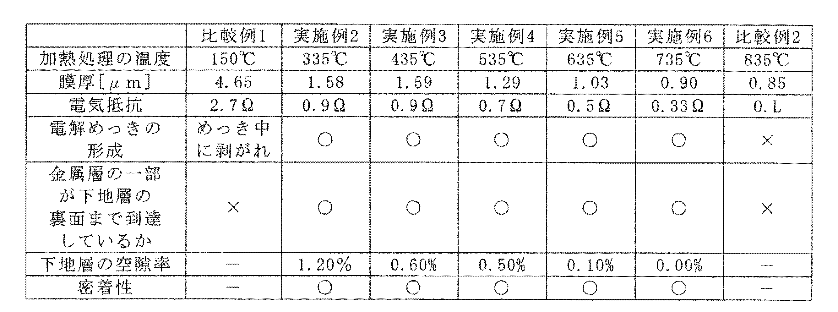
表2の結果を考察する。
実施例2~6では、加熱温度が適切であったので、金属層48の一部が下地層46の裏面まで到達していたため、下地層46と金属層48との密着性が良好であった。一方、比較例1~2は、加熱温度が適切ではなかったため、金属層48が下地層46の裏面まで到達せず、下地層46と金属層48との密着性が不十分であった。
実施例2~6では、加熱温度が適切であったので、金属層48の一部が下地層46の裏面まで到達していたため、下地層46と金属層48との密着性が良好であった。一方、比較例1~2は、加熱温度が適切ではなかったため、金属層48が下地層46の裏面まで到達せず、下地層46と金属層48との密着性が不十分であった。
(実施例7、比較例3)
実施例7では、実施例1で下地層46を焼付けした後のサンプルを用いて、図16に示した条件でNiめっきを行ってNiめっき膜(Ni金属層48)を形成した。そのときの積算電流とNi金属層48の膜厚との関係を評価した。比較例3は、一般的な銀ペースト(Ag粒子73wt%,ガラスフリット(ZnO-B2O3-SiO2)4wt%,エチルセルロース10wt%,ブチルカルビトールアセテートとエチルカルビトールとの1:1混合液13wt%)を用いて下地電極を形成したものについて、Niめっきを行った。図16から分かるように、同じ積算電流の場合であっても、実施例7はNiめっき膜(Ni金属層48)の膜厚が、比較例3のめっき膜の膜厚よりも大きくなることがわかった。このことから、実施例7は、下地金属/ガラス比が大きいことがわかった。
実施例7では、実施例1で下地層46を焼付けした後のサンプルを用いて、図16に示した条件でNiめっきを行ってNiめっき膜(Ni金属層48)を形成した。そのときの積算電流とNi金属層48の膜厚との関係を評価した。比較例3は、一般的な銀ペースト(Ag粒子73wt%,ガラスフリット(ZnO-B2O3-SiO2)4wt%,エチルセルロース10wt%,ブチルカルビトールアセテートとエチルカルビトールとの1:1混合液13wt%)を用いて下地電極を形成したものについて、Niめっきを行った。図16から分かるように、同じ積算電流の場合であっても、実施例7はNiめっき膜(Ni金属層48)の膜厚が、比較例3のめっき膜の膜厚よりも大きくなることがわかった。このことから、実施例7は、下地金属/ガラス比が大きいことがわかった。
本願は、2021年3月26日付けで日本国にて出願された特願2021-054076に基づく優先権を主張し、その記載内容の全てが、参照することにより本明細書に援用される。
1、41 セラミック素体
3、43 セラミック部
5a、5b、45a、45b 内部電極
6、46 下地層
8、48 金属層
9、9a、9b、49a、49b 外部電極
10 電子部品(積層セラミックコンデンサ)
11 下地金属領域
13 ガラス領域
40 電子部品(積層インダクタ)
44 コイル導体
3、43 セラミック部
5a、5b、45a、45b 内部電極
6、46 下地層
8、48 金属層
9、9a、9b、49a、49b 外部電極
10 電子部品(積層セラミックコンデンサ)
11 下地金属領域
13 ガラス領域
40 電子部品(積層インダクタ)
44 コイル導体
Claims (8)
- セラミック素体と、該セラミック素体の表面に設けられた外部電極とを備える電子部品であって、
該外部電極は、前記セラミック素体の表面に接触する下地層と、該下地層の表面上に形成された金属層とを含み、
前記下地層は、その表面から、前記セラミック素体との界面まで連通する細孔を有し、
前記金属層の一部は、前記細孔内を通って前記界面まで延在しており、
前記下地層内の空隙は1.5体積%以下である、電子部品。 - 前記下地層の厚さは0.1μm以上2μm以下である、請求項1に記載の電子部品。
- 前記下地層は、下地金属とガラスとを含み、
該下地層の前記金属層により近い部分における前記ガラスに対する前記下地金属の体積比は、前記下地層の前記セラミック素体により近い部分における前記ガラスに対する前記下地金属の体積比より高い、請求項1または2に記載の電子部品。 - 該下地層の前記金属層により近い部分における前記体積比が50%以上である、請求項3に記載の電子部品。
- 前記下地層は前記下地金属からなる下地金属領域と前記ガラスからなるガラス領域とを含み、
断面視において前記下地層の厚さ方向に沿って引いた直線上に、少なくとも2つの前記下地金属領域と少なくとも2つの前記ガラス領域が交互に配置されている、請求項3または4に記載の電子部品。 - 前記下地金属は銀であり、
前記ガラスはケイ素原子、チタン原子およびジルコニウム原子を含み、
前記金属層はニッケル、銅、スズからなる群から選択される1種以上を含む、請求項3~5のいずれか1項に記載の電子部品。 - セラミック素体と、該セラミック素体の表面に設けられた外部電極とを備える電子部品を製造する方法であって、
該外部電極は、前記セラミック素体の表面に接触する下地層と、該下地層の表面上に形成された金属層とを含み、前記下地層は下地金属とガラスとを含み、
前記方法は、
前記ガラスの原料となるガラス前駆体と、前記下地金属の原料となる金属塩と、増粘剤である有機高分子と、室温における蒸気圧が0.1kPa以上の溶媒とを含む原料組成物を調製し、当該原料組成物を前記セラミック素体の表面に塗布した後に加熱処理して下地層を形成する工程と、
前記下地層の表面に、電解めっきにより前記金属層を形成する工程とを含む、電子部品の製造方法。 - 前記下地層を形成する工程における加熱処理は、300℃以上835℃未満の温度で行う、請求項7に記載の製造方法。
Priority Applications (2)
| Application Number | Priority Date | Filing Date | Title |
|---|---|---|---|
| JP2023508810A JP7619438B2 (ja) | 2021-03-26 | 2022-02-21 | 電子部品およびその製造方法 |
| US18/362,108 US12476049B2 (en) | 2021-03-26 | 2023-07-31 | Electronic component and method for manufacturing the same |
Applications Claiming Priority (2)
| Application Number | Priority Date | Filing Date | Title |
|---|---|---|---|
| JP2021-054076 | 2021-03-26 | ||
| JP2021054076 | 2021-03-26 |
Related Child Applications (1)
| Application Number | Title | Priority Date | Filing Date |
|---|---|---|---|
| US18/362,108 Continuation US12476049B2 (en) | 2021-03-26 | 2023-07-31 | Electronic component and method for manufacturing the same |
Publications (1)
| Publication Number | Publication Date |
|---|---|
| WO2022202038A1 true WO2022202038A1 (ja) | 2022-09-29 |
Family
ID=83397041
Family Applications (1)
| Application Number | Title | Priority Date | Filing Date |
|---|---|---|---|
| PCT/JP2022/007002 Ceased WO2022202038A1 (ja) | 2021-03-26 | 2022-02-21 | 電子部品およびその製造方法 |
Country Status (3)
| Country | Link |
|---|---|
| US (1) | US12476049B2 (ja) |
| JP (1) | JP7619438B2 (ja) |
| WO (1) | WO2022202038A1 (ja) |
Cited By (6)
| Publication number | Priority date | Publication date | Assignee | Title |
|---|---|---|---|---|
| WO2024135396A1 (ja) * | 2022-12-20 | 2024-06-27 | 株式会社村田製作所 | 積層セラミック電子部品およびその製造方法 |
| WO2024135398A1 (ja) * | 2022-12-20 | 2024-06-27 | 株式会社村田製作所 | 導電材料、セラミック電子部品およびその製造方法 |
| WO2024135397A1 (ja) * | 2022-12-20 | 2024-06-27 | 株式会社村田製作所 | 積層セラミック電子部品、導電材料および積層セラミック電子部品の製造方法 |
| KR102810064B1 (ko) * | 2023-12-01 | 2025-05-23 | 주식회사 베이스 | 글라스 프릿 및 이를 포함하는 적층 세라믹 커패시터의 외부 전극용 도전성 페이스트 조성물 |
| WO2025258316A1 (ja) * | 2024-06-11 | 2025-12-18 | 株式会社村田製作所 | チップインダクタ及び実装構造 |
| WO2025258317A1 (ja) * | 2024-06-11 | 2025-12-18 | 株式会社村田製作所 | チップインダクタ |
Families Citing this family (2)
| Publication number | Priority date | Publication date | Assignee | Title |
|---|---|---|---|---|
| WO2020241739A1 (ja) * | 2019-05-29 | 2020-12-03 | 国立大学法人大阪大学 | 接合構造体の製造方法、及び接合構造体 |
| JP2024086583A (ja) * | 2022-12-16 | 2024-06-27 | サムソン エレクトロ-メカニックス カンパニーリミテッド. | 積層型キャパシタおよびその製造方法 |
Citations (5)
| Publication number | Priority date | Publication date | Assignee | Title |
|---|---|---|---|---|
| JPH06215981A (ja) * | 1993-01-16 | 1994-08-05 | Tdk Corp | セラミック電子部品 |
| JP2013106035A (ja) * | 2011-11-11 | 2013-05-30 | Samsung Electro-Mechanics Co Ltd | 積層セラミック電子部品 |
| WO2016186053A1 (ja) * | 2015-05-21 | 2016-11-24 | 株式会社村田製作所 | 電子部品 |
| JP2018032788A (ja) * | 2016-08-25 | 2018-03-01 | 太陽誘電株式会社 | 積層セラミックコンデンサおよびその製造方法 |
| JP2018157183A (ja) * | 2016-09-28 | 2018-10-04 | 株式会社村田製作所 | 電子部品 |
Family Cites Families (9)
| Publication number | Priority date | Publication date | Assignee | Title |
|---|---|---|---|---|
| JP2001244116A (ja) | 2000-02-29 | 2001-09-07 | Taiyo Yuden Co Ltd | 電子部品及びその製造方法 |
| JP2011014564A (ja) * | 2009-06-30 | 2011-01-20 | Murata Mfg Co Ltd | 積層型セラミック電子部品およびその製造方法 |
| JP2015035581A (ja) * | 2013-07-10 | 2015-02-19 | 株式会社村田製作所 | セラミック電子部品およびその製造方法 |
| US9859056B2 (en) * | 2014-09-30 | 2018-01-02 | Murata Manufacturing Co., Ltd. | Multilayer ceramic capacitor |
| JP6809865B2 (ja) * | 2016-10-17 | 2021-01-06 | 太陽誘電株式会社 | セラミック電子部品及びその製造方法 |
| JP7243487B2 (ja) * | 2019-06-27 | 2023-03-22 | 株式会社村田製作所 | 積層セラミックコンデンサの製造方法 |
| KR102880981B1 (ko) * | 2020-12-14 | 2025-11-04 | 삼성전기주식회사 | 적층형 전자 부품 |
| KR102900297B1 (ko) * | 2020-12-31 | 2025-12-12 | 삼성전기주식회사 | 적층 세라믹 전자부품 |
| JP7544627B2 (ja) * | 2021-03-08 | 2024-09-03 | Tdk株式会社 | セラミック電子部品 |
-
2022
- 2022-02-21 JP JP2023508810A patent/JP7619438B2/ja active Active
- 2022-02-21 WO PCT/JP2022/007002 patent/WO2022202038A1/ja not_active Ceased
-
2023
- 2023-07-31 US US18/362,108 patent/US12476049B2/en active Active
Patent Citations (5)
| Publication number | Priority date | Publication date | Assignee | Title |
|---|---|---|---|---|
| JPH06215981A (ja) * | 1993-01-16 | 1994-08-05 | Tdk Corp | セラミック電子部品 |
| JP2013106035A (ja) * | 2011-11-11 | 2013-05-30 | Samsung Electro-Mechanics Co Ltd | 積層セラミック電子部品 |
| WO2016186053A1 (ja) * | 2015-05-21 | 2016-11-24 | 株式会社村田製作所 | 電子部品 |
| JP2018032788A (ja) * | 2016-08-25 | 2018-03-01 | 太陽誘電株式会社 | 積層セラミックコンデンサおよびその製造方法 |
| JP2018157183A (ja) * | 2016-09-28 | 2018-10-04 | 株式会社村田製作所 | 電子部品 |
Cited By (6)
| Publication number | Priority date | Publication date | Assignee | Title |
|---|---|---|---|---|
| WO2024135396A1 (ja) * | 2022-12-20 | 2024-06-27 | 株式会社村田製作所 | 積層セラミック電子部品およびその製造方法 |
| WO2024135398A1 (ja) * | 2022-12-20 | 2024-06-27 | 株式会社村田製作所 | 導電材料、セラミック電子部品およびその製造方法 |
| WO2024135397A1 (ja) * | 2022-12-20 | 2024-06-27 | 株式会社村田製作所 | 積層セラミック電子部品、導電材料および積層セラミック電子部品の製造方法 |
| KR102810064B1 (ko) * | 2023-12-01 | 2025-05-23 | 주식회사 베이스 | 글라스 프릿 및 이를 포함하는 적층 세라믹 커패시터의 외부 전극용 도전성 페이스트 조성물 |
| WO2025258316A1 (ja) * | 2024-06-11 | 2025-12-18 | 株式会社村田製作所 | チップインダクタ及び実装構造 |
| WO2025258317A1 (ja) * | 2024-06-11 | 2025-12-18 | 株式会社村田製作所 | チップインダクタ |
Also Published As
| Publication number | Publication date |
|---|---|
| JPWO2022202038A1 (ja) | 2022-09-29 |
| US12476049B2 (en) | 2025-11-18 |
| US20230377800A1 (en) | 2023-11-23 |
| JP7619438B2 (ja) | 2025-01-22 |
Similar Documents
| Publication | Publication Date | Title |
|---|---|---|
| JP7619438B2 (ja) | 電子部品およびその製造方法 | |
| JP6610663B2 (ja) | 電子部品 | |
| US12308174B2 (en) | Electronic component | |
| US11887788B2 (en) | Electronic component | |
| US12497326B2 (en) | Surface-modified glass, electronic component, and method for forming silicate film | |
| US20240021346A1 (en) | Electronic component | |
| US20240021347A1 (en) | Electronic component | |
| TW201609379A (zh) | 陶瓷電子零件及其製造方法 | |
| US20240304363A1 (en) | Electronic component | |
| US20250266189A1 (en) | Protective glass film | |
| WO2017163931A1 (ja) | セラミック電子部品およびセラミック電子部品の製造方法 | |
| US20240221981A1 (en) | Electronic component and film forming method | |
| JP6369560B2 (ja) | セラミック配線基板およびセラミック配線基板の製造方法 | |
| KR102834756B1 (ko) | 세라믹 전자 부품 및 그 제조 방법 | |
| JP5104030B2 (ja) | 多層セラミック基板およびその製造方法 | |
| US20250118462A1 (en) | Electronic component | |
| JP3724021B2 (ja) | 導電性組成物およびそれを用いたセラミックコンデンサ | |
| WO2025169709A1 (ja) | 電子部品 | |
| WO2025249191A1 (ja) | 電子部品 | |
| JP2002128581A (ja) | 銅メタライズ組成物ならびにそれを用いたセラミック配線基板およびその製造方法 | |
| KR20250086724A (ko) | 적층 세라믹 전자부품, 도전 재료 및 적층 세라믹 전자부품의 제조 방법 | |
| KR20250109739A (ko) | 도전 재료, 세라믹 전자부품 및 그 제조 방법 | |
| JP2010225959A (ja) | 多層配線基板 | |
| JP2012077324A (ja) | Niめっき液 |
Legal Events
| Date | Code | Title | Description |
|---|---|---|---|
| 121 | Ep: the epo has been informed by wipo that ep was designated in this application |
Ref document number: 22774838 Country of ref document: EP Kind code of ref document: A1 |
|
| ENP | Entry into the national phase |
Ref document number: 2023508810 Country of ref document: JP Kind code of ref document: A |
|
| NENP | Non-entry into the national phase |
Ref country code: DE |
|
| 122 | Ep: pct application non-entry in european phase |
Ref document number: 22774838 Country of ref document: EP Kind code of ref document: A1 |