WO2022201681A1 - 半導体装置及び超音波センサ - Google Patents
半導体装置及び超音波センサ Download PDFInfo
- Publication number
- WO2022201681A1 WO2022201681A1 PCT/JP2021/046960 JP2021046960W WO2022201681A1 WO 2022201681 A1 WO2022201681 A1 WO 2022201681A1 JP 2021046960 W JP2021046960 W JP 2021046960W WO 2022201681 A1 WO2022201681 A1 WO 2022201681A1
- Authority
- WO
- WIPO (PCT)
- Prior art keywords
- switch
- piezoelectric element
- circuit
- signal
- braking
- Prior art date
- Legal status (The legal status is an assumption and is not a legal conclusion. Google has not performed a legal analysis and makes no representation as to the accuracy of the status listed.)
- Ceased
Links
Images






Classifications
-
- G—PHYSICS
- G01—MEASURING; TESTING
- G01S—RADIO DIRECTION-FINDING; RADIO NAVIGATION; DETERMINING DISTANCE OR VELOCITY BY USE OF RADIO WAVES; LOCATING OR PRESENCE-DETECTING BY USE OF THE REFLECTION OR RERADIATION OF RADIO WAVES; ANALOGOUS ARRANGEMENTS USING OTHER WAVES
- G01S15/00—Systems using the reflection or reradiation of acoustic waves, e.g. sonar systems
- G01S15/02—Systems using the reflection or reradiation of acoustic waves, e.g. sonar systems using reflection of acoustic waves
- G01S15/06—Systems determining the position data of a target
- G01S15/08—Systems for measuring distance only
- G01S15/10—Systems for measuring distance only using transmission of interrupted, pulse-modulated waves
-
- B—PERFORMING OPERATIONS; TRANSPORTING
- B06—GENERATING OR TRANSMITTING MECHANICAL VIBRATIONS IN GENERAL
- B06B—METHODS OR APPARATUS FOR GENERATING OR TRANSMITTING MECHANICAL VIBRATIONS OF INFRASONIC, SONIC, OR ULTRASONIC FREQUENCY, e.g. FOR PERFORMING MECHANICAL WORK IN GENERAL
- B06B1/00—Methods or apparatus for generating mechanical vibrations of infrasonic, sonic, or ultrasonic frequency
- B06B1/02—Methods or apparatus for generating mechanical vibrations of infrasonic, sonic, or ultrasonic frequency making use of electrical energy
- B06B1/06—Methods or apparatus for generating mechanical vibrations of infrasonic, sonic, or ultrasonic frequency making use of electrical energy operating with piezoelectric effect or with electrostriction
- B06B1/0644—Methods or apparatus for generating mechanical vibrations of infrasonic, sonic, or ultrasonic frequency making use of electrical energy operating with piezoelectric effect or with electrostriction using a single piezoelectric element
- B06B1/0662—Methods or apparatus for generating mechanical vibrations of infrasonic, sonic, or ultrasonic frequency making use of electrical energy operating with piezoelectric effect or with electrostriction using a single piezoelectric element with an electrode on the sensitive surface
- B06B1/0681—Methods or apparatus for generating mechanical vibrations of infrasonic, sonic, or ultrasonic frequency making use of electrical energy operating with piezoelectric effect or with electrostriction using a single piezoelectric element with an electrode on the sensitive surface and a damping structure
-
- G—PHYSICS
- G01—MEASURING; TESTING
- G01S—RADIO DIRECTION-FINDING; RADIO NAVIGATION; DETERMINING DISTANCE OR VELOCITY BY USE OF RADIO WAVES; LOCATING OR PRESENCE-DETECTING BY USE OF THE REFLECTION OR RERADIATION OF RADIO WAVES; ANALOGOUS ARRANGEMENTS USING OTHER WAVES
- G01S15/00—Systems using the reflection or reradiation of acoustic waves, e.g. sonar systems
- G01S15/02—Systems using the reflection or reradiation of acoustic waves, e.g. sonar systems using reflection of acoustic waves
- G01S15/04—Systems determining presence of a target
-
- G—PHYSICS
- G01—MEASURING; TESTING
- G01S—RADIO DIRECTION-FINDING; RADIO NAVIGATION; DETERMINING DISTANCE OR VELOCITY BY USE OF RADIO WAVES; LOCATING OR PRESENCE-DETECTING BY USE OF THE REFLECTION OR RERADIATION OF RADIO WAVES; ANALOGOUS ARRANGEMENTS USING OTHER WAVES
- G01S7/00—Details of systems according to groups G01S13/00, G01S15/00, G01S17/00
- G01S7/52—Details of systems according to groups G01S13/00, G01S15/00, G01S17/00 of systems according to group G01S15/00
- G01S7/523—Details of pulse systems
-
- H—ELECTRICITY
- H10—SEMICONDUCTOR DEVICES; ELECTRIC SOLID-STATE DEVICES NOT OTHERWISE PROVIDED FOR
- H10N—ELECTRIC SOLID-STATE DEVICES NOT OTHERWISE PROVIDED FOR
- H10N30/00—Piezoelectric or electrostrictive devices
-
- G—PHYSICS
- G01—MEASURING; TESTING
- G01S—RADIO DIRECTION-FINDING; RADIO NAVIGATION; DETERMINING DISTANCE OR VELOCITY BY USE OF RADIO WAVES; LOCATING OR PRESENCE-DETECTING BY USE OF THE REFLECTION OR RERADIATION OF RADIO WAVES; ANALOGOUS ARRANGEMENTS USING OTHER WAVES
- G01S15/00—Systems using the reflection or reradiation of acoustic waves, e.g. sonar systems
- G01S15/88—Sonar systems specially adapted for specific applications
- G01S15/93—Sonar systems specially adapted for specific applications for anti-collision purposes
- G01S15/931—Sonar systems specially adapted for specific applications for anti-collision purposes of land vehicles
-
- G—PHYSICS
- G01—MEASURING; TESTING
- G01S—RADIO DIRECTION-FINDING; RADIO NAVIGATION; DETERMINING DISTANCE OR VELOCITY BY USE OF RADIO WAVES; LOCATING OR PRESENCE-DETECTING BY USE OF THE REFLECTION OR RERADIATION OF RADIO WAVES; ANALOGOUS ARRANGEMENTS USING OTHER WAVES
- G01S7/00—Details of systems according to groups G01S13/00, G01S15/00, G01S17/00
- G01S7/52—Details of systems according to groups G01S13/00, G01S15/00, G01S17/00 of systems according to group G01S15/00
- G01S7/523—Details of pulse systems
- G01S7/524—Transmitters
Definitions
- the present disclosure relates to semiconductor devices and ultrasonic sensors.
- Ultrasonic sensors equipped with piezoelectric elements are used for various purposes.
- An ultrasonic sensor transmits a transmission wave signal by driving a piezoelectric element and receives a reflected wave signal to detect the distance or proximity of an object (see, for example, Patent Document 1).
- the piezoelectric element Even after the supply of the drive signal for transmitting the transmission wave signal to the piezoelectric element is stopped, the piezoelectric element continues to vibrate for a while based on the mechanical energy it has accumulated. Vibration of the piezoelectric element after the supply of the drive signal is stopped is called reverberation. If the reverberation continues for a long time (reverberation time), it becomes difficult to detect objects at close range. Therefore, the development of technology that can effectively reduce the reverberation time is expected.
- An object of the present disclosure is to provide a semiconductor device and an ultrasonic sensor that contribute to reducing reverberation time.
- a semiconductor device can supply a drive signal in an ultrasonic band to a piezoelectric element, and can supply a damping signal having a phase different from the phase of the drive signal to the piezoelectric element after the supply of the drive signal is stopped. and a control circuit configured to be able to control the drive circuit, the drive circuit connecting a first line and a second line to which a potential higher than that of the first line is applied.
- the full bridge circuit includes a series circuit of a first switch provided on the second line side and a second switch provided on the first line side, and a third switch provided on the second line side. and a fourth switch provided on the first line side, a connection node between the first switch and the second switch and a connection node between the third switch and the fourth switch and a first end and a second end of the piezoelectric element, respectively, and the control circuit supplies the braking signal to the piezoelectric element after stopping the supply of the drive signal to the piezoelectric element.
- the drive circuit is configured to be able to perform a braking operation before the braking operation, wherein the first switch and the third switch are turned off and the second switch and the fourth switch are turned on in the braking operation, or , the first switch and the third switch are turned on and the second switch and the fourth switch are turned off.
- FIG. 1 is an overall configuration diagram of an ultrasonic sensor according to an embodiment of the present disclosure.
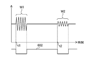
- FIG. 2 is a diagram illustrating the relationship between an output wave signal and a reflected wave signal in an ultrasonic sensor, according to an embodiment of the present disclosure;
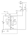
- FIG. 3 is a diagram showing the internal configuration of a semiconductor device that constitutes an ultrasonic sensor, according to an embodiment of the present disclosure.
- FIG. 4 is a diagram illustrating several possible states of a drive circuit in accordance with an embodiment of the present disclosure.
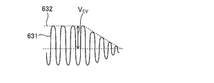
- FIG. 5 is a diagram illustrating the relationship between an amplified voltage signal based on a received signal and an envelope signal, according to an embodiment of the present disclosure.
- FIG. 6 is a diagram showing an internal configuration example of a damping circuit according to the embodiment of the present disclosure.
- FIG. 1 is an overall configuration diagram of an ultrasonic sensor according to an embodiment of the present disclosure.
- FIG. 2 is a diagram illustrating the relationship between an output wave signal and a reflected wave signal in an ultras
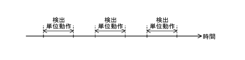
- FIG. 7 is a diagram illustrating how the semiconductor device repeatedly performs the detection unit operation according to the embodiment of the present disclosure.
- FIG. 8 is a diagram illustrating a configuration of a period during which detection unit operations are performed, according to an embodiment of the present disclosure.
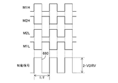
- FIG. 9 is a diagram showing the state of each switch and the waveform of the drive signal during the transmission period, according to the embodiment of the present disclosure.
- FIG. 10 is a diagram illustrating the state of each switch and the waveform of the braking signal during the first braking period, according to an embodiment of the present disclosure.
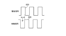
- FIG. 11 is a diagram illustrating the phase relationship between a drive signal and a brake signal, according to an embodiment of the present disclosure.
- FIG. 12 is a timing chart of a detection unit operation according to Example 1 belonging to the embodiment of the present disclosure.
- FIG. 13 is a timing chart of a detection unit operation according to a comparative example.
- FIG. 14 is a diagram showing a drive circuit and its peripheral circuits according to a second example belonging to an embodiment of the present disclosure.
- FIG. 15 is a timing chart of the detection unit operation according to the second example belonging to the embodiment of the present disclosure.
- FIG. 16 is a modified timing chart of the detection unit operation according to the second example belonging to the embodiment of the present disclosure.
- FIG. 17 is a timing chart of the detection unit operation according to the third example belonging to the embodiment of the present disclosure.
- FIG. 18 is a diagram showing a drive circuit and its peripheral circuits according to a fourth example belonging to an embodiment of the present disclosure.
- FIG. 19 is a timing chart of the detection unit operation according to the fourth example belonging to the embodiment of the present disclosure.
- FIG. 20 is a modified timing chart of the detection unit operation according to the fourth example belonging to the embodiment of the present disclosure.
- FIG. 21 is a schematic top view of a vehicle equipped with multiple ultrasonic sensors according to an embodiment of the present disclosure;
- Lines refer to wires through which electrical signals are propagated or applied.
- the ground refers to a reference conductive portion having a potential of 0 V (zero volt) as a reference, or refers to a potential of 0 V itself.
- the reference conductive portion is made of a conductor such as metal.
- a potential of 0 V is sometimes referred to as a ground potential.
- voltages shown without specific reference represent potentials with respect to ground.
- the ON state refers to the state in which there is conduction between the drain and source of the transistor
- the OFF state refers to the state in which there is conduction between the drain and source of the transistor. It refers to the state in which the current between the two is non-conducting (blocking state).
- MOSFETs are understood to be enhancement mode MOSFETs unless otherwise stated.
- MOSFET is an abbreviation for "metal-oxide-semiconductor field-effect transistor".
- An arbitrary switch can be composed of one or more FETs (Field Effect Transistors), and when a certain switch is in an ON state, the two ends of the switch are conductive, and when a certain switch is in an OFF state, the switch is closed. Both ends become non-conducting.
- FETs Field Effect Transistors
- the on state and off state of any transistor or switch may be simply expressed as on and off. Connections between a plurality of parts forming a circuit, such as arbitrary circuit elements, wirings (lines), nodes, etc., may be understood to refer to electrical connections unless otherwise specified.
- FIG. 1 shows the overall configuration of an ultrasonic sensor 1 according to an embodiment of the present disclosure.
- FIG. 1 also shows an upper block 2 connected to the ultrasonic sensor 1 and an object to be detected OBJ physically separated from the ultrasonic sensor 1 .
- the ultrasonic sensor 1 includes a semiconductor device 10 which is a semiconductor integrated circuit for ultrasonic sensors, a piezoelectric element 20, and capacitors 31 and 32. As shown in FIG. FIG. 1 shows only part of the internal configuration of the semiconductor device 10. As shown in FIG.
- the ultrasonic sensor 1 transmits an output wave signal W1 in the ultrasonic band toward the external space of the ultrasonic sensor 1 (in a direction away from the ultrasonic sensor 1).
- a reflected wave signal W2 is generated by reflecting the output wave signal W1 from the detection object OBJ.
- the reflected wave signal W2 is received by the ultrasonic sensor 1 .
- the ultrasonic sensor 1 performs detection of the distance to the object to be detected OBJ, detection of proximity of the object to be detected OBJ, and the like based on the received signal of the reflected wave signal W2.
- the ultrasonic band refers to a frequency band that is higher than the band of sound waves audible to human ears and inaudible to human ears, and generally refers to a band of 20 kHz or higher.
- output wave signal W1 has a frequency in the range of 30 kHz to 80 kHz. Both the output wave signal W1 and the reflected wave signal W2 belong to the ultrasonic signal.
- the piezoelectric element 20 has a first end and a second end.
- the piezoelectric element 20 produces mechanical displacement (vibration) in response to a voltage signal applied between the first and second ends, and the mechanical displacement generates an output wave signal W1. Therefore, the piezoelectric element 20 functions as a transmitter for the output wave signal W1.
- the piezoelectric element 20 has a characteristic of generating an electromotive force between the first end and the second end in response to mechanical displacement (vibration) applied to itself, and also functions as a receiver for the reflected wave signal W2.
- the semiconductor device 10 uses the piezoelectric element 20 to transmit the output wave signal W1 and receive the reflected wave signal W2.
- a combination of the transmission operation of the output wave signal W1 and the reception operation of the reflected wave signal W2 may be referred to as a transmission/reception operation.
- a semiconductor device 10 includes a transmission circuit 11 , a reception circuit 12 and a control circuit 13 .
- the semiconductor device 10 is an electronic component formed by enclosing a semiconductor integrated circuit in a housing (package) made of resin, and each circuit constituting the semiconductor device 10 is integrated with a semiconductor.
- a housing of the electronic component as the semiconductor device 10 is provided with a plurality of external terminals exposed from the housing to the outside of the semiconductor device 10 .
- Output terminals DRV1 and DRV2 and input terminals IN1 and IN2 are shown in FIG. 1 as part of the plurality of external terminals provided in the semiconductor device 10 .
- the output terminal DRV1 is connected to the first end of the piezoelectric element 20 and the output terminal DRV2 is connected to the second end of the piezoelectric element 20 .
- the input terminal IN1 is connected to the first end of the piezoelectric element 20 via the capacitor 31
- the input terminal IN2 is connected to the second end of the piezoelectric element 20 via the capacitor 32.
- the capacitors 31 and 32 may be built in the semiconductor device 10 .
- the transmission circuit 11 transmits the output wave signal W1 using the piezoelectric element 20 externally connected between the output terminals DRV1 and DRV2.
- the receiving circuit 12 receives an input wave signal in an ultrasonic band using a piezoelectric element 20 externally connected between input terminals IN1 and IN2.
- the main input wave signal to be received is the reflected wave signal W2 based on the output wave signal W1.
- the common piezoelectric element 20 is externally connected between the output terminals DRV1 and DRV2 and between the input terminals IN1 and IN2, and the common piezoelectric element 20 serves as a transmitter/receiver. It is shared by the receiving circuit 12 .
- another piezoelectric element different from the piezoelectric element 20 may be externally connected between the input terminals IN1 and IN2 (in this case, the other piezoelectric element may also be an ultrasonic sensor). 1 component).
- the common piezoelectric element 20 is shared by the transmission circuit 11 and the reception circuit 12, the output terminal DRV1 and the input terminal IN1 are realized by one first input/output terminal, and the output terminal DRV2 and the input terminal IN2 are realized.
- the receiving circuit 12 receives an input wave signal in the ultrasonic band using the piezoelectric element 20 or other piezoelectric elements, and performs predetermined signal processing for reception on the received signal.
- the control circuit 13 controls the transmission circuit 11 and the reception circuit 12.
- the control circuit 13 controls the transmission circuit 11 to transmit the output wave signal W1 from the piezoelectric element 20 using the transmission circuit 11 . Further, the control circuit 13 detects the distance of the object to be detected OBJ and detects the approach of the object to be detected OBJ based on the signal received by the receiving circuit 12 (the input wave signal received by the receiving circuit 12).
- FIG. 2 is a diagram showing transmission and reception operations by the ultrasonic sensor 1.
- the control circuit 13 can perform distance detection processing and approach detection processing. In the distance detection process, the control circuit 13 determines the length of time from transmitting the output wave signal W1 at time t1 to receiving the reflected wave signal W2 at time t2 (that is, the length between times t1 and t2). ), the distance between the ultrasonic sensor 1 and the detection object OBJ is calculated.
- Time t1 represents the transmission start time of the output wave signal W1 using the transmission circuit 11 and the piezoelectric element 20
- time t2 represents the reception start time of the reflected wave signal W2 using the reception circuit 12 and the piezoelectric element 20.
- the control circuit 13 performs approach detection of the object to be detected OBJ based on whether or not the reflected wave signal W2 is received. More specifically, for example, in the approach detection process, when the control circuit 13 receives the reflected wave signal W2 within a predetermined time after transmitting the output wave signal W1 at time t1, the ultrasonic sensor 1 (for example, the vehicle on which the ultrasonic sensor 1 is mounted) is determined that the detection object OBJ is approaching. It is determined that the detection object OBJ is not approaching the vehicle on which 1 is mounted.
- the ultrasonic sensor 1 for example, the vehicle on which the ultrasonic sensor 1 is mounted
- the control circuit 13 is connected to the upper block 2 shown in FIG. 1 in a form capable of two-way communication.
- the upper block 2 can give various instructions to the semiconductor device 10 by transmitting predetermined commands to the semiconductor device 10, and the semiconductor device 10 performs various operations and processes according to the commands from the upper block 2. . Results of distance detection processing and approach detection processing are transmitted from the semiconductor device 10 to the upper block 2 .
- the upper block 2 consists of a microcomputer or the like. When the ultrasonic sensor 1 and the upper block 2 are mounted on a vehicle such as an automobile, the upper block 2 may be an ECU (Electronic Control Unit).
- the upper block 2 may determine whether or not the detection object OBJ is approaching (with respect to the vehicle). In this case, for example, a signal such as the signal 602 in FIG. should be sent to
- the semiconductor device 10 includes a drive circuit 111 , a gate driver 112 , a receiver circuit 120 and a control circuit 130 .
- the driving circuit 111 and the gate driver 112 constitute the transmission circuit 11 in FIG.
- the receiving circuit 120 corresponds to the receiving circuit 12 in FIG. 1 and has the functions of the receiving circuit 12 described above.
- the control circuit 130 corresponds to the control circuit 13 in FIG. 1 and has the functions of the control circuit 13 described above.
- the semiconductor device 10 further includes a damping circuit 140 , a switch circuit 150 and an internal power supply circuit 160 .
- the drive circuit 111 includes transistors M1H, M1L, M2H and M2L as four switching elements (switches).
- Transistors M1H and M2H are P-channel MOSFETs, and transistors M1L and M2L are N-channel MOSFETs.
- the transistors M1H and M1L are connected in series to form a first half bridge circuit (first series circuit), and the transistors M2H and M2L are connected in series to form a second half bridge circuit (second series circuit).
- a full bridge circuit (H bridge circuit) is configured by the first and second half bridge circuits.
- Each source of transistors M1H and M2H is connected to line LN2.
- a driving power supply voltage VDRV having a predetermined positive DC voltage value is applied to line LN2.
- the drains of transistors M1H and M1L are commonly connected to line LN10 and connected to output terminal DRV1 through line LN10.
- the drains of transistors M2H and M2L are commonly connected to line LN20 and connected to output terminal DRV2 through line LN20.
- Each source of transistors M1L and M2L is connected to line LN1.
- Ground potential is applied to line LN1.
- the output terminal DRV1 and the input terminal IN1 are connected to the first end of the piezoelectric element 20 outside the semiconductor device 10, and the output terminal DRV2 and the input terminal IN2 are connected to the second end of the piezoelectric element 20 outside the semiconductor device 10.
- the input terminals IN1 and IN2 are connected to the first and second ends of the piezoelectric element 20 via capacitors 31 and 32).
- a modification in which the transistors M1H and M2H are configured with N-channel MOSFETs is also possible (in this case, a circuit for generating a voltage higher than the drive power supply voltage VDRV is added).
- the gate driver 112 is driven using the drive power supply voltage VDRV applied to the line LN2 as the positive power supply voltage and the ground voltage (0 V) applied to the line LN1 as the negative power supply voltage.
- the gate driver 112 individually controls the on/off states of the transistors M1H, M1L, M2H and M2L by controlling the gate potentials of the transistors M1H, M1L, M2H and M2L according to the control signal CNT1 supplied from the control circuit 130. Control.
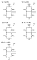
- the state of drive circuit 111 can be set to any of states 611-615 in FIG. It should be noted that the drive circuit 111 may assume a state different from any of the states 611-615.
- a state 611 is the first application state. In the first application state, transistors M1H and M2L are on and transistors M2H and M1L are off.
- State 612 is the second application state. In the second application state, transistors M1L and M2H are on and transistors M1H and M2L are off.
- State 613 is the all off state. In the all-off state, transistors M1H, M1L, M2H and M2L are all off.
- State 614 is the first braking state. In the first braking state, transistors M1L and M2L are on and transistors M1H and M2H are off.
- State 615 is the second brake state. In the second braking state, transistors M1L and M2L are off and transistors M1H and M2H are on.
- the receiving circuit 120 is connected to the input terminals IN1 and IN2 and receives a voltage signal applied between the input terminals IN1 and IN2. Therefore, when the reflected wave signal W2 is received by the piezoelectric element 20, a voltage signal generated between the first end and the second end of the piezoelectric element 20 based on the reflected wave signal W2 is supplied to the receiving circuit 120 through the input terminals IN1 and IN2. is entered.
- the receiving circuit 120 generates a detection signal based on the voltage signal between the input terminals IN1 and IN2 by performing predetermined signal processing for reception on the voltage signal between the input terminals IN1 and IN2.
- Signal processing for reception includes DC removal processing for removing a DC component from the voltage signal between the input terminals IN1 and IN2, amplification processing for amplifying the voltage signal after DC removal processing, and voltage signal after amplification processing (hereinafter referred to as amplification processing).
- amplification processing for amplifying the voltage signal after DC removal processing
- voltage signal after amplification processing (referred to as a voltage signal) includes envelope detection processing for detecting the envelope of the signal.
- a detected signal generated in the received signal 120 includes an envelope signal.
- capacitors 31 and 32 are provided between the input terminals IN1 and IN2 and the piezoelectric element 20 as shown in FIG. 3, the DC removal process can be omitted in the reception signal processing stage. In FIG.
- a solid-line waveform 631 is the waveform of the amplified voltage signal
- a dashed-line waveform 632 is the waveform of the envelope signal.
- the envelope signal is a voltage signal whose voltage value is the magnitude of the amplitude of the amplified voltage signal. Therefore, the envelope signal has a voltage value (hereinafter referred to as voltage value VEV ) that is proportional to the amplitude of the received signal of receiver circuit 120 (ie, the voltage signal across input terminals IN1 and IN2).
- the control circuit 130 performs the above-described distance detection processing and approach detection processing based on the detection signal generated by the reception circuit 120, and also controls the operation of each part in the semiconductor device 10 in an integrated manner. In this control, the control circuit 130 generates and outputs control signals CNT1, CNT2 and CNT ADJ .
- the control circuit 130 also includes a storage circuit 131 .
- the memory circuit 131 is provided with a nonvolatile memory and a volatile memory.
- the nonvolatile memory in the storage circuit 131 includes a memory in which data can be written only once (One Time Programmable ROM) or a memory in which data can be rewritten.
- Volatile memory in storage circuit 131 includes registers.
- Damping circuit 140 comprises resistive component 141 , inductive component 142 and bias supply circuit 143 .
- the resistance component 141 and the induction component 142 are elements used to reduce reverberation of the piezoelectric element 20 and function as loads of the piezoelectric element 20 . Therefore, the resistive component 141 and the inductive component 142 are hereinafter referred to as a resistive load 141 and an inductive load 142, respectively.
- the resistive load 141 and the inductive load 142 are connected in parallel with each other, and the parallel circuit of the resistive load 141 and the inductive load 142 is connected between the lines LN12 and LN22.
- a bias supply circuit 143 supplies a predetermined DC bias voltage (for example, 2V) to the line LN22.
- the resistive load 141 is formed so that the resistance value of the resistive load 141 is variable, and the inductive load 142 is formed so that the inductance value of the inductive load 142 is variable.
- the resistance value of the resistive load 141 and the inductance value of the inductive load 142 are variably set according to the control signal CNT ADJ from the control circuit 130 .
- the switch circuit 150 includes switches 151 and 152 .
- Each switch in the switch circuit 150 can be composed of one or more MOSFETs.
- Each switch in switch circuit 150 may be a bus switch capable of propagating analog signals.
- a first end of switch 151 is connected to line LN10 and a second end of switch 151 is connected to line LN12.
- a first end of switch 152 is connected to line LN20 and a second end of switch 152 is connected to line LN22.
- the switches 151 and 152 are controlled to be on or off based on the control signal CNT2 supplied from the control circuit .
- the control signal CNT2 is a binary signal having a value of "0" or "1". When the control signal CNT2 has a value of "1", the switches 151 and 152 are both turned on, and when the control signal CNT2 has a value of "0", both the switches 151 and 152 are turned off.
- the internal power supply circuit 160 generates a plurality of power supply voltages including the drive power supply voltage VDRV and the internal power supply voltage VDD based on the power supply voltage VCC supplied to the semiconductor device 10 from an external power supply (not shown). Each circuit in the semiconductor device 10 is driven based on any power supply voltage generated by the internal power supply circuit 160 .
- control circuit 130 and damping circuit 140 may be driven based on internal power supply voltage VDD.
- both the driving power supply voltage VDRV and the internal power supply voltage VDD have positive DC voltage values, but the internal power supply voltage VDD is lower than the driving power supply voltage VDRV.
- the drive power supply voltage VDRV is 36V or 72V
- the internal power supply voltage VDD is 3V or 5V.
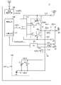
- FIG. 6 shows a specific configuration example of the damping circuit 140.
- the inductive load 142 is formed with a pseudo inductor so that the inductance value of the inductive load 142 can be arbitrarily changed within the semiconductor device 10 .
- the inductive load 142 is formed by a GIC (Generalized Impedance Converter) circuit.
- the inductive load 142 in FIG. 6 includes operational amplifiers 142a and 142b, fixed resistors 142c and 142e, variable resistors 142d and 142g, and a capacitor 142f. Fixed resistors 142c and 142e each have a fixed resistance value.
- the resistance values of the variable resistors 142d and 142g can be changed independently according to the control signal CNT ADJ from the control circuit 130, like the resistance value of the resistance load 141.
- the change in the resistance values of the variable resistors 142d and 142g changes the inductance value of the inductive load 142 connected between the lines LN12 and LN22.
- a first end of the fixed resistor 142c is commonly connected to the line LN12 and the non-inverting input terminal of the operational amplifier 142a.
- the second end of the resistor 142c is commonly connected to the first end of the variable resistor 142d and the output terminal of the operational amplifier 142b.
- the second end of the variable resistor 142d is commonly connected to the inverting input terminals of the operational amplifiers 142a and 142b and the first end of the fixed resistor 142e.
- the second end of the fixed resistor 142e is commonly connected to the output terminal of the operational amplifier 142a and the first end of the capacitor 142f.
- the second end of capacitor 142f is commonly connected to the first end of variable resistor 142g and the non-inverting input terminal of operational amplifier 142b.
- a second end of variable resistor 142g is connected to line LN22.
- the power supply voltages of the operational amplifiers 142a and 142b are determined so that the GIC circuit functions as an inductive load for the piezoelectric element 20 while the switches 151 and 152 are on.
- each of the switches 151 and 152 can be configured with an N-channel MOSFET.
- the MOSFET as switch 151 has its drain connected to line LN10 while its source is connected to line LN12
- the MOSFET as switch 152 has its drain connected to line LN20 while its source is connected to line LN22. Connected.
- the switches 151 and 152 are turned on or off.
- the configuration of the switches 151 and 152 is not limited to that shown in FIG. 6, and may be arbitrary.
- one or more detection unit operations can be performed under the control of the control circuit 130 in response to commands from the upper block 2.
- FIG. A distance detection process and an approach detection process are performed in each detection unit operation.
- FIG. 7 shows how a plurality of detection unit operations are successively and repeatedly executed.
- a period during which each detection unit operation is performed is called a detection unit period.
- each detection unit period is roughly divided into a transmission period, a braking period, a first braking period, a second braking period and a receiving period.
- a transmission period, a braking period, a first braking period, a second braking period, and a receiving period come in this order.
- the first damping period can also be called a damping pulse period
- the second damping period can also be called a damping period.
- the transmission period is the period during which the output wave signal W1 is transmitted.
- FIG. 9 shows the state of each switch in the drive circuit 111 during the transmission period and the waveform 650 of the drive signal supplied from the drive circuit 111 to the piezoelectric element 20 during the transmission period.
- the drive signal corresponds to a voltage signal applied between the output terminals DRV1 and DRV2 during the transmission period, and is assumed here to be a voltage signal having the potential of the output terminal DRV1 as viewed from the potential of the output terminal DRV2. Therefore, during the transmission period, the drive signal becomes a rectangular wave signal having a frequency f, and the voltage difference between the minimum and maximum values of the drive signal is twice the drive power supply voltage VDRV.
- the piezoelectric element 20 After the drive signal is supplied to the piezoelectric element 20 and then the supply of the drive signal is stopped, the piezoelectric element 20 continues to vibrate for a while based on the mechanical energy accumulated during the transmission period. Vibration of the piezoelectric element 20 after the supply of the drive signal is stopped is called reverberation. The duration of reverberation is called reverberation time. If the reverberation time is long, it becomes difficult to detect objects at close range. After the supply of the drive signal to the piezoelectric element 20 is stopped, the reverberation time can be reduced by supplying the piezoelectric element 20 with a signal having a phase opposite to that of the drive signal.
- a signal having a phase different from that of the driving signal is supplied from the driving circuit 111 to the piezoelectric element 20 as a braking signal, thereby reducing the reverberation time.
- the first braking period corresponds to the period during which the braking signal is supplied to the piezoelectric element 20 .
- FIG. 10 shows the state of each switch in the drive circuit 111 during the first braking period and the waveform 660 of the braking signal supplied from the drive circuit 111 to the piezoelectric element 20 during the first braking period.
- the state of the drive circuit 111 is alternately and periodically switched between the first applied state and the second applied state during the first braking period.
- the braking signal corresponds to the voltage signal applied between the output terminals DRV1 and DRV2 during the first braking period, and is assumed here to be the voltage signal having the potential of the output terminal DRV1 relative to the potential of the output terminal DRV2.
- the braking signal becomes a rectangular wave signal with frequency f, and the voltage difference between the minimum and maximum values of the braking signal is twice the driving power supply voltage VDRV.
- the frequency f of the braking signal is the same as the frequency f of the driving signal.
- Waveforms 650 and 660 of the driving signal and the braking signal are shown in FIG. Although the driving signal and the braking signal are not supplied to the piezoelectric element 20 at the same time, the waveforms 650 and 660 of the driving signal and the braking signal are shown side by side in FIG. 11 for convenience in order to show their phase relationship. ing.
- the phase of the braking signal relative to the phase of the driving signal is referenced by the symbol " ⁇ ".
- ⁇ the amount of phase delay of the braking signal with respect to the driving signal
- the phase ⁇ should have a value (angle) of 180° or close to it.
- Each detection unit operation is performed in a state in which the phase ⁇ , the resistance value of the resistive load 141 and the inductance value of the inductive load 142 are appropriately set based on the stored data in the storage circuit 131 and the like.
- the braking signal is sometimes called a damping pulse signal.
- the damping pulse signal is effective for reducing reverberation in a region where the reverberation amplitude (amplitude of the piezoelectric element 20 due to reverberation) is high. can be a factor.
- the mechanical energy is absorbed by the piezoelectric element 20 to reduce the reverberation.
- the inventors developed the following reverberation reduction operation.
- the driving circuit 111 supplies the braking signal to the piezoelectric element 20 , and after stopping the supplying of the braking signal, the damping circuit 140 is connected to the piezoelectric element 20 .
- Such a reverberation reduction operation makes it possible to quickly reduce reverberation (that is, to keep the reverberation time low).
- the damping circuit 140 is connected to the piezoelectric element 20 during all or part of the second damping period (damping period; see FIG. 8).
- the reception circuit 120 performs the reception operation. That is, the receiving circuit 120 generates a detection signal based on the voltage signal between the input terminals IN1 and IN2 during the receiving period by performing predetermined signal processing for receiving on the voltage signal between the input terminals IN1 and IN2 during the receiving period. do.
- the control circuit 130 performs the above-described distance detection processing and approach detection processing based on the detection signal generated by the reception circuit 120 .
- a braking period is set between the transmission period and the first braking period.
- the length of this braking period determines the phase ⁇ of the braking signal. For example, if the length of the brake period is "1/(2f)" (that is, if it is half the reciprocal of the frequency f), or if it is "m/f+1/(2f)", then the phase ⁇ is 180° (m is any natural number).
- the control circuit 130 sets the state of the drive circuit 111 to the first braking state or the second braking state during all or part of the braking period (see FIG. 4).
- An operation of setting the state of the drive circuit 111 to the first brake state or the second brake state is called a brake operation.
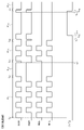
- FIG. 12 shows a timing chart of the detection unit operation according to the first embodiment.
- the times t A1 , t A2 , t A3 , t A4 and t A5 shall be visited in that order.
- Periods P A1 , P A2 , P A3 , P A4 , and P A5 in FIG. 12 are examples of the transmission period, braking period, first braking period, second braking period, and receiving period, respectively. The operation in each period will be specifically described below.
- a period from time t A1 to time t A2 is a transmission period P A1 during which the driving signal is supplied from the driving circuit 111 to the piezoelectric element 20 .
- the drive signal is supplied to the piezoelectric element 20 by the number of waves of the transmission wave.
- the wave number of the transmitted wave in the transmission period P A1 matches the number of cycles of the drive signal in the transmission period P A1 (that is, the quotient obtained by dividing the length of the transmission period P A1 by the length of the cycle of the drive signal).
- the number of transmitted waves in the transmission period P A1 has a predetermined value (for example, an integer of 2 or more) and is set based on data in a predetermined register of the storage circuit 131 .
- the wave number of the transmitted wave is "4", but the wave number of the transmitted wave may be arbitrary (the same applies to other embodiments described later).
- the transmission period P A1 ends.
- the drive circuit 111 Before the time t A1 , the drive circuit 111 is maintained in the initial state for a certain period of time . is started (the same applies to other embodiments described later). In the example of FIG. 12, the all-off state is assumed as the initial state. Good (similarly for other embodiments described later).
- a period from time t A2 to time t A3 is a braking period P A2 .
- the drive circuit 111 is maintained in the first braking state (ie transistors M1H and M2H are kept off and transistors M1L and M2L are kept on).
- time t A11 exists between time t A2 and time t A3
- drive circuit 111 is maintained in the first braking state from time t A2 to time t A11
- time t The drive circuit 111 is maintained in the fully off state from A11 to time tA3 .
- the drive circuit 111 is maintained in the first braking state from time t A2 to time t A3 .
- the drive circuit 111 is turned off until a predetermined minute time elapses from time t A2 , and the drive circuit 111 is turned off during a period from the time when the predetermined minute time has passed from time t A2 to time t A11 or t A3 .
- a modification in which the first braking state is maintained is also possible.
- a period from time t A3 to time t A4 is a first braking period P A3 during which a braking signal is supplied from the driving circuit 111 to the piezoelectric element 20 .
- the braking signal is supplied to the piezoelectric element 20 by the number of waves of the braking wave.
- the number of braking waves in the first braking period P A3 is obtained by dividing the number of periods of the braking signal in the first braking period P A3 (that is, the length of the first braking period P A3 by the length of the period of the braking signal). quotient).
- the wave number of the braking wave in the first braking period P A3 has a predetermined value (for example, an integer of 2 or more) and is set based on data in a predetermined register of the storage circuit 131 .
- the wave number of the braking wave is "2", but the wave number of the braking wave may be arbitrary (the same applies to other embodiments described later).
- the first braking period P A3 ends when the length (2/f) of two cycles of the braking signal has elapsed from time t A3 (that is, at time t A4 ).
- the supply of the braking signal to the piezoelectric element 20 is started by switching the state of the drive circuit 111 from the fully off state to the first application state at time t A3 . Therefore, the length of the braking period P A2 determines the phase ⁇ of the braking signal in the first braking period P A3 .
- the period from time t A4 to time t A5 is the second braking period P A4 .
- a method of continuously connecting the damping circuit 140 to the piezoelectric element 20 during the entire second damping period P A4 can also be adopted, but in the first embodiment, the damping circuit 140 is connected only during a part of the second damping period P A4 . are connected to the piezoelectric element 20 .
- the control circuit 130 switches the state of the drive circuit 111 from the second application state to the all-off state at time t A4 , and then at time t A12 after a predetermined first predetermined time from time t A4 . , the state of the drive circuit 111 is switched from the fully off state to the first brake state.
- the control circuit 130 switches the value of the control signal CNT2 from "0" to "1" at time tA13 , which is a second predetermined time after time tA12 .
- the control circuit 130 connects the damping circuit 140 to the piezoelectric element 20 by switching the switches 151 and 152 from off to on at time t A13 .
- the state in which the damping circuit 140 and the piezoelectric element 20 are disconnected changes to the state in which the damping circuit 140 and the piezoelectric element 20 are connected at time t A13 .
- the control circuit 130 switches the state of the drive circuit 111 from the first braking state to the fully off state at time t A14 after a predetermined third predetermined time from time t A13 .
- control circuit 130 switches the state of the drive circuit 111 from the fully off state to the first braking state at time t A15 after time t A14 , and switches the state of the drive circuit 111 from the fully off state to the first braking state at time t A16 after a predetermined fourth predetermined time from time t A15 .
- the value of the control signal CNT2 is switched from "1" to "0". That is, the control circuit 130 disconnects the damping circuit 140 from the piezoelectric element 20 by switching the switches 151 and 152 from ON to OFF at time t A16 .
- the state in which the damping circuit 140 and the piezoelectric element 20 are connected changes to the state in which the damping circuit 140 and the piezoelectric element 20 are disconnected.
- the control circuit 130 switches the state of the drive circuit 111 from the first brake state to the fully off state at time t A5 after a predetermined fifth predetermined time from time t A16 .
- a predetermined potential for example, ground potential
- the other is opened during the reception period P A5 starting at time t A5 . It is possible (the same may be applied to other embodiments described later). That is, for example, during the reception period P A5 , one of the transistors M2L and M1L may be turned on and the other may be turned off while the transistors M1H and M2H are turned off.
- the voltage value VEV of the envelope signal obtained by the receiving circuit 120 decreases from time tA4 .
- the control circuit 130 has a comparator (not shown) that compares the voltage value V EV with a predetermined threshold V TH and may set the time t A15 based on the comparison result of the comparator. That is, for example, the control circuit 130 sets the time t A15 to the time when the voltage value V EV transitions from a state higher than the predetermined threshold value V TH to a state lower than the predetermined threshold value V TH after the end of the first braking period PA3 .
- the receiving circuit 120 generates a detection signal based on the voltage signal between the input terminals IN1 and IN2 during the reception period set after time t A5 , and the control circuit 130 performs the above-described distance detection based on the detection signal during the reception period. processing and proximity detection processing can be performed.
- the control circuit 110 may switch the state of the drive circuit 111 to the first brake state immediately after the first drive signal P A3 ends. That is, the control circuit 110 may switch the state of the drive circuit 111 from the second application state to the first braking state at time t A4 (in this case, time t A4 and time t A12 indicate the same time). be interpreted as a thing).
- FIG. 13 shows a timing chart according to a comparative example different from the first embodiment.
- the drive circuit 111 is maintained in the fully off state between times tA2 and tA3 and between times tA4 and tA5 .
- a braking period P A2 is provided after the transmission period P A1 and before the first braking period P A3 , and during the braking period P A2 the transistors M1L and M2L are turned on to perform a braking operation. Therefore, unlike the reference example of FIG. 13, the reverberation energy of the piezoelectric element 20 (that is, the accumulated mechanical energy of the piezoelectric element 20) is released to the pattern having the ground potential in the braking period P A2 , or the transistors M1L and M2L and the piezoelectric element 20 are discharged. The energy is consumed in a current loop passing through the element 20, thereby reducing the reverberation time of the piezoelectric element 20.
- the damping signal is supplied from the drive circuit 111 to the piezoelectric element 20 after the supply of the drive signal to the piezoelectric element 20 is stopped, and the damping circuit 140 is connected to the piezoelectric element 20 after the supply of the braking signal is stopped ( This point also applies to the comparative example of FIG. 13). This is also expected to reduce reverberation quickly (that is, it is possible to keep the reverberation time low).
- control circuit 130 executes damper connection control to connect the damping circuit 140 to the piezoelectric element 20 with a unique flow after stopping the supply of the braking signal to the piezoelectric element 20 . That is, in the damper connection control, the control circuit 130 according to the first embodiment starts the braking operation (t A12 ) before connecting the damping circuit 140 to the piezoelectric element 20, and connects the damping circuit 140 and the piezoelectric element 20. After that, the braking operation is stopped and the drive circuit 111 is turned off (t A14 via t A13 ).
- the pulse-like output accompanying the turning on of the switches 151 and 152 is Noise may be added to the piezoelectric element 20 to prolong the reverberation.
- the damper connection control when the switches 151 and 152 are turned on, the potential at both ends of the piezoelectric element 20 is fixed to the ground potential, so the pulse-like noise accompanying the turn-on of the switches 151 and 152 is absorbed by the pattern having the ground potential. be done. As a result, superposition of noise on the piezoelectric element 20 is avoided, and an increase in reverberation time due to noise is avoided.
- control circuit 130 executes damper disconnection control that disconnects the damping circuit 140 from the piezoelectric element 20 in a unique flow. That is, in the damper disconnection control, the control circuit 130 according to the first embodiment starts the braking operation (t A15 ) before disconnecting the damping circuit 140 and the piezoelectric element 20, and disconnects the damping circuit 140 and the piezoelectric element 20. After disconnecting, brake operation is stopped (t A5 via t A16 ).
- the pulse-like output accompanying the turn off of the switches 151 and 152 is Noise may be added to the piezoelectric element 20 to re-increase the reduced reverberation energy.
- the potential at both ends of the piezoelectric element 20 is fixed to the ground potential when the switches 151 and 152 are turned off, so the pulse-like noise accompanying the turn-off of the switches 151 and 152 is absorbed by the pattern having the ground potential. be done. As a result, superposition of noise on the piezoelectric element 20 is avoided, and an increase in reverberation time due to noise is avoided.
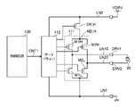
- a separation switch SW_L shown in FIG. 14 is added to the semiconductor device 10 in comparison with the first embodiment. That is, in the first embodiment, the sources of the transistors M1L and M2L are directly connected to the line LN1, whereas in the second embodiment, the node ND_L to which the sources of the transistors M1L and M2L are commonly connected and the line A separation switch SW_L is inserted between LN1 and . One end of the separation switch SW_L is connected to the node ND_L, and the other end of the separation switch SW_L is connected to the line LN1 to which the ground potential is applied.
- the separation switch SW_L may be an arbitrary switching element, but here, the separation switch SW_L is configured with an N-channel MOSFET, and the N-channel MOSFET as the separation switch SW_L is also denoted by the symbol "SW_L ” is used to refer to the transistor SW_L. Turning on the separation switch SW_L and turning on the transistor SW_L are synonymous with each other, and turning off the separation switch SW_L and turning off the transistor SW_L are synonymous with each other.
- the drain of transistor SW_L is connected to node ND_L, and the source of transistor SW_L is connected to line LN1 to which the ground potential is applied.
- the gate driver 112 controls the gate potentials of the transistors M1H, M1L, M2H and M2L and SW_L according to the control signal CNT1 supplied from the control circuit 130, thereby turning the transistors M1H, M1L, M2H and M2L and SW_L on/off. Control the states individually.
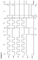
- FIG. 15 shows a timing chart of the detection unit operation according to the second embodiment.
- the timing chart of FIG. 15 is obtained by adding state transitions of the separation switch SW_L to the timing chart of FIG. Except for the separation switch SW_L, the content and flow of the detection unit operation are as shown in the first embodiment, so in the second embodiment, unless necessary, only the operation of the separation switch SW_L will be described.
- the separation switch SW_L is kept on until time t A2 and kept off during the braking period P A2 between times t A2 and t A3 .
- the isolation switch SW_L is kept on during a first braking period P A3 between times t A3 and t A4 and a reception period P A5 after time t A5 .
- the separation switch SW_L is turned on between times tA4 and tA12
- the separation switch SW_L is turned off between times tA12 and tA5 .
- the separation switch SW_L may be kept on during the entire second damping period P A4 between times t A4 and t A5 .
- the separation switch SW_L is turned off when the braking operation is performed in the braking period P A2 (when both the transistors M1L and M2L are on).
- a current loop is formed via the transistors M1L and M2L separated from the ground pattern and the piezoelectric element 20, and the current loop contains the reverberation energy of the piezoelectric element 20 (that is, the reverberation energy of the piezoelectric element 20).
- the reverberation energy of the piezoelectric element 20 can be effectively consumed by the flow of current based on the accumulated mechanical energy.
- the current based on the reverberant energy of the piezoelectric element 20 may flow into the ground pattern during the brake period P A2 depending on the relationship between the transistors M1L and M2L and the ground pattern.
- Such current wraparound can somewhat degrade the effective reduction of reverberation, and can also have undesirable effects on other circuits connected to the ground trace. According to the second embodiment, these concerns are resolved.
- the separation switch SW_L is turned off during the entire period during which the braking operation is performed during the braking period P A2 (the period during which both the transistors M1L and M2L are turned on). .
- the separation switch SW_L may be kept off only during a part of the period during which the braking operation is performed. For example, as shown in FIG. 16, in the detection unit operation, the separation switch SW_L is kept on from time t A2 to time t A2 ' after a predetermined minute time, and from time t A2 ' to time t A3 thereafter. During this period, the separation switch SW_L may be kept off. After time t A3 , it is as described above.
- the structures of the transistors M1L and M2L are changed so that the impedance between the first end and the second end of the piezoelectric element 20 (impedance at frequency f) and the total value of the on-resistances of the transistors M1L and M2L are the same. You may make it decide. As a result, the consumption of the reverberation energy of the piezoelectric element 20 due to the braking operation can be maximized, and the reverberation can be quickly reduced.
- FIG. 17 shows a timing chart of the detection unit operation according to the third embodiment.
- the drive circuit 111 is set and held in the second braking state (see FIG. 4) during braking.
- the third embodiment is the same as the first embodiment, except that the state of the drive circuit 111 is changed from the first braking state to the second braking state in the braking operation based on the first embodiment.
- the drive circuit 111 is maintained in the second braking state (that is, the transistors M1H and M2H are kept on and the transistors M1L and M2L are kept off) during all or part of the braking period P A2 . ). Therefore, in the first embodiment, the period during which the drive circuit 111 is set to the first braking state (the period between times tA2 and tA11 in the example of FIG. 12) in the braking period P A2 in the third embodiment. is replaced during the period in which the drive circuit 111 is set to the second brake state (the period between times t A2 and t A11 in the example of FIG. 17) (this replacement is referred to as first replacement).
- the period during which the drive circuit 111 is set to the first braking state is the period during which the drive circuit 111 is set to the second brake state in the third embodiment (in the example of FIG. 17, the period between times tA12 and tA14 and the period between times tA15 and tA5 ).
- this substitution is called the second substitution. That is, the damper connection control and damper disconnection control described in the first embodiment are also performed in the third embodiment. is set and held at
- a fourth embodiment will be described.
- the fourth embodiment is obtained by adding an applied technology to the third embodiment, and the description of the third embodiment is also applied to the fourth embodiment for matters not specifically described in the fourth embodiment.
- the fourth embodiment is obtained by modifying the third embodiment in the same manner as the modification from the first embodiment to the second embodiment.
- a separation switch SW_H shown in FIG. 18 is added to the semiconductor device 10 in comparison with the first and third embodiments. That is, in the first and third embodiments, the sources of the transistors M1H and M2H are directly connected to the line LN2. and the line LN2, a separation switch SW_H is inserted. One end of separation switch SW_H is connected to node ND_H, and the other end of separation switch SW_H is connected to line LN2 to which driving power supply voltage VDRV is applied.
- the separation switch SW_H may be any switching element, but here, the separation switch SW_H is composed of a P-channel MOSFET, and the P-channel MOSFET as the separation switch SW_H is also denoted by the symbol "SW_H". ” is used to refer to the transistor SW_H. Turning on the separation switch SW_H and turning on the transistor SW_H are synonymous with each other, and turning off the separation switch SW_H and turning off the transistor SW_H are synonymous with each other.
- the drain of transistor SW_H is connected to node ND_H, and the source of transistor SW_H is connected to line LN2 to which drive power supply voltage VDRV is applied.
- the gate driver 112 controls the gate potentials of the transistors M1H, M1L, M2H and M2L, and SW_H according to the control signal CNT1 supplied from the control circuit 130, thereby turning the transistors M1H, M1L, M2H, M2L, and SW_H on/off. Control the states individually.
- FIG. 19 shows a timing chart of the detection unit operation according to the fourth embodiment.
- the state control (on/off control) of the separation switch SW_H in the fourth embodiment is the same as the state control (on/off control) of the separation switch SW_L in the second embodiment.
- the description of SW_L state control also applies to the fourth embodiment. In this application, it is sufficient to replace the separation switch SW_L in the second embodiment with the separation switch SW_H in the fourth embodiment. Similar to the modification from FIG. 15 to FIG. 16 described in the second embodiment, modification from FIG. 19 to FIG. 20 is also possible.
- the separation switch SW_H is turned off. is turned off.
- the separation switch SW_H is kept on during the transmission period P A1 , the first braking period P A3 and the reception period P A5 .
- the separation switch SW_H is turned off between times t A12 and t A5 , but the separation switch SW_H may be kept on throughout the second braking period P A4 .
- the transistor M1H and The structure of M2H may be determined. As a result, the consumption of the reverberation energy of the piezoelectric element 20 due to the braking operation can be maximized, and the reverberation can be quickly reduced.
- the ultrasonic sensor 1 can be mounted on any device.
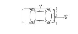
- one or more ultrasonic sensors 1 may be installed in a vehicle CR such as an automobile.
- four ultrasonic sensors 1 are installed in the rear part of the vehicle body of the vehicle CR. example) can perform distance detection processing and approach detection processing.
- the upper block 2 may be an ECU (Electronic Control Unit) mounted on the vehicle CR.
- ECU Electronic Control Unit
- N-channel FETs are changed to P-channel FETs, or P-channel FETs are changed to N-channel FETs.
- the configuration of circuits containing FETs can be varied, as can any type of FET.
- any of the transistors described above may be any type of transistor as long as there is no inconvenience.
- any transistor described above as a MOSFET can be replaced with a junction FET, an IGBT (Insulated Gate Bipolar Transistor), or a bipolar transistor as long as it does not cause any inconvenience.
- Any transistor has a first electrode, a second electrode and a control electrode.
- a FET one of the first and second electrodes is the drain and the other is the source, and the control electrode is the gate.
- an IGBT one of the first and second electrodes is the collector and the other is the emitter, and the control electrode is the gate.
- a bipolar transistor not belonging to an IGBT one of the first and second electrodes is the collector and the other is the emitter and the control electrode is the base.
- a semiconductor device (10; see FIG. 3) is capable of supplying a drive signal in an ultrasonic band to a piezoelectric element (20), and after stopping supply of the drive signal, the phase of the drive signal and A drive circuit (111) configured to be able to supply braking signals having different phases to the piezoelectric element; and a control circuit (130) configured to be able to control the drive circuit.
- a full bridge circuit is provided between line 1 (LN1) and a second line (LN2) to which a potential higher than that of the first line is applied, based on the potential difference between the first line and the second line.
- the driving signal and the braking signal can be supplied to the piezoelectric element using the full bridge circuit, and the full bridge circuit includes a first switch (M1H) provided on the second line side and the first switch (M1H) provided on the side of the second line.
- the control circuit causes the drive circuit to perform a braking operation after stopping supply of the drive signal to the piezoelectric element and before supplying the braking signal to the piezoelectric element. (see FIG. 12 or 17), and in the braking operation, the first switch and the third switch are turned off and the second switch and the fourth switch are turned on, or the first switch and the third switch are turned on and the second switch and the fourth switch are turned off (first configuration).
- the reverberant energy of the piezoelectric element based on the drive signal (that is, the accumulated mechanical energy of the piezoelectric element) is released to the pattern of the first or second line, or via the second and fourth switches and the piezoelectric element. or the current loop passing through the first and third switches and the piezoelectric element, thereby reducing the reverberation time of the piezoelectric element.
- a separation switch SW_L inserted between a connection node between the second switch and the fourth switch and the first line is further provided.
- the control circuit keeps the separation switch ON during the period of supplying the driving signal to the piezoelectric element and the period of supplying the braking signal to the piezoelectric element, and the braking operation causes the first switch and the third switch to close.
- a configuration may be employed in which the separation switch is kept off during at least part of the period in which the second switch and the fourth switch are off and the second switch and the fourth switch are on.
- a current loop is formed through the piezoelectric element and the second and fourth switches isolated from the first line, and the reverberation energy of the piezoelectric element (ie, the piezoelectric element) is formed in the current loop.
- the reverberation energy of the piezoelectric element can be effectively consumed by the flow of current based on the accumulated mechanical energy of the element.
- a separation switch (SW_H) inserted between a connection node between the first switch and the third switch and the second line is further provided.
- the control circuit keeps the separation switch ON during the period of supplying the driving signal to the piezoelectric element and the period of supplying the braking signal to the piezoelectric element, and the braking operation causes the first switch and the third switch to close.
- a configuration (third configuration) may be employed in which the separation switch is kept off during at least a part of the period in which the second switch and the fourth switch are on and the second switch and the fourth switch are off.
- a current loop is formed via the piezoelectric element and the first and third switches isolated from the second line, and the reverberation energy of the piezoelectric element (i.e., piezoelectric).
- the reverberation energy of the piezoelectric element can be effectively consumed by the flow of current based on the accumulated mechanical energy of the element.
- the semiconductor device comprises a damping circuit (140) having a resistive load (141) and an inductive load (142), wherein the control circuit a configuration configured so that the damping circuit can be connected to the piezoelectric element after the braking signal is supplied from the driving circuit to the piezoelectric element through the braking operation after stopping the supply of the driving signal to the piezoelectric element; (Fourth configuration).
- the reverberation of the piezoelectric element can be reduced.
- the damping signal is effective in reducing reverberation in areas where the reverberation amplitude (amplitude of the piezoelectric element due to reverberation) is high, but when the reverberation amplitude decreases, the damping signal itself becomes a factor of new reverberation. Sometimes.
- the reverberation can be reduced through absorption of mechanical energy by the piezoelectric element.
- a resistive load or an inductive load exhibits a relatively high reverberation reduction effect when the reverberation amplitude is small, but the reverberation reduction effect is relatively low when the reverberation amplitude is large due to circuit voltage restrictions, etc. has now been obtained by the inventor.
- reverberation can be quickly reduced (that is, reverberation time can be kept low).
- the control circuit connects the damper after stopping the supply of the braking signal to the piezoelectric element (after tA4 ).
- the damper connection control the braking operation is started before the damping circuit is connected to the piezoelectric element, and the braking operation is started after the damping circuit and the piezoelectric element are connected.
- a configuration (fifth configuration) in which the first to fourth switches are all turned off by stopping may be employed.
- damper connection control According to the damper connection control, superimposition of noise on the piezoelectric element that may occur when the damping circuit and the piezoelectric element are switched from the disconnected state to the connected state is avoided. As a result, an increase in reverberation time due to noise is avoided.
- the control circuit controls the damper after stopping the supply of the braking signal to the piezoelectric element (after tA4 ).
- damper disconnection control can be executed, and in the damper disconnection control, before disconnection between the damping circuit and the piezoelectric element.
- a configuration (sixth configuration) may be employed in which the braking operation is started, and after disconnection between the damping circuit and the piezoelectric element is stopped, the braking operation is stopped.
- damper disconnection control According to the damper disconnection control, superimposition of noise on the piezoelectric element that may occur when the damping circuit and the piezoelectric element are switched from the connected state to the disconnected state is avoided. As a result, an increase in reverberation time due to noise is avoided.
- the damping circuit may have a configuration (seventh configuration) in which the resistive load and the inductive load are connected in parallel.
- An ultrasonic sensor includes a semiconductor device according to any one of the first to seventh configurations, and a piezoelectric element connected to the semiconductor device (eighth configuration). .
Landscapes
- Engineering & Computer Science (AREA)
- Radar, Positioning & Navigation (AREA)
- Remote Sensing (AREA)
- Physics & Mathematics (AREA)
- Computer Networks & Wireless Communication (AREA)
- General Physics & Mathematics (AREA)
- Acoustics & Sound (AREA)
- Mechanical Engineering (AREA)
- Measurement Of Velocity Or Position Using Acoustic Or Ultrasonic Waves (AREA)
Abstract
Description
第1実施例を説明する。第1実施例では、ブレーキ動作において駆動回路111を第1ブレーキ状態(図4参照)に設定及び保持する。
第2実施例を説明する。第2実施例は第1実施例に応用技術を付加したものであり、第2実施例において特に述べない事項については、第1実施例の記載が第2実施例にも適用される。
第3実施例を説明する。図17に第3実施例に係る検出単位動作のタイミングチャートを示す。第3実施例では、ブレーキ動作において駆動回路111を第2ブレーキ状態(図4参照)に設定及び保持する。第1実施例を基準に、ブレーキ動作での駆動回路111の状態が第1ブレーキ状態から第2ブレーキ状態に変形される点を除き、第3実施例は第1実施例と同様である。
第4実施例を説明する。第4実施例は第3実施例に応用技術を付加したものであり、第4実施例において特に述べない事項については、第3実施例の記載が第4実施例にも適用される。第4実施例は、第1実施例から第2実施例への変形と同様の変形を第3実施例に施したものである。
第5実施例を説明する。第5実施例では、上述の各技術に対する応用技術、変形技術及び補足事項等を説明する。
上述の実施形態にて具体的構成例が示された本開示について付記を設ける。
2 上位ブロック
10 半導体装置
11 送信回路
12 受信回路
13 制御回路
20 圧電素子
W1 出力波信号
W2 反射波信号
111 駆動回路
112 ゲートドライバ
120 受信回路
130 制御回路
140 ダンピング回路
141 抵抗負荷
142 誘導負荷
150 スイッチ回路
160 内部電源回路
M1H、M1L、M2H、M2L トランジスタ(第1~第4スイッチ)
SW_L、SW_H 分離スイッチ
Claims (8)
- 圧電素子に超音波帯域の駆動信号を供給可能であって、前記駆動信号の供給停止後に前記駆動信号の位相と異なる位相を有する制動信号を前記圧電素子に供給可能に構成された駆動回路と、
前記駆動回路を制御可能に構成された制御回路と、を備え、
前記駆動回路は、第1ラインと前記第1ラインよりも高い電位が加わるべき第2ラインとの間に設けられたフルブリッジ回路を備え、前記第1ライン及び前記第2ライン間の電位差に基づき前記フルブリッジ回路を用いて前記駆動信号及び前記制動信号を前記圧電素子に供給可能に構成され、
前記フルブリッジ回路は、前記第2ライン側に設けられた第1スイッチと前記第1ライン側に設けられた第2スイッチとの直列回路、及び、前記第2ライン側に設けられた第3スイッチと前記第1ライン側に設けられた第4スイッチとの直列回路を有して、前記第1スイッチ及び前記第2スイッチ間の接続ノード、前記第3スイッチ及び前記第4スイッチ間の接続ノードを、夫々、前記圧電素子の第1端、第2端に接続可能に構成され、
前記制御回路は、前記圧電素子への前記駆動信号の供給を停止してから前記制動信号を前記圧電素子に供給する前にブレーキ動作を前記駆動回路に行わせることが可能に構成され、
前記ブレーキ動作では、前記第1スイッチ及び第3スイッチがオフ且つ前記第2スイッチ及び第4スイッチがオンとされる、又は、前記第1スイッチ及び第3スイッチがオン且つ前記第2スイッチ及び第4スイッチがオフとされる
、半導体装置。 - 前記第2スイッチ及び前記第4スイッチ間の接続ノードと前記第1ラインとの間に挿入された分離スイッチを更に備え、
前記制御回路は、前記圧電素子に対する前記駆動信号の供給期間及び前記圧電素子に対する前記制動信号の供給期間において前記分離スイッチをオンに保ち、前記ブレーキ動作により前記第1スイッチ及び第3スイッチがオフ且つ前記第2スイッチ及び第4スイッチがオンとされる期間の少なくとも一部において前記分離スイッチをオフに保つ
、請求項1に記載の半導体装置。 - 前記第1スイッチ及び前記第3スイッチ間の接続ノードと前記第2ラインとの間に挿入された分離スイッチを更に備え、
前記制御回路は、前記圧電素子に対する前記駆動信号の供給期間及び前記圧電素子に対する前記制動信号の供給期間において前記分離スイッチをオンに保ち、前記ブレーキ動作により前記第1スイッチ及び第3スイッチがオン且つ前記第2スイッチ及び第4スイッチがオフとされる期間の少なくとも一部において前記分離スイッチをオフに保つ
、請求項1に記載の半導体装置。 - 抵抗負荷及び誘導負荷を有するダンピング回路と、備え、
前記制御回路は、前記圧電素子への前記駆動信号の供給停止後に前記ブレーキ動作を経て前記駆動回路より前記制動信号を前記圧電素子に供給させた後、前記ダンピング回路を前記圧電素子に接続可能に構成される
、請求項1~3の何れかに記載の半導体装置。 - 前記制御回路は、前記圧電素子への前記制動信号の供給停止後、ダンパー接続制御を実行可能に構成され、前記ダンパー接続制御において、前記ダンピング回路を前記圧電素子に接続する前に前記ブレーキ動作を開始し、前記ダンピング回路及び前記圧電素子間を接続してから前記ブレーキ動作を停止して前記第1~第4スイッチを全てオフとする
、請求項4に記載の半導体装置。 - 前記制御回路は、前記圧電素子への前記制動信号の供給停止後、前記ダンパー接続制御により前記ダンピング回路及び前記圧電素子間を接続した後にダンパー切り離し制御を実行可能に構成され、前記ダンパー切り離し制御において、前記ダンピング回路及び前記圧電素子間を遮断する前に前記ブレーキ動作を開始し、前記ダンピング回路及び前記圧電素子間を遮断してから前記ブレーキ動作を停止する
、請求項5に記載の半導体装置。 - 前記ダンピング回路において前記抵抗負荷と前記誘導負荷は並列接続される
、請求項4~6の何れかに記載の半導体装置。 - 請求項1~7の何れかに記載の半導体装置と、
前記半導体装置に接続される圧電素子と、を備えた
、超音波センサ。
Priority Applications (3)
| Application Number | Priority Date | Filing Date | Title |
|---|---|---|---|
| CN202180095905.XA CN116981960A (zh) | 2021-03-23 | 2021-12-20 | 半导体装置以及超声波传感器 |
| JP2023508627A JPWO2022201681A1 (ja) | 2021-03-23 | 2021-12-20 | |
| US18/469,006 US20240004048A1 (en) | 2021-03-23 | 2023-09-18 | Semiconductor device and ultrasonic sensor |
Applications Claiming Priority (2)
| Application Number | Priority Date | Filing Date | Title |
|---|---|---|---|
| JP2021-048769 | 2021-03-23 | ||
| JP2021048769 | 2021-03-23 |
Related Child Applications (1)
| Application Number | Title | Priority Date | Filing Date |
|---|---|---|---|
| US18/469,006 Continuation US20240004048A1 (en) | 2021-03-23 | 2023-09-18 | Semiconductor device and ultrasonic sensor |
Publications (1)
| Publication Number | Publication Date |
|---|---|
| WO2022201681A1 true WO2022201681A1 (ja) | 2022-09-29 |
Family
ID=83396657
Family Applications (1)
| Application Number | Title | Priority Date | Filing Date |
|---|---|---|---|
| PCT/JP2021/046960 Ceased WO2022201681A1 (ja) | 2021-03-23 | 2021-12-20 | 半導体装置及び超音波センサ |
Country Status (4)
| Country | Link |
|---|---|
| US (1) | US20240004048A1 (ja) |
| JP (1) | JPWO2022201681A1 (ja) |
| CN (1) | CN116981960A (ja) |
| WO (1) | WO2022201681A1 (ja) |
Families Citing this family (2)
| Publication number | Priority date | Publication date | Assignee | Title |
|---|---|---|---|---|
| WO2024011519A1 (zh) * | 2022-07-14 | 2024-01-18 | 深圳市汇顶科技股份有限公司 | 超声波指纹检测装置和电子设备 |
| EP4699709A1 (de) * | 2024-08-21 | 2026-02-25 | Elmos Semiconductor SE | Vorrichtung zur ansteuerung eines ultraschall-transducers zur erzeugung von ultraschallwellen |
Citations (4)
| Publication number | Priority date | Publication date | Assignee | Title |
|---|---|---|---|---|
| US20110026365A1 (en) * | 2009-07-30 | 2011-02-03 | Lite-On It Corp. | Ultrasonic transducer and signal decay time adjusting method applied thereto |
| CN201788278U (zh) * | 2010-09-10 | 2011-04-06 | 无锡市海鹰加科海洋技术有限责任公司 | 测深仪大功率声波发射装置 |
| US20160284967A1 (en) * | 2015-03-24 | 2016-09-29 | Freescale Semiconductor, Inc. | Pulse generator for energizing an ultrasonic transducer, a method of operating the pulse generator and a ultrasonic distance sensing system |
| WO2020008868A1 (ja) * | 2018-07-06 | 2020-01-09 | 株式会社村田製作所 | 超音波センサ |
Family Cites Families (24)
| Publication number | Priority date | Publication date | Assignee | Title |
|---|---|---|---|---|
| JP4178637B2 (ja) * | 1998-12-25 | 2008-11-12 | 松下電工株式会社 | 超音波センサの送受波回路 |
| JP4195276B2 (ja) * | 2002-11-27 | 2008-12-10 | 古野電気株式会社 | 超音波送信装置、超音波送受信装置およびソナー装置 |
| JP4216647B2 (ja) * | 2003-05-29 | 2009-01-28 | 古野電気株式会社 | 超音波送信装置、超音波送受信装置、および探知装置 |
| JP2009058298A (ja) * | 2007-08-30 | 2009-03-19 | Denso Corp | 超音波センサ |
| CN103988327B (zh) * | 2011-12-09 | 2016-11-16 | 株式会社村田制作所 | 压电元件用驱动电路 |
| DE102011089542A1 (de) * | 2011-12-22 | 2013-06-27 | Robert Bosch Gmbh | Verfahren und Schaltungsanordnung zur Ansteuerung eines Ultraschallsensors |
| JP6041901B2 (ja) * | 2012-12-21 | 2016-12-14 | 三菱電機株式会社 | 超音波送受信装置 |
| WO2014166835A1 (de) * | 2013-04-08 | 2014-10-16 | Elmos Semiconductor Ag | Verfahren zur messung mittels ultraschall, insbesondere als parkhilfe für fahrzeuge, und ultraschallmesssysteme |
| DE102014107311A1 (de) * | 2014-05-23 | 2015-11-26 | Valeo Schalter Und Sensoren Gmbh | Verfahren zum Betreiben eines Ultraschallsensors eines Kraftfahrzeugs, Ultraschallsensorvorrichtung, Fahrerassistenzsystem sowie Kraftfahrzeug |
| US10165358B2 (en) * | 2014-12-11 | 2018-12-25 | Semiconductor Components Industries, Llc | Transducer controller and method therefor |
| JP6200461B2 (ja) * | 2015-07-14 | 2017-09-20 | ファナック株式会社 | ダイナミックブレーキ回路を有するモータ駆動装置 |
| US10585178B2 (en) * | 2015-10-21 | 2020-03-10 | Semiconductor Componenents Industries, Llc | Piezo transducer controller and method having adaptively-tuned linear damping |
| EP3208634B1 (de) * | 2016-02-17 | 2018-08-15 | ELMOS Semiconductor Aktiengesellschaft | Ultraschallmesssystem, insbesondere zur abstandsmessung und/oder als parkhilfe bei fahrzeugen |
| JP6765069B2 (ja) * | 2016-03-15 | 2020-10-07 | パナソニックIpマネジメント株式会社 | 物体検知装置 |
| DE102017207679A1 (de) * | 2017-05-08 | 2018-11-08 | Robert Bosch Gmbh | Betriebsverfahren und Steuereinheit für eine Ultraschallsendeempfangseinrichtung, Ultraschallsendeempfangseinrichtung und Arbeitsvorrichtung |
| JP2019012955A (ja) * | 2017-06-30 | 2019-01-24 | ローム株式会社 | 超音波センサ駆動回路 |
| US10923297B2 (en) * | 2017-08-24 | 2021-02-16 | Rohm Co., Ltd. | Switch monitoring device, switch state detection circuit, and a vehicle-mounted switch system |
| US11269067B2 (en) * | 2017-09-12 | 2022-03-08 | Semiconductor Components Industries, Llc | Response-based determination of piezoelectric transducer state |
| US11194028B2 (en) * | 2017-09-12 | 2021-12-07 | Semiconductor Components Industries, Llc | Measuring resonance parameters of piezoelectric transducers |
| JP7167495B2 (ja) * | 2018-06-12 | 2022-11-09 | 株式会社アイシン | 物体検知装置および物体検知システム |
| DE102019126919A1 (de) * | 2019-10-08 | 2021-04-08 | Valeo Schalter Und Sensoren Gmbh | Verfahren zum Erfassen eines Objekts in einem Nahbereich auf Grundlage einer Energie des Sensorsignals, Recheneinrichtung sowie Ultraschallsensorvorrichtung |
| US11405730B2 (en) * | 2020-05-08 | 2022-08-02 | Semiconductor Components Industries, Llc | Multichannel minimum distance chirp echo detection |
| CN111510018B (zh) * | 2020-05-20 | 2022-05-24 | 矽力杰半导体技术(杭州)有限公司 | 压电驱动电路和压电驱动方法 |
| US12178134B2 (en) * | 2021-02-10 | 2024-12-24 | Cirrus Logic Inc. | Driver circuitry |
-
2021
- 2021-12-20 WO PCT/JP2021/046960 patent/WO2022201681A1/ja not_active Ceased
- 2021-12-20 JP JP2023508627A patent/JPWO2022201681A1/ja active Pending
- 2021-12-20 CN CN202180095905.XA patent/CN116981960A/zh active Pending
-
2023
- 2023-09-18 US US18/469,006 patent/US20240004048A1/en active Pending
Patent Citations (4)
| Publication number | Priority date | Publication date | Assignee | Title |
|---|---|---|---|---|
| US20110026365A1 (en) * | 2009-07-30 | 2011-02-03 | Lite-On It Corp. | Ultrasonic transducer and signal decay time adjusting method applied thereto |
| CN201788278U (zh) * | 2010-09-10 | 2011-04-06 | 无锡市海鹰加科海洋技术有限责任公司 | 测深仪大功率声波发射装置 |
| US20160284967A1 (en) * | 2015-03-24 | 2016-09-29 | Freescale Semiconductor, Inc. | Pulse generator for energizing an ultrasonic transducer, a method of operating the pulse generator and a ultrasonic distance sensing system |
| WO2020008868A1 (ja) * | 2018-07-06 | 2020-01-09 | 株式会社村田製作所 | 超音波センサ |
Also Published As
| Publication number | Publication date |
|---|---|
| US20240004048A1 (en) | 2024-01-04 |
| JPWO2022201681A1 (ja) | 2022-09-29 |
| CN116981960A (zh) | 2023-10-31 |
Similar Documents
| Publication | Publication Date | Title |
|---|---|---|
| JP5537270B2 (ja) | 出力回路 | |
| JP4235561B2 (ja) | 半ブリッジ駆動回路とその駆動回路を備える電力変換システム | |
| US20240004048A1 (en) | Semiconductor device and ultrasonic sensor | |
| JP5114818B2 (ja) | 電流検出方法、電流検出回路及び過電流保護回路 | |
| EP1119900A1 (en) | Methods and apparatus for reducing mosfet body diode conduction in a half-bridge configuration | |
| JP2021535723A (ja) | スイッチング電力コンバータのハイサイド制御の促進 | |
| KR987000733A (ko) | Cmos 출력 버퍼내에서 전압 발진을 감소시킬 음 피드백 장치(negative feedback to reduce voltage oscillation in cmos output buffers) | |
| CN108494394B (zh) | 一种低噪声且抗高地弹噪声的输出驱动电路及方法 | |
| US20240001404A1 (en) | Semiconductor device and ultrasonic sensor | |
| KR100449950B1 (ko) | 부하구동력 가변형 증폭회로 | |
| CN104426480A (zh) | 半导体集成电路以及振荡系统 | |
| JP5219867B2 (ja) | Btl回路 | |
| JP2004056211A (ja) | 半導体装置およびd級増幅器 | |
| JP5365136B2 (ja) | 電力変換装置の駆動装置 | |
| WO2023234168A1 (ja) | 圧電素子制御装置及び超音波センサ | |
| US10348276B2 (en) | Loop delay optimization for multi-voltage self-synchronous systems | |
| US12483244B2 (en) | Buffer with reduced shoot-through current | |
| JP4222389B2 (ja) | リンギング低減回路および該リンギング低減回路を備えた半導体集積回路 | |
| US11791820B2 (en) | Output circuit, transmission circuit, and semiconductor integrated circuit | |
| KR100765875B1 (ko) | 신호를 저전압 영역에서 고전압 영역으로 변환시키는 방법및 회로 | |
| JP2008295103A (ja) | リンギング低減回路および該リンギング低減回路を備えた半導体集積回路 | |
| JP2830902B2 (ja) | 出力バッファ回路 | |
| JPH088709A (ja) | ブリッジ制御回路 | |
| JP2021190894A (ja) | ゲートドライバ装置 | |
| JP2013074537A (ja) | コンパレータおよびそれを用いたdc/dcコンバータの制御回路、電子機器 |
Legal Events
| Date | Code | Title | Description |
|---|---|---|---|
| 121 | Ep: the epo has been informed by wipo that ep was designated in this application |
Ref document number: 21933273 Country of ref document: EP Kind code of ref document: A1 |
|
| WWE | Wipo information: entry into national phase |
Ref document number: 2023508627 Country of ref document: JP |
|
| WWE | Wipo information: entry into national phase |
Ref document number: 202180095905.X Country of ref document: CN |
|
| NENP | Non-entry into the national phase |
Ref country code: DE |
|
| 122 | Ep: pct application non-entry in european phase |
Ref document number: 21933273 Country of ref document: EP Kind code of ref document: A1 |