WO2020008868A1 - 超音波センサ - Google Patents
超音波センサ Download PDFInfo
- Publication number
- WO2020008868A1 WO2020008868A1 PCT/JP2019/024172 JP2019024172W WO2020008868A1 WO 2020008868 A1 WO2020008868 A1 WO 2020008868A1 JP 2019024172 W JP2019024172 W JP 2019024172W WO 2020008868 A1 WO2020008868 A1 WO 2020008868A1
- Authority
- WO
- WIPO (PCT)
- Prior art keywords
- variable
- circuit
- operational amplifier
- ultrasonic sensor
- signal
- Prior art date
Links
Images


Classifications
-
- B—PERFORMING OPERATIONS; TRANSPORTING
- B06—GENERATING OR TRANSMITTING MECHANICAL VIBRATIONS IN GENERAL
- B06B—METHODS OR APPARATUS FOR GENERATING OR TRANSMITTING MECHANICAL VIBRATIONS OF INFRASONIC, SONIC, OR ULTRASONIC FREQUENCY, e.g. FOR PERFORMING MECHANICAL WORK IN GENERAL
- B06B1/00—Methods or apparatus for generating mechanical vibrations of infrasonic, sonic, or ultrasonic frequency
- B06B1/02—Methods or apparatus for generating mechanical vibrations of infrasonic, sonic, or ultrasonic frequency making use of electrical energy
- B06B1/0207—Driving circuits
- B06B1/0215—Driving circuits for generating pulses, e.g. bursts of oscillations, envelopes
-
- G—PHYSICS
- G01—MEASURING; TESTING
- G01S—RADIO DIRECTION-FINDING; RADIO NAVIGATION; DETERMINING DISTANCE OR VELOCITY BY USE OF RADIO WAVES; LOCATING OR PRESENCE-DETECTING BY USE OF THE REFLECTION OR RERADIATION OF RADIO WAVES; ANALOGOUS ARRANGEMENTS USING OTHER WAVES
- G01S7/00—Details of systems according to groups G01S13/00, G01S15/00, G01S17/00
- G01S7/52—Details of systems according to groups G01S13/00, G01S15/00, G01S17/00 of systems according to group G01S15/00
- G01S7/521—Constructional features
-
- G—PHYSICS
- G01—MEASURING; TESTING
- G01S—RADIO DIRECTION-FINDING; RADIO NAVIGATION; DETERMINING DISTANCE OR VELOCITY BY USE OF RADIO WAVES; LOCATING OR PRESENCE-DETECTING BY USE OF THE REFLECTION OR RERADIATION OF RADIO WAVES; ANALOGOUS ARRANGEMENTS USING OTHER WAVES
- G01S7/00—Details of systems according to groups G01S13/00, G01S15/00, G01S17/00
- G01S7/52—Details of systems according to groups G01S13/00, G01S15/00, G01S17/00 of systems according to group G01S15/00
- G01S7/523—Details of pulse systems
- G01S7/524—Transmitters
-
- G—PHYSICS
- G01—MEASURING; TESTING
- G01S—RADIO DIRECTION-FINDING; RADIO NAVIGATION; DETERMINING DISTANCE OR VELOCITY BY USE OF RADIO WAVES; LOCATING OR PRESENCE-DETECTING BY USE OF THE REFLECTION OR RERADIATION OF RADIO WAVES; ANALOGOUS ARRANGEMENTS USING OTHER WAVES
- G01S7/00—Details of systems according to groups G01S13/00, G01S15/00, G01S17/00
- G01S7/52—Details of systems according to groups G01S13/00, G01S15/00, G01S17/00 of systems according to group G01S15/00
- G01S7/523—Details of pulse systems
- G01S7/526—Receivers
-
- H—ELECTRICITY
- H04—ELECTRIC COMMUNICATION TECHNIQUE
- H04R—LOUDSPEAKERS, MICROPHONES, GRAMOPHONE PICK-UPS OR LIKE ACOUSTIC ELECTROMECHANICAL TRANSDUCERS; DEAF-AID SETS; PUBLIC ADDRESS SYSTEMS
- H04R3/00—Circuits for transducers, loudspeakers or microphones
-
- B—PERFORMING OPERATIONS; TRANSPORTING
- B06—GENERATING OR TRANSMITTING MECHANICAL VIBRATIONS IN GENERAL
- B06B—METHODS OR APPARATUS FOR GENERATING OR TRANSMITTING MECHANICAL VIBRATIONS OF INFRASONIC, SONIC, OR ULTRASONIC FREQUENCY, e.g. FOR PERFORMING MECHANICAL WORK IN GENERAL
- B06B2201/00—Indexing scheme associated with B06B1/0207 for details covered by B06B1/0207 but not provided for in any of its subgroups
- B06B2201/30—Indexing scheme associated with B06B1/0207 for details covered by B06B1/0207 but not provided for in any of its subgroups with electronic damping
-
- B—PERFORMING OPERATIONS; TRANSPORTING
- B06—GENERATING OR TRANSMITTING MECHANICAL VIBRATIONS IN GENERAL
- B06B—METHODS OR APPARATUS FOR GENERATING OR TRANSMITTING MECHANICAL VIBRATIONS OF INFRASONIC, SONIC, OR ULTRASONIC FREQUENCY, e.g. FOR PERFORMING MECHANICAL WORK IN GENERAL
- B06B2201/00—Indexing scheme associated with B06B1/0207 for details covered by B06B1/0207 but not provided for in any of its subgroups
- B06B2201/50—Application to a particular transducer type
- B06B2201/55—Piezoelectric transducer
-
- G—PHYSICS
- G01—MEASURING; TESTING
- G01S—RADIO DIRECTION-FINDING; RADIO NAVIGATION; DETERMINING DISTANCE OR VELOCITY BY USE OF RADIO WAVES; LOCATING OR PRESENCE-DETECTING BY USE OF THE REFLECTION OR RERADIATION OF RADIO WAVES; ANALOGOUS ARRANGEMENTS USING OTHER WAVES
- G01S15/00—Systems using the reflection or reradiation of acoustic waves, e.g. sonar systems
- G01S15/88—Sonar systems specially adapted for specific applications
- G01S15/93—Sonar systems specially adapted for specific applications for anti-collision purposes
- G01S15/931—Sonar systems specially adapted for specific applications for anti-collision purposes of land vehicles
-
- H—ELECTRICITY
- H10—SEMICONDUCTOR DEVICES; ELECTRIC SOLID-STATE DEVICES NOT OTHERWISE PROVIDED FOR
- H10N—ELECTRIC SOLID-STATE DEVICES NOT OTHERWISE PROVIDED FOR
- H10N30/00—Piezoelectric or electrostrictive devices
- H10N30/20—Piezoelectric or electrostrictive devices with electrical input and mechanical output, e.g. functioning as actuators or vibrators
Definitions
- the present invention relates to an ultrasonic sensor including a reverberation vibration suppression circuit for suppressing reverberation vibration of a vibrating body that emits ultrasonic waves.
- This ultrasonic sensor includes a semiconductor switch, and switches the electrical path between a transmitting electrode and a receiving electrode provided on a piezoelectric body that emits ultrasonic waves between a conductive state and a non-conductive state by the semiconductor switch. After the alternating voltage is applied to the transmitting electrode, the path is made conductive by the semiconductor switch, whereby the reverberation signal output from the receiving area of the piezoelectric body is fed back to the transmitting electrode according to the reverberation vibration of the piezoelectric body. .
- the ultrasonic sensor is set to a receivable state by switching the path from the conductive state to the non-conductive state.
- the piezoelectric body is regenerated by high-frequency noise generated by switching of the semiconductor switch or the like. It is excited and re-oscillates. For this reason, even when the semiconductor switch is switched from the conductive state to the non-conductive state and the ultrasonic sensor can be received, the received signal received immediately after the reverberation of the vibrating body is suppressed is a noise caused by the re-vibration. And cannot receive a received signal correctly.
- a vibrator that emits ultrasonic waves having a drive electrode to which an excitation signal for generating vibration in the vibrating body is applied and a detection electrode for extracting a detection signal corresponding to the vibration of the vibrating body;
- a transmission circuit that outputs an excitation signal for vibrating the vibrating body to the drive electrode,
- a receiving circuit for inputting a detection signal detected by the detection electrode, After the output of the excitation signal from the transmission circuit to the drive electrode is stopped, the reverberation vibration suppression circuit control signal corresponding to the reverberation vibration of the vibrator output from the reception circuit is amplified to generate a suppression control signal that suppresses the reverberation vibration.
- a reverberation suppression circuit having a variable band operational amplifier having a variable frequency band for signal amplification applied to the drive electrode; and a variable band operational amplifier after the output of the suppression control signal from the reverberation suppression circuit to the drive electrode is stopped. And a control circuit for varying the frequency band of the signal amplification of the above.
- the suppression control signal is amplified by the band variable operational amplifier and is given to the drive electrode from the reverberation suppression circuit, so that the vibration is suppressed.
- the reverberation vibration of the body is suppressed.
- the signal amplification frequency band of the band variable operational amplifier is changed by the control circuit, and the band variable in the frequency band of the high frequency noise generated inside the band variable operational amplifier is changed.
- the vibrating body is prevented from being re-excited and re-vibrated by the high frequency noise. Therefore, reception becomes possible immediately after the reverberation vibration of the vibrating body is suppressed.
- an ultrasonic sensor capable of correctly receiving a reception signal received immediately after reverberation vibration of a vibrating body is suppressed.
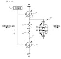
- FIG. 2 is a circuit diagram of the ultrasonic sensor according to the first embodiment of the present invention.
- 2 is a circuit diagram illustrating an internal configuration of a variable band operational amplifier included in the ultrasonic sensor illustrated in FIG. It is a figure showing the operation sequence of an ultrasonic sensor.
- FIG. 2 is a diagram illustrating a signal waveform at each position of the ultrasonic sensor illustrated in FIG. 1.
- 2 is a graph showing gain characteristics before and after a signal amplification frequency band of a low-pass filter formed inside the ultrasonic sensor shown in FIG. 1 is changed.
- 2 is a graph for explaining that high-frequency noise is reduced by a low-pass filter configured inside the ultrasonic sensor illustrated in FIG. 1.
- FIG. 2 is a circuit diagram of an ultrasonic sensor according to a first comparative example, which is compared with the ultrasonic sensor shown in FIG. 1.
- FIG. 4 is a circuit diagram of an ultrasonic sensor according to a second comparative example, which is compared with the ultrasonic sensor shown in FIG. 1. It is a circuit diagram of an ultrasonic sensor according to a second embodiment of the present invention.
- FIG. 10 is a circuit diagram of a drive circuit according to a modified example of the semiconductor switch in the ultrasonic sensor shown in FIG. 9.
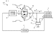
- FIG. 1 is a circuit diagram of an ultrasonic sensor 1A according to the first embodiment of the present invention.
- the ultrasonic sensor 1A is mounted on a vehicle, for example, and is used to measure the distance from itself to an object according to the time from emitting an ultrasonic wave to receiving a reflected wave.
- the ultrasonic sensor 1A includes a piezoelectric element 2, which is a vibrator that emits ultrasonic waves, a transmission circuit 3, a reception circuit 4, a reverberation vibration suppression circuit 5, and a control circuit 6.
- the piezoelectric element 2 has a piezoelectric body 2a that is a vibrating body, a drive electrode 2b, a detection electrode 2c, and a common electrode 2d.
- the common electrode 2d is connected to a reference voltage such as a ground voltage.
- An excitation signal that causes the piezoelectric body 2a to vibrate is applied between the drive electrode 2b and the common electrode 2d. Further, a charge corresponding to the vibration of the piezoelectric body 2a appears between the detection electrode 2c and the common electrode 2d, and the charge is extracted as a detection signal.
- the transmission circuit 3 outputs an excitation signal A for oscillating the piezoelectric body 2a to the drive electrode 2b.
- the receiving circuit 4 inputs a detection signal detected by the detection electrode 2c when the piezoelectric body 2a vibrates by receiving a reflected wave or the like.
- the reverberation signal is input from the detection electrode 2 c to the reception circuit 4, and the reception circuit 4 outputs a reverberation vibration suppression circuit control signal for controlling the reverberation vibration suppression circuit 5 to the reverberation vibration suppression circuit 5 in accordance with the input reverberation signal. I do.
- the reverberation vibration suppression circuit 5 is configured using a variable band operational amplifier 50.
- the reverberation suppression circuit 5 amplifies the reverberation suppression circuit control signal output from the reception circuit 4 after the output of the excitation signal A from the transmission circuit 3 to the drive electrode 2b is stopped, and suppresses the reverberation vibration.
- a control signal is generated and given to the drive electrode 2b.
- the suppression control signal is generated, for example, as a voltage signal whose phase is inverted with respect to the reverberation signal so that the vibration of the piezoelectric body 2a due to the reverberation vibration is canceled.
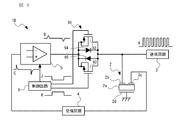
- the variable band operational amplifier 50 has an internal configuration shown in FIG. 2 in which the frequency band of signal amplification is variable.
- FIG. 2A shows an example of a schematic configuration
- FIG. 2B shows an example of a detailed configuration. That is, the band variable operational amplifier 50 includes a voltage-current converter 51 in the input stage, a variable resistor 52 in the intermediate stage, and a current-voltage converter 53 in the output stage.
- the voltage-current converter 51 includes a pair of MOSFETs (MOS field effect transistors) to which respective input voltages of the non-inverting input terminal (+) 50a and the inverting input terminal (-) 50b of the band variable operational amplifier 50 are respectively applied to the gates.
- MOSFETs MOS field effect transistors
- the current-voltage converter 53 includes a MOSFET 53a having a constant voltage Vb applied to the gate to form a constant current source, and a MOSFET 53b connected in series to the MOSFET 53a and having a capacitor 53c connected between the gate and the drain.
- the variable resistance section 52 provided between the voltage-current conversion section 51 and the current-voltage conversion section 53 is composed of a MOSFET 52a having a gate connected to the control circuit 6, and the control circuit 6 varies the resistance value.
- the control circuit 6 controls the resistance value of the variable resistance section 52 after the output of the suppression control signal from the reverberation vibration suppression circuit 5 to the drive electrode 2b is stopped, thereby controlling the frequency of the signal amplification of the band variable operational amplifier 50. Change the band.
- the main pole is formed inside the band variable operational amplifier 50 by the resistance of the variable resistance section 52 and the capacitance formed in the circuit around the variable resistance section 52.
- the control circuit 6 controls the resistance value of the variable resistor section 52 to vary the frequency band of signal amplification by the band variable operational amplifier 50.
- the ultrasonic sensor 1A is generated after the vibration of the piezoelectric body 2a due to reverberation is canceled by the suppression control signal. This high-frequency noise is reduced by changing the frequency of the main pole.
- the current value of the current flowing through the MOSFETs 51e and 53a constituting the constant current source is reduced.
- this current value is reduced, the voltage at each node of the band variable operational amplifier 50 changes, the bias voltage for each MOSFET changes, and the output DC voltage of the band variable operational amplifier 50 changes minutely.
- the voltage at each node does not change. The output of the variable band operational amplifier 50 is not affected.
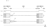
- FIG. 3 shows an operation sequence of the ultrasonic sensor 1A, and time elapses from left to right in the figure.
- the ultrasonic sensor 1A repeats the transmission operation in the period T1, the dereverberation operation in the period T2, and the reception operation in the period T3.
- FIG. 3A is a timing chart of a suppression control signal B output from the reverberation vibration suppression circuit 5 to the drive electrode 2b.
- FIG. 3B is a diagram illustrating a state in which the vibration of the piezoelectric body 2a due to reverberation is suppressed.
- the operation sequence of the ultrasonic sensor 1A when re-excitation does not occur in the piezoelectric body 2a
- FIG. 4C shows the ultrasonic wave when re-excitation occurs in the piezoelectric body 2a after suppressing vibration of the piezoelectric body 2a due to reverberation vibration. It is an operation sequence of the sensor 1A.
- the excitation signal A (see FIG. 4A) is output from the transmission circuit 3 to the drive electrode 2b, and the piezoelectric body 2a is vibrated to generate ultrasonic waves.
- the suppression control signal B (see FIG. 4B) becomes active.
- the generated suppression control signal B is applied to the drive electrode 2b, and the reverberation vibration of the piezoelectric body 2a is suppressed.
- the suppression control signal B has a pulse shape, and a high-frequency noise C (see FIG. 4C) is generated at the rising edge timing and the falling edge timing of the signal. This high-frequency noise C becomes high-frequency noise D attenuated by the band variable operational amplifier 50 (see FIG. 4D).
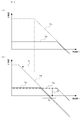
- FIG. 5A shows the frequency of the main pole of the variable band operational amplifier 50, that is, the band before the cutoff frequency of the low-pass filter having the lowest cutoff frequency formed inside the variable band operational amplifier 50 is reduced.
- FIG. 4B is a graph showing the open-loop gain characteristic and the closed-loop gain characteristic of the variable operational amplifier 50.
- FIG. 4B shows the open-loop gain characteristic and the closed-loop gain characteristic of the variable-band operational amplifier 50 when the cutoff frequency is reduced. It is a graph.
- the horizontal axis of each graph is the signal frequency f, and the vertical axis is the gain G of the band variable operational amplifier 50.
- a characteristic line 71a indicated by a dotted line is an open loop gain characteristic of the band variable operational amplifier 50 before the cutoff frequency is reduced, and a characteristic line 72a indicated by a solid line is a closed loop gain characteristic.
- a characteristic line 71b indicated by a dotted line is an open loop gain characteristic of the band variable operational amplifier 50 when the cutoff frequency is lowered, and a characteristic line 72b indicated by a solid line is a closed loop gain characteristic.
- the open-loop gain characteristics and the closed-loop gain characteristics of the band variable operational amplifier 50 are such that the gain G in the frequency band fw where high-frequency noise occurs is indicated by the arrow 74.
- the signal amplification factor of the band variable operational amplifier 50 decreases. Accordingly, as shown in the graph of FIG. 6, the high-frequency noise C is amplified in the closed-loop gain characteristic indicated by the dotted characteristic line 72a of the band variable operational amplifier 50 before the cutoff frequency is reduced.
- the piezoelectric body 2a is not re-excited. Does not occur. Therefore, the vibration generated in the piezoelectric body 2a due to the reception of the reflected wave of the ultrasonic wave in the reception period T3 immediately after the end of the dereverberation period T2 can be detected as the detection wave E by the detection electrode 2c.
- the ultrasonic sensor 11A includes a reverberation vibration suppression circuit 81 including an amplification circuit, a filter, and the like.
- the amplified control signal is switched by a transmission gate 84 composed of an n-channel MOSFET 82 and a p-channel MOSFET 83 to be converted into a suppression control signal, and applied to the drive electrode 2b during the reverberation suppression period T2.
- a drive pulse F that swings to a negative voltage is applied to the gate of the n-channel MOSFET 82
- a drive pulse G that swings to a positive voltage that is the inverted drive pulse F is applied to the gate of the p-channel MOSFET 83.
- the driving voltage of the piezoelectric element 2 is as high as several tens of volts, and a high voltage is required for the suppression control signal for suppressing the reverberation vibration of the piezoelectric body 2a. growing. Further, parasitic capacitances 85 and 86 are generated between the gate and the drain of each of the MOSFETs 82 and 83. The capacitance values of the parasitic capacitances 85 and 86 increase as the element size of the transmission gate 84 increases. Therefore, a high-frequency noise H having a large amplitude is generated at the rising edge timing and the falling edge timing of the suppression control signal applied to the drive electrode 2b. Therefore, when switching from the reverberation suppression period T2 to the reception period T3, the piezoelectric body 2a is re-excited by the high frequency noise H generated at the falling edge of the suppression control signal.
- the transmission gate 84 having a small element size is used, and the amplitudes of the driving pulses F and G applied to the gates of the MOSFETs 82 and 83 are reduced. Further, the parasitic capacitances 85 and 86 generated between the gate and the drain of each of the MOSFETs 82 and 83 also become smaller according to the element size of the transmission gate 84. Therefore, the high-frequency noise H generated at the rising edge timing and the falling edge timing of the suppression control signal applied to the drive electrode 2b has a small amplitude.
- parasitic diodes 87 and 88 are generated between the source and the drain of each of the MOSFETs 82 and 83, and the control signal is amplified at a large magnification in the reverberation vibration suppressing circuit 81. Exceeds directional voltage. Therefore, when switching from the reverberation suppression period T2 to the reception period T3, a signal for exciting the piezoelectric body 2a is output to the drive electrode 2b through the parasitic diodes 87 and 88, and the piezoelectric body 2a is re-excited.
- the ultrasonic sensor 1A according to the present embodiment, as described above, the high-frequency noise C generated when switching from the reverberation suppression period T2 to the reception period T3 is attenuated by reducing the band of the band variable operational amplifier 50. Therefore, the parasitic diodes 87 and 88 do not become conductive, and the piezoelectric body 2a is not re-excited.
- the suppression control signal B is amplified by the band variable operational amplifier 50.
- the reverberation vibration suppression circuit 5 By being provided from the reverberation vibration suppression circuit 5 to the drive electrode 2b, the reverberation vibration of the piezoelectric body 2a is suppressed in the reverberation suppression period T2. Further, in the reception period T3 after the output of the suppression control signal B to the drive electrode 2b is stopped, the signal amplification frequency band of the band variable operational amplifier 50 is changed by the control circuit 6, and inside the band variable operational amplifier 50.
- the signal amplification rate of the band variable operational amplifier 5 in the frequency band of the generated high-frequency noise C is reduced, the signal level of the high-frequency noise D applied to the drive electrode 2b after the reverberation vibration of the piezoelectric body 2a is suppressed. Reduced.
- the frequency of the main pole formed inside the variable band operational amplifier 50 is changed by the control circuit 6, and the frequency of the main pole is reduced, and The signal amplification factor of the band variable operational amplifier 50 in the frequency band of the noise C is reduced. That is, after the output of the suppression control signal B to the drive electrode 2b is stopped, the resistance value of the variable resistance section 52 is changed by the control circuit 6, whereby the capacitance component of the band variable operational amplifier 50 and the variable resistance section 52 are changed. , The signal amplification frequency band of the variable-band operational amplifier 50 is varied with a simple circuit configuration, and the signal amplification factor of the variable-band operational amplifier 50 in the frequency band of the high-frequency noise C decreases. Let me do.
- the high-frequency noise C is reduced by the band variable operational amplifier 50 to a high-frequency noise D at a signal level that does not cause the piezoelectric body 2a to re-vibrate. Therefore, after the reverberation vibration of the piezoelectric body 2a is suppressed, the piezoelectric body 2a is prevented from being re-excited and re-vibrated by the high frequency noise D.
- the reception signal received in the reception period T3 immediately after the reverberation vibration of the piezoelectric body 2a is suppressed is not buried in the noise N caused by the re-vibration of the piezoelectric body 2a, and the reception signal can be correctly received.
- the band variable operational amplifier 50 is easy to manufacture and small in size.
- the ultrasonic sensor 1A is small and manufactured at low cost.
- FIG. 9 is a circuit diagram of an ultrasonic sensor 1B according to the second embodiment of the present invention.
- the ultrasonic sensor 1B includes a semiconductor switch 91 provided between the reverberation vibration suppression circuit 5 and the drive electrode 2b.
- the control circuit 6 controls the semiconductor switch 91 to a conductive state when the reverberation vibration suppression circuit 5 outputs the suppression control signal B, and stops the output of the suppression control signal B from the reverberation vibration suppression circuit 5 to the drive electrode 2b. After that, the semiconductor switch 91 is turned off.
- the ultrasonic sensor 1B according to the second embodiment differs from the ultrasonic sensor 1A according to the first embodiment in these points. The configuration other than these differences is the same as that of the ultrasonic sensor 1A according to the first embodiment.
- the semiconductor switch 91 includes a transmission gate in which the source / drain of the n-channel MOSFET 92 and the source / drain of the p-channel MOSFET 93 are connected in parallel.
- a parasitic diode 94 having a forward direction from the source to the drain is formed between the source and the drain of the MOSFET 92, and a parasitic diode 95 having a forward direction from the drain to the source is formed between the source and the drain of the MOSFET 93.
- the MOSFET 92 is turned on when the drive pulse J is applied to the gate from the control circuit 6, and the MOSFET 93 is turned on when the drive pulse K is applied to the gate from the control circuit 6.
- the semiconductor switch 91 is controlled by the control circuit 6 during the reception period T3 after the output of the suppression control signal B from the reverberation vibration suppression circuit 5 to the drive electrode 2b is stopped. It is controlled to a non-conductive state.
- the signal amplification frequency band of the variable band operational amplifier 50 is varied by the control circuit 6, and the signal amplification factor of the variable band operational amplifier 50 in the frequency band of the high frequency noise C generated inside the variable band operational amplifier 50
- the signal amplification factor is such that the signal level of the high-frequency noise C is reduced below the forward voltage of the parasitic diodes 94 and 95 parasitic on the switch 91, the reception period T3 after the reverberation vibration of the piezoelectric body 2a is suppressed.
- the high-frequency noise D output from the reverberation vibration suppression circuit 5 cannot pass through the parasitic diodes 94 and 95, and is cut off by the semiconductor switch 91.
- the high-frequency noise D has no effect on the drive electrode 2b during the reception period T3 after the reverberation vibration of the piezoelectric body 2a is suppressed, and the piezoelectric body 2a is surely removed. It will not be re-excited by the high frequency noise D, and will not cause re-oscillation.
- FIG. 10 is a circuit diagram showing a modification of the drive circuit of the semiconductor switch 91 in the ultrasonic sensor 1B shown in FIG.
- the same or corresponding parts as those in FIG. 9 are denoted by the same reference numerals, and the description thereof will be omitted.
- the driving circuit of the semiconductor switch 91 includes a first variable current source 10, a first resistor 11, a second resistor 12, and a second variable current source 13 in this order between the positive power supply VDD and the negative power supply VSS. And a connection point 14 between the first resistor 11 and the second resistor 12 is connected to the output line 15 of the reverberation suppression circuit 5.
- the sources of the n-channel MOSFET 92 and the p-channel MOSFET 93 are connected to a connection point 14 between the first resistor 11 and the second resistor 12, and the gate of the n-channel MOSFET 92 is connected to the first variable current source 10 and the first resistor 11
- a connection point 16 between the gate and the gate of the p-channel MOSFET 93 is connected to a connection point 17 between the second resistor 12 and the second variable current source 13.
- the current of the current flowing in the series circuit by the first variable current source 10 and the second variable current source 13 is provided between the gate and source of the n-channel MOSFET 92 in the transmission gate forming the semiconductor switch 91.
- a drive voltage determined by the value and the resistance value of the first resistor 11 is applied with reference to a voltage at a connection point 14 between the first resistor 11 and the second resistor 12.
- the gate and the source of the p-channel MOSFET 93 it is determined by the current value of the current flowing through the series circuit by the first variable current source 10 and the second variable current source 13 and the resistance value of the second resistor 12.
- a drive voltage is applied with reference to a voltage at a node 14 between the first resistor 11 and the second resistor 12.
- connection point 14 between the first resistor 11 and the second resistor 12 is connected to the output line 15 of the reverberation vibration suppression circuit 5, so that the voltage at the connection point 14 between the first resistor 11 and the second resistor 12 Changes according to the output voltage of the reverberation vibration suppression circuit 5.
- the output voltage of the reverberation suppression circuit 5 is set between the gate and source of the n-channel MOSFET 92 and between the gate and source of the p-channel MOSFET 93 in the transmission gate. Is applied, the n-channel MOSFET 92 and the p-channel MOSFET 93 are appropriately driven without being affected by the change in the output voltage of the reverberation vibration suppression circuit 5.
- the drive voltage is controlled by the control circuit 6 changing the current value of the current passed through the series circuit by the first variable current source 10 and the second variable current source 13.
- the conduction state of the semiconductor switch 91 is controlled by the control circuit 6 without being affected by a change in the output voltage of the reverberation vibration suppression circuit 5. Therefore, in the reception period T3 after the output of the suppression control signal B from the reverberation vibration suppression circuit 5 to the drive electrode 2b is stopped, the semiconductor switch 91 is appropriately controlled to the non-conductive state by the control circuit 6, and the piezoelectric body 2a Is more reliably prevented from being re-excited by the high-frequency noise D, so that re-oscillation does not occur.
- the case where the vibrator that generates ultrasonic waves is the piezoelectric element 2 has been described. May be a child. In such a case, the same operation and effect as those of the first and second embodiments can be obtained.
- Ultrasonic sensor 2 Piezoelectric element (vibrator) 2a: Piezoelectric body (vibrating body) 2b ... drive electrode 2c ... detection electrode 2d ... common electrode 3 ... transmission circuit 4 ... reception circuit 5 ... reverberation vibration suppression circuit 50 ... band variable operational amplifier 50a ... non-inverting input terminal (+) 50b: inverted input terminal (-) 50c output terminal 6 control circuit 10 first current source 11 first resistor 12 second resistor 13 second current source 14, 16, 17 connection point 91 semiconductor switch 92 n channel MOSFET 93 ... p-channel MOSFET 94, 95 ... parasitic diode
Abstract
振動体の残響振動が抑圧された直後に受信される受信信号を正しく受信することが可能な超音波センサを提供する。超音波センサ1Aでは、送信回路3から駆動電極2bへの励振信号Aの出力が停止された後、抑圧制御信号Bが帯域可変演算増幅器50によって信号増幅されて残響振動抑圧回路5から駆動電極2bに与えられることで、残響抑圧期間T2において、圧電体2aの残響振動が抑圧される。また、駆動電極2bへの抑圧制御信号Bの出力が停止された後の受信期間T3において、帯域可変演算増幅器50の信号増幅周波数帯域が制御回路6によって可変され、帯域可変演算増幅器50の内部で発生する高周波ノイズCの周波数帯域における帯域可変演算増幅器5の信号増幅率が低下させられることで、圧電体2aの残響振動が抑圧された後に駆動電極2bに印加される高周波ノイズDの信号レベルが低減される。
Description
本発明は、超音波を発する振動体の残響振動を抑圧する残響振動抑圧回路を備える超音波センサに関するものである。
従来、この種の超音波センサとしては、例えば、特許文献1に開示されたものがある。この超音波センサは半導体スイッチを備え、半導体スイッチにより、超音波を発する圧電体に設けられる送信用電極と受信用電極との間の電気的な経路を導通状態と非導通状態とに切り替える。送信用電極への交流電圧印加後に半導体スイッチによって上記経路を導通状態にすることで、圧電体の残響振動に応じて圧電体の受信用領域から出力される残響信号が送信用電極にフィードバックされる。残響信号が電圧として送信用電極にフィードバックされることで、圧電体の残響振動が相殺されて抑圧される。残響信号が送信用電極にフィードバックされた後、上記経路を導通状態から非導通状態に切り替えることで、超音波センサは受信可能状態にされる。
しかしながら、上記従来の超音波センサにおいては、残響信号が電圧として送信用電極にフィードバックされて圧電素子の残響振動が一旦抑制されても、半導体スイッチのスイッチング等によって生じる高周波ノイズにより、圧電体が再励起されて再振動する。このため、半導体スイッチを導通状態から非導通状態に切り替えて超音波センサを受信可能状態にしても、振動体の残響振動が抑圧された直後に受信される受信信号がこの再振動に起因する雑音に埋もれて、受信信号を正しく受信することができない。
本発明はこのような課題を解決するためになされたもので、
振動体に振動を生じさせる励振信号が印加される駆動電極および振動体の振動に応じた検出信号を取り出す検出電極を有する超音波を発する振動子と、
振動体を振動させる励振信号を駆動電極へ出力する送信回路と、
検出電極に検出される検出信号を入力する受信回路と、
送信回路から駆動電極への励振信号の出力が停止された後に受信回路から出力される振動体の残響振動に応じた残響振動抑圧回路制御信号を増幅して残響振動を抑圧する抑圧制御信号を生成し、駆動電極に与える、信号増幅の周波数帯域が可変な帯域可変演算増幅器を有する残響振動抑圧回路と、残響振動抑圧回路から駆動電極への抑圧制御信号の出力が停止された後に帯域可変演算増幅器の信号増幅の周波数帯域を可変させる制御回路とを備え、超音波センサを構成した。
本構成によれば、送信回路から駆動電極への励振信号の出力が停止された後、抑圧制御信号が帯域可変演算増幅器によって信号増幅されて残響振動抑圧回路から駆動電極に与えられることで、振動体の残響振動が抑圧される。また、駆動電極への抑圧制御信号の出力が停止された後、帯域可変演算増幅器の信号増幅周波数帯域が制御回路によって可変され、帯域可変演算増幅器の内部で発生する高周波ノイズの周波数帯域における帯域可変演算増幅器の信号増幅率が低下させられることで、振動体の残響振動が抑圧された後に駆動電極に印加される高周波ノイズの信号レベルが低減される。したがって、振動体の残響振動が抑圧された後、高周波ノイズによって振動体が再励起されて再振動するのが防止される。このため、振動体の残響振動が抑圧された直後に受信が可能になる。
よって、本発明によれば、振動体の残響振動が抑圧された直後に受信される受信信号を正しく受信することが可能な超音波センサを提供することが出来る。
次に、本発明の超音波センサを実施するための形態について、説明する。
図1は、本発明の第1の実施形態による超音波センサ1Aの回路図である。
超音波センサ1Aは、例えば、車両に搭載されて、超音波を発してから反射波を受信するまでの時間に応じて、自身から物体までの距離を計測するのに用いられる。超音波センサ1Aは、超音波を発する振動子である圧電素子2、送信回路3、受信回路4、残響振動抑圧回路5、および制御回路6を備えて構成される。圧電素子2は、振動体である圧電体2a、駆動電極2b、検出電極2cおよび共通電極2dを有する。共通電極2dは接地電圧等の基準電圧に接続される。駆動電極2bおよび共通電極2d間には、圧電体2aに振動を生じさせる励振信号が印加される。また、検出電極2cおよび共通電極2d間には、圧電体2aの振動に応じた電荷が現れ、この電荷が検出信号として取り出される。送信回路3は、圧電体2aを振動させる励振信号Aを駆動電極2bへ出力する。受信回路4は、反射波等の受信によって圧電体2aが振動することで、検出電極2cに検出される検出信号を入力する。
駆動電極2bに励振信号Aが印加されることで、圧電体2aが振動して、気中などに向けて超音波が出射される。この圧電体2aの振動は、送信回路3から駆動電極2bへの励振信号Aの出力が停止された後にも、直ぐには収まらず、しばらく残響振動として継続する。この残響振動により、検出電極2cには残響振動に応じた電圧が残響信号として検出される。受信回路4には検出電極2cからこの残響信号が入力され、受信回路4は、入力した残響信号に応じて残響振動抑圧回路5を制御する残響振動抑圧回路制御信号を残響振動抑圧回路5へ出力する。
残響振動抑圧回路5は帯域可変演算増幅器50を用いて構成される。残響振動抑圧回路5は、送信回路3から駆動電極2bへの励振信号Aの出力が停止された後に受信回路4から出力される残響振動抑圧回路制御信号を増幅して、残響振動を抑圧する抑圧制御信号を生成し、駆動電極2bに与える。抑圧制御信号は、残響振動による圧電体2aの振動が打ち消されるように、例えば、残響信号に対して位相を反転した電圧信号として生成される。
帯域可変演算増幅器50は、信号増幅の周波数帯域が可変な図2に示す内部構成を有し、同図(a)に概略構成、同図(b)に詳細な構成の一例が示される。つまり、帯域可変演算増幅器50は、入力段に電圧電流変換部51、中間段に可変抵抗部52、および出力段に電流電圧変換部53を備える。電圧電流変換部51は、帯域可変演算増幅器50の非反転入力端子(+)50aおよび反転入力端子(-)50bの各入力電圧がゲートにそれぞれ印加される一対のMOSFET(MOS型電界効果トランジスタ)51a、51b、カレントミラー回路を構成する一対のMOSFET51c、51d、およびゲートに一定の電圧Vbが与えられて定電流源を構成するMOSFET51eから構成され、非反転入力端子(+)50aおよび反転入力端子(-)50b間に入力される差電圧を電流に変換する。電流電圧変換部53は、ゲートに一定の電圧Vbが与えられて定電流源を構成するMOSFET53a、および、MOSFET53aに直列に接続されて、ゲート・ドレイン間にコンデンサ53cが接続されるMOSFET53bから構成され、電圧電流変換部51によって変換される電流を電圧に変換して、帯域可変演算増幅器50の出力端子50cへ出力する。なお、図2(b)に示す内部回路は一例であり、電圧電流変換部51および電流電圧変換部53の構成はこれに限定されない。
電圧電流変換部51および電流電圧変換部53間に設けられる可変抵抗部52は、ゲートに制御回路6が接続されたMOSFET52aから構成され、制御回路6によって抵抗値が可変される。制御回路6は、残響振動抑圧回路5から駆動電極2bへの抑圧制御信号の出力が停止された後に、可変抵抗部52の抵抗値を制御することで、帯域可変演算増幅器50の信号増幅の周波数帯域を可変させる。本実施形態では、可変抵抗部52の抵抗とその周囲の回路に形成される容量とにより、帯域可変演算増幅器50の内部に主要極を構成する。制御回路6は、可変抵抗部52の抵抗値を制御して、帯域可変演算増幅器50による信号増幅の周波数帯域を可変する。
帯域可変演算増幅器50の内部には、各MOSFETのスイッチングにより高周波ノイズが発生するが、本実施形態による超音波センサ1Aは、残響振動による圧電体2aの振動が抑圧制御信号で打ち消された後に生じるこの高周波ノイズを、主要極の周波数を変化させることで、低減する。
帯域可変演算増幅器50の信号増幅周波数帯域を可変するには、一般的に、定電流源を構成するMOSFET51e、53aによって流される電流の電流値を低下させることで行われる。しかし、この電流値を低下させると、帯域可変演算増幅器50の各ノードにおける電圧が変化し、各MOSFETに対するバイアス電圧が変化して、帯域可変演算増幅器50の出力DC電圧が微小に変化する。これに対して、上記のように、主要極の周波数を変化させることで、帯域可変演算増幅器50による信号増幅周波数帯域を可変する本実施形態においては、各ノードにおける電圧が変化することはなく、帯域可変演算増幅器50の出力に影響を与えることはない。
図3は、超音波センサ1Aの動作シーケンスを示し、図の左から右へ時間が経過する。超音波センサ1Aは、期間T1における送信動作、期間T2における残響抑圧動作、期間T3における受信動作を繰り返す。同図(a)は、残響振動抑圧回路5から駆動電極2bへ出力される抑圧制御信号Bのタイミングチャート、同図(b)は、残響振動による圧電体2aの振動を抑圧した後、圧電体2aに再励起が生じないときにおける超音波センサ1Aの動作シーケンス、同図(c)は、残響振動による圧電体2aの振動を抑圧した後、圧電体2aに再励起が生じたときにおける超音波センサ1Aの動作シーケンスである。
送信期間T1においては、送信回路3から駆動電極2bへ励振信号A(図4(a)参照)が出力され、圧電体2aが振動させられて超音波が発生する。送信回路3から駆動電極2bへの励振信号Aの出力が停止された後の残響抑圧期間T2では、抑圧制御信号B(図4(b)参照)がアクティブになる。生成された抑圧制御信号Bは駆動電極2bに印加され、圧電体2aの残響振動が抑圧される。抑圧制御信号Bはパルス状をしており、その信号の立ち上がりエッジタイミングおよび立ち下がりエッジタイミングに高周波ノイズC(図4(c)参照)が発生する。この高周波ノイズCは、帯域可変演算増幅器50により減衰した高周波ノイズD(図4(d)参照)となる。
図5(a)は、帯域可変演算増幅器50の主要極の周波数、すなわち、帯域可変演算増幅器50の内部に構成されるカットオフ周波数の一番低いローパスフィルタのカットオフ周波数が引き下げられる前における帯域可変演算増幅器50の開ループ利得特性および閉ループ利得特性を表すグラフ、同図(b)は、このカットオフ周波数が引き下げられたときにおける帯域可変演算増幅器50の開ループ利得特性および閉ループ利得特性を表すグラフである。各グラフの横軸は信号周波数f、縦軸は帯域可変演算増幅器50の利得Gである。また、同図(a)において点線で示す特性線71aはカットオフ周波数が引き下げられる前における帯域可変演算増幅器50の開ループ利得特性、実線で示す特性線72aは閉ループ利得特性である。また、同図(b)において点線で示す特性線71bはカットオフ周波数が引き下げられたときにおける帯域可変演算増幅器50の開ループ利得特性、実線で示す特性線72bは閉ループ利得特性である。
矢印73に示されるようにカットオフ周波数が引き下げられると、帯域可変演算増幅器50の開ループ利得特性および閉ループ利得特性は、高周波ノイズが発生する周波数帯域fwにおける利得Gが矢印74に示されるように低下して、帯域可変演算増幅器50の信号増幅率が小さくなる。したがって、図6に示すグラフのように、高周波ノイズCは、カットオフ周波数が引き下げられる前における帯域可変演算増幅器50の点線の特性線72aで示される閉ループ利得特性では、信号増幅されてしまうが、カットオフ周波数が引き下げられたときにおける帯域可変演算増幅器50の実線の特性線72bで示される閉ループ利得特性では、信号増幅率が小さく、矢印75に示されるように振幅が減衰した高周波ノイズDに低減される。なお、図6に示すグラフの縦軸および横軸は図5に示す各グラフと同じである。
したがって、図3(b)に示す動作シーケンスの受信期間T3において、圧電体2aの残響振動が抑圧された後には、高周波ノイズCが高周波ノイズDに低減されるので、圧電体2aに再励起は生じない。このため、残響抑圧期間T2が終了した直後の受信期間T3に、超音波の反射波が受信されることで圧電体2aに生じる振動は、検出電極2cに検出波Eとして捉えることができる。しかし、図3(c)に示す動作シーケンスの受信期間T3において、圧電体2aの残響振動が抑圧された後に、帯域可変演算増幅器50から高周波ノイズCが駆動電極2bに出力されると、圧電体2aに再励起が生じる。したがって、残響抑圧期間T2が終了した直後の受信期間T3に、圧電体2aの再励起による振動によって雑音Nが生じる。このため、残響抑圧期間T2が終了した直後の受信期間T3に反射波が受信されると、その反射波は雑音Nに埋もれて検出することができない。この結果、超音波センサ1Aは近距離の物体を検出できなくなる。
上記のように、残響抑圧期間T2から受信期間T3への切り替えで、抑圧制御信号Bの立ち下がりエッジに起因にして高周波ノイズCが生じ、この高周波ノイズCが圧電体2aに再励起を引き起こす。このような高周波ノイズに起因する圧電体2aの再励起は、図7に第1の比較例として示す超音波センサ11Aにおいても生じる。なお、図7において図1と同一または相当する部分には同一符号を付してその説明は省略する。
超音波センサ11Aは、増幅回路およびフィルタ等から構成される残響振動抑圧回路81を備え、受信回路4から出力される制御信号を残響振動抑圧回路81で増幅する。増幅された制御信号は、nチャネルMOSFET82およびpチャネルMOSFET83からなるトランスミッションゲート84でスイッチングされて抑圧制御信号に変換され、残響抑圧期間T2において駆動電極2bに与えられる。この際、nチャネルMOSFET82のゲートには負電圧に振れる駆動パルスF、pチャネルMOSFET83のゲートには駆動パルスFが反転した正電圧に振れる駆動パルスGが与えられる。圧電素子2の駆動電圧は数十Vと高く、圧電体2aの残響振動を抑圧する抑圧制御信号も高い電圧が必要となり、トランスミッションゲート84の素子サイズが大きくなって駆動パルスF、Gの振幅も大きくなる。また、各MOSFET82、83のゲート・ドレイン間には寄生容量85、86が生じる。この寄生容量85、86は、トランスミッションゲート84の素子サイズの大きさに伴って容量値も大きくなる。したがって、駆動電極2bに与えられる抑圧制御信号の立ち上がりエッジタイミングおよび立ち下がりエッジタイミングには、振幅の大きな高周波ノイズHが発生する。このため、残響抑圧期間T2から受信期間T3に切り替わる際、抑圧制御信号の立ち下がりエッジに生じる高周波ノイズHによって圧電体2aが再励起されてしまう。
また、高周波ノイズに起因する圧電体2aの再励起は、図8に第2の比較例として示す超音波センサ11Bにおいても生じる。なお、図8において図7と同一または相当する部分には同一符号を付してその説明は省略する。
超音波センサ11Bでは素子サイズの小さなトランスミッションゲート84が使用され、各MOSFET82、83のゲートに与えられる駆動パルスF、Gの振幅は小さくなる。また、各MOSFET82、83のゲート・ドレイン間に生じる寄生容量85、86もトランスミッションゲート84の素子サイズに応じて小さくなる。このため、駆動電極2bに与えられる抑圧制御信号の立ち上がりエッジタイミングおよび立ち下がりエッジタイミングに発生する高周波ノイズHは、振幅が小さくなる。しかし、各MOSFET82、83のソース・ドレイン間に寄生ダイオード87、88が生じ、制御信号が残響振動抑圧回路81で大きな倍率で増幅されるため、高周波ノイズHの電圧が寄生ダイオード87、88の順方向電圧を超える。このため、残響抑圧期間T2から受信期間T3に切り替わる際、寄生ダイオード87、88を通って圧電体2aを励起させる信号が駆動電極2bに出力され、圧電体2aが再励起されてしまう。
しかし、本実施形態による超音波センサ1Aによれば、上記のように、残響抑圧期間T2から受信期間T3に切り替わる際に発生する高周波ノイズCは、帯域可変演算増幅器50の帯域が引き下げられて減衰するので、寄生ダイオード87、88が導通状態にならず、圧電体2aに再励起は生じない。
このような本実施形態による超音波センサ1Aによれば、送信回路3から駆動電極2bへの励振信号Aの出力が停止された後、抑圧制御信号Bが帯域可変演算増幅器50によって信号増幅されて残響振動抑圧回路5から駆動電極2bに与えられることで、残響抑圧期間T2において、圧電体2aの残響振動が抑圧される。また、駆動電極2bへの抑圧制御信号Bの出力が停止された後の受信期間T3において、帯域可変演算増幅器50の信号増幅周波数帯域が制御回路6によって可変され、帯域可変演算増幅器50の内部で発生する高周波ノイズCの周波数帯域における帯域可変演算増幅器5の信号増幅率が低下させられることで、圧電体2aの残響振動が抑圧された後に駆動電極2bに印加される高周波ノイズDの信号レベルが低減される。
本実施形態では、帯域可変演算増幅器50の信号増幅周波数帯域は、帯域可変演算増幅器50の内部に構成される主要極の周波数が制御回路6によって可変され、主要極の周波数が引き下げられて、高周波ノイズCの周波数帯域における帯域可変演算増幅器50の信号増幅率が低下させられる。つまり、駆動電極2bへの抑圧制御信号Bの出力が停止された後、制御回路6によって可変抵抗部52の抵抗値が可変されることで、帯域可変演算増幅器50の容量成分と可変抵抗部52から構成されるローパスフィルタの時定数が変わり、帯域可変演算増幅器50の信号増幅周波数帯域が簡単な回路構成で可変されて、高周波ノイズCの周波数帯域における帯域可変演算増幅器50の信号増幅率が低下させられる。
したがって、圧電体2aの残響振動が抑圧された後、高周波ノイズCは、帯域可変演算増幅器50によって圧電体2aに再振動を起こさない信号レベルの高周波ノイズDに低減される。したがって、圧電体2aの残響振動が抑圧された後、高周波ノイズDによって圧電体2aが再励起されて再振動するのが防止される。このため、圧電体2aの残響振動が抑圧された直後の受信期間T3に受信される受信信号が圧電体2aの再振動に起因する雑音Nに埋もれなくなり、受信信号を正しく受信することが可能になる。
また、本実施形態による超音波センサ1Aによれば、可変抵抗部52が電圧電流変換部51および電流電圧変換部53と共にMOSFETから構成されることで、帯域可変演算増幅器50は製造容易でかつ小型に構成され、超音波センサ1Aは小型で安価に製造される。
図9は、本発明の第2の実施形態による超音波センサ1Bの回路図である。
超音波センサ1Bは、残響振動抑圧回路5と駆動電極2bとの間に設けられる半導体スイッチ91を備える。制御回路6は、残響振動抑圧回路5から抑圧制御信号Bが出力される際に半導体スイッチ91を導通状態に制御し、残響振動抑圧回路5から駆動電極2bへの抑圧制御信号Bの出力が停止された後に半導体スイッチ91を非導通状態に制御する。第2の実施形態による超音波センサ1Bは、これらの点が第1の実施形態による超音波センサ1Aと相違する。これらの相違点以外の構成は第1の実施形態による超音波センサ1Aと同様である。
半導体スイッチ91は、nチャネルMOSFET92のソース・ドレイン間とpチャネルMOSFET93のソース・ドレイン間とが並列に接続されたトランスミッションゲートから構成される。MOSFET92のソース・ドレイン間にはソースからドレインを順方向とする寄生ダイオード94、MOSFET93のソース・ドレイン間にはドレインからソースを順方向とする寄生ダイオード95が生じる。MOSFET92は制御回路6からゲートに駆動バルスJが印加されることで導通状態になり、MOSFET93は制御回路6からゲートに駆動バルスKが印加されることで導通状態になる。
本実施形態による超音波センサ1Bによれば、上記の第1の実施形態による超音波センサ1Aと同様な作用効果が奏される。さらに、本実施形態による超音波センサ1Bによれば、残響振動抑圧回路5から駆動電極2bへの抑圧制御信号Bの出力が停止された後の受信期間T3に、半導体スイッチ91が制御回路6によって非導通状態に制御される。この際、帯域可変演算増幅器50の信号増幅周波数帯域が制御回路6によって可変され、帯域可変演算増幅器50の内部で発生する高周波ノイズCの周波数帯域における帯域可変演算増幅器50の信号増幅率が、半導体スイッチ91に寄生する寄生ダイオード94、95の順方向電圧以下に高周波ノイズCの信号レベルを低下させる信号増幅率になっていると、圧電体2aの残響振動が抑圧された後の受信期間T3に残響振動抑圧回路5から出力される高周波ノイズDは寄生ダイオード94、95を通ることができずに、半導体スイッチ91によって遮断される。したがって、本実施形態による超音波センサ1Bによれば、圧電体2aの残響振動が抑圧された後の受信期間T3に高周波ノイズDは駆動電極2bに何ら影響を与えなくなり、圧電体2aは確実に高周波ノイズDによって再励起されなくなり、再振動を起こさなくなる。
図10は、図9に示す超音波センサ1Bにおける半導体スイッチ91の駆動回路の変形例を示す回路図である。図10において図9と同一または相当する部分には同一符号を付してその説明は省略する。
この変形例による半導体スイッチ91の駆動回路は、第1の可変電流源10、第1の抵抗11、第2の抵抗12、第2の可変電流源13がこの順に正電源VDDおよび負電源VSS間に直列接続され、第1の抵抗11および第2の抵抗12間の接続点14が残響振動抑圧回路5の出力線15に接続される直列回路を備えている。nチャネルMOSFET92およびpチャネルMOSFET93の各ソースは第1の抵抗11および第2の抵抗12間の接続点14に接続され、nチャネルMOSFET92のゲートは第1の可変電流源10および第1の抵抗11間の接続点16、pチャネルMOSFET93のゲートは第2の抵抗12および第2の可変電流源13間の接続点17に接続される。
本構成によれば、半導体スイッチ91を構成するトランスミッションゲートにおけるnチャネルMOSFET92のゲート・ソース間には、第1の可変電流源10および第2の可変電流源13によって直列回路に流される電流の電流値と第1の抵抗11の抵抗値とによって定まる駆動電圧が、第1の抵抗11および第2の抵抗12間の接続点14の電圧を基準にして印加される。また、pチャネルMOSFET93のゲート・ソース間には、第1の可変電流源10および第2の可変電流源13によって直列回路に流される電流の電流値と第2の抵抗12の抵抗値とによって定まる駆動電圧が、第1の抵抗11および第2の抵抗12間の接続点14の電圧を基準にして印加される。第1の抵抗11および第2の抵抗12間の接続点14は残響振動抑圧回路5の出力線15に接続されるので、第1の抵抗11および第2の抵抗12間の接続点14の電圧は、残響振動抑圧回路5の出力電圧にしたがって変化する。
しかし、残響振動抑圧回路5の出力電圧が変化しても、トランスミッションゲートにおけるnチャネルMOSFET92のゲート・ソース間、およびpチャネルMOSFET93のゲート・ソース間には、残響振動抑圧回路5の出力電圧を基準とする上記の各駆動電圧が印加されるので、nチャネルMOSFET92およびpチャネルMOSFET93は、残響振動抑圧回路5の出力電圧の変化に影響を受けずに適切に駆動される。また、この駆動電圧は、第1の可変電流源10および第2の可変電流源13によって直列回路に流される電流の電流値が制御回路6によって可変されることで制御される。このため、半導体スイッチ91は、残響振動抑圧回路5の出力電圧の変化に影響を受けずに、その導通状態が制御回路6によって制御される。よって、残響振動抑圧回路5から駆動電極2bへの抑圧制御信号Bの出力が停止された後の受信期間T3において、半導体スイッチ91は制御回路6によって適切に非導通状態に制御され、圧電体2aはより確実に高周波ノイズDによって再励起されなくなり、再振動を起こさなくなる。
なお、第1の実施形態による超音波センサ1A並びに第2の実施形態による超音波センサ1Bでは、超音波を発生する振動子が圧電素子2である場合について説明したが、静電容量型の振動子であってもよい。その場合においても第1および第2の各実施形態と同様な作用効果が奏される。
1A、1B…超音波センサ
2…圧電素子(振動子)
2a…圧電体(振動体)
2b…駆動電極
2c…検出電極
2d…共通電極
3…送信回路
4…受信回路
5…残響振動抑圧回路
50…帯域可変演算増幅器
50a…非反転入力端子(+)
50b…反転入力端子(-)
50c…出力端子
6…制御回路
10…第1の電流源
11…第1の抵抗
12…第2の抵抗
13…第2の電流源
14、16、17…接続点
91…半導体スイッチ
92…nチャネルMOSFET
93…pチャネルMOSFET
94、95…寄生ダイオード
2…圧電素子(振動子)
2a…圧電体(振動体)
2b…駆動電極
2c…検出電極
2d…共通電極
3…送信回路
4…受信回路
5…残響振動抑圧回路
50…帯域可変演算増幅器
50a…非反転入力端子(+)
50b…反転入力端子(-)
50c…出力端子
6…制御回路
10…第1の電流源
11…第1の抵抗
12…第2の抵抗
13…第2の電流源
14、16、17…接続点
91…半導体スイッチ
92…nチャネルMOSFET
93…pチャネルMOSFET
94、95…寄生ダイオード
Claims (6)
- 振動体に振動を生じさせる励振信号が印加される駆動電極および前記振動体の振動に応じた検出信号を取り出す検出電極を有する超音波を発する振動子と、
前記振動体を振動させる前記励振信号を前記駆動電極へ出力する送信回路と、
前記検出電極に検出される前記検出信号を入力する受信回路と、
前記送信回路から前記駆動電極への前記励振信号の出力が停止された後に前記受信回路から出力される前記振動体の残響振動に応じた残響振動抑圧回路制御信号を増幅して前記残響振動を抑圧する抑圧制御信号を生成し、前記駆動電極に与える、信号増幅の周波数帯域が可変な帯域可変演算増幅器を有する残響振動抑圧回路と、
前記残響振動抑圧回路から前記駆動電極への前記抑圧制御信号の出力が停止された後に前記帯域可変演算増幅器の信号増幅の周波数帯域を可変させる制御回路と
を備える超音波センサ。 - 前記制御回路は、前記帯域可変演算増幅器の主要極の周波数を変化させることで信号増幅の周波数帯域を可変することを特徴とする請求項1に記載の超音波センサ。
- 前記残響振動抑圧回路と前記駆動電極との間に設けられる半導体スイッチを備え、
前記制御回路は前記半導体スイッチの導通状態を制御する
ことを特徴とする請求項1または請求項2に記載の超音波センサ。 - 前記帯域可変演算増幅器は、入力される差電圧を電流に変換する電圧電流変換部と、前記電圧電流変換部によって変換される電流を電圧に変換する電流電圧変換部と、前記電圧電流変換部と前記電流電圧変換部の間に設けられる、前記制御回路によって抵抗値が可変される可変抵抗部とを備えることを特徴とする請求項1から請求項3のいずれか1項に記載の超音波センサ。
- 前記可変抵抗部はMOSFETで構成されることを特徴とする請求項4に記載の超音波センサ。
- 第1の可変電流源、第1の抵抗、第2の抵抗、第2の可変電流源がこの順に正電源および負電源間に直列接続され、前記第1の抵抗および前記第2の抵抗間の接続点が前記残響振動抑圧回路の出力に接続される直列回路を備え、
前記半導体スイッチは、nチャネルMOSFETのソース・ドレイン間とpチャネルMOSFETのソース・ドレイン間とが並列に接続されたトランスミッションゲートから構成され、前記nチャネルMOSFETおよび前記pチャネルMOSFETの各ソースが前記第1の抵抗および前記第2の抵抗間の接続点、前記nチャネルMOSFETのゲートが前記第1の可変電流源および前記第1の抵抗間の接続点、前記pチャネルMOSFETのゲートが前記第2の抵抗および前記第2の可変電流源間の接続点に接続される
ことを特徴とする請求項3または請求項3を引用する請求項4または請求項3を引用する請求項4に従属する請求項5に記載の超音波センサ。
Priority Applications (2)
| Application Number | Priority Date | Filing Date | Title |
|---|---|---|---|
| JP2020528775A JP6981549B2 (ja) | 2018-07-06 | 2019-06-18 | 超音波センサ |
| US17/130,341 US20210107030A1 (en) | 2018-07-06 | 2020-12-22 | Ultrasonic sensor |
Applications Claiming Priority (2)
| Application Number | Priority Date | Filing Date | Title |
|---|---|---|---|
| JP2018129396 | 2018-07-06 | ||
| JP2018-129396 | 2018-07-06 |
Related Child Applications (1)
| Application Number | Title | Priority Date | Filing Date |
|---|---|---|---|
| US17/130,341 Continuation US20210107030A1 (en) | 2018-07-06 | 2020-12-22 | Ultrasonic sensor |
Publications (1)
| Publication Number | Publication Date |
|---|---|
| WO2020008868A1 true WO2020008868A1 (ja) | 2020-01-09 |
Family
ID=69060250
Family Applications (1)
| Application Number | Title | Priority Date | Filing Date |
|---|---|---|---|
| PCT/JP2019/024172 WO2020008868A1 (ja) | 2018-07-06 | 2019-06-18 | 超音波センサ |
Country Status (3)
| Country | Link |
|---|---|
| US (1) | US20210107030A1 (ja) |
| JP (1) | JP6981549B2 (ja) |
| WO (1) | WO2020008868A1 (ja) |
Cited By (1)
| Publication number | Priority date | Publication date | Assignee | Title |
|---|---|---|---|---|
| WO2022201681A1 (ja) * | 2021-03-23 | 2022-09-29 | ローム株式会社 | 半導体装置及び超音波センサ |
Families Citing this family (1)
| Publication number | Priority date | Publication date | Assignee | Title |
|---|---|---|---|---|
| CN116930800B (zh) * | 2023-09-18 | 2023-12-19 | 湖南恩智测控技术有限公司 | 燃料电池阻抗测量装置及方法 |
Citations (5)
| Publication number | Priority date | Publication date | Assignee | Title |
|---|---|---|---|---|
| JPH03282386A (ja) * | 1990-03-30 | 1991-12-12 | Yokogawa Electric Corp | 超音波距離計 |
| JP2012065308A (ja) * | 2010-09-17 | 2012-03-29 | Tung Thih Electronic Co Ltd | 制御装置 |
| JP2015190817A (ja) * | 2014-03-28 | 2015-11-02 | パナソニックIpマネジメント株式会社 | 超音波センサ |
| WO2016167003A1 (ja) * | 2015-04-13 | 2016-10-20 | 株式会社村田製作所 | 超音波センサ、および、その制御方法 |
| JP2017172989A (ja) * | 2016-03-18 | 2017-09-28 | 株式会社Soken | 物体検知装置 |
Family Cites Families (5)
| Publication number | Priority date | Publication date | Assignee | Title |
|---|---|---|---|---|
| US6169765B1 (en) * | 1997-05-28 | 2001-01-02 | Integration Associates, Inc. | Apparatus and method for output signal pulse width error correction in a communications receiver |
| JP4499877B2 (ja) * | 2000-06-13 | 2010-07-07 | セイコーインスツル株式会社 | 超音波モータおよび超音波モータ付き電子機器 |
| JP5671429B2 (ja) * | 2011-08-26 | 2015-02-18 | ルネサスエレクトロニクス株式会社 | 半導体装置 |
| CN104823072B (zh) * | 2014-04-11 | 2017-07-28 | 深圳市大疆创新科技有限公司 | 距离传感系统及方法 |
| US9954485B2 (en) * | 2016-05-09 | 2018-04-24 | Nxp Usa, Inc. | Amplitude detection with compensation |
-
2019
- 2019-06-18 WO PCT/JP2019/024172 patent/WO2020008868A1/ja active Application Filing
- 2019-06-18 JP JP2020528775A patent/JP6981549B2/ja active Active
-
2020
- 2020-12-22 US US17/130,341 patent/US20210107030A1/en active Pending
Patent Citations (5)
| Publication number | Priority date | Publication date | Assignee | Title |
|---|---|---|---|---|
| JPH03282386A (ja) * | 1990-03-30 | 1991-12-12 | Yokogawa Electric Corp | 超音波距離計 |
| JP2012065308A (ja) * | 2010-09-17 | 2012-03-29 | Tung Thih Electronic Co Ltd | 制御装置 |
| JP2015190817A (ja) * | 2014-03-28 | 2015-11-02 | パナソニックIpマネジメント株式会社 | 超音波センサ |
| WO2016167003A1 (ja) * | 2015-04-13 | 2016-10-20 | 株式会社村田製作所 | 超音波センサ、および、その制御方法 |
| JP2017172989A (ja) * | 2016-03-18 | 2017-09-28 | 株式会社Soken | 物体検知装置 |
Cited By (1)
| Publication number | Priority date | Publication date | Assignee | Title |
|---|---|---|---|---|
| WO2022201681A1 (ja) * | 2021-03-23 | 2022-09-29 | ローム株式会社 | 半導体装置及び超音波センサ |
Also Published As
| Publication number | Publication date |
|---|---|
| JPWO2020008868A1 (ja) | 2021-05-13 |
| US20210107030A1 (en) | 2021-04-15 |
| JP6981549B2 (ja) | 2021-12-15 |
Similar Documents
| Publication | Publication Date | Title |
|---|---|---|
| JP4310339B2 (ja) | 発振出力のリークを防止可能とするレーダ用発振器 | |
| KR101118865B1 (ko) | D급 증폭기 | |
| WO2020008868A1 (ja) | 超音波センサ | |
| GB2188208A (en) | Hearing aid amplifier | |
| JP7000550B2 (ja) | 低電力水晶発振器 | |
| JPH06232648A (ja) | 出力回路 | |
| WO2011102062A1 (ja) | 振動型慣性力センサ | |
| KR100496883B1 (ko) | 전류 제어 피더블유엠 회로 및 이를 포함하는 클래스 디이앰프 | |
| JP5806076B2 (ja) | Rfパルス信号生成用スイッチング回路、rfパルス信号生成回路、および物標探知装置 | |
| US11211545B2 (en) | Vibration controller | |
| US20060001488A1 (en) | Digital audio amplifier including phase lead-lag compensator for increasing self-oscillation frequency | |
| JP2015171084A (ja) | 圧電振動子駆動回路 | |
| US20100164590A1 (en) | Semiconductor integrated circuit | |
| US8044735B2 (en) | Oscillator circuit and method for influencing, controlling, or regulating the frequency of an oscillator | |
| EP2960624B1 (en) | Current-to-voltage conversion circuit and self-oscillation circuit | |
| JP2019012955A (ja) | 超音波センサ駆動回路 | |
| JP4042246B2 (ja) | 圧電発振器 | |
| JP6237532B2 (ja) | 自励発振回路 | |
| JP6709497B2 (ja) | 自励発振回路 | |
| JP6220618B2 (ja) | 共振回路及び発振回路 | |
| US9742417B1 (en) | Self-oscillation circuit | |
| JPH04313369A (ja) | 超音波アクチュエータ駆動回路 | |
| EP3205979B1 (en) | Self-oscillation circuit | |
| JP5344955B2 (ja) | 固体振動子発振回路およびこれを用いた物理量センサ | |
| JP4222389B2 (ja) | リンギング低減回路および該リンギング低減回路を備えた半導体集積回路 |
Legal Events
| Date | Code | Title | Description |
|---|---|---|---|
| 121 | Ep: the epo has been informed by wipo that ep was designated in this application |
Ref document number: 19829972 Country of ref document: EP Kind code of ref document: A1 |
|
| ENP | Entry into the national phase |
Ref document number: 2020528775 Country of ref document: JP Kind code of ref document: A |
|
| NENP | Non-entry into the national phase |
Ref country code: DE |
|
| 122 | Ep: pct application non-entry in european phase |
Ref document number: 19829972 Country of ref document: EP Kind code of ref document: A1 |