WO2022196676A1 - 端子、端子付き電線、及び端子の製造方法 - Google Patents
端子、端子付き電線、及び端子の製造方法 Download PDFInfo
- Publication number
- WO2022196676A1 WO2022196676A1 PCT/JP2022/011541 JP2022011541W WO2022196676A1 WO 2022196676 A1 WO2022196676 A1 WO 2022196676A1 JP 2022011541 W JP2022011541 W JP 2022011541W WO 2022196676 A1 WO2022196676 A1 WO 2022196676A1
- Authority
- WO
- WIPO (PCT)
- Prior art keywords
- layer
- terminal
- indium
- imc
- nickel
- Prior art date
- Legal status (The legal status is an assumption and is not a legal conclusion. Google has not performed a legal analysis and makes no representation as to the accuracy of the status listed.)
- Ceased
Links
Images







Classifications
-
- C—CHEMISTRY; METALLURGY
- C23—COATING METALLIC MATERIAL; COATING MATERIAL WITH METALLIC MATERIAL; CHEMICAL SURFACE TREATMENT; DIFFUSION TREATMENT OF METALLIC MATERIAL; COATING BY VACUUM EVAPORATION, BY SPUTTERING, BY ION IMPLANTATION OR BY CHEMICAL VAPOUR DEPOSITION, IN GENERAL; INHIBITING CORROSION OF METALLIC MATERIAL OR INCRUSTATION IN GENERAL
- C23C—COATING METALLIC MATERIAL; COATING MATERIAL WITH METALLIC MATERIAL; SURFACE TREATMENT OF METALLIC MATERIAL BY DIFFUSION INTO THE SURFACE, BY CHEMICAL CONVERSION OR SUBSTITUTION; COATING BY VACUUM EVAPORATION, BY SPUTTERING, BY ION IMPLANTATION OR BY CHEMICAL VAPOUR DEPOSITION, IN GENERAL
- C23C24/00—Coating starting from inorganic powder
- C23C24/08—Coating starting from inorganic powder by application of heat or pressure and heat
-
- H—ELECTRICITY
- H01—ELECTRIC ELEMENTS
- H01R—ELECTRICALLY-CONDUCTIVE CONNECTIONS; STRUCTURAL ASSOCIATIONS OF A PLURALITY OF MUTUALLY-INSULATED ELECTRICAL CONNECTING ELEMENTS; COUPLING DEVICES; CURRENT COLLECTORS
- H01R13/00—Details of coupling devices of the kinds covered by groups H01R12/70 or H01R24/00 - H01R33/00
- H01R13/02—Contact members
- H01R13/03—Contact members characterised by the material, e.g. plating, or coating materials
-
- H—ELECTRICITY
- H01—ELECTRIC ELEMENTS
- H01R—ELECTRICALLY-CONDUCTIVE CONNECTIONS; STRUCTURAL ASSOCIATIONS OF A PLURALITY OF MUTUALLY-INSULATED ELECTRICAL CONNECTING ELEMENTS; COUPLING DEVICES; CURRENT COLLECTORS
- H01R43/00—Apparatus or processes specially adapted for manufacturing, assembling, maintaining, or repairing of line connectors or current collectors or for joining electric conductors
- H01R43/16—Apparatus or processes specially adapted for manufacturing, assembling, maintaining, or repairing of line connectors or current collectors or for joining electric conductors for manufacturing contact members, e.g. by punching and by bending
Definitions
- the present disclosure relates to a terminal, an electric wire with a terminal, and a method for manufacturing the terminal.
- This application claims priority based on Japanese Patent Application No. 2021-046404 dated March 19, 2021, and incorporates all the descriptions described in the Japanese application.
- Patent Document 1 discloses a connection terminal including a copper or copper alloy base material and a plurality of coating layers formed on the surface of the base material.
- the multiple coating layers include, in order from the surface of the base material, an underlying plating layer, a hard plating layer, and a surface plating layer.
- the underlying plating layer is made of nickel or a nickel alloy.
- the hard plating layer is composed of an intermetallic compound containing copper and indium.
- the surface plating layer is composed of indium or an indium alloy.
- the surface plating layer is a layer arranged on the outermost surface of the terminal.
- the surface plating layer containing indium has the effect of reducing the coefficient of friction between the indium-plated terminal and the mating terminal, and the effect of reducing the contact resistance between the indium-plated terminal and the mating terminal.
- the melting point of indium is low, there is a problem that the surface plating layer containing indium is inferior in heat resistance.
- this surface plated layer is exposed to a high-temperature environment approaching the melting point of indium, copper or the like contained in the base material diffuses into the surface plated layer to form an intermetallic compound.
- the contact resistance of the terminal increases.
- the underlying plating layer prevents copper contained in the base material from diffusing into the surface plating layer.
- the hard plating layer suppresses diffusion of nickel or the like contained in the base plating layer into the surface plating layer.
- the terminals of the present disclosure are A terminal-shaped base material made of copper or a copper alloy; a nickel layer disposed on at least part of the surface of the base material; an IMC layer disposed on at least a portion directly above the nickel layer; an indium layer disposed immediately above the IMC layer;
- the IMC layer is composed of an intermetallic compound containing nickel and indium,
- the IMC layer has an average thickness of 0.13 ⁇ m or more.
- the electric wire with terminal of the present disclosure is an electric wire; and a terminal attached to the end of the electric wire, The terminal is the terminal of the present disclosure.
- a method for manufacturing a terminal of the present disclosure includes: A step of preparing a base material composed of copper or a copper alloy; forming a nickel layer on at least part of the surface of the base material; forming an indium layer on at least part of the surface of the nickel layer; and heat-treating the base material having the nickel layer and the indium layer at an ambient temperature equal to or higher than the melting point of indium.
- FIG. 1 is a schematic configuration diagram of an electric wire with a terminal described in Embodiment 1.
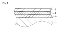
- FIG. 2 is a schematic cross-sectional view showing a part of the cross section of the terminal described in Embodiment 1.
- FIG. 3 is a graph showing test results of Test Example 1.
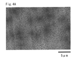
- FIG. 4A is a diagram showing a backscattered electron image of sample A.
- FIG. 4B is a diagram showing a binarized image of sample A.
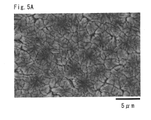
- FIG. 5A is a diagram showing a backscattered electron image of sample B.
- FIG. 5B is a diagram showing a binarized image of sample B.
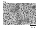
- FIG. 6A is a diagram showing a backscattered electron image of sample C.
- FIG. 6B is a diagram showing a binarized image of sample C.
- FIG. 6A is a diagram showing a backscattered electron image of sample C.
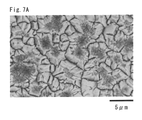
- FIG. 7A is a diagram showing a backscattered electron image of sample D.
- FIG. 7B is a diagram showing a binarized image of sample D.
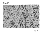
- FIG. 8A is a diagram showing a backscattered electron image of sample E.
- FIG. 8B is a diagram showing a binarized image of sample E.
- Patent Document 1 As shown in the manufacturing method referring to FIG. 2 of Patent Document 1, a nickel plating layer, a copper plating layer, and an indium plating layer are sequentially formed on the surface of a base material, and heat treatment is performed. ing.
- the terminal of the present disclosure has excellent productivity while having an indium layer on the outermost surface.
- the electric wire with terminal of the present disclosure has excellent productivity because it includes the terminal of the present disclosure, which is excellent in productivity.
- the method for manufacturing the terminal of the present disclosure can manufacture the terminal of the present disclosure with good productivity.
- the present inventors examined the number of coating layers formed on the base material and the constituent elements of the coating layers in fabricating a terminal having an indium layer on the outermost surface. First, a terminal in which a nickel layer is formed directly on a base material and an indium layer is formed at least partly directly on the nickel layer was examined. However, in this terminal, since the melting point of indium is low, interdiffusion easily occurs between the nickel layer and the indium layer in a high-temperature environment such as an in-vehicle environment.
- the inventors of the present invention conducted further studies and found that by artificially forming an intermetallic compound layer having a thickness of a certain value or more between the nickel layer and the indium layer, the mutual interaction between the indium layer and the nickel layer was improved. It was found that diffusion can be suppressed dramatically.
- the present disclosure has been made based on the above findings.
- the terminal according to the embodiment is A terminal-shaped base material made of copper or a copper alloy; a nickel layer disposed on at least part of the surface of the base material; an IMC (intermetallic compound) layer disposed on at least a portion directly above the nickel layer; an indium layer disposed immediately above the IMC layer;
- the IMC layer is composed of an intermetallic compound containing nickel and indium,
- the IMC layer has an average thickness of 0.13 ⁇ m or more.
- the IMC layer is formed between the nickel layer and the indium layer even at room temperature.
- the average thickness of the IMC layer formed at normal temperature is about 0.1 ⁇ m.
- the IMC layer is difficult to grow as long as it is in a normal temperature and normal pressure environment. In other words, it can be said that an IMC layer with an average thickness of 0.13 ⁇ m or more is an artificially grown IMC layer.
- the terminal according to the above embodiment is manufactured by simply forming a nickel layer and an indium layer on the surface of a base material in sequence and then performing heat treatment, as shown in the terminal manufacturing method described later. Therefore, the terminal according to the embodiment is excellent in productivity.
- the artificially formed IMC layer effectively suppresses interdiffusion between the nickel layer and the indium layer.
- indium in the indium layer is less likely to be alloyed with nickel, and an increase in contact resistance of the terminal due to alloying is suppressed. Therefore, in the terminal according to the embodiment, the effect obtained by providing the indium layer on the outermost surface is maintained for a long period of time.
- the IMC layer may have an average thickness of 0.18 ⁇ m or more.
- the average thickness of the IMC layer is 0.18 ⁇ m or more, interdiffusion between the indium layer and the nickel layer can be further suppressed.
- An average thickness of the IMC layer may be 0.24 ⁇ m or less.
- the IMC layer is formed by part of the indium layer formed directly on the nickel layer. Therefore, the thicker the IMC layer, the thinner the indium layer. If the average thickness of the IMC layer is 0.24 ⁇ m or less, a sufficient thickness of the indium layer is ensured. As a result, the effect obtained by the indium layer is sufficiently exhibited.
- the area ratio of the low luminance region in the binarized image obtained by processing the backscattered electron image obtained under the first imaging condition under the first image processing condition may be 50% or less.
- the first imaging condition is the imaging device is a scanning electron microscope, The accelerating voltage of the scanning electron microscope is 15 kV, an object to be imaged is the surface of the IMC layer exposed from the indium layer;
- the first image processing condition is The number of luminance gradations is 256,
- the brightness threshold is 140.
- the IMC layer is formed by interdiffusion between the nickel layer and the indium layer due to heat treatment.
- the thickness of the IMC layer formed by heat treatment varies.
- a backscattered electron image captured by a scanning electron microscope is a grayscale image expressed with 256 levels of brightness.
- the penetration depth of the electron beam varies depending on the magnitude of the acceleration voltage.
- information on the nickel layer immediately below the IMC layer is included in a portion where the IMC layer is thin, resulting in low brightness. Therefore, the smaller the area of low luminance in the backscattered electron image, the larger the area of the IMC layer having a thickness equal to or greater than a certain value.
- the area ratio of the low-luminance region in the binarized image obtained by image processing the backscattered electron image of the surface of the IMC layer is 50% or less, the region having a certain thickness or more is sufficiently secured in the IMC layer. be done. As a result, the effect obtained by the indium layer is sufficiently exhibited.
- the electric wire with a terminal according to the embodiment an electric wire; and a terminal attached to the end of the electric wire,
- the terminal is a terminal according to the embodiment.
- the electric wire with terminal according to the embodiment has excellent productivity. This is because the terminal of the embodiment provided to the electric wire with terminal is excellent in productivity.
- the electric wire with terminal according to the embodiment can be easily connected to the mating terminal. This is because the indium layer provided on the outermost surface of the terminal reduces the frictional resistance between the terminal-equipped wire and the mating terminal.
- a method for manufacturing a terminal includes: A step of preparing a base material composed of copper or a copper alloy; forming a nickel layer on at least part of the surface of the base material; forming an indium layer on at least part of the surface of the nickel layer; and heat-treating the base material having the nickel layer and the indium layer at an ambient temperature equal to or higher than the melting point of indium.
- the terminal manufacturing method according to the embodiment can manufacture the terminal according to the embodiment. Due to the above heat treatment step, interdiffusion between nickel and indium rapidly progresses near the boundary between the nickel layer and the indium layer. As a result, a thick IMC layer is formed between the nickel layer and the indium layer. This IMC layer is thicker than the IMC layer formed at room temperature.
- the film formation process is performed only twice. Therefore, according to the terminal manufacturing method, a terminal having a low coefficient of friction and a low contact resistance can be manufactured with high productivity.
- An electric wire 1 with a terminal shown in FIG. Terminal 2 is connected to conductor 30 exposed from insulating coating 31 at the end of electric wire 3 .
- the terminal 2 of this example is a female terminal and includes a wire barrel 20 and an insulation barrel 21 . By gripping the conductor 30 with the wire barrel 20, the conductor 30 and the terminal 2 are electrically connected.
- the insulation barrel 21 grips the outer circumference of the insulation coating 31 of the electric wire 3 .
- One of the features of the electric wire with terminal 1 of this example is that the structure of the terminal 2 is different from that of the conventional one. The configuration of the terminal 2 will be described in detail below.
- the shape of the terminal 2 is not particularly limited.
- the terminal 2 of this example is not particularly limited to a female terminal.
- the terminal 2 may be a male terminal or a flat terminal.
- FIG. 2 schematically shows a part of the cross section of the terminal 2.
- terminal 2 includes base material 4 , nickel layer 5 , IMC layer 6 and indium layer 7 .
- FIG. 2 is a schematic diagram, and the thickness ratio of each layer in FIG. 2 differs from the actual one.
- the base material 4 has a terminal shape.
- the base material 4 is made of copper or a copper alloy.
- the copper alloy may be the same as the material of general copper terminals.
- the copper alloy is brass, phosphor bronze, or the like.
- the nickel layer 5 is formed on at least part of the base material 4 right above it.
- the nickel layer 5 is a layer in which 98% by mass or more of the constituent elements are nickel.
- the nickel layer 5 functions as a barrier layer that prevents copper contained in the base material 4 from diffusing into the indium layer 7 on the outermost surface.
- a boundary layer containing copper and nickel of the base material 4 is formed at the boundary with the base material 4 .
- the average thickness of the nickel layer 5 is preferably 0.1 ⁇ m or more and 10 ⁇ m or less. If the nickel layer 5 has an average thickness of 0.1 ⁇ m or more, diffusion of copper contained in the base material 4 into the indium layer 7 is sufficiently suppressed. If the nickel layer 5 has an average thickness of 10 ⁇ m or less, the time required to form the nickel layer 5 can be shortened.
- the lower limit of the nickel layer 5 may be 0.5 ⁇ m, or even 1 ⁇ m.
- the upper limit of the nickel layer 5 may be 5 ⁇ m, or even 3 ⁇ m. Therefore, the average thickness of the nickel layer 5 may be 0.5 ⁇ m or more and 5 ⁇ m or less, further 1 ⁇ m or more and 3 ⁇ m or less.
- the average thickness of the nickel layer 5 is obtained, for example, as follows.
- the thickness of the nickel layer 5 at a plurality of different locations in the portion of the terminal 2 that contacts the mating terminal is measured by a fluorescent X-ray film thickness meter.
- the number of terminals 2 to be measured is preferably three or more.
- the average thickness of the nickel layer 5 is obtained by dividing the total thickness measurements of the nickel layer 5 by the number of measurements.
- the IMC layer 6 is formed directly on the nickel layer 5 .
- the IMC layer 6 is a layer made of an intermetallic compound of nickel and indium.
- the IMC layer 6 is a layer in which 96% by mass or more of constituent elements are nickel and indium.
- the atomic ratio of nickel and indium in the IMC layer 6 is 3:7 or more and 4:6 or less. Since the nickel layer 5 serves as a barrier layer, the IMC layer 6 does not substantially contain copper.
- the IMC layer 6 functions as a barrier layer that suppresses mutual diffusion between the nickel layer 5 and the indium layer 7. IMC layer 6 prevents nickel contained in nickel layer 5 from diffusing into indium layer 7 . As a result, formation of an intermetallic compound of nickel and indium in the indium layer 7 is suppressed.
- the average thickness of the IMC layer 6 is 0.13 ⁇ m or more.
- the average thickness of the IMC layer 6 is obtained by the same measuring method as the average thickness of the nickel layer 5 . If the average thickness of IMC layer 6 is 0.13 ⁇ m or more, interdiffusion between nickel layer 5 and indium layer 7 is effectively suppressed. Therefore, even if the terminal 2 is repeatedly exposed to a high-temperature environment, an intermetallic compound is less likely to be formed in the indium layer 7 . for that reason. An increase in the contact resistance of the terminal 2 is suppressed over a long period of time.
- a high-temperature environment is, for example, the engine room of an automobile. In the engine room, the ambient temperature near the terminal 2 may approach the melting point of indium.
- the average thickness of the IMC layer 6 is preferably 0.18 ⁇ m or more.
- the average thickness of the IMC layer 6 is preferably 0.24 ⁇ m or less.
- the average thickness of the IMC layer 6 is obtained, for example, as follows. First, the indium layer 7 is removed from the surface of the terminal 2 by selective etching or the like. Next, the thickness of the IMC layer 6 at a plurality of different locations in the portion of the terminal 2 that contacts the mating terminal is measured by a fluorescent X-ray film thickness meter. The number of terminals 2 to be measured is preferably three or more. The average thickness of the IMC layer 6 is determined by dividing the sum of the thickness measurements of the IMC layer 6 by the number of measurements.
- the thickness of the IMC layer 6 varies.
- it is preferable that the proportion of portions where the thickness of the IMC layer 6 is thin is as small as possible.
- the ratio of the portions where the thickness of the IMC layer 6 is thin is the area ratio of the low-luminance region in the binarized image obtained by processing the backscattered electron image obtained under the first imaging condition under the first image processing condition as follows. Obtained by measuring.
- a backscattered electron image is obtained as follows. First, the indium layer 7 is removed from the surface of the terminal 2 by selective etching or the like. A backscattered electron image of the surface of the IMC layer 6 is taken by SEM. The acceleration voltage of SEM is 15 kV. The magnification is 5000 times. The area of the backscattered electron image is, for example, 300 ⁇ m 2 or more and 1200 ⁇ m 2 or less.
- the captured backscattered electron image is image-processed as follows.
- a brightness value histogram of 256 gradations from 0 to 255 is obtained from the backscattered electron image.
- the horizontal axis of the luminance value histogram represents the luminance value, and the vertical axis represents the number of pixels. The closer the luminance value is to 0, the darker it is, and the closer the luminance value is to 255, the brighter it is.
- the brightness of the backscattered electron image is adjusted to obtain an image converted to brightness of 256 gradations with the minimum value of the brightness value histogram being 0 and the maximum value of the brightness value histogram being 255.
- a binarized image is generated by binarizing the image whose luminance has been converted, and a low luminance area is extracted.
- a binarized image is an image that has been subjected to binarization processing with a brightness threshold of 140 set.
- a region with a luminance of 140 or less is a low-luminance region, and a region with a luminance of more than 140 is a high-luminance region.
- a low luminance area is an area where the thickness of the IMC layer 6 is thin.
- a high luminance region is a region where the IMC layer 6 has a thickness equal to or greater than a certain value. The reason why the brightness differs depending on the thickness of the IMC layer 6 is that the nickel layer 5 affects the brightness at a portion where the IMC layer 6 is thin in the backscattered electron image.
- the area ratio of the low-luminance region is the ratio of the area of the low-luminance region to the area of the binarized image expressed in percentage.
- the area ratio of the low-brightness region is an index of the ratio of portions where the thickness of the IMC layer 6 is thin. The smaller the area ratio of the low luminance region, the smaller the ratio of the region where the thickness of the IMC layer 6 is thin.
- the area ratio of the low-luminance region is 50% or less, a region having a certain thickness or more is sufficiently secured in the IMC layer 6 . As a result, interdiffusion between the nickel layer 5 and the indium layer 7 is effectively suppressed.
- the area ratio of the low luminance region may be 45% or less, 40% or less, or 30% or less.
- the lower limit of the area ratio of the low luminance region may be zero.
- the area ratio of the low luminance region may be, for example, 0 to 50%, 5% to 45%, or 10% to 40%.
- Indium layer 7 is formed directly on IMC layer 6 .
- the indium layer 7 is a layer in which 96% by mass or more of the constituent elements is indium.
- the indium layer 7 reduces the friction coefficient of the surface of the terminal 2 and reduces the terminal insertion force. Indium layer 7 also reduces contact resistance on the surface of terminal 2 .
- the average thickness of the indium layer 7 is preferably 0.05 ⁇ m or more and 10 ⁇ m or less, for example. If the average thickness of the indium layer 7 is 0.05 ⁇ m or more, the frictional resistance on the surface of the terminal 2 is sufficiently reduced. If the average thickness of the indium layer 7 is 10 ⁇ m or less, the amount of expensive indium used can be reduced.
- the average thickness of the indium layer 7 is preferably 1 ⁇ m or more.
- the artificially formed IMC layer 6 effectively suppresses interdiffusion between the nickel layer 5 and the indium layer 7 .
- indium in the indium layer 7 is less likely to be alloyed with nickel, and an increase in contact resistance of the terminal 2 due to alloying is suppressed. Therefore, in the terminal 2 of this example, the effect obtained by providing the indium layer 7 on the outermost surface is maintained for a long period of time.
- the terminal 2 according to the embodiment is manufactured, for example, by the following steps. - Step A of preparing a base material 4 made of copper or a copper alloy - Step B of forming a nickel layer 5 on at least part of the surface of the base material - Step C of plating an indium layer 7 on at least part of the surface of the nickel layer 5 - Step D of heat-treating the base material 4 having the nickel layer 5 and the indium layer 7 at an ambient temperature equal to or higher than the melting point of indium.
- a base material 4 is prepared.
- the base material 4 may have a terminal shape, or may have a raw material shape before being formed into a terminal shape.
- terminal 2 in this example is a female terminal. Therefore, the base material 4 may be a plate material, or may be formed by pressing a plate material into a terminal shape.
- a nickel layer 5 is formed on at least part of the surface of the base material 4 .
- the nickel layer 5 is formed by plating, sputtering, vapor deposition, or the like.
- the plating method may be an electrolytic plating method, an electroless plating method, or a hot dip plating method. Plating, sputtering, and vapor deposition are performed according to known conditions.
- the base material 4 is pretreated.
- the pretreatments are degreasing, pickling and water washing. Degreasing, pickling, and water washing are carried out by known methods.
- step C an indium layer 7 is formed on at least part of the surface of the nickel layer 5 .
- the indium layer 7 is formed by plating, sputtering, vapor deposition, or the like. Plating, sputtering, and vapor deposition are performed according to known conditions.
- the base material 4 with the nickel layer 5 is washed with water.
- step D the base material 4 having the nickel layer 5 and the indium layer 7 is heat-treated.
- the heat treatment is performed at an ambient temperature of 156.6° C. or higher, which is the melting point of indium. This heat treatment forms an IMC layer 6 between the nickel layer 5 and the indium layer 7 .
- the ambient temperature is 156.6°C or higher, which is the melting point of indium.
- the ambient temperature is preferably 156.6°C or higher and 300°C or lower.
- a more preferable ambient temperature is 200° C. or higher, and a further preferable ambient temperature is 220° C. or higher.
- the atmosphere may be an air atmosphere or a nitrogen atmosphere.
- the heat treatment time is preferably 5 seconds or more and 60 seconds or less. If the heat treatment time is 5 seconds or more, the average thickness of the IMC layer 6 tends to be 0.13 ⁇ m or more. The longer the processing time, the thicker the average thickness of the IMC layer 6 . If the ambient temperature is higher, the treatment time may be shorter.
- the above heat treatment is performed, for example, by a reflow furnace.
- the IMC layer 6 is formed while the base material 4 is passing through a reflow furnace at a predetermined ambient temperature.
- the heat treatment time depends on the length of the reflow furnace. Therefore, in order to adjust the average thickness of the IMC layer 6 using one reflow furnace, the ambient temperature in the reflow furnace is changed.
- the terminal manufacturing method of this example can manufacture the terminal 2 of this example with high productivity. As described above, only two layers, the nickel layer 5 and the indium layer 7, are required for the film forming process when fabricating the terminal 2 of this example. Also, the IMC layer 6 is formed by heat treatment for a very short time. Therefore, according to the terminal manufacturing method of this example, the terminal 2 can be manufactured with high productivity.
- heat treatment using a reflow furnace a large number of terminals 2 can be heat treated continuously. Moreover, heat treatment using a reflow furnace allows strict control of the heat treatment time. In the batch furnace, excessive heat may be applied to the terminal 2 until the terminal 2 is removed from the batch furnace after the heat treatment.
- Test Example 1 In Test Example 1, the influence of the average thickness of the IMC layer 6 on the heat resistance of the terminal 2 was investigated. First, terminals of samples A, B, C, D, and E having different average thicknesses of the IMC layers 6 were produced. The manufacturing procedure of each terminal is as follows.
- a plurality of plate-like base materials made of phosphor bronze were prepared.
- a nickel layer and an indium layer were sequentially formed on the surface of each base material.
- the nickel layer and the indium layer were formed by electroplating.
- a base sample is obtained by forming a nickel layer and an indium layer on a base material. Some base samples were not heat treated. Sample A is the base sample that was not heat treated. The remaining base samples were divided into four groups and different heat treatments were applied to each group. In the heat treatment, after introducing the base sample into a reflow furnace preheated to a predetermined temperature, the temperature of the reflow furnace was raised to the main heating temperature.
- the preheating temperature of the reflow furnace, the main heating temperature of the reflow furnace, and the time for the base sample to pass through the reflow furnace for obtaining Sample B, Sample C, Sample D, and Sample E are as follows. ⁇ Sample B: preheating temperature: 160°C, main heating temperature: 200°C, time: 13 seconds ⁇ Sample C: preheating temperature: 140°C, main heating temperature: 220°C, time: 13 seconds ⁇ Sample D: preheating temperature: 160 ° C., main heating temperature: 220 ° C., time: 26 seconds Sample E ... preheating temperature: 180 ° C., main heating temperature: 220 ° C., time: 13 seconds
- the average thickness of the IMC layer of each sample was obtained as follows. First, three terminals for each of samples A, B, C, D, and E were prepared. The indium layer of each terminal was removed by selective etching to expose the IMC layer. The thickness of the exposed IMC layer at two different locations was measured by a calibration curve method using a fluorescent X-ray film thickness gauge. The portion where the IMC layer is measured corresponds to the portion where the terminal of the sample contacts the mating terminal.
- the fluorescent X-ray film thickness gauge was FT-150 manufactured by Hitachi High-Tech Science Co., Ltd. The sum of the six measurements obtained from each sample divided by six is the average thickness of the IMC layer for each sample. Table 1 shows the average thickness of each sample.
- the area ratio of the low-brightness region was obtained from the backscattered electron image of the surface of the IMC layer of each sample.
- the area ratio of the low luminance region was obtained as follows. First, terminals of samples A, B, C, D, and E were prepared. The indium layer of each terminal was removed by selective etching to expose the IMC layer. The exposed surface of the IMC layer was imaged using an SEM to obtain a backscattered electron image. The acceleration voltage of SEM was set to 15 kV. The magnification was 5000 times. The area of the captured backscattered electron image was about 500 ⁇ m 2 . JSM-6480 manufactured by JEOL Ltd. was used as the SEM. The captured backscattered electron image was imported into image processing software.
- a brightness value histogram of 256 gradations from 0 to 255 was obtained from the backscattered electron image. Then, the backscattered electron image was subjected to image processing and converted into luminance of 256 gradations, where 0 is the minimum value of the luminance value histogram and 255 is the maximum value of the luminance value histogram. The converted image was binarized to generate a binarized image. A luminance threshold value of 140 was set for the binarization process. A low-luminance region was extracted from the generated binarized image, and the area ratio of the low-luminance region was calculated. "Image J" was used as the image processing software. Table 1 shows the area ratio of the low-luminance region of each sample.
- the backscattered electron image of sample A shown in FIG. 4A has many dark regions and few bright regions as a whole.
- FIG. 4B in the binarized image of the sample A, the percentage of low-brightness regions that appear black is large.
- the backscattered electron images of samples B, C, D, and E shown in FIGS. 5A to 8A have fewer dark regions and more bright regions than the backscattered electron image of sample A shown in FIG. 4A. . Therefore, as shown in FIGS. 5B to 8B, in each of the binarized images of samples B, C, D, and E, the percentage of low-brightness regions that appear black is small.
- the reason why the IMC layer was formed in the sample A which was not subjected to the heat treatment is presumed to be that indium is easily alloyed with nickel when the indium layer is formed by electroplating.
- the horizontal axis of the graph in FIG. 3 is the average thickness ( ⁇ m) of the IMC layer before the heat resistance test, and the vertical axis is the alloying rate ( ⁇ m/hr).
- the alloying rates of samples A, B, C, D and E are plotted in the graph.
- the straight line in the figure is a straight line showing the correlation between the average thickness of the IMC layer before the test and the alloying speed.
- the straight lines in the graph are approximate lines obtained from the alloying rates of samples B, C, D, and E by the method of least squares. As is clear from this graph, the alloying speeds of samples B, C, D and E were significantly lower than that of sample A in an atmosphere of 125°C.
- the alloying of the indium layer can be greatly delayed if the average thickness of the IMC layer is 0.13 ⁇ m or more. Therefore, it is believed that the terminal 2 of the embodiment having the IMC layer 6 with an average thickness of 0.13 ⁇ m or more can maintain its performance over a long period of time in an in-vehicle environment.
- the alloying speed becomes slower as the average thickness of the IMC layer before the test increases. From this result, it has become clear that increasing the average thickness of the IMC layer is effective in improving the heat resistance of the terminal 2 .
Landscapes
- Chemical & Material Sciences (AREA)
- Engineering & Computer Science (AREA)
- Manufacturing & Machinery (AREA)
- Chemical Kinetics & Catalysis (AREA)
- Materials Engineering (AREA)
- Mechanical Engineering (AREA)
- Metallurgy (AREA)
- Organic Chemistry (AREA)
- Electroplating Methods And Accessories (AREA)
Abstract
銅又は銅合金によって構成される端子形状の母材と、前記母材の表面の少なくとも一部に配置されるニッケル層と、前記ニッケル層の直上の少なくとも一部に配置されるIMC層と、前記IMC層の直上に配置されるインジウム層とを備え、前記IMC層は、ニッケルとインジウムを含む金属間化合物によって構成され、前記IMC層の平均厚さが0.13μm以上である、端子。
Description
本開示は、端子、端子付き電線、及び端子の製造方法に関する。
本出願は、2021年3月19日付の日本国出願の特願2021-046404に基づく優先権を主張し、前記日本国出願に記載された全ての記載内容を援用するものである。
本出願は、2021年3月19日付の日本国出願の特願2021-046404に基づく優先権を主張し、前記日本国出願に記載された全ての記載内容を援用するものである。
特許文献1には、銅又は銅合金の母材と、母材の表面に形成される複数の被覆層とを備える接続用端子が開示されている。複数の被覆層は、母材の表面から順に、下地めっき層、硬質めっき層、及び表面めっき層を含む。下地めっき層はニッケル又はニッケル合金によって構成されている。硬質めっき層は銅とインジウムを含む金属間化合物によって構成されている。表面めっき層はインジウム又はインジウム合金によって構成されている。表面めっき層は、端子の最表面に配置される層である。
インジウムを含む表面めっき層の効果には、インジウムめっき端子と相手端子との間の摩擦係数を低減できるという効果、及びインジウムめっき端子と相手端子との間の接触抵抗を低減できるという効果がある。反面、インジウムの融点が低いため、インジウムを含む表面めっき層は耐熱性に劣るという問題がある。この表面めっき層が、インジウムの融点に迫る高温環境にさらされた場合、母材に含まれる銅などが表面めっき層に拡散し、金属間化合物が形成される。金属間化合物が端子の最表面に露出すると、端子の接触抵抗が増加してしまう。特許文献1では、下地めっき層によって、母材に含まれる銅が表面めっき層に拡散することが抑制されている。また、硬質めっき層によって、下地めっき層に含まれるニッケルなどが表面めっき層に拡散することが抑制されている。
本開示の端子は、
銅又は銅合金によって構成される端子形状の母材と、
前記母材の表面の少なくとも一部に配置されるニッケル層と、
前記ニッケル層の直上の少なくとも一部に配置されるIMC層と、
前記IMC層の直上に配置されるインジウム層とを備え、
前記IMC層は、ニッケルとインジウムを含む金属間化合物によって構成され、
前記IMC層の平均厚さが0.13μm以上である。
銅又は銅合金によって構成される端子形状の母材と、
前記母材の表面の少なくとも一部に配置されるニッケル層と、
前記ニッケル層の直上の少なくとも一部に配置されるIMC層と、
前記IMC層の直上に配置されるインジウム層とを備え、
前記IMC層は、ニッケルとインジウムを含む金属間化合物によって構成され、
前記IMC層の平均厚さが0.13μm以上である。
本開示の端子付き電線は、
電線と、
前記電線の端部に取付けられた端子とを備え、
前記端子は、本開示の端子である。
電線と、
前記電線の端部に取付けられた端子とを備え、
前記端子は、本開示の端子である。
本開示の端子の製造方法は、
銅又は銅合金によって構成される母材を用意する工程と、
前記母材の表面の少なくとも一部にニッケル層を形成する工程と、
前記ニッケル層の表面の少なくとも一部にインジウム層を形成する工程と、
前記ニッケル層と前記インジウム層とを有する前記母材をインジウムの融点以上の雰囲気温度で熱処理する工程とを含む。
銅又は銅合金によって構成される母材を用意する工程と、
前記母材の表面の少なくとも一部にニッケル層を形成する工程と、
前記ニッケル層の表面の少なくとも一部にインジウム層を形成する工程と、
前記ニッケル層と前記インジウム層とを有する前記母材をインジウムの融点以上の雰囲気温度で熱処理する工程とを含む。
[本開示が解決しようとする課題]
端子の生産性の観点から、端子の製造時に母材上に設けられる被覆層の数を減らしたいというニーズがある。特許文献1では、特許文献1の図2を参照する製造方法に示されるように、母材の表面に順次、ニッケルめっき層と、銅めっき層と、インジウムめっき層を形成し、更に熱処理を行っている。
端子の生産性の観点から、端子の製造時に母材上に設けられる被覆層の数を減らしたいというニーズがある。特許文献1では、特許文献1の図2を参照する製造方法に示されるように、母材の表面に順次、ニッケルめっき層と、銅めっき層と、インジウムめっき層を形成し、更に熱処理を行っている。
上記事情に鑑み、本開示は、最表面にインジウム層を備えながらも生産性に優れる端子と、その端子の製造方法を提供することを目的の一つとする。また、本開示は、最表面にインジウム層を有する端子を備える端子付き電線を提供することを目的の一つとする。
[本開示の効果]
本開示の端子は、最表面にインジウム層を備えながらも生産性に優れる。
本開示の端子は、最表面にインジウム層を備えながらも生産性に優れる。
本開示の端子付き電線は、生産性に優れる本開示の端子を備えるため、生産性に優れる。
本開示の端子の製造方法は、本開示の端子を生産性良く製造できる。
[本開示の実施形態の説明]
本発明者らは、最表面にインジウム層を備える端子を作製するにあたり、母材上に形成する被覆層の数、及び被覆層の構成元素を検討した。まず、母材の直上にニッケル層を形成し、ニッケル層の直上の少なくとも一部にインジウム層を形成した端子を検討した。しかし、この端子では、インジウムの融点が低いことから、車載環境などの高温環境においてニッケル層とインジウム層との間で相互拡散が生じ易い。そこで、本発明者らは更に検討を重ね、ニッケル層とインジウム層との間に人為的に一定以上の厚さの金属間化合物層を形成することで、インジウム層とニッケル層との間の相互拡散を劇的に抑制できることを見出した。本開示は上記知見に基づいて得られたものである。
本発明者らは、最表面にインジウム層を備える端子を作製するにあたり、母材上に形成する被覆層の数、及び被覆層の構成元素を検討した。まず、母材の直上にニッケル層を形成し、ニッケル層の直上の少なくとも一部にインジウム層を形成した端子を検討した。しかし、この端子では、インジウムの融点が低いことから、車載環境などの高温環境においてニッケル層とインジウム層との間で相互拡散が生じ易い。そこで、本発明者らは更に検討を重ね、ニッケル層とインジウム層との間に人為的に一定以上の厚さの金属間化合物層を形成することで、インジウム層とニッケル層との間の相互拡散を劇的に抑制できることを見出した。本開示は上記知見に基づいて得られたものである。
最初に本開示の実施形態の内容を列記して説明する。
<1>実施形態に係る端子は、
銅又は銅合金によって構成される端子形状の母材と、
前記母材の表面の少なくとも一部に配置されるニッケル層と、
前記ニッケル層の直上の少なくとも一部に配置されるIMC(Intermetallic compounds)層と、
前記IMC層の直上に配置されるインジウム層とを備え、
前記IMC層は、ニッケルとインジウムを含む金属間化合物によって構成され、
前記IMC層の平均厚さが0.13μm以上である。
銅又は銅合金によって構成される端子形状の母材と、
前記母材の表面の少なくとも一部に配置されるニッケル層と、
前記ニッケル層の直上の少なくとも一部に配置されるIMC(Intermetallic compounds)層と、
前記IMC層の直上に配置されるインジウム層とを備え、
前記IMC層は、ニッケルとインジウムを含む金属間化合物によって構成され、
前記IMC層の平均厚さが0.13μm以上である。
後述する試験例に示されるように、ニッケル層の直上の少なくとも一部にインジウム層を形成すれば、ニッケル層とインジウム層との間にIMC層が常温においても形成される。常温において形成されたIMC層の平均厚さは0.1μm程度である。そのIMC層は、常温・常圧環境下にある限り成長し難い。つまり、平均厚さが0.13μm以上のIMC層は、人為的に成長させられたIMC層であると言える。
上記実施形態に係る端子は、後述する端子の製造方法に示されるように、母材の表面に順次、ニッケル層とインジウム層を形成した後、熱処理を行うだけで作製される。従って、実施形態に係る端子は生産性に優れる。
実施形態の端子では、人為的に形成されたIMC層が、ニッケル層とインジウム層との間の相互拡散を効果的に抑制する。その結果、実施形態に係る端子が高温環境にさらされても、インジウム層のインジウムがニッケルと合金化し難く、合金化に伴う端子の接触抵抗の増加が抑制される。従って、実施形態に係る端子では、最表面にインジウム層が設けられたことによって得られる効果が長期にわたって維持される。
<2>実施形態に係る端子において、
前記IMC層の平均厚さが0.18μm以上であってもよい。
前記IMC層の平均厚さが0.18μm以上であってもよい。
IMC層の平均厚さが0.18μm以上であれば、より一層、インジウム層とニッケル層との間の相互拡散を抑制できる。
<3>実施形態に係る端子において、
前記IMC層の平均厚さが0.24μm以下であってもよい。
前記IMC層の平均厚さが0.24μm以下であってもよい。
後述する端子の製造方法に記載されるように、IMC層は、ニッケル層の直上に形成されたインジウム層の一部によって形成される。従って、IMC層が厚くなるほど、インジウム層が薄くなる。IMC層の平均厚さが0.24μm以下であれば、インジウム層の厚さが十分に確保される。その結果、インジウム層によって得られる効果が十分に発揮される。
<4>実施形態に係る端子において、
第一撮像条件で得られた反射電子像を第一画像処理条件で処理した2値化画像における低輝度領域の面積率が50%以下であってもよい。
前記第一撮像条件は、
撮像装置が走査型電子顕微鏡であり、
前記走査型電子顕微鏡の加速電圧が15kVであり、
撮像対象が、前記インジウム層から露出された前記IMC層の表面であり、
前記第一画像処理条件は、
輝度の階調数が256であり、
輝度の閾値が140である。
第一撮像条件で得られた反射電子像を第一画像処理条件で処理した2値化画像における低輝度領域の面積率が50%以下であってもよい。
前記第一撮像条件は、
撮像装置が走査型電子顕微鏡であり、
前記走査型電子顕微鏡の加速電圧が15kVであり、
撮像対象が、前記インジウム層から露出された前記IMC層の表面であり、
前記第一画像処理条件は、
輝度の階調数が256であり、
輝度の閾値が140である。
後述する端子の製造方法に記載されるように、IMC層は、熱処理によってニッケル層とインジウム層との間で相互拡散が生じることによって形成される。熱処理によって形成されたIMC層の厚さはばらつきがある。
走査型電子顕微鏡(SEM)によって撮像された反射電子像は256階調の輝度で表現されたグレースケール画像である。SEMは加速電圧の大きさによって、電子ビームが侵入する深さが異なる。加速電圧が15kVで撮像された反射電子像において、IMC層が薄い箇所では、IMC層の直下にあるニッケル層の情報が含まれ、輝度が低くなる。従って、反射電子像において低輝度の領域が小さいほど、IMC層において一定以上の厚さを有する領域が大きい。IMC層の表面の反射電子像を画像処理して得られた2値化画像における低輝度領域の面積率が50%以下であれば、IMC層において一定以上の厚さを有する領域が十分に確保される。その結果、インジウム層によって得られる効果が十分に発揮される。
<5>実施形態に係る端子付き電線は、
電線と、
前記電線の端部に取付けられた端子とを備え、
前記端子は、実施形態に係る端子である。
電線と、
前記電線の端部に取付けられた端子とを備え、
前記端子は、実施形態に係る端子である。
実施形態に係る端子付き電線は、生産性に優れる。端子付き電線に備わる実施形態の端子が生産性に優れるからである。
実施形態に係る端子付き電線は、相手端子と接続し易い。端子の最表面に設けられるインジウム層が、端子付き電線と相手端子との間の摩擦抵抗を低減させるからである。
<6>実施形態に係る端子の製造方法は、
銅又は銅合金によって構成される母材を用意する工程と、
前記母材の表面の少なくとも一部にニッケル層を形成する工程と、
前記ニッケル層の表面の少なくとも一部にインジウム層を形成する工程と、
前記ニッケル層と前記インジウム層とを有する前記母材をインジウムの融点以上の雰囲気温度で熱処理する工程とを含む。
銅又は銅合金によって構成される母材を用意する工程と、
前記母材の表面の少なくとも一部にニッケル層を形成する工程と、
前記ニッケル層の表面の少なくとも一部にインジウム層を形成する工程と、
前記ニッケル層と前記インジウム層とを有する前記母材をインジウムの融点以上の雰囲気温度で熱処理する工程とを含む。
実施形態に係る端子の製造方法は、実施形態に係る端子を製造できる。
上記熱処理する工程によって、ニッケル層とインジウム層との境界付近でニッケルとインジウムとの相互拡散が急激に進行する。その結果、ニッケル層とインジウム層との間に、IMC層が厚く形成される。このIMC層は、常温において形成されるIMC層よりも厚い。
上記熱処理する工程によって、ニッケル層とインジウム層との境界付近でニッケルとインジウムとの相互拡散が急激に進行する。その結果、ニッケル層とインジウム層との間に、IMC層が厚く形成される。このIMC層は、常温において形成されるIMC層よりも厚い。
上記端子の製造方法では、成膜工程は2回のみである。従って、上記端子の製造方法によれば、摩擦係数と接触抵抗が低い端子を生産性良く製造できる。
[本開示の実施形態の詳細]
以下、図面を適宜参照して、本開示の実施の形態を詳細に説明する。図中の同一符号は、同一名称物を示す。本発明は、実施形態の例示に限定されるものではなく、請求の範囲によって示され、請求の範囲と均等の意味及び範囲内での全ての変更が含まれることが意図される。
以下、図面を適宜参照して、本開示の実施の形態を詳細に説明する。図中の同一符号は、同一名称物を示す。本発明は、実施形態の例示に限定されるものではなく、請求の範囲によって示され、請求の範囲と均等の意味及び範囲内での全ての変更が含まれることが意図される。
<実施形態1>
図1に示される端子付き電線1は、端子2と電線3とを備える、電線3は、導体30と導体30の外周を被覆する絶縁被覆31とを備える。端子2は、電線3の端部において絶縁被覆31から露出される導体30に接続されている。本例の端子2はメス端子であって、ワイヤバレル20とインシュレーションバレル21とを備えている。ワイヤバレル20が導体30を把持することで、導体30と端子2とが電気的に接続される。インシュレーションバレル21は、電線3の絶縁被覆31の外周を把持している。本例の端子付き電線1の特徴の一つは、端子2の構成が従来と異なる点にある。以下、端子2の構成を詳細に説明する。
図1に示される端子付き電線1は、端子2と電線3とを備える、電線3は、導体30と導体30の外周を被覆する絶縁被覆31とを備える。端子2は、電線3の端部において絶縁被覆31から露出される導体30に接続されている。本例の端子2はメス端子であって、ワイヤバレル20とインシュレーションバレル21とを備えている。ワイヤバレル20が導体30を把持することで、導体30と端子2とが電気的に接続される。インシュレーションバレル21は、電線3の絶縁被覆31の外周を把持している。本例の端子付き電線1の特徴の一つは、端子2の構成が従来と異なる点にある。以下、端子2の構成を詳細に説明する。
≪端子≫
端子2の形状は特に限定されない。本例の端子2は、特にメス端子に限定されるわけではない。例えば端子2は、オス端子でも良いし、平端子でも良い。
端子2の形状は特に限定されない。本例の端子2は、特にメス端子に限定されるわけではない。例えば端子2は、オス端子でも良いし、平端子でも良い。
端子2の被覆層の構成については図2を参照して説明する。図2は、端子2の断面の一部を模式的に示している。図2に示されるように、端子2は、母材4と、ニッケル層5と、IMC層6と、インジウム層7とを備える。ここで、図2は模式図であり、図2における各層の厚さの比率は、実際とは異なる。
(母材)
母材4は、端子形状を備える。母材4は銅又は銅合金によって構成される。銅合金は、一般的な銅端子の材料と同じもので良い。例えば、銅合金は、黄銅又はリン青銅などである。
母材4は、端子形状を備える。母材4は銅又は銅合金によって構成される。銅合金は、一般的な銅端子の材料と同じもので良い。例えば、銅合金は、黄銅又はリン青銅などである。
(ニッケル層)
ニッケル層5は、母材4の直上の少なくとも一部に形成されている。ニッケル層5は、構成元素の98質量%以上がニッケルからなる層である。ニッケル層5は、母材4に含まれる銅が最表面のインジウム層7に拡散することを抑制するバリア層として機能する。母材4との境界には、母材4の銅とニッケルとを含む境界層が形成されている。
ニッケル層5は、母材4の直上の少なくとも一部に形成されている。ニッケル層5は、構成元素の98質量%以上がニッケルからなる層である。ニッケル層5は、母材4に含まれる銅が最表面のインジウム層7に拡散することを抑制するバリア層として機能する。母材4との境界には、母材4の銅とニッケルとを含む境界層が形成されている。
ニッケル層5の平均厚さは、0.1μm以上10μm以下であることが好ましい。ニッケル層5の平均厚さが0.1μm以上であれば、母材4に含まれる銅のインジウム層7への拡散が十分に抑制される。ニッケル層5の平均厚さが10μm以下であれば、ニッケル層5を形成する時間が短くて済む。ニッケル層5の下限は、0.5μm、更には1μmであっても良い。ニッケル層5の上限は、5μm、更には3μmであっても良い。従って、ニッケル層5の平均厚さは、0.5μm以上5μm以下、更には1μm以上3μm以下であっても良い。
ニッケル層5の平均厚さは、例えば以下のようにして求められる。端子2のうち、相手端子と接触する部分における異なる複数箇所のニッケル層5の厚さを蛍光X線膜厚計によって測定する。測定する端子2の数は3つ以上とすることが好ましい。ニッケル層5の厚さの測定値の合計を測定数で割れば、ニッケル層5の平均厚さが求められる。
(IMC層)
IMC層6は、ニッケル層5の直上に形成されている。IMC層6は、ニッケルとインジウムとの金属間化合物によって構成される層である。IMC層6は、構成元素の96質量%以上がニッケル及びインジウムからなる層である。IMC層6におけるニッケルとインジウムの原子比は、3:7以上4:6以下である。ニッケル層5がバリア層となっているため、IMC層6には実質的に銅は含まれない。
IMC層6は、ニッケル層5の直上に形成されている。IMC層6は、ニッケルとインジウムとの金属間化合物によって構成される層である。IMC層6は、構成元素の96質量%以上がニッケル及びインジウムからなる層である。IMC層6におけるニッケルとインジウムの原子比は、3:7以上4:6以下である。ニッケル層5がバリア層となっているため、IMC層6には実質的に銅は含まれない。
IMC層6は、ニッケル層5とインジウム層7との間の相互拡散を抑制するバリア層として機能する。IMC層6によって、ニッケル層5に含まれるニッケルがインジウム層7に拡散することが抑制される。その結果、インジウム層7におけるニッケルとインジウムとの金属間化合物の形成が抑制される。
IMC層6の平均厚さは0.13μm以上である。IMC層6の平均厚さは、ニッケル層5の平均厚さの測定方法と同様の測定方法によって求められる。IMC層6の平均厚さが0.13μm以上であれば、ニッケル層5とインジウム層7との間の相互拡散が効果的に抑制される。従って、端子2が繰り返し高温環境にさらされても、インジウム層7に金属間化合物が形成され難い。そのため。長期にわたって端子2の接触抵抗の上昇が抑制される。高温環境は、例えば自動車のエンジンルーム内である。エンジンルーム内では、端子2の近傍の雰囲気温度が、インジウムの融点に迫る温度となる場合がある。
相互拡散の抑制効果は、IMC層6の平均厚さに依存する。従って、IMC層6の平均厚さは0.18μm以上であることが好ましい。一方、IMC層6の平均厚さは0.24μm以下であることが好ましい。
IMC層6の平均厚さは、例えば以下のようにして求められる。まず、選択的エッチングなどで、端子2の表面からインジウム層7を除去する。次いで、端子2のうち、相手端子と接触する部分における異なる複数箇所のIMC層6の厚さを蛍光X線膜厚計によって測定する。測定する端子2の数は3つ以上とすることが好ましい。IMC層6の厚さの測定値の合計を測定数で割ることでIMC層6の平均厚さが求められる。
IMC層6の厚さはばらつきがある。IMC層6において一定以上の厚さを有する領域が大きいほど、相互拡散の抑制効果が高い。換言すれば、IMC層6の厚さが薄い箇所の割合が小さいほど好ましい。IMC層6の厚さが薄い箇所の割合は、以下のように、第一撮像条件で得られた反射電子像を第一画像処理条件で処理した2値化画像における低輝度領域の面積率を測定することで求められる。
反射電子像は次のようにして得られる。まず、選択的エッチングなどで、端子2の表面からインジウム層7を除去する。IMC層6の表面の反射電子像をSEMによって撮像する。SEMの加速電圧は15kVである。倍率は5000倍である。反射電子像の面積は、例えば300μm2以上1200μm2以下である。
撮像された反射電子像は次のようにして画像処理される。反射電子像から輝度値が0から255までの256階調の輝度値ヒストグラムを取得する。輝度値ヒストグラムの横軸は輝度値を表し、縦軸はピクセル数を表す。輝度値が0に近いほど暗く、輝度値が255に近いほど明るい。次いで、反射電子像の輝度の調整を行って、輝度値ヒストグラムの最小値を0、輝度値ヒストグラムの最大値を255とする256階調の輝度に変換された画像を取得する。
輝度が変換された画像を2値化処理して2値化画像を生成し、低輝度領域を抽出する。2値化画像は、輝度の閾値を140に設定して2値化処理した画像である。2値化画像において、輝度が140以下の領域は低輝度領域であり、輝度が140超の領域は高輝度領域である。低輝度領域はIMC層6の厚さが薄い領域である。高輝度領域はIMC層6が一定以上の厚さを有する領域である。IMC層6の厚さによって輝度が異なる理由は、反射電子像においてIMC層6が薄い箇所ではニッケル層5の影響によって輝度が低くなるからである。
2値化画像から低輝度領域の面積率を測定する。低輝度領域の面積率は、2値化画像の面積に占める低輝度領域の面積の割合を百分率で表したものである。低輝度領域の面積率はIMC層6の厚さが薄い箇所の割合の指標となる。低輝度領域の面積率が小さいほど、IMC層6の厚さが薄い領域の割合が小さい。上述した反射電子像の輝度値ヒストグラムの取得、輝度値ヒストグラムに基づいて反射電子像の輝度を変換する処理、2値化処理、及び低輝度領域の面積率の演算などは、公知の画像処理ソフトウェアを使用して行うことができる。
低輝度領域の面積率が50%以下であれば、IMC層6において一定以上の厚さを有する領域が十分に確保される。その結果、ニッケル層5とインジウム層7との間の相互拡散が効果的に抑制される。低輝度領域の面積率は、45%以下、40%以下、30%以下でもよい。低輝度領域の面積率の下限は0でもよい。低輝度領域の面積率は、例えば0以上50%以下、5%以上45%以下、10%以上40%以下でもよい。
(インジウム層)
インジウム層7は、IMC層6の直上に形成されている。インジウム層7は、構成元素の96質量%以上がインジウムからなる層である。インジウム層7は、端子2の表面の摩擦係数を減少させ、端子挿入力を低減させる。また、インジウム層7は、端子2の表面の接触抵抗を低減させる。
インジウム層7は、IMC層6の直上に形成されている。インジウム層7は、構成元素の96質量%以上がインジウムからなる層である。インジウム層7は、端子2の表面の摩擦係数を減少させ、端子挿入力を低減させる。また、インジウム層7は、端子2の表面の接触抵抗を低減させる。
インジウム層7の平均厚さは、例えば0.05μm以上10μm以下であることが好ましい。インジウム層7の平均厚さが0.05μm以上であれば、端子2の表面の摩擦抵抗が十分に低減する。インジウム層7の平均厚さが10μm以下であれば、高価なインジウムの使用量が低減される。
端子2が高温環境にさらされた場合、インジウム層7にニッケルが拡散することを完全に防止することはできない。インジウム層7の厚さが厚いと、インジウム層7にニッケルが拡散しても、インジウム層7の表面に金属間化合物が露出し難くなる。従って、インジウム層7の平均厚さは1μm以上であることが好ましい。
本例の端子2では、人為的に形成されたIMC層6が、ニッケル層5とインジウム層7との間の相互拡散を効果的に抑制する。その結果、端子2が高温環境にさらされても、インジウム層7のインジウムがニッケルと合金化し難く、合金化に伴う端子2の接触抵抗の増加が抑制される。そのため、本例の端子2では、最表面にインジウム層7が設けられたことによって得られる効果が長期にわたって維持される。
≪端子の製造方法≫
実施形態に係る端子2は例えば以下の工程によって製造される。
・銅又は銅合金によって構成される母材4を用意する工程A
・母材の表面の少なくとも一部にニッケル層5を形成する工程B
・ニッケル層5の表面の少なくとも一部にインジウム層7をめっきする工程C
・ニッケル層5とインジウム層7とを有する母材4をインジウムの融点以上の雰囲気温度で熱処理する工程D
実施形態に係る端子2は例えば以下の工程によって製造される。
・銅又は銅合金によって構成される母材4を用意する工程A
・母材の表面の少なくとも一部にニッケル層5を形成する工程B
・ニッケル層5の表面の少なくとも一部にインジウム層7をめっきする工程C
・ニッケル層5とインジウム層7とを有する母材4をインジウムの融点以上の雰囲気温度で熱処理する工程D
(工程A)
工程Aでは母材4を用意する。母材4は、端子形状であっても良いし、端子形状とする前の原料形状であっても良い。例えば、本例の端子2は雌端子である。従って、母材4は、板材でも良いし、板材をプレスによって端子形状にしたものであっても良い。
工程Aでは母材4を用意する。母材4は、端子形状であっても良いし、端子形状とする前の原料形状であっても良い。例えば、本例の端子2は雌端子である。従って、母材4は、板材でも良いし、板材をプレスによって端子形状にしたものであっても良い。
(工程B)
工程Bでは、母材4の表面の少なくとも一部にニッケル層5を形成する。ニッケル層5は、めっき法、スパッタ法、又は蒸着法などによって形成される。めっき法は、電解めっき法でも良いし、無電解めっき法でも良いし、溶融めっき法でも良い。めっき法、スパッタ法、及び蒸着法は公知の条件に従って実施される。
工程Bでは、母材4の表面の少なくとも一部にニッケル層5を形成する。ニッケル層5は、めっき法、スパッタ法、又は蒸着法などによって形成される。めっき法は、電解めっき法でも良いし、無電解めっき法でも良いし、溶融めっき法でも良い。めっき法、スパッタ法、及び蒸着法は公知の条件に従って実施される。
工程Bの前に、母材4は前処理される。前処理は、脱脂、酸洗、及び水洗である。脱脂、酸洗、及び水洗は、公知の手法によって実施される。
(工程C)
工程Cでは、ニッケル層5の表面の少なくとも一部にインジウム層7を形成する。インジウム層7は、めっき法、スパッタ法、又は蒸着法などによって形成される。めっき法、スパッタ法、及び蒸着法は公知の条件に従って実施される。工程Cの前に、ニッケル層5を有する母材4は水洗される。
工程Cでは、ニッケル層5の表面の少なくとも一部にインジウム層7を形成する。インジウム層7は、めっき法、スパッタ法、又は蒸着法などによって形成される。めっき法、スパッタ法、及び蒸着法は公知の条件に従って実施される。工程Cの前に、ニッケル層5を有する母材4は水洗される。
(工程D)
工程Dでは、ニッケル層5とインジウム層7とを有する母材4を熱処理する。熱処理は、インジウムの融点である156.6℃以上の雰囲気温度で実施する。この熱処理によって、ニッケル層5とインジウム層7との間にIMC層6が形成される。
工程Dでは、ニッケル層5とインジウム層7とを有する母材4を熱処理する。熱処理は、インジウムの融点である156.6℃以上の雰囲気温度で実施する。この熱処理によって、ニッケル層5とインジウム層7との間にIMC層6が形成される。
雰囲気温度は、インジウムの融点である156.6℃以上である。雰囲気温度は、156.6℃以上300℃以下であることが好ましい。より好ましい雰囲気温度は200℃以上、更に好ましい雰囲気温度は220℃以上である。雰囲気は、大気雰囲気でも良いし、窒素雰囲気でも良い。熱処理時間は、5秒以上60秒以下であることが好ましい。熱処理時間が5秒以上であれば、IMC層6の平均厚さが0.13μm以上となり易い。処理時間が長くなるほど、IMC層6の平均厚さが厚くなる。雰囲気温度が高くなれば、処理時間は短くても良い。
上記熱処理は、例えばリフロー炉によって実施される。この場合、母材4が所定の雰囲気温度のリフロー炉内を通過する間に、IMC層6が形成される。リフロー炉を用いた熱処理では、熱処理時間はリフロー炉の長さに依存する。従って、一つのリフロー炉を用いてIMC層6の平均厚さを調整するためには、リフロー炉内の雰囲気温度を変化させる。
≪端子の製造方法の効果≫
本例の端子の製造方法は、本例の端子2を生産性良く製造することができる。上述したように、本例の端子2を作製する際に成膜工程を必要とする層は、ニッケル層5とインジウム層7の二層だけである。また、IMC層6は、ごく短時間の熱処理によって形成される。従って、本例の端子の製造方法によれば、端子2を生産性良く製造できる。
本例の端子の製造方法は、本例の端子2を生産性良く製造することができる。上述したように、本例の端子2を作製する際に成膜工程を必要とする層は、ニッケル層5とインジウム層7の二層だけである。また、IMC層6は、ごく短時間の熱処理によって形成される。従って、本例の端子の製造方法によれば、端子2を生産性良く製造できる。
リフロー炉を用いた熱処理によれば、連続的に大量の端子2を熱処理できる。また、リフロー炉を用いた熱処理によれば、熱処理時間を厳密に管理できる。バッチ炉では、熱処理後にバッチ炉から端子2を取り出すまでの間に、端子2に過剰な熱が加わるおそれがある。
<試験例1>
試験例1では、端子2の耐熱性に及ぼすIMC層6の平均厚さの影響を調べた。
まず、IMC層6の平均厚さが異なる試料A,B,C,D,Eの端子を作製した。各端子の作製手順は以下の通りである。
試験例1では、端子2の耐熱性に及ぼすIMC層6の平均厚さの影響を調べた。
まず、IMC層6の平均厚さが異なる試料A,B,C,D,Eの端子を作製した。各端子の作製手順は以下の通りである。
まず、リン青銅からなる板状の母材を複数用意した。各母材の表面に順次、ニッケル層とインジウム層を形成した。ニッケル層とインジウム層は電解めっきによって形成した。母材上にニッケル層とインジウム層を形成したものがベース試料となる。一部のベース試料には熱処理を行わなかった。熱処理されなかったベース試料が試料Aである。残りのベース試料を四つのグループに分け、各グループに対して異なる熱処理を行った。熱処理では、所定温度に予熱したリフロー炉にベース試料を導入した後、リフロー炉の温度を本加熱温度に昇温した。試料B、試料C、試料D、及び試料Eを得るためのリフロー炉の予熱温度、リフロー炉の本加熱温度、及びベース試料がリフロー炉を通過する時間は以下の通りである。
・試料B…予熱温度:160℃、本加熱温度:200℃、時間:13秒
・試料C…予熱温度:140℃、本加熱温度:220℃、時間:13秒
・試料D…予熱温度:160℃、本加熱温度:220℃、時間:26秒
・試料E…予熱温度:180℃、本加熱温度:220℃、時間:13秒
・試料B…予熱温度:160℃、本加熱温度:200℃、時間:13秒
・試料C…予熱温度:140℃、本加熱温度:220℃、時間:13秒
・試料D…予熱温度:160℃、本加熱温度:220℃、時間:26秒
・試料E…予熱温度:180℃、本加熱温度:220℃、時間:13秒
各試料のIMC層の平均厚さは以下のようにして求めた。まず、試料A,B,C,D,Eの端子をそれぞれ3つずつ用意した。各端子のインジウム層を選択的エッチングにより除去し、IMC層を露出させた。露出させたIMC層における異なる2箇所のIMC層の厚さを蛍光X線膜厚計を用いた検量線法によって測定した。IMC層を測定する箇所は、試料の端子が相手端子と接触する部分に対応する。蛍光X線膜厚計は、株式会社日立ハイテクサイエンス製のFT-150であった。各試料から得られた6つの測定結果の合計を6で割ったものが、各試料のIMC層の平均厚さである。各試料の平均厚さを表1に示す。
更に、各試料のIMC層の表面の反射電子像から低輝度領域の面積率を求めた。低輝度領域の面積率は以下のようにして求めた。まず、試料A,B,C,D,Eの端子を用意した。各端子のインジウム層を選択的エッチングにより除去し、IMC層を露出させた。露出させたIMC層の表面をSEMを用いて撮像して反射電子像を取得した。SEMの加速電圧は15kVとした。倍率は5000倍とした。撮像した反射電子像の面積は約500μm2とした。SEMは日本電子株式会社製のJSM-6480を使用した。撮像した反射電子像を画像処理ソフトウェアに取り込んだ。画像処理ソフトウェアを用いて、反射電子像から輝度値が0から255までの256階調の輝度値ヒストグラムを取得した。次いで、反射電子像を画像処理して、輝度値ヒストグラムの最小値を0、輝度値ヒストグラムの最大値を255とする256階調の輝度に変換した。変換した画像を2値化処理して2値化画像を生成した。2値化処理の輝度の閾値は140に設定した。生成した2値化画像から低輝度領域を抽出し、低輝度領域の面積率の演算を行った。画像処理ソフトウェアは「Image J」を使用した。各試料の低輝度領域の面積率を表1に示す。
図4Aに示す試料Aの反射電子像は、全体的に暗い領域が多く、明るい領域が少ない。図4Bに示すように、試料Aの2値化画像において、黒く見える低輝度領域の割合が大きい。これに対し、図5Aから図8Aに示す試料B,C,D,Eの各反射電子像は、図4Aに示す試料Aの反射電子像に比較して、暗い領域が少なく、明るい領域が多い。そのため、図5Bから図8Bに示すように、試料B,C,D,Eの各2値化画像において、黒く見える低輝度領域の割合が小さい。

ここで、熱処理に供されていない試料AにおいてIMC層が形成されていたのは、インジウム層を電解めっきによって形成する際、インジウムがニッケルと合金化し易いためと推察される。
耐熱性試験は以下のように実施した。各試料を、125℃の雰囲気に96時間放置した。各試料のインジウム層を選択的エッチングによって除去し、上記蛍光X線膜厚計によって各試料のIMC層の平均厚さを求めた。測定した平均厚さに基づいて、合金化速度を求めた。合金化速度は、125℃の雰囲気下で1時間あたりにIMC層がどの程度成長するかを把握する指標である。合金化速度は、以下の式で求められる。各試料の合金化速度を図3に示す。
合金化速度={(試験後のIMC層の平均厚さ)-(試験前のIMC層の平均厚さ)}/試験時間
合金化速度={(試験後のIMC層の平均厚さ)-(試験前のIMC層の平均厚さ)}/試験時間
図3のグラフの横軸は耐熱性試験前のIMC層の平均厚さ(μm)、縦軸は合金化速度(μm/hr)である。試料A,B,C,D,Eの合金化速度は、グラフ中にプロットされている。図中の直線は、試験前のIMC層の平均厚さと合金化速度との相関関係を示す直線である。グラフ中の直線は、試料B,C,D,Eの合金化速度から最小二乗法によって求めた近似線である。このグラフから明らかなように、125℃の雰囲気下で、試料Aの合金化速度に比べて、試料B,C,D,Eの合金化速度は有意に遅かった。つまり、IMC層の平均厚さが0.13μm以上であれば、インジウム層の合金化を大きく遅らせられることが分かった。従って、平均厚さが0.13μm以上のIMC層6を備える実施形態の端子2は、車載環境において、長期にわたってその性能を維持できると考えられる。
また、図3のグラフに示されるように、試験前のIMC層の平均厚さが厚くなるほど、合金化速度が遅くなっている。この結果から、IMC層の平均厚さを厚くしておくことが、端子2の耐熱性を向上させることに有効であることが明らかになった。
更に、図3に示される各試料の合金化速度の結果から、IMC層の表面の低輝度領域の面積率が小さいほど、合金化速度が遅くなっている。従って、低輝度領域の面積率が50%以下であることが、端子2の耐熱性を向上させることに有効であることが明らかになった。
1 端子付き電線
2 端子
20 ワイヤバレル、21 インシュレーションバレル
3 電線
30 導体、31 絶縁被覆
4 母材
5 ニッケル層
6 IMC層
7 インジウム層
2 端子
20 ワイヤバレル、21 インシュレーションバレル
3 電線
30 導体、31 絶縁被覆
4 母材
5 ニッケル層
6 IMC層
7 インジウム層
Claims (6)
- 銅又は銅合金によって構成される端子形状の母材と、
前記母材の表面の少なくとも一部に配置されるニッケル層と、
前記ニッケル層の直上の少なくとも一部に配置されるIMC層と、
前記IMC層の直上に配置されるインジウム層とを備え、
前記IMC層は、ニッケルとインジウムを含む金属間化合物によって構成され、
前記IMC層の平均厚さが0.13μm以上である、
端子。 - 前記IMC層の平均厚さが0.18μm以上である、請求項1に記載の端子。
- 前記IMC層の平均厚さが0.24μm以下である、請求項1又は請求項2に記載の端子。
- 第一撮像条件で得られた反射電子像を第一画像処理条件で処理した2値化画像における低輝度領域の面積率が50%以下であり、
前記第一撮像条件は、
撮像装置が走査型電子顕微鏡であり、
前記走査型電子顕微鏡の加速電圧が15kVであり、
撮像対象が、前記インジウム層から露出された前記IMC層の表面であり、
前記第一画像処理条件は、
輝度の階調数が256であり、
輝度の閾値が140である、
請求項1から請求項3のいずれか一項に記載の端子。 - 電線と、
前記電線の端部に取付けられた端子とを備え、
前記端子は、請求項1から請求項4のいずれか1項に記載の端子である、
端子付き電線。 - 銅又は銅合金によって構成される母材を用意する工程と、
前記母材の表面の少なくとも一部にニッケル層を形成する工程と、
前記ニッケル層の表面の少なくとも一部にインジウム層を形成する工程と、
前記ニッケル層と前記インジウム層とを有する前記母材をインジウムの融点以上の雰囲気温度で熱処理する工程とを含む、
端子の製造方法。
Applications Claiming Priority (2)
| Application Number | Priority Date | Filing Date | Title |
|---|---|---|---|
| JP2021046404 | 2021-03-19 | ||
| JP2021-046404 | 2021-03-19 |
Publications (1)
| Publication Number | Publication Date |
|---|---|
| WO2022196676A1 true WO2022196676A1 (ja) | 2022-09-22 |
Family
ID=83320441
Family Applications (1)
| Application Number | Title | Priority Date | Filing Date |
|---|---|---|---|
| PCT/JP2022/011541 Ceased WO2022196676A1 (ja) | 2021-03-19 | 2022-03-15 | 端子、端子付き電線、及び端子の製造方法 |
Country Status (1)
| Country | Link |
|---|---|
| WO (1) | WO2022196676A1 (ja) |
Citations (4)
| Publication number | Priority date | Publication date | Assignee | Title |
|---|---|---|---|---|
| JPS53103938A (en) * | 1977-02-22 | 1978-09-09 | Sumitomo Electric Ind Ltd | Aluminum bus bar having good jointing property and its preparation |
| JP2009076473A (ja) * | 1995-12-18 | 2009-04-09 | Olin Corp | 錫被覆電気コネクタ |
| JP2012028139A (ja) * | 2010-07-22 | 2012-02-09 | Shinko Leadmikk Kk | 接続用端子 |
| JP2015137417A (ja) * | 2014-01-24 | 2015-07-30 | 株式会社オートネットワーク技術研究所 | コネクタ端子およびコネクタ端子材料 |
-
2022
- 2022-03-15 WO PCT/JP2022/011541 patent/WO2022196676A1/ja not_active Ceased
Patent Citations (4)
| Publication number | Priority date | Publication date | Assignee | Title |
|---|---|---|---|---|
| JPS53103938A (en) * | 1977-02-22 | 1978-09-09 | Sumitomo Electric Ind Ltd | Aluminum bus bar having good jointing property and its preparation |
| JP2009076473A (ja) * | 1995-12-18 | 2009-04-09 | Olin Corp | 錫被覆電気コネクタ |
| JP2012028139A (ja) * | 2010-07-22 | 2012-02-09 | Shinko Leadmikk Kk | 接続用端子 |
| JP2015137417A (ja) * | 2014-01-24 | 2015-07-30 | 株式会社オートネットワーク技術研究所 | コネクタ端子およびコネクタ端子材料 |
Similar Documents
| Publication | Publication Date | Title |
|---|---|---|
| JP7272224B2 (ja) | コネクタ用端子材 | |
| US8142906B2 (en) | Sn-plated copper or Sn-plated copper alloy having excellent heat resistance and manufacturing method thereof | |
| KR102059693B1 (ko) | 삽입 배출성이 우수한 주석 도금 구리 합금 단자재 및 그 제조 방법 | |
| US9748683B2 (en) | Electroconductive material superior in resistance to fretting corrosion for connection component | |
| JP6160582B2 (ja) | 錫めっき銅合金端子材及びその製造方法 | |
| WO2007097338A1 (ja) | めっき材料および前記めっき材料が用いられた電気電子部品 | |
| JP5522300B1 (ja) | 挿抜性に優れた錫めっき銅合金端子材及びその製造方法 | |
| TW201413068A (zh) | 插拔性優良之鍍錫銅合金端子材料及其製造方法 | |
| JP4111522B2 (ja) | Sn被覆銅系材料及び端子 | |
| JP2023150441A (ja) | コネクタ用端子材 | |
| JP7729242B2 (ja) | コネクタ用端子材 | |
| US10998108B2 (en) | Electrical contact material, method of producing an electrical contact material, and terminal | |
| TWI479052B (zh) | Tin plating materials | |
| CN113597480B (zh) | 金属材料及连接端子 | |
| WO2022196676A1 (ja) | 端子、端子付き電線、及び端子の製造方法 | |
| WO2012133378A1 (ja) | Snめっき材 | |
| JPWO2017038825A1 (ja) | 耐熱性に優れためっき材及びその製造方法 | |
| JP2011127153A (ja) | めっき材料とその製造方法 | |
| CN112332139B (zh) | 电触点材料、端子配件、连接器和线束 | |
| JP7119267B2 (ja) | コネクタ用端子材 | |
| JP5979615B2 (ja) | めっき材料の製造方法 | |
| WO2019031549A1 (ja) | 銀皮膜付端子材及び銀皮膜付端子 | |
| JP2025186580A (ja) | 端子付導体 | |
| JP2023061782A (ja) | めっき材及び電子部品 | |
| JP2014129611A (ja) | めっき材料とその製造方法 |
Legal Events
| Date | Code | Title | Description |
|---|---|---|---|
| 121 | Ep: the epo has been informed by wipo that ep was designated in this application |
Ref document number: 22771421 Country of ref document: EP Kind code of ref document: A1 |
|
| DPE2 | Request for preliminary examination filed before expiration of 19th month from priority date (pct application filed from 20040101) | ||
| NENP | Non-entry into the national phase |
Ref country code: DE |
|
| 122 | Ep: pct application non-entry in european phase |
Ref document number: 22771421 Country of ref document: EP Kind code of ref document: A1 |
|
| NENP | Non-entry into the national phase |
Ref country code: JP |